EP4207274A1 - Board-level pad pattern for multi-row qfn packages - Google Patents
Board-level pad pattern for multi-row qfn packages Download PDFInfo
- Publication number
- EP4207274A1 EP4207274A1 EP22213332.4A EP22213332A EP4207274A1 EP 4207274 A1 EP4207274 A1 EP 4207274A1 EP 22213332 A EP22213332 A EP 22213332A EP 4207274 A1 EP4207274 A1 EP 4207274A1
- Authority
- EP
- European Patent Office
- Prior art keywords
- pad
- pads
- shaped
- reversed
- corner
- Prior art date
- Legal status (The legal status is an assumption and is not a legal conclusion. Google has not performed a legal analysis and makes no representation as to the accuracy of the status listed.)
- Pending
Links
Images




Classifications
-
- H—ELECTRICITY
- H10—SEMICONDUCTOR DEVICES; ELECTRIC SOLID-STATE DEVICES NOT OTHERWISE PROVIDED FOR
- H10W—GENERIC PACKAGES, INTERCONNECTIONS, CONNECTORS OR OTHER CONSTRUCTIONAL DETAILS OF DEVICES COVERED BY CLASS H10
- H10W70/00—Package substrates; Interposers; Redistribution layers [RDL]
- H10W70/40—Leadframes
- H10W70/411—Chip-supporting parts, e.g. die pads
-
- H—ELECTRICITY
- H10—SEMICONDUCTOR DEVICES; ELECTRIC SOLID-STATE DEVICES NOT OTHERWISE PROVIDED FOR
- H10W—GENERIC PACKAGES, INTERCONNECTIONS, CONNECTORS OR OTHER CONSTRUCTIONAL DETAILS OF DEVICES COVERED BY CLASS H10
- H10W70/00—Package substrates; Interposers; Redistribution layers [RDL]
- H10W70/01—Manufacture or treatment
- H10W70/04—Manufacture or treatment of leadframes
- H10W70/041—Connecting or disconnecting interconnections to or from leadframes, e.g. connecting bond wires or bumps
-
- H—ELECTRICITY
- H10—SEMICONDUCTOR DEVICES; ELECTRIC SOLID-STATE DEVICES NOT OTHERWISE PROVIDED FOR
- H10W—GENERIC PACKAGES, INTERCONNECTIONS, CONNECTORS OR OTHER CONSTRUCTIONAL DETAILS OF DEVICES COVERED BY CLASS H10
- H10W70/00—Package substrates; Interposers; Redistribution layers [RDL]
- H10W70/40—Leadframes
- H10W70/421—Shapes or dispositions
- H10W70/424—Cross-sectional shapes
-
- H—ELECTRICITY
- H10—SEMICONDUCTOR DEVICES; ELECTRIC SOLID-STATE DEVICES NOT OTHERWISE PROVIDED FOR
- H10W—GENERIC PACKAGES, INTERCONNECTIONS, CONNECTORS OR OTHER CONSTRUCTIONAL DETAILS OF DEVICES COVERED BY CLASS H10
- H10W70/00—Package substrates; Interposers; Redistribution layers [RDL]
- H10W70/40—Leadframes
- H10W70/421—Shapes or dispositions
- H10W70/438—Shapes or dispositions of side rails, e.g. having holes
-
- H—ELECTRICITY
- H10—SEMICONDUCTOR DEVICES; ELECTRIC SOLID-STATE DEVICES NOT OTHERWISE PROVIDED FOR
- H10W—GENERIC PACKAGES, INTERCONNECTIONS, CONNECTORS OR OTHER CONSTRUCTIONAL DETAILS OF DEVICES COVERED BY CLASS H10
- H10W70/00—Package substrates; Interposers; Redistribution layers [RDL]
- H10W70/60—Insulating or insulated package substrates; Interposers; Redistribution layers
- H10W70/62—Insulating or insulated package substrates; Interposers; Redistribution layers characterised by their interconnections
- H10W70/65—Shapes or dispositions of interconnections
-
- H—ELECTRICITY
- H10—SEMICONDUCTOR DEVICES; ELECTRIC SOLID-STATE DEVICES NOT OTHERWISE PROVIDED FOR
- H10W—GENERIC PACKAGES, INTERCONNECTIONS, CONNECTORS OR OTHER CONSTRUCTIONAL DETAILS OF DEVICES COVERED BY CLASS H10
- H10W90/00—Package configurations
- H10W90/701—Package configurations characterised by the relative positions of pads or connectors relative to package parts
-
- H—ELECTRICITY
- H10—SEMICONDUCTOR DEVICES; ELECTRIC SOLID-STATE DEVICES NOT OTHERWISE PROVIDED FOR
- H10W—GENERIC PACKAGES, INTERCONNECTIONS, CONNECTORS OR OTHER CONSTRUCTIONAL DETAILS OF DEVICES COVERED BY CLASS H10
- H10W20/00—Interconnections in chips, wafers or substrates
- H10W20/40—Interconnections external to wafers or substrates, e.g. back-end-of-line [BEOL] metallisations or vias connecting to gate electrodes
- H10W20/41—Interconnections external to wafers or substrates, e.g. back-end-of-line [BEOL] metallisations or vias connecting to gate electrodes characterised by their conductive parts
- H10W20/427—Power or ground buses
-
- H—ELECTRICITY
- H10—SEMICONDUCTOR DEVICES; ELECTRIC SOLID-STATE DEVICES NOT OTHERWISE PROVIDED FOR
- H10W—GENERIC PACKAGES, INTERCONNECTIONS, CONNECTORS OR OTHER CONSTRUCTIONAL DETAILS OF DEVICES COVERED BY CLASS H10
- H10W70/00—Package substrates; Interposers; Redistribution layers [RDL]
- H10W70/60—Insulating or insulated package substrates; Interposers; Redistribution layers
- H10W70/611—Insulating or insulated package substrates; Interposers; Redistribution layers for connecting multiple chips together
-
- H—ELECTRICITY
- H10—SEMICONDUCTOR DEVICES; ELECTRIC SOLID-STATE DEVICES NOT OTHERWISE PROVIDED FOR
- H10W—GENERIC PACKAGES, INTERCONNECTIONS, CONNECTORS OR OTHER CONSTRUCTIONAL DETAILS OF DEVICES COVERED BY CLASS H10
- H10W72/00—Interconnections or connectors in packages
-
- H—ELECTRICITY
- H10—SEMICONDUCTOR DEVICES; ELECTRIC SOLID-STATE DEVICES NOT OTHERWISE PROVIDED FOR
- H10W—GENERIC PACKAGES, INTERCONNECTIONS, CONNECTORS OR OTHER CONSTRUCTIONAL DETAILS OF DEVICES COVERED BY CLASS H10
- H10W72/00—Interconnections or connectors in packages
- H10W72/30—Die-attach connectors
-
- H—ELECTRICITY
- H10—SEMICONDUCTOR DEVICES; ELECTRIC SOLID-STATE DEVICES NOT OTHERWISE PROVIDED FOR
- H10W—GENERIC PACKAGES, INTERCONNECTIONS, CONNECTORS OR OTHER CONSTRUCTIONAL DETAILS OF DEVICES COVERED BY CLASS H10
- H10W90/00—Package configurations
- H10W90/701—Package configurations characterised by the relative positions of pads or connectors relative to package parts
- H10W90/731—Package configurations characterised by the relative positions of pads or connectors relative to package parts of die-attach connectors
- H10W90/734—Package configurations characterised by the relative positions of pads or connectors relative to package parts of die-attach connectors between a chip and a stacked insulating package substrate, interposer or RDL
Definitions
- the present disclosure relates to ball pad (or finger pad) layout of a base substrate. More particularly, the present disclosure relates to a board-level ball pad pattern for multi-row Quad Flat No lead (QFN) packages.
- QFN Quad Flat No lead
- the multi-row QFN package is a plastic-encapsulated package with a copper leadframe substrate.
- the exposed die attach paddle on the bottom efficiently conducts heat to the PCB and provides a stable ground through down bonds or by electrical connections through conductive die attach material.
- the design of multi-row QFN packages allows for flexibility and enhances electrical performance to very high-speed operating frequencies.
- differential signaling has been employed on PCB routing for the multi-row QFN packages, which uses two complementary signals to transmit the one data signal, but the second signal is inverted from the first.
- the signal receiver uses the difference between the inverted and non-inverted signals to decipher the information.
- Using differential pair routing to transmit signals has benefits such as reduction in noise and EMI.
- the drawback is that it takes up more space.
- the lines must be equal in length and the pairs must be routed together and at the same widths, which can be a problem when routing around obstacles on the circuit board such as vias or smaller components.
- One object of the present invention is to provide an improved board-level ball pad pattern for multi-row QFN packages in order to solve the above-mentioned prior art problems or shortcomings.
- a board-level pad pattern according to the invention is defined in independent claim 1.
- the dependent claims define preferred embodiments thereof.
- a semiconductor device according to the invention is defined in claim 15.
- One aspect of the invention provides a board-level pad pattern including a corner pad unit disposed at a corner of a surface mount region for mounting a multi-row QFN package.
- the corner pad unit comprises at least a reversed-L-shaped pad.
- the reversed-L-shaped pad is disposed in proximity to an apex of the corner of the surface mount region.
- two edges of the reversed-L-shaped pad are perpendicular to two adjacent sides of the surface mount region, respectively.
- two edges of the reversed-L-shaped pad are parallel with two adjacent sides of the surface mount region, respectively.
- the board-level pad pattern further includes three square-shaped pads disposed around the reversed-L-shaped pad, thereby forming a 2x2 corner ball pad array.
- spacing between the reversed-L-shaped pad and the three square-shaped pads is equal to or greater than 0.18 mm.
- the reversed-L-shaped pad and the three square-shaped pads are ground pads.
- the reversed-L-shaped pad and the three square-shaped pads are dummy pads.
- solder paste is disposed on each of the three square-shaped pads, wherein the solder paste presents a rounded corner.
- the board-level pad pattern further includes a square-shaped pad diagonally disposed around the reversed-L-shaped pad and two signal pads, thereby forming a 2x2 corner ball pad array.
- the reversed-L-shaped pad and the square-shaped pad are ground pads.
- the reversed-L-shaped pad and the square-shaped pad are dummy pads.
- a solder paste is disposed on the square-shaped pad, wherein the solder paste presents a rounded corner.
- the board-level pad pattern further includes two square-shaped pads diagonally disposed around the reversed-L-shaped pad and another reversed-L-shaped pad, thereby forming a 2x2 corner ball pad array.
- the reversed-L-shaped pads and the square-shaped pads are ground pads.
- the reversed-L-shaped pads and the square-shaped pads are dummy pads.
- a solder paste is disposed on the square-shaped pad, wherein the solder paste presents a rounded corner.
- the board-level pad pattern further includes two signal pads diagonally disposed around the reversed-L-shaped pad and another reversed-L-shaped pad, thereby forming a 2x2 corner ball pad array.
- the reversed-L-shaped pads are ground pads.
- the reversed-L-shaped pads are dummy pads.
- a semiconductor device including a base substrate comprising a surface mount region, wherein a corner pad unit is disposed at a corner of the surface mount region, wherein the corner pad unit comprises at least a reversed-L-shaped pad, wherein the reversed-L-shaped pad is disposed in proximity to an apex of the corner of the surface mount region; and a multi-row QFN package mounted on the surface mount region.
- the semiconductor device according to the another aspect of the invention includes the board-level pad pattern and all its preferred features/embodiments according to the one aspect of the invention, i.e. the corner part unit defined and described in connection with the semiconductor device according to the another aspect of the invention is the corner part unit defined and described in connection with the board-level pad pattern according to the one aspect of the invention.
- FIG. 1 is a schematic diagram showing a germane portion of an exemplary base top layer of a layout of ball pads for a multi-row QFN package according to one embodiment of the invention.
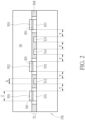
- FIG. 2 is a schematic, cross-sectional diagram taken along line I-I' in FIG. 1 after the assembly of the multi-row QFN package.
- the ball pad layout 1 fabricated in the top layer TL of a base substrate PB comprises staggered ball pads (or finger pads) including, for example, ball pads 101-103 arranged in the first row R1 and ball pads 201-205 arranged in the second row R2.
- the ball pads 101-103 and 201-205 may be copper pads, but is not limited thereto.
- the base substrate PB may comprise a printed circuit board or a package substrate, but is not limited thereto.
- the ball pads 101-103 and 201-205 are disposed within a surface mount region 10 for mounting a multi-row QFN package 50 ( FIG. 2 ) using surface mount techniques known in the art.
- the leads 501-503 on the bottom side of the multi-row QFN package 50 may be bonded to corresponding ball pads 101-103 and 201-205 with solder joints SN to form electrical connection paths.
- the ball pads 101-103 and 201-205 may be non-solder mask defined (NSMD) pads.
- the solder mask is omitted in FIG. 1 .
- the ball pads 101-103 arranged in the first row R1 are approximately aligned to one another along the first direction D1.
- the ball pads 201-205 arranged in the second row R2 are approximately aligned to one another along the first direction D1.
- the ball pads 101-103 and 201-205 may be arranged in a staggered manner in the second direction D2 that is orthogonal to the first direction D1.
- the ball pad 101 may be connected to a trace Tr1
- the ball pad 202 may be connected to a trace Tr2
- the ball pad 102 may be connected to a trace Tr3
- the ball pad 203 may be connected to a trace Tr4
- the ball pad 204 may be connected to a trace Tr5
- the ball pad 103 may be connected to a trace Tr6.
- the traces Tr1-Tr6 may extend along the second direction D2.
- the trace Tr2 passes through the routing space between the ball pad 101 and ball pad 102 in the first row R1.
- the two adjacent traces Tr4 and Tr5 pass through the routing space between the ball pad 102 and ball pad 103 in the first row R1.
- the traces Tr4 and Tr5 are designated as a differential pair, and the adjacent balls pads 102 and 103 are designated as ground pads, thereby constituting a ground-signal-signal-ground (GSSG) routing configuration.
- GSSG ground-signal-signal-ground
- the width of each of the ball pads 101-103 and 201-205 is labeled as Z
- the width of each of the traces Tr1-Tr6 is labeled as X
- the space between the passing traces Tr2, Tr4 and Tr5 and the ball pads 101-103 is labeled as Y
- FIG. 3 schematically shows the partial layout of the ball pads and the pad pitches according to an embodiment of the invention.
- the solder mask and the traces are omitted in FIG. 3 .
- the width Z of each of the ball pads 101-105 is 0.2mm.
- the first row R1 and the second row R2 are arranged with pitch P2.
- FIG. 3 also illustrates a basic pad unit PU consisting of five pads.
- the basic pad unit PU1 is composed of two ball pads 101 and 102 in the first row R1 and three ball pads 201-203 in the second row R2
- the next basic pad unit PU2 is composed of two ball pads 103 and 104 in the first row R1 and three ball pads 204-206 in the second row R2.
- the array of the ball pads for the multi-row QFN is constructed by repeating the basic pad units PU.
- the number of the ball pads can be increased by 4.5% for a 12.7mm x12.7mm dual-row QFN package (from 176 pins to 186 pins).
- the size of the dual-row QFN package can be reduced by 7.7% for a 176-pin dual-row QFN package (from 12.7mm x12.7mm to 12.2mm x12.2mm). Further, it is easier to assign the differential pair when routing the layout for the multi-row QFN packages.
- FIG. 4A to FIG. 4D illustrate a corner pad unit composed of a single, reversed-L-shaped pad and three square-shaped pads according to an embodiment of the invention.
- the reversed-L-shaped pad 401 is disposed at the location that is closest to the apex A of a corner of the surface mount region 10.
- the two edges of the reversed-L-shaped pad 401 may be perpendicular to the two adjacent sides of the surface mount region 10, respectively, as that shown in FIG. 4A and FIG. 4B .
- the two edges of the reversed-L-shaped pad 401 may be parallel with the two adjacent sides of the surface mount region 10, respectively, as that shown in FIG. 4C and FIG. 4D .
- the three square-shaped pads 402-404 are disposed around the reversed-L-shaped pad 401, thereby forming a 2x2 corner ball pad array, which can significantly improve the ball cracking problems.
- the spacing between the pads 401-404 may be equal to or greater than 0.18 mm, but is not limited thereto.
- the pads 401-404 may be dummy pads.
- the pads 401-404 may be ground pads and may be electrically connected to a ground plane of the PCB substrate.
- solder paste 401s, solder paste 402s, solder paste 403s, and solder paste 404s may be applied onto the respective pads 401-404 by using a screen printing method.
- the solder paste 402s, solder paste 403s, and solder paste 404s present a rounded corner corresponding to each corner of the square-shaped pads 402-404.
- FIG. 4B and FIG. 4D compared to the embodiments in FIG. 4A and FIG.
- solder paste 402s, solder paste 403s, and solder paste 404s occupy less surface area of each of the pads 402-404, and each of the solder paste 402s, solder paste 403s, and solder paste 404s presents a circular shape approximately about the center of each of the pads 402-404.
- the reversed-L-shaped pad 401 is completely covered with the solder paste 401s.
- FIG. 5A to FIG. 5D illustrate a corner pad unit composed of a single, reversed-L-shaped pad, two signal pads, and one square-shaped pad according to another embodiment of the invention.
- the reversed-L-shaped pad 501 is disposed at the location that is closest to the apex A of a corner of the surface mount region 10.
- the two edges of the reversed-L-shaped pad 501 may be perpendicular to the two sides of the surface mount region 10, respectively, as that shown in FIG. 5A and FIG. 5B .
- the two edges of the reversed-L-shaped pad 501 may be parallel with the two sides of the surface mount region 10, respectively, as that shown in FIG. 5C and FIG.
- the square-shaped pad 503 is disposed diagonally around the reversed-L-shaped pad 501 and the two signal pads 502 and 504 are arranged diagonally, thereby forming a 2x2 corner ball pad array, which can significantly improve the ball cracking problems.
- the spacing between the pads 501-504 may be equal to or greater than 0.18 mm, but is not limited thereto.
- the pads 501 and 503 may be dummy pads.
- the pads 501 and 503 may be ground pads and may be electrically connected to a ground plane of the PCB substrate.
- solder paste 501s, solder paste 502s, solder paste 503s, and solder paste 504s may be applied onto the respective pads 501-504 by using a screen printing method.
- the solder paste 503s when viewed from the above, presents a rounded corner corresponding to each corner of the pad 503.
- the solder paste 503s occupies less surface area of the pad 503, and the solder paste 503s presents a circular shape about the center of the pad 503.
- the reversed-L-shaped pad 501 and the two signal pads 502 and 504 are completely covered with the solder paste 501s, 502s, and 504s, respectively.
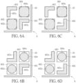
- FIG. 6A to FIG. 6D illustrate a corner pad unit composed of two reversed-L-shaped pads and two square-shaped pads according to still another embodiment of the invention.
- the reversed-L-shaped pad 601 is disposed at the location that is closest to the apex A of a corner of the surface mount region 10.
- the two edges of the reversed-L-shaped pad 601 may be perpendicular to the two sides of the surface mount region 10, respectively, as that shown in FIG. 6A and FIG. 6B .
- the two edges of the reversed-L-shaped pad 601 may be parallel with the two sides of the surface mount region 10, respectively, as that shown in FIG. 6C and FIG. 6D .
- the reversed-L-shaped pad 603 is disposed diagonally around the reversed-L-shaped pad 601 and the two square-shaped pads 602 and 604 are arranged diagonally, thereby forming a 2x2 corner ball pad array, which can significantly improve the ball cracking problems.
- the spacing between the pads 601-604 may be equal to or greater than 0.18 mm, but is not limited thereto.
- the pads 601-604 may be dummy pads.
- the pads 601-604 may be ground pads and may be electrically connected to a ground plane of the PCB substrate.
- solder paste 601s, solder paste 602s, solder paste 603s, and solder paste 604s may be applied onto the respective pads 601-604 by using a screen printing method.
- each of the solder paste 602s and solder paste 604s presents a rounded corner corresponding to each corner of the pads 602 and 604.
- FIG. 6B and FIG. 6D compared to the embodiments in FIG. 6A and FIG. 6C , each of the solder paste 602s and solder paste 604s occupies less surface area of each of the pads 602 and 604.
- Each of the solder paste 602s and solder paste 604s presents a circular shape about the center of each of the pads 602 and 604.
- the reversed-L-shaped pads 601 and 603 are completely covered with the solder paste 601s and 603s, respectively.
- FIG. 7A to FIG. 7D illustrate a corner pad unit composed of two reversed-L-shaped pads and two signal pads according to yet another embodiment of the invention.
- the reversed-L-shaped pad 701 is disposed at the location that is closest to the apex A of a corner of the surface mount region 10.
- the two edges of the reversed-L-shaped pad 701 may be perpendicular to the two sides of the surface mount region 10, respectively, as that shown in FIG. 7A and FIG. 7B .
- the two edges of the reversed-L-shaped pad 701 may be parallel with the two sides of the surface mount region 10, respectively, as that shown in FIG. 7C and FIG. 7D .
- the reversed-L-shaped pad 703 is disposed diagonally around the reversed-L-shaped pad 701 and the two signal pads 702 and 704 are arranged diagonally, thereby forming a 2x2 corner ball pad array, which can significantly improve the ball cracking problems.
- the spacing between the pads 701-704 may be equal to or greater than 0.18 mm, but is not limited thereto.
- the pads 701 and 703 may be dummy pads.
- the pads 701 and 703 may be ground pads and may be electrically connected to a ground plane of the PCB substrate.
- solder paste 701s, solder paste 702s, solder paste 703s, and solder paste 704s may be applied onto the respective pads 701-704 by using a screen printing method.
- the pads 701-704 are completely covered with the solder pastes 701s-704s, respectively.
Landscapes
- Electric Connection Of Electric Components To Printed Circuits (AREA)
- Physics & Mathematics (AREA)
- Geometry (AREA)
- Wire Bonding (AREA)
- Combinations Of Printed Boards (AREA)
Abstract
Description
- This application claims the benefit of
U.S. Provisional Application No. 63/296,011, filed on January 3rd, 2022 - The present disclosure relates to ball pad (or finger pad) layout of a base substrate. More particularly, the present disclosure relates to a board-level ball pad pattern for multi-row Quad Flat No lead (QFN) packages.
- The continuous advancement in technology and miniaturization of electronic components, hand held and communication devices require superior thermal-electrical performance and miniature packages. An advanced and complicated Integrated Circuit (IC) device often demands increase in number of I/O's while maintaining its small size, footprint and weight. A dual-row QFN is an ideal solution for such demanding applications.
- The multi-row QFN package is a plastic-encapsulated package with a copper leadframe substrate. The exposed die attach paddle on the bottom efficiently conducts heat to the PCB and provides a stable ground through down bonds or by electrical connections through conductive die attach material. The design of multi-row QFN packages allows for flexibility and enhances electrical performance to very high-speed operating frequencies.
- As known in the art, differential signaling has been employed on PCB routing for the multi-row QFN packages, which uses two complementary signals to transmit the one data signal, but the second signal is inverted from the first. The signal receiver uses the difference between the inverted and non-inverted signals to decipher the information. Using differential pair routing to transmit signals has benefits such as reduction in noise and EMI. However, the drawback is that it takes up more space.
- Further, to get the best performance out of the differential pair routing, the lines must be equal in length and the pairs must be routed together and at the same widths, which can be a problem when routing around obstacles on the circuit board such as vias or smaller components.
- It is known that temperature variation induces strengths between the different substrates due to their different coefficient of thermal expansion (CTE). As a result of both material property and geometric factors these strengths generate creep strain energy and fatigues on the different layers in the structure and on the soldering joints. Simulations performed with different QFN package options and with a number of thermal cycling conditions predict that the critical region is at the interface between pads located in the package corners and soldering material below pads.
- One object of the present invention is to provide an improved board-level ball pad pattern for multi-row QFN packages in order to solve the above-mentioned prior art problems or shortcomings. A board-level pad pattern according to the invention is defined in
independent claim 1. The dependent claims define preferred embodiments thereof. A semiconductor device according to the invention is defined in claim 15. - One aspect of the invention provides a board-level pad pattern including a corner pad unit disposed at a corner of a surface mount region for mounting a multi-row QFN package. The corner pad unit comprises at least a reversed-L-shaped pad. The reversed-L-shaped pad is disposed in proximity to an apex of the corner of the surface mount region.
- Preferably, two edges of the reversed-L-shaped pad are perpendicular to two adjacent sides of the surface mount region, respectively.
- Preferably, two edges of the reversed-L-shaped pad are parallel with two adjacent sides of the surface mount region, respectively.
- Preferably, the board-level pad pattern further includes three square-shaped pads disposed around the reversed-L-shaped pad, thereby forming a 2x2 corner ball pad array.
- Preferably, spacing between the reversed-L-shaped pad and the three square-shaped pads is equal to or greater than 0.18 mm.
- Preferably, the reversed-L-shaped pad and the three square-shaped pads are ground pads.
- Preferably, the reversed-L-shaped pad and the three square-shaped pads are dummy pads.
- Preferably, a solder paste is disposed on each of the three square-shaped pads, wherein the solder paste presents a rounded corner.
- Preferably, the board-level pad pattern further includes a square-shaped pad diagonally disposed around the reversed-L-shaped pad and two signal pads, thereby forming a 2x2 corner ball pad array.
- Preferably, the reversed-L-shaped pad and the square-shaped pad are ground pads.
- Preferably, the reversed-L-shaped pad and the square-shaped pad are dummy pads.
- Preferably, a solder paste is disposed on the square-shaped pad, wherein the solder paste presents a rounded corner.
- Preferably, the board-level pad pattern further includes two square-shaped pads diagonally disposed around the reversed-L-shaped pad and another reversed-L-shaped pad, thereby forming a 2x2 corner ball pad array.
- Preferably, the reversed-L-shaped pads and the square-shaped pads are ground pads.
- Preferably, the reversed-L-shaped pads and the square-shaped pads are dummy pads.
- Preferably, a solder paste is disposed on the square-shaped pad, wherein the solder paste presents a rounded corner.
- Preferably, the board-level pad pattern further includes two signal pads diagonally disposed around the reversed-L-shaped pad and another reversed-L-shaped pad, thereby forming a 2x2 corner ball pad array.
- Preferably, the reversed-L-shaped pads are ground pads.
- Preferably, the reversed-L-shaped pads are dummy pads.
- Another aspect of the invention provides a semiconductor device including a base substrate comprising a surface mount region, wherein a corner pad unit is disposed at a corner of the surface mount region, wherein the corner pad unit comprises at least a reversed-L-shaped pad, wherein the reversed-L-shaped pad is disposed in proximity to an apex of the corner of the surface mount region; and a multi-row QFN package mounted on the surface mount region. In particular, the semiconductor device according to the another aspect of the invention includes the board-level pad pattern and all its preferred features/embodiments according to the one aspect of the invention, i.e. the corner part unit defined and described in connection with the semiconductor device according to the another aspect of the invention is the corner part unit defined and described in connection with the board-level pad pattern according to the one aspect of the invention.
- These and other objectives of the present invention will no doubt become obvious to those of ordinary skill in the art after reading the following detailed description of the preferred embodiment that is illustrated in the various figures and drawings.
- The accompanying drawings are included to provide a further understanding of the invention and are incorporated in and constitute a part of this specification. The drawings illustrate embodiments of the invention and, together with the description, serve to explain the principles of the invention. In the drawings:
-
FIG. 1 shows a germane portion of an exemplary base top layer of a layout of ball pads for a multi-row QFN package according to one embodiment of the invention; -
FIG. 2 is a schematic, cross-sectional diagram taken along line I-I' inFIG. 1 after the assembly of the multi-row QFN package; -
FIG. 3 schematically shows the partial ball pad layout for a multi-row QFN package and the pad pitches according to an embodiment of the invention; -
FIG. 4A to FIG. 4D illustrate a corner pad unit composed of a single, reversed-L-shaped pad and three square-shaped pads according to an embodiment of the invention; -
FIG. 5A to FIG. 5D illustrate a corner pad unit composed of a single, reversed-L-shaped pad, two signal pads, and one square-shaped pad according to another embodiment of the invention; -
FIG. 6A to FIG. 6D illustrate a corner pad unit composed of two reversed-L-shaped pads and two square-shaped pads according to still another embodiment of the invention; and -
FIG. 7A to FIG. 7D illustrate a corner pad unit composed of two reversed-L-shaped pads and two signal pads according to yet another embodiment of the invention. - In the following detailed description of embodiments of the invention, reference is made to the accompanying drawings, which form a part hereof, and in which is shown by way of illustration specific preferred embodiments in which the disclosure may be practiced.
- These embodiments are described in sufficient detail to enable those skilled in the art to practice them, and it is to be understood that other embodiments may be utilized and that mechanical, chemical, electrical, and procedural changes may be made without departing from the spirit and scope of the present disclosure. The following detailed description is, therefore, not to be taken in a limiting sense, and the scope of embodiments of the present invention is defined only by the appended claims.
- It will be understood that when an element or layer is referred to as being "on", "connected to" or "coupled to" another element or layer, it can be directly on, connected or coupled to the other element or layer or intervening elements or layers may be present. In contrast, when an element is referred to as being "directly on," "directly connected to" or "directly coupled to" another element or layer, there are no intervening elements or layers present. Like numbers refer to like elements throughout. As used herein, the term "and/or" includes any and all combinations of one or more of the associated listed items.
-
FIG. 1 is a schematic diagram showing a germane portion of an exemplary base top layer of a layout of ball pads for a multi-row QFN package according to one embodiment of the invention.FIG. 2 is a schematic, cross-sectional diagram taken along line I-I' inFIG. 1 after the assembly of the multi-row QFN package. As shown inFIG. 1 andFIG. 2 , theball pad layout 1 fabricated in the top layer TL of a base substrate PB comprises staggered ball pads (or finger pads) including, for example, ball pads 101-103 arranged in the first row R1 and ball pads 201-205 arranged in the second row R2. Preferably, for example, the ball pads 101-103 and 201-205 may be copper pads, but is not limited thereto. The base substrate PB may comprise a printed circuit board or a package substrate, but is not limited thereto. - Preferably, the ball pads 101-103 and 201-205 are disposed within a
surface mount region 10 for mounting a multi-row QFN package 50 (FIG. 2 ) using surface mount techniques known in the art. The leads 501-503 on the bottom side of themulti-row QFN package 50 may be bonded to corresponding ball pads 101-103 and 201-205 with solder joints SN to form electrical connection paths. Preferably, for example, the ball pads 101-103 and 201-205 may be non-solder mask defined (NSMD) pads. For the sake of simplicity, the solder mask is omitted inFIG. 1 . - Preferably, the ball pads 101-103 arranged in the first row R1 are approximately aligned to one another along the first direction D1. Preferably, the ball pads 201-205 arranged in the second row R2 are approximately aligned to one another along the first direction D1. Preferably, the ball pads 101-103 and 201-205 may be arranged in a staggered manner in the second direction D2 that is orthogonal to the first direction D1.
- Preferably, for example, the
ball pad 101 may be connected to a trace Tr1, theball pad 202 may be connected to a trace Tr2, theball pad 102 may be connected to a trace Tr3, theball pad 203 may be connected to a trace Tr4, theball pad 204 may be connected to a trace Tr5, and theball pad 103 may be connected to a trace Tr6. Preferably, for example, the traces Tr1-Tr6 may extend along the second direction D2. - Preferably, for example, only the trace Tr2 passes through the routing space between the
ball pad 101 andball pad 102 in the first row R1. Preferably, for example, the two adjacent traces Tr4 and Tr5 pass through the routing space between theball pad 102 andball pad 103 in the first row R1. Preferably, for example, the traces Tr4 and Tr5 are designated as a differential pair, and theadjacent balls pads FIG. 1 , the width of each of the ball pads 101-103 and 201-205 is labeled as Z, the width of each of the traces Tr1-Tr6 is labeled as X, and the space between the passing traces Tr2, Tr4 and Tr5 and the ball pads 101-103 is labeled as Y -
FIG. 3 schematically shows the partial layout of the ball pads and the pad pitches according to an embodiment of the invention. For the sake of simplicity, the solder mask and the traces are omitted inFIG. 3 . As shown inFIG. 3 , preferably, the ball pads 101-105 in the first row R1 are arranged at two different pitches P1 and P2, for example, P1=0.5mm and P2=0.7mm. Preferably, P1=X+2Y+Z and P2=2X+3Y+Z. Preferably, for example, the ball pads 201-205 in the second row R2 are arranged at a constant pitch P3 of about 0.4 mm, which is equal to the width Z of each of the ball pads 101-105 plus the interval of two adjacent ball pads of about 0.18-0.2mm (P3 =Z+V, where V=0.18-0.2 mm). Preferably, for example, the width Z of each of the ball pads 101-105 is 0.2mm. The first row R1 and the second row R2 are arranged with pitch P2. -
FIG. 3 also illustrates a basic pad unit PU consisting of five pads. For example, the basic pad unit PU1 is composed of twoball pads ball pads - It is advantageous to use the present invention because the number of the ball pads can be increased by 4.5% for a 12.7mm x12.7mm dual-row QFN package (from 176 pins to 186 pins). Alternatively, the size of the dual-row QFN package can be reduced by 7.7% for a 176-pin dual-row QFN package (from 12.7mm x12.7mm to 12.2mm x12.2mm). Further, it is easier to assign the differential pair when routing the layout for the multi-row QFN packages.
-
FIG. 4A to FIG. 4D illustrate a corner pad unit composed of a single, reversed-L-shaped pad and three square-shaped pads according to an embodiment of the invention. As shown inFIG. 4A to FIG. 4D , the reversed-L-shapedpad 401 is disposed at the location that is closest to the apex A of a corner of thesurface mount region 10. The two edges of the reversed-L-shapedpad 401 may be perpendicular to the two adjacent sides of thesurface mount region 10, respectively, as that shown inFIG. 4A and FIG. 4B . Alternatively, the two edges of the reversed-L-shapedpad 401 may be parallel with the two adjacent sides of thesurface mount region 10, respectively, as that shown inFIG. 4C and FIG. 4D . The three square-shaped pads 402-404 are disposed around the reversed-L-shapedpad 401, thereby forming a 2x2 corner ball pad array, which can significantly improve the ball cracking problems. - Preferably, for example, the spacing between the pads 401-404 may be equal to or greater than 0.18 mm, but is not limited thereto. Preferably, the pads 401-404 may be dummy pads. Alternatively preferably, the pads 401-404 may be ground pads and may be electrically connected to a ground plane of the PCB substrate.
- Preferably,
solder paste 401s,solder paste 402s,solder paste 403s, andsolder paste 404s may be applied onto the respective pads 401-404 by using a screen printing method. InFIG. 4A and FIG. 4C , when viewed from the above, thesolder paste 402s,solder paste 403s, andsolder paste 404s present a rounded corner corresponding to each corner of the square-shaped pads 402-404. InFIG. 4B and FIG. 4D , compared to the embodiments inFIG. 4A and FIG. 4C , thesolder paste 402s,solder paste 403s, andsolder paste 404s occupy less surface area of each of the pads 402-404, and each of thesolder paste 402s,solder paste 403s, andsolder paste 404s presents a circular shape approximately about the center of each of the pads 402-404. InFIG. 4A to FIG. 4D , the reversed-L-shapedpad 401 is completely covered with thesolder paste 401s. By providing such rounded corners or circular shape of thesolder paste 402s,solder paste 403s, andsolder paste 404s, the SMT stability and solder joint reliability can be improved. -
FIG. 5A to FIG. 5D illustrate a corner pad unit composed of a single, reversed-L-shaped pad, two signal pads, and one square-shaped pad according to another embodiment of the invention. As shown inFIG. 5Ato FIG. 5D , likewise, the reversed-L-shapedpad 501 is disposed at the location that is closest to the apex A of a corner of thesurface mount region 10. The two edges of the reversed-L-shapedpad 501 may be perpendicular to the two sides of thesurface mount region 10, respectively, as that shown inFIG. 5A and FIG. 5B . Alternatively, the two edges of the reversed-L-shapedpad 501 may be parallel with the two sides of thesurface mount region 10, respectively, as that shown inFIG. 5C and FIG. 5D . The square-shapedpad 503 is disposed diagonally around the reversed-L-shapedpad 501 and the twosignal pads - Preferably, for example, the spacing between the pads 501-504 may be equal to or greater than 0.18 mm, but is not limited thereto. Preferably, the
pads pads - Preferably,
solder paste 501s,solder paste 502s,solder paste 503s, andsolder paste 504s may be applied onto the respective pads 501-504 by using a screen printing method. InFIG. 5A and FIG. 5C , when viewed from the above, thesolder paste 503s presents a rounded corner corresponding to each corner of thepad 503. InFIG. 5B and FIG. 5D , compared to the embodiments inFIG. 5A and FIG. 5C , thesolder paste 503s occupies less surface area of thepad 503, and thesolder paste 503s presents a circular shape about the center of thepad 503. InFIG. 5A to FIG. 5D , the reversed-L-shapedpad 501 and the twosignal pads solder paste -
FIG. 6A to FIG. 6D illustrate a corner pad unit composed of two reversed-L-shaped pads and two square-shaped pads according to still another embodiment of the invention. As shown inFIG. 6A to FIG. 6D , the reversed-L-shapedpad 601 is disposed at the location that is closest to the apex A of a corner of thesurface mount region 10. The two edges of the reversed-L-shapedpad 601 may be perpendicular to the two sides of thesurface mount region 10, respectively, as that shown inFIG. 6A and FIG. 6B . Alternatively, the two edges of the reversed-L-shapedpad 601 may be parallel with the two sides of thesurface mount region 10, respectively, as that shown inFIG. 6C and FIG. 6D . The reversed-L-shapedpad 603 is disposed diagonally around the reversed-L-shapedpad 601 and the two square-shapedpads - Preferably, for example, the spacing between the pads 601-604 may be equal to or greater than 0.18 mm, but is not limited thereto. Preferably, the pads 601-604 may be dummy pads. Alternatively preferably, the pads 601-604 may be ground pads and may be electrically connected to a ground plane of the PCB substrate.
- Preferably,
solder paste 601s,solder paste 602s,solder paste 603s, andsolder paste 604s may be applied onto the respective pads 601-604 by using a screen printing method. InFIG. 6A and FIG. 6C , when viewed from the above, each of thesolder paste 602s andsolder paste 604s presents a rounded corner corresponding to each corner of thepads FIG. 6B and FIG. 6D , compared to the embodiments inFIG. 6A and FIG. 6C , each of thesolder paste 602s andsolder paste 604s occupies less surface area of each of thepads solder paste 602s andsolder paste 604s presents a circular shape about the center of each of thepads FIG. 6A to FIG. 6D , the reversed-L-shapedpads solder paste -
FIG. 7A to FIG. 7D illustrate a corner pad unit composed of two reversed-L-shaped pads and two signal pads according to yet another embodiment of the invention. As shown inFIG. 7Ato FIG. 7D , the reversed-L-shapedpad 701 is disposed at the location that is closest to the apex A of a corner of thesurface mount region 10. The two edges of the reversed-L-shapedpad 701 may be perpendicular to the two sides of thesurface mount region 10, respectively, as that shown inFIG. 7A and FIG. 7B . Alternatively, the two edges of the reversed-L-shapedpad 701 may be parallel with the two sides of thesurface mount region 10, respectively, as that shown inFIG. 7C and FIG. 7D . The reversed-L-shapedpad 703 is disposed diagonally around the reversed-L-shapedpad 701 and the twosignal pads - Preferably, for example, the spacing between the pads 701-704 may be equal to or greater than 0.18 mm, but is not limited thereto. Preferably, the
pads pads - Preferably,
solder paste 701s,solder paste 702s,solder paste 703s, andsolder paste 704s may be applied onto the respective pads 701-704 by using a screen printing method. InFIG. 7Ato FIG. 7D , the pads 701-704 are completely covered with the solder pastes 701s-704s, respectively. - Those skilled in the art will readily observe that numerous modifications and alterations of the device and method may be made while retaining the teachings of the invention. Accordingly, the above disclosure should be construed as limited only by the metes and bounds of the appended claims.
Claims (15)
- A board-level pad pattern, comprising:
a corner pad unit disposed at a corner of a surface mount region (10) for mounting a multi-row QFN package (50), wherein the corner pad unit comprises at least a reversed-L-shaped pad (401; 501; 601; 701), wherein the reversed-L-shaped pad (401; 501; 601; 701) is disposed in proximity to an apex (A) of the corner of the surface mount region (10). - The board-level pad pattern according to claim 1, wherein two edges of the reversed-L-shaped pad (401; 501; 601; 701) are perpendicular to two adjacent sides of the surface mount region (10), respectively; or
wherein two edges of the reversed-L-shaped pad (401; 501; 601; 701) are parallel with two adjacent sides of the surface mount region (10), respectively. - The board-level pad pattern according to claim 1 or 2, further comprising:
three square-shaped pads (402-404) disposed around the reversed-L-shaped pad (401), thereby forming a 2x2 corner ball pad array. - The board-level pad pattern according to claim 3, wherein spacing between the reversed-L-shaped pad (401) and the three square-shaped pads (402-404) is equal to or greater than 0.18 mm.
- The board-level pad pattern according to claim 3 or 4, wherein the reversed-L-shaped pad (401) and the three square-shaped pads (402-404) are ground pads; or
wherein the reversed-L-shaped pad (401) and the three square-shaped pads (402-404) are dummy pads. - The board-level pad pattern according to any one of claims 3 to 5, wherein a solder paste (402s-404s) is disposed on each of the three square-shaped pads (402-404), wherein the solder paste (402s-404s) presents a rounded corner.
- The board-level pad pattern according to claim 1 or 2, further comprising:
a square-shaped pad (503) diagonally disposed around the reversed-L-shaped pad (501) and two signal pads (502, 504), thereby forming a 2x2 corner ball pad array. - The board-level pad pattern according to claim 7, wherein the reversed-L-shaped pad (501) and the square-shaped pad (503) are ground pads; or
wherein the reversed-L-shaped pad (501) and the square-shaped pad (503) are dummy pads. - The board-level pad pattern according to claim 7 or 8, wherein a solder paste (503s) is disposed on the square-shaped pad (503), wherein the solder paste (503s) presents a rounded corner.
- The board-level pad pattern according to claim 1 or 2, further comprising:
two square-shaped pads (602, 604) diagonally disposed around the reversed-L-shaped pad (601) and another reversed-L-shaped pad (603), thereby forming a 2x2 corner ball pad array. - The board-level pad pattern according to claim 10, wherein the reversed-L-shaped pads (601, 603) and the two square-shaped pads (602, 604) are ground pads; or
wherein the reversed-L-shaped pads (601, 603) and the two square-shaped pads (602, 604) are dummy pads. - The board-level pad pattern according to claim 10 or 11, wherein a solder paste (602s, 604s) is disposed on each of the two square-shaped pads (602, 604), wherein the solder paste (602s, 604s) presents a rounded corner.
- The board-level pad pattern according to claim 1 or 2, further comprising:
two signal pads (702, 704) diagonally disposed around the reversed-L-shaped pad (701) and another reversed-L-shaped pad (703), thereby forming a 2x2 corner ball pad array. - The board-level pad pattern according to claim 13, wherein the reversed-L-shaped pads (701, 703) are ground pads; or
wherein the reversed-L-shaped pads (701, 703) are dummy pads. - A semiconductor device, comprising:a base substrate (PB) comprising a surface mount region (10), wherein a corner pad unit is disposed at a corner of the surface mount region (10), wherein the corner pad unit comprises at least a reversed-L-shaped pad (401; 501; 601; 701), wherein the reversed-L-shaped pad (401; 501; 601; 701) is disposed in proximity to an apex (A) of the corner of the surface mount region (10); anda multi-row QFN package (50) mounted on the surface mount region (10).
Applications Claiming Priority (2)
| Application Number | Priority Date | Filing Date | Title |
|---|---|---|---|
| US202263296011P | 2022-01-03 | 2022-01-03 | |
| US18/078,056 US12532758B2 (en) | 2022-01-03 | 2022-12-08 | Board-level pad pattern for multi-row QFN packages |
Publications (1)
| Publication Number | Publication Date |
|---|---|
| EP4207274A1 true EP4207274A1 (en) | 2023-07-05 |
Family
ID=84519741
Family Applications (1)
| Application Number | Title | Priority Date | Filing Date |
|---|---|---|---|
| EP22213332.4A Pending EP4207274A1 (en) | 2022-01-03 | 2022-12-14 | Board-level pad pattern for multi-row qfn packages |
Country Status (4)
| Country | Link |
|---|---|
| US (1) | US12532758B2 (en) |
| EP (1) | EP4207274A1 (en) |
| CN (1) | CN116387272A (en) |
| TW (1) | TWI841163B (en) |
Citations (9)
| Publication number | Priority date | Publication date | Assignee | Title |
|---|---|---|---|---|
| US6191491B1 (en) * | 1997-10-20 | 2001-02-20 | Rohm Co., Ltd. | Semiconductor integrated circuit device |
| JP2004077386A (en) * | 2002-08-21 | 2004-03-11 | Seiko Epson Corp | Inspection method of semiconductor mounting structure, mounting structure of semiconductor device, electro-optical device, and electronic apparatus |
| US20100001392A1 (en) * | 2008-07-04 | 2010-01-07 | Samsung Electronics Co., Ltd. | Semiconductor package |
| JP2011114071A (en) * | 2009-11-25 | 2011-06-09 | Renesas Electronics Corp | Semiconductor integrated circuit device, and method of arranging bonding pad for input/output of the same |
| US20120007195A1 (en) * | 2010-07-12 | 2012-01-12 | Analog Devices, Inc. | Apparatus for integrated circuit packaging |
| US20160119564A1 (en) * | 2014-10-23 | 2016-04-28 | Canon Kabushiki Kaisha | Electronic component, module and camera |
| WO2020196752A1 (en) * | 2019-03-28 | 2020-10-01 | 株式会社村田製作所 | Module |
| US20200402893A1 (en) * | 2019-06-24 | 2020-12-24 | Mediatek Inc. | Multi-row qfn semiconductor package |
| WO2021179504A1 (en) * | 2020-03-13 | 2021-09-16 | 华为技术有限公司 | Circuit board structure and electronic device |
Family Cites Families (51)
| Publication number | Priority date | Publication date | Assignee | Title |
|---|---|---|---|---|
| US5155065A (en) | 1992-03-16 | 1992-10-13 | Motorola, Inc. | Universal pad pitch layout |
| US5468999A (en) | 1994-05-26 | 1995-11-21 | Motorola, Inc. | Liquid encapsulated ball grid array semiconductor device with fine pitch wire bonding |
| JP2781787B2 (en) | 1996-08-29 | 1998-07-30 | 日本電気アイシーマイコンシステム株式会社 | Bonding pad arrangement of semiconductor chip and optimization method thereof |
| US5962926A (en) | 1997-09-30 | 1999-10-05 | Motorola, Inc. | Semiconductor device having multiple overlapping rows of bond pads with conductive interconnects and method of pad placement |
| JP3466064B2 (en) | 1997-10-20 | 2003-11-10 | ローム株式会社 | Semiconductor integrated circuit device |
| JP3429718B2 (en) | 1999-10-28 | 2003-07-22 | 新光電気工業株式会社 | Surface mounting substrate and surface mounting structure |
| US6603199B1 (en) | 2000-11-28 | 2003-08-05 | National Semiconductor Corporation | Integrated circuit package having die with staggered bond pads and die pad assignment methodology for assembly of staggered die in single-tier ebga packages |
| JP2002170844A (en) | 2000-12-04 | 2002-06-14 | Oki Electric Ind Co Ltd | Semiconductor device |
| US6552436B2 (en) | 2000-12-08 | 2003-04-22 | Motorola, Inc. | Semiconductor device having a ball grid array and method therefor |
| TW511193B (en) | 2001-12-13 | 2002-11-21 | Acer Labs Inc | Inner circuit structure of array type bonding pad chip and its manufacturing method |
| WO2003065451A1 (en) | 2002-01-31 | 2003-08-07 | Thomson Licensing S.A. | Flip chip die bond pads, die bond pad placement and routing optimization |
| US7709747B2 (en) | 2004-11-29 | 2010-05-04 | Fci | Matched-impedance surface-mount technology footprints |
| JP2007081374A (en) | 2005-09-12 | 2007-03-29 | Samsung Electronics Co Ltd | Semiconductor package, printed circuit board and semiconductor module having solder mask limited bonding pads and solder mask non-limiting bonding pads |
| US20070187808A1 (en) | 2006-02-16 | 2007-08-16 | Easic Corporation | Customizable power and ground pins |
| JP2007294768A (en) | 2006-04-26 | 2007-11-08 | Toshiba Corp | Semiconductor device |
| JP5120868B2 (en) | 2006-07-13 | 2013-01-16 | ルネサスエレクトロニクス株式会社 | Semiconductor device |
| US7477108B2 (en) | 2006-07-14 | 2009-01-13 | Micro Mobio, Inc. | Thermally distributed integrated power amplifier module |
| KR100773097B1 (en) | 2006-08-22 | 2007-11-02 | 삼성전자주식회사 | Semiconductor device with pad |
| US20080093749A1 (en) | 2006-10-20 | 2008-04-24 | Texas Instruments Incorporated | Partial Solder Mask Defined Pad Design |
| JP2009164195A (en) | 2007-12-28 | 2009-07-23 | Panasonic Corp | Semiconductor chip |
| DE112009000008T5 (en) | 2008-03-14 | 2010-09-30 | Murata Mfg. Co., Ltd., Nagaokakyo-shi | A method of smoothing an electrode, a method of manufacturing a ceramic substrate, and a ceramic substrate |
| JP2009302099A (en) | 2008-06-10 | 2009-12-24 | Nec Electronics Corp | Semiconductor device |
| JP5213034B2 (en) * | 2008-07-09 | 2013-06-19 | Necインフロンティア株式会社 | BGA package |
| GB0817834D0 (en) | 2008-09-30 | 2008-11-05 | Cambridge Silicon Radio Ltd | Low cost flexible substrate |
| JP2010278318A (en) | 2009-05-29 | 2010-12-09 | Renesas Electronics Corp | Semiconductor device |
| US8471154B1 (en) | 2009-08-06 | 2013-06-25 | Amkor Technology, Inc. | Stackable variable height via package and method |
| JP5467959B2 (en) | 2010-07-21 | 2014-04-09 | ルネサスエレクトロニクス株式会社 | Semiconductor device |
| JP5848517B2 (en) | 2011-04-26 | 2016-01-27 | ルネサスエレクトロニクス株式会社 | Semiconductor device |
| US8723337B2 (en) | 2011-07-14 | 2014-05-13 | Texas Instruments Incorporated | Structure for high-speed signal integrity in semiconductor package with single-metal-layer substrate |
| JP5968713B2 (en) | 2012-07-30 | 2016-08-10 | ルネサスエレクトロニクス株式会社 | Semiconductor device |
| US9257412B2 (en) * | 2012-09-12 | 2016-02-09 | Taiwan Semiconductor Manufacturing Company, Ltd. | Stress reduction apparatus |
| KR101512816B1 (en) | 2012-10-08 | 2015-04-17 | 한국전자통신연구원 | Flexible printed circuit board and optical communication module comprising the same |
| US9673093B2 (en) | 2013-08-06 | 2017-06-06 | STATS ChipPAC Pte. Ltd. | Semiconductor device and method of making wafer level chip scale package |
| US8975746B1 (en) | 2013-08-29 | 2015-03-10 | Broadcom Corporation | Ball arrangement for integrated circuit package devices |
| US9281293B2 (en) | 2013-10-30 | 2016-03-08 | Freescale Semiconductor Inc. | Microelectronic packages having layered interconnect structures and methods for the manufacture thereof |
| US9831205B2 (en) | 2013-11-18 | 2017-11-28 | Taiwan Semiconductor Manufacturing Company Ltd. | Semiconductor device and manufacturing method thereof |
| US9437566B2 (en) | 2014-05-12 | 2016-09-06 | Invensas Corporation | Conductive connections, structures with such connections, and methods of manufacture |
| CN104241753B (en) | 2014-09-03 | 2017-01-25 | 华南理工大学 | LTCC filtering balun adopting two inverse filtering circuits |
| EP3030059B1 (en) * | 2014-11-12 | 2018-08-15 | OSRAM GmbH | An electronic component and corresponding mounting method |
| US10231325B1 (en) | 2016-12-20 | 2019-03-12 | Juniper Networks, Inc. | Placement of vias in printed circuit board circuits |
| DE102017215027A1 (en) | 2017-08-28 | 2019-02-28 | Robert Bosch Gmbh | Semiconductor device and Kontaktieranordnung with a semiconductor device and a printed circuit board |
| JP7001530B2 (en) | 2018-04-16 | 2022-01-19 | ルネサスエレクトロニクス株式会社 | Semiconductor device |
| GB2591887B (en) | 2018-09-12 | 2022-05-25 | Mitsubishi Electric Corp | Microwave device and antenna |
| KR102600022B1 (en) | 2019-03-06 | 2023-11-07 | 삼성전기주식회사 | Manufacturing method of electronic device module |
| JP7273654B2 (en) | 2019-08-09 | 2023-05-15 | ルネサスエレクトロニクス株式会社 | Semiconductor device, manufacturing method thereof, and electronic device |
| TWI808292B (en) | 2019-12-30 | 2023-07-11 | 聯華電子股份有限公司 | Package structure of semiconductor device |
| CN111439034B (en) | 2020-05-13 | 2025-04-25 | 苏州锐发打印技术有限公司 | Piezoelectric inkjet printing device with through-holes on piezoelectric plate |
| US11502054B2 (en) | 2020-11-11 | 2022-11-15 | Nxp Usa, Inc. | Semiconductor device assembly and method therefor |
| US11804428B2 (en) | 2020-11-13 | 2023-10-31 | Qualcomm Incorporated | Mixed pad size and pad design |
| TWI741898B (en) * | 2020-12-03 | 2021-10-01 | 東龍投資股份有限公司 | Alignment pattern unit and semiconductor manufacturing process inspection system |
| CN113917747B (en) | 2021-09-30 | 2022-11-01 | 武汉华星光电技术有限公司 | Display panel and display device |
-
2022
- 2022-12-08 US US18/078,056 patent/US12532758B2/en active Active
- 2022-12-14 EP EP22213332.4A patent/EP4207274A1/en active Pending
- 2022-12-29 CN CN202211717713.0A patent/CN116387272A/en active Pending
- 2022-12-30 TW TW111150843A patent/TWI841163B/en active
Patent Citations (10)
| Publication number | Priority date | Publication date | Assignee | Title |
|---|---|---|---|---|
| US6191491B1 (en) * | 1997-10-20 | 2001-02-20 | Rohm Co., Ltd. | Semiconductor integrated circuit device |
| JP2004077386A (en) * | 2002-08-21 | 2004-03-11 | Seiko Epson Corp | Inspection method of semiconductor mounting structure, mounting structure of semiconductor device, electro-optical device, and electronic apparatus |
| US20100001392A1 (en) * | 2008-07-04 | 2010-01-07 | Samsung Electronics Co., Ltd. | Semiconductor package |
| JP2011114071A (en) * | 2009-11-25 | 2011-06-09 | Renesas Electronics Corp | Semiconductor integrated circuit device, and method of arranging bonding pad for input/output of the same |
| US20120007195A1 (en) * | 2010-07-12 | 2012-01-12 | Analog Devices, Inc. | Apparatus for integrated circuit packaging |
| US20160119564A1 (en) * | 2014-10-23 | 2016-04-28 | Canon Kabushiki Kaisha | Electronic component, module and camera |
| WO2020196752A1 (en) * | 2019-03-28 | 2020-10-01 | 株式会社村田製作所 | Module |
| US20200402893A1 (en) * | 2019-06-24 | 2020-12-24 | Mediatek Inc. | Multi-row qfn semiconductor package |
| WO2021179504A1 (en) * | 2020-03-13 | 2021-09-16 | 华为技术有限公司 | Circuit board structure and electronic device |
| EP4096371A1 (en) * | 2020-03-13 | 2022-11-30 | Huawei Technologies Co., Ltd. | Circuit board structure and electronic device |
Also Published As
| Publication number | Publication date |
|---|---|
| US12532758B2 (en) | 2026-01-20 |
| TWI841163B (en) | 2024-05-01 |
| CN116387272A (en) | 2023-07-04 |
| TW202329343A (en) | 2023-07-16 |
| US20230215798A1 (en) | 2023-07-06 |
Similar Documents
| Publication | Publication Date | Title |
|---|---|---|
| US6509530B2 (en) | Via intersect pad for electronic components and methods of manufacture | |
| JPH09283695A (en) | Semiconductor mounting structure | |
| CN102301469A (en) | Integrated-circuit Attachment Structure With Solder Balls And Pins | |
| US20080078571A1 (en) | Device mounting board and semiconductor module | |
| US20070169342A1 (en) | Connection pad layouts | |
| US7230332B2 (en) | Chip package with embedded component | |
| JP2000232180A (en) | Wiring board and semiconductor device | |
| EP4207272A1 (en) | Board-level pad pattern for multi-row qfn packages | |
| US12532758B2 (en) | Board-level pad pattern for multi-row QFN packages | |
| EP4207273A1 (en) | Board-level pad pattern for multi-row qfn packages | |
| TW421860B (en) | Semiconductor device | |
| US20090284941A1 (en) | Semiconductor package, mounting circuit board, and mounting structure | |
| CN101601129B (en) | Mounting board and electronic device | |
| CN114765924B (en) | electronic device | |
| JP7531488B2 (en) | Semiconductor Device | |
| US20230411271A1 (en) | Integrated circuit packages | |
| US20250006685A1 (en) | Semiconductor packages with multiple types of conductive components | |
| US12635545B2 (en) | Ball map pattern | |
| US20240332154A1 (en) | Ball map pattern | |
| CN100378980C (en) | Semiconductor device | |
| US20060263934A1 (en) | Chip-type micro-connector and method of packaging the same | |
| CN118693029A (en) | Isolator | |
| CN119230508A (en) | Semiconductor package having multiple types of conductive elements |
Legal Events
| Date | Code | Title | Description |
|---|---|---|---|
| PUAI | Public reference made under article 153(3) epc to a published international application that has entered the european phase |
Free format text: ORIGINAL CODE: 0009012 |
|
| STAA | Information on the status of an ep patent application or granted ep patent |
Free format text: STATUS: THE APPLICATION HAS BEEN PUBLISHED |
|
| AK | Designated contracting states |
Kind code of ref document: A1 Designated state(s): AL AT BE BG CH CY CZ DE DK EE ES FI FR GB GR HR HU IE IS IT LI LT LU LV MC ME MK MT NL NO PL PT RO RS SE SI SK SM TR |
|
| STAA | Information on the status of an ep patent application or granted ep patent |
Free format text: STATUS: REQUEST FOR EXAMINATION WAS MADE |
|
| 17P | Request for examination filed |
Effective date: 20231228 |
|
| RBV | Designated contracting states (corrected) |
Designated state(s): AL AT BE BG CH CY CZ DE DK EE ES FI FR GB GR HR HU IE IS IT LI LT LU LV MC ME MK MT NL NO PL PT RO RS SE SI SK SM TR |