EP4203189A1 - Monopolare patch-drahtantenne mit erweiterter bandbreite - Google Patents
Monopolare patch-drahtantenne mit erweiterter bandbreite Download PDFInfo
- Publication number
- EP4203189A1 EP4203189A1 EP22215644.0A EP22215644A EP4203189A1 EP 4203189 A1 EP4203189 A1 EP 4203189A1 EP 22215644 A EP22215644 A EP 22215644A EP 4203189 A1 EP4203189 A1 EP 4203189A1
- Authority
- EP
- European Patent Office
- Prior art keywords
- wire
- antenna
- capacitive
- ground plane
- impedance matching
- Prior art date
- Legal status (The legal status is an assumption and is not a legal conclusion. Google has not performed a legal analysis and makes no representation as to the accuracy of the status listed.)
- Pending
Links
Images


Classifications
-
- H—ELECTRICITY
- H01—ELECTRIC ELEMENTS
- H01Q—ANTENNAS, i.e. RADIO AERIALS
- H01Q9/00—Electrically-short antennas having dimensions not more than twice the operating wavelength and consisting of conductive active radiating elements
- H01Q9/04—Resonant antennas
- H01Q9/0407—Substantially flat resonant element parallel to ground plane, e.g. patch antenna
- H01Q9/045—Substantially flat resonant element parallel to ground plane, e.g. patch antenna with particular feeding means
- H01Q9/0457—Substantially flat resonant element parallel to ground plane, e.g. patch antenna with particular feeding means electromagnetically coupled to the feed line
-
- H—ELECTRICITY
- H01—ELECTRIC ELEMENTS
- H01Q—ANTENNAS, i.e. RADIO AERIALS
- H01Q1/00—Details of, or arrangements associated with, antennas
- H01Q1/27—Adaptation for use in or on movable bodies
-
- H—ELECTRICITY
- H01—ELECTRIC ELEMENTS
- H01Q—ANTENNAS, i.e. RADIO AERIALS
- H01Q1/00—Details of, or arrangements associated with, antennas
- H01Q1/48—Earthing means; Earth screens; Counterpoises
-
- H—ELECTRICITY
- H01—ELECTRIC ELEMENTS
- H01Q—ANTENNAS, i.e. RADIO AERIALS
- H01Q5/00—Arrangements for simultaneous operation of antennas on two or more different wavebands, e.g. dual-band or multi-band arrangements
- H01Q5/30—Arrangements for providing operation on different wavebands
- H01Q5/307—Individual or coupled radiating elements, each element being fed in an unspecified way
- H01Q5/342—Individual or coupled radiating elements, each element being fed in an unspecified way for different propagation modes
- H01Q5/357—Individual or coupled radiating elements, each element being fed in an unspecified way for different propagation modes using a single feed point
-
- H—ELECTRICITY
- H01—ELECTRIC ELEMENTS
- H01Q—ANTENNAS, i.e. RADIO AERIALS
- H01Q5/00—Arrangements for simultaneous operation of antennas on two or more different wavebands, e.g. dual-band or multi-band arrangements
- H01Q5/50—Feeding or matching arrangements for broad-band or multi-band operation
-
- H—ELECTRICITY
- H01—ELECTRIC ELEMENTS
- H01Q—ANTENNAS, i.e. RADIO AERIALS
- H01Q9/00—Electrically-short antennas having dimensions not more than twice the operating wavelength and consisting of conductive active radiating elements
- H01Q9/04—Resonant antennas
- H01Q9/0407—Substantially flat resonant element parallel to ground plane, e.g. patch antenna
- H01Q9/0421—Substantially flat resonant element parallel to ground plane, e.g. patch antenna with a shorting wall or a shorting pin at one end of the element
-
- H—ELECTRICITY
- H01—ELECTRIC ELEMENTS
- H01Q—ANTENNAS, i.e. RADIO AERIALS
- H01Q9/00—Electrically-short antennas having dimensions not more than twice the operating wavelength and consisting of conductive active radiating elements
- H01Q9/04—Resonant antennas
- H01Q9/0407—Substantially flat resonant element parallel to ground plane, e.g. patch antenna
- H01Q9/045—Substantially flat resonant element parallel to ground plane, e.g. patch antenna with particular feeding means
-
- H—ELECTRICITY
- H01—ELECTRIC ELEMENTS
- H01Q—ANTENNAS, i.e. RADIO AERIALS
- H01Q9/00—Electrically-short antennas having dimensions not more than twice the operating wavelength and consisting of conductive active radiating elements
- H01Q9/04—Resonant antennas
- H01Q9/30—Resonant antennas with feed to end of elongated active element, e.g. unipole
- H01Q9/32—Vertical arrangement of element
- H01Q9/36—Vertical arrangement of element with top loading
Definitions
- the present invention relates to the field of antennas and more particularly to miniature antennas which can be integrated into on-board systems. More specifically, the invention relates to antennas of the monopolar wire-plate type.
- the invention finds application, by way of nonlimiting examples, in radiocommunication systems or in systems for the geolocation of moving objects.
- miniature antenna means an antenna having dimensions of the order of the wavelength of the minimum operating resonant frequency, divided by 2 ⁇ .
- Miniature antennas have the advantage of being compatible with embedded systems and integrated circuits widely used in the fields of mobile devices, telephony, geolocation.
- the miniaturization of an antenna reduces the performance of the antenna in terms of bandwidth. The more the dimensions of the antenna are reduced with respect to the operating wavelength to improve its integrability, the less the bandwidth BW is wide.
- the quality coefficient of the antenna Q is introduced inversely proportional to the bandwidth BW of the miniaturized antenna.
- Bandwidth means the range of frequencies in which the transfer of energy from the power supply to the antenna or from the antenna to the receiver is maximized.
- the bandwidth can be defined according to a criterion according to the reflection coefficient of the antenna. In what follows, we choose a criterion of "less than -6dB" as the limit of the reflection coefficient as a function of the frequency to determine the passband. This criterion is given as an example only.
- quality factor Q is meant the parameter indicating the damping rate of the antenna equal to the ratio of the resonant frequency to the bandwidth.
- An antenna with a high quality factor radiates very efficiently at the radiation frequency over a very narrow frequency band.
- Q f 0 BW .
- antennas of the monopolar "Wire Plate” type present a possible compact solution for an antenna with omnidirectional radiation suitable for many wireless communication applications.
- This type of antenna belongs to both the family of printed antennas and charged monopole antennas.
- these antennas are still the subject of numerous improvement and development works to improve their compactness and also to widen their operating band. This balance between miniaturization and performance is essential to be in phase with the evolution of the flow of data communicated between the different systems and the densification of the implementation of the hardware architectures of these systems.
- a miniaturized wire-plate antenna In general, a miniaturized wire-plate antenna according to the state of the art combines two resonance modes: a first resonance in the low-frequency domain with a frequency f 1 between 0.7 Ghz and 1 Ghz (GSM band) and a resonance of the fundamental mode TM 01 at a frequency f 0 greater than 2 Ghz.
- a technical problem to be solved is the production of a miniaturized antenna making it possible to widen the bandwidth without enlarging the electrical dimensions of the antenna or degrading its quality factor.
- the invention finds its application in the context of radio communication devices with high integration density.
- the European patent EP3235058B1 describes a wire-plate antenna having an etched slot at the capacitive roof to widen the bandwidth of the antenna.
- a disadvantage of the solution proposed by this patent is that the proposed antenna loses its omnidirectional radiation and changes the polarization of the electromagnetic field towards the high operating frequencies.
- the invention proposes several embodiments of a wire-plate type antenna having a new structure for adapting the input impedance of the antenna so as to widen the bandwidth.
- the solution according to the invention consists of modifying the input impedance of the antenna by means of the simultaneous insertion of a parasitic capacitive element and a parasitic inductive element. This geometric modification makes it possible to modify the spectral response of the antenna by exciting an additional resonance mode. The excitation of two close resonance modes allows the bandwidth to be increased in the target frequency range. Moreover, this solution does not disturb the conventional upper modes of the printed antenna, in particular the fundamental TM 01 directional mode.
- This approach can be applied using different forms of parasitic element, and it is particularly relevant for the family of monopolar plate wire antennas dedicated to the various mobile wireless communication systems in particular the GSM band in uplink (UpLink) and downlink ( DownLink).
- the structure proposed according to the invention differs from known solutions in particular by the possibility of widening the bandwidth in the low frequency domain without degradation of the fundamental mode.
- an advantage of the antenna according to the invention is that the technique is simple to implement.
- the modified structure can be made with common manufacturing techniques without the need for costly changes to the production line. This results in an antenna with reduced bulk and increased bandwidth. All of these advantages thus make the structure according to the invention a promising solution for applications of compact, broadband and multi-band miniaturized antennas.
- the separation distance between the ground plane and the capacitive roof is between one fiftieth of the first resonant wavelength and one tenth of the first resonant wavelength.
- the separation distance between the ground plane and the capacitive roof is between the fiftieth of the first wavelength of resonance and the fifteenth of the first resonant wavelength, or even the twentieth of the first resonant wavelength.
- the capacitive roof is produced by a conductive layer forming a flat rectangular surface with a width and/or a length comprised between one tenth of the first resonance wavelength and one quarter of the first resonance wavelength.
- the width and/or the length of the impedance matching wire is chosen according to the value of the bandwidth defined by the first and the second resonance mode.
- the volume of dielectric material separating the capacitive roof and the supply probe is a volume of air.
- the impedance matching wire is a metal rod.
- the impedance matching wire is a metal track deposited on the underside of the substrate.
- the short-circuit wire is connected to the capacitive roof through a via passing through the substrate from its lower face towards its upper face.
- the substrate is confined between the end of the supply probe and the capacitive roof so as to produce the volume of dielectric material.
- the feed probe is inserted into the substrate through a non-through via starting from its lower face.
- the short-circuit wire and the supply probe are perpendicular to the ground plane and to the capacitive roof.
- the antenna also comprises a discrete component mounted in series or in parallel on the impedance matching wire to adjust the value of the impedance of the LC type parallel circuit.
- the invention also relates to a geolocation device intended to be embedded in a moving object comprising at least one antenna of the wire-plate type according to the invention configured to transmit to a remote server, via a communication system, the different positions of the moving object.
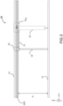
- FIG. 1 illustrates a view in section along the plane (x, z) of a wire-plate type antenna according to the state of the art intended to be embedded in a radiocommunication system.
- the wire-plate antenna 10' comprises a ground plane 11'; a capacitive roof 12'; a power supply probe 13' and at least one electrically conductive short-circuit wire 14', connecting the capacitive roof 12' and the ground plane 11'.
- Ground plane 11' is produced by a metal layer and electrically connected to the overall electrical ground of the system in which the antenna is embedded.
- the ground plane can have rectangular, square or circular shapes by way of example.
- the ground plane 11' can be deposited on the upper face of a lower substrate, not shown.
- the capacitive roof is produced by a metal layer placed parallel to the ground plane 11' at a predetermined separation distance.
- the capacitive roof can have rectangular, square or circular shapes by way of example.
- the supply probe 13' can be produced by extending the central core of a coaxial cable passing through the ground plane 11' as far as the capacitive roof 12'. Blade central part of the power supply probe is connected on the one hand to a voltage generator (not shown) and on the other hand to the capacitive roof 12'.
- the central core of the feed probe 13' is electrically isolated from the ground plane 11' connected to the outer shield of the coaxial cable.
- the combination of the feed probe 13' with the capacitive roof 12' placed opposite the ground plane 11' excites the fundamental resonance mode TM 01 of the antenna at a frequency f 0 .
- the short-circuit wire 14' forms a metallic ground return causing the excitation of a first resonance mode in the low-frequency range at a frequency f 1 lower than that of the fundamental mode f 0 .
- the frequency f 1 of the “low frequency wire-plate” mode is of the order of a half to a quarter of the frequency f 0 of the fundamental mode.
- the short-circuit wire 14' can be made with a metal rod of cylindrical or parallelepiped shape, by way of example.
- the physical parameters influencing the frequencies f 0 and f 1 are the permittivity of the dielectric material which occupies the confined volume between the capacitive roof 12' and the ground plane 11', the distance between the capacitive roof 12' and the ground plane 11', the radius of the supply probe 13', the radius of the short-circuit wire 14', the distance between supply probe 13' and short-circuit wire 14', as well as the surface dimensions of the roof capacitor 12' and the ground plane 11'.
- the new structure of the proposed wire-plate antenna aims to widen the bandwidth around the frequency f 1 of the first resonance mode in the low frequency domain without degrading the operation of the fundamental mode. at f 0 and without increasing the dimensions of the various elements of the antenna detailed above.
- antenna wire-plate 10 comprises a ground plane 11; a capacitive roof 12; a power supply probe 13 and at least one electrically conductive short-circuit wire 14, connecting the capacitive roof 12 and the ground plane 11 and at least one impedance matching wire 15, electrically conductive, electrically connecting the wire shorting conductor 14 and supply probe 13.
- the capacitive roof 12 rests mechanically on the rod constituting the short-circuit wire 14, and the dielectric material confined between the capacitive roof 12 and the ground plane 11 is air.
- electrically insulating material plastic for example
- the supply probe 13 can be produced by the central core of a coaxial cable passing through the ground plane 11 towards the capacitive roof 12 but without touching said roof.
- the central core of feed probe 13 is electrically isolated from ground plane 11 which is connected to the outer shield of the coaxial cable.
- the central core of the feed probe is connected on the one hand to a voltage generator (not shown) and on the other hand stops before the capacitive roof 13 at a second predetermined separation distance H′.
- the end of the supply probe 13 is separated from the capacitive roof 12 by a volume of dielectric material so as to create a parasitic capacitive element C by .
- the separating dielectric material is air.
- the parasitic capacitive element C par is then connected in series between the supply probe 13 and the capacitive roof 12.
- the value of the capacitance of the parasitic capacitive element C par depends on the permittivity of the material confined between the end of the probe and the roof, the radius of the probe and the second separation distance H'.
- an impedance matching wire 15 creates a parasitic inductive element L par between the supply probe 13 and the short-circuit wire 14.
- the value of the inductance of the parasitic inductive element L par depends on the length of the wire and on its diameter in the case of a cylindrical rod for example.
- the combination of the parasitic capacitive element C par and the parasitic inductance L par forms an LC type parallel circuit mounted between the end of the supply probe 13 and the capacitive roof 12.
- This LC type parallel circuit excites a second resonance mode in the low-frequency domain at a frequency f 2 close to the first frequency f 1 of the first resonance mode in the low-frequency domain.
- the absolute value of the difference between the first frequency f 1 and the second frequency f 2 is between 1.1 GHz and 1.5 GHz.
- the insertion of the impedance matching wire 15 and the spacer made of dielectric material between the supply probe and the capacitive roof made it possible to obtain an additional resonance at a second resonance wavelength ⁇ 2 lower than the first resonance wavelength ⁇ 1 (associated with f 1 ).
- the short-circuit wire 14' always forms an active metal return to ground causing the excitation of the first resonance mode in the low-frequency domain at a frequency f 1 .
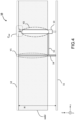
- FIG. 3 illustrates a sectional view along the (x,z) plane illustrating a wire-plate type antenna 10 according to a second embodiment of the invention.
- the second embodiment uses the same concept with the addition of the impedance matching wire 15 and the separation of the end of the probe 13 from the capacitive roof 12.
- the antenna 10 of the picture 3 further comprises a sustained substrate on which the capacitive roof 12 rests.
- the layer can be produced by common deposition techniques to obtain a copper layer, for example with a thickness of 18 ⁇ m.
- the substrate undergone may be a printed circuit support of the PCB type (acronym for Printed Circuit Board).
- the impedance matching wire 15 can be made by printing (or depositing) a metal track (or metal tape) on the underside of substrate sub1.
- the undergone substrate thus performs a mechanical function by acting as a support for the capacitive roof 12 and for the impedance matching wire 15.
- the undergone substrate also performs an electrical function. Indeed, being confined between the upper end of the supply probe 13 and the lower face of the capacitive roof, the volume of dielectric material of the parasitic capacitance C par is produced with the substrate undergone. Concerning the dielectric volume between the capacitive roof 12 and the ground plane 11, it remains mostly filled with air considering the low thickness of the substrate undergone with respect to the first separation distance H.
- the short-circuit wire 14 is connected to the capacitive roof 12 through a via V1 crossing the substrate undergone from its lower face towards its upper face on which the capacitive roof 12 rests.
- FIG 4 shows a sectional view along the (x,z) plane illustrating a wire-plate type antenna 10 according to a third embodiment of the invention.
- the third embodiment uses the same concept with the addition of the impedance matching wire 15 and the separation of the end of the probe 13 from the capacitive roof 12.
- the antenna 10 of the picture 3 further comprises a sustained substrate on which the capacitive roof 12 rests in the same manner as the second embodiment.
- the third embodiment differs from the second embodiment by a greater substrate thickness.
- the substrate sub2 is not confined between the upper end of the supply probe 12 but occupies a larger part of the volume delimited by the capacitive roof 12 and the ground plane 11.
- the substrate sub2 comprises a first through via V1 containing a part of the short-circuit wire 14 as far as the capacitive roof 12.
- the sub2 substrate further comprises a second non-through via V2 starting from its lower face without leading to the interface of the sub2 substrate with the capacitive roof 12.
- the part upper part of the supply probe 12 is then inserted into the non-through via V2.
- the volume of the substrate sub2 confined between the upper end of the supply probe 13 and the lower face of the capacitive roof 12 forms the dielectric of the capacitive element C by
- the dielectric material that forms the substrate sub2 must be chosen such that its electrical permittivity is limited, for example less than 6, preferably equal to 2, so as not to disturb the electromagnetic behavior of the antenna.
- the impedance matching wire 15 by printing (or depositing) a metal track (or metal strip) on the underside of the substrate sub2.
- Substrate undergone thus performs a mechanical function by playing the role of support for capacitive roof 12 and for impedance matching wire 15.
- Sub2 substrate also performs an electrical function by forming the dielectric of capacitive element C by
- the substrate sub2 occupies the entire height H separating the capacitive roof 12 and the ground plane 11.
- the impedance matching wire 15 is confined in the substrate sub2.
- the first, second or third embodiment comprises a plurality of short-circuit wires 14 and a plurality of impedance matching wire 15.
- the plurality of impedance matching wire 15 makes it possible to make a connection adjustable between the supply probe 13 and one or more short circuit wires 14.
- the figure 5 illustrates a three-dimensional view illustrating a wire-plate type antenna according to the second embodiment of the invention.
- the capacitive roof 12 of the antenna is a square metal layer deposited on the undergone substrate which is a PCB plate.
- the capacitive roof 12 has the dimensions: thickness 18 ⁇ m and a side of ⁇ 1 /6 with ⁇ 1 the wavelength associated with the first resonance mode in the low frequency range (915 MHz).
- the capacitive roof 12 is suspended at a height of ⁇ 1 /17.6 above the ground plane 11. As explained previously, the capacitive roof 11 can be produced on a printed circuit where the upper and lower layers are etched with the desired patterns.
- the short-circuit wire 14 allowing the excitation of the first low-frequency monopolar mode is placed in the center of the capacitive roof 12. It is a metal rod which can be cylindrical, parallelepipedal or pyramidal.
- the geometry of the feed probe 13 and its distance from the short-circuit wire 14 are dimensioned to excite the fundamental mode TM 01 around 2.45 GHz and the first resonance mode in the low frequency domain of 915 MHz.
- the distance between the supply probe 13 and the short circuit wire 14 is 18mm corresponding to ⁇ 1 /18.5.
- the feed probe is made up of a rod of cylindrical shape with a height ⁇ 1 /22.2 whose radius has been adjusted to guarantee good impedance matching for the operating frequencies of the antenna.
- the impedance matching wire 15 is a metal strip deposited on the underside of the substrate undergone and connecting the upper end of the supply probe 13 to the short-circuit wire 14. It is a track in copper with a width between 2mm and 3mm and a length between 18mm and 35mm.
- the impedance matching wire 15 makes it possible to excite a second resonance mode close to the resonance mode in the low-frequency domain making it possible to widen the bandwidth BW in the frequency range from 700 MHz to 1.1 GHz.
- the ground plane 11 is a square metal layer having a surface greater than that of the capacitive roof 13.
- the distance H separating the capacitive roof 12 from the ground plane 11 varies inversely to the surface dimensions of the capacitive roof 12.
- the distance H separating the capacitive roof 12 from the ground plane 11 is increased, the side of the square of the capacitive roof 12 must be reduced and vice versa. It is possible to choose for the distance H separating the capacitive roof 12 from the ground plane 11 a value between ⁇ 1/50 and ⁇ 1/10 .
- the side of the square defining the surface of the capacitive roof 12 is chosen equal to ⁇ 1/10 .
- the side of the square defining the surface of the capacitive roof 12 is chosen equal to ⁇ 1/4 .
- This rule is adapted according to the chosen shape of the surface of the capacitive roof 12 (radius for a circular surface, width and length for a rectangle).
- FIG. 6 illustrates a bottom view of the substrate of the wire-plate type antenna according to the second embodiment of the invention to show the implementation of the impedance matching wire 15 deposited on the underside of the substrate undergone.
- the inductance of the parasitic inductive element L par depends on the length L and the width W of the metal strip deposited to produce the impedance matching wire 15.
- the increase in L generates the increase in the inductance of the parasitic inductive element L by and vice versa.
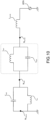
- Diagram 61 illustrates an impedance matching wire 15 made with a U-shaped metal strip connecting the supply probe 13 to the short-circuit wire 14.
- the use of a U-shaped offers a degree of freedom allowing the designer to choose the length L without modifying the position of the supply probe 13 to the short-circuit wire 14. Indeed, the distance between the supply probe 13 and the short-circuit wire 14 must remain unchanged so as not to disrupt the fundamental resonance at 2.45 GHz.
- Diagram 62 illustrates two impedance matching wires 15 each made with a metal strip in the form of a U connecting the supply probe 13 to the short-circuit wire 14.
- the two impedance matching wires are arranged symmetrically by relative to the line connecting the upper end of the supply probe 13 and that of the short-circuit wire 14.
- the two impedance matching wires have the same length L and the same width W thus forming the equivalent of a wire having a length equal to L and a width greater than 2xW.
- the use of the double metal strip offers a degree of freedom to the designer making it possible to increase the width W of the equivalent impedance matching wire without exceeding the limits in width W imposed by the constraints of the method of manufacturing the metal tracks.
- FIG 7a illustrates several variation curves of the reflection coefficient of the wire-plate antenna as a function of frequency, each curve corresponding to an electrical connection configuration of the impedance matching wire.
- Curve C0 corresponds to a wire-plate antenna without impedance matching wire 15.
- Curve C1 corresponds to a wire-plate antenna with an impedance matching wire 15 touching on one side the short-circuit wire 14 and on the other side the feed probe 13.
- the curve C2 corresponds to a wire-plate antenna with an impedance matching wire 15 touching only the wire short-circuit 14.
- Curve C3 corresponds to a wire-plate antenna with an impedance matching wire 15 touching only the supply probe 13.
- Curve C4 corresponds to a wire-plate antenna with a wire of impedance matching 15 placed close to the supply probe 13 and the short-circuit wire 14 but without touching them.
- FIG. 7b illustrates several curves of variation of the real part of the input impedance of the wire-plate antenna as a function of the frequency, each curve corresponding to an electrical connection configuration of the impedance matching wire.
- Curve C'1 corresponds to a wire-plate antenna with an impedance matching wire 15 touching on one side the short-circuit wire 14 and on the other side the feed probe 13.
- Curve C '2 corresponds to a wire-plate antenna with an impedance matching wire 15 touching only the short-circuit wire 14.
- Curve C'3 corresponds to a wire-plate antenna with an impedance matching wire 15 touching only the feeding probe 13.
- Curve C'4 corresponds to a wire-plate antenna with an impedance matching wire 15 placed close to the feeding probe 13 and the short-circuiting wire 14 but without touching them.
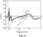
- FIG. 7c illustrates several variation curves of the imaginary part of the input impedance of the wire-plate antenna as a function of frequency, each curve corresponding to an electrical connection configuration of the impedance matching wire.
- Curve C"1 corresponds to a wire-plate antenna with an impedance matching wire 15 touching on one side the short-circuit wire 14 and on the other side the feed probe 13.
- Curve C "2 corresponds to a wire-plate antenna with an impedance matching wire 15 touching only the short-circuit wire 14.
- Curve C"3 corresponds to a wire-plate antenna with an impedance matching wire 15 touching only the feed probe 13.
- the curve C"4 corresponds to a wire-plate antenna with an impedance matching wire 15 placed close to the feed probe 13 and the short-circuit wire 14 but without touching them.
- the curve C0 corresponding to a wireless impedance matching antenna shows a reduced bandwidth BW0 around the frequency f 1 of the first low frequency monopolar resonance mode.
- the frequency range where the real part of the impedance is close to 50 ⁇ around f 1 is very small. This highlights the limitations of the wire-plate antenna without the insertion of the impedance matching wire 15 in terms of bandwidth.
- curve C1 illustrates that when the impedance matching wire 15 is connected both to the supply probe 13 and to the short-circuit wire 14, a bandwidth BW2 greater than the initial bandwidth is obtained. BW1. This bandwidth is within the target frequency range [0.5GHz,1.5GHz].
- Curve C'1 shows the appearance of a second resonance mode at a frequency f 2 around 1.1 GHz. There is also a shift of the first resonance mode to a frequency which passes from f 1 to f' 1 . The offset of the first "wire-plate resonance" mode is 100 MHz towards low frequencies.
- This phenomenon of double resonance makes it possible to create a frequency range where the impedance is stable around 50 ⁇ at the level of the real part of the input impedance between the two resonance peaks at f' 1 (associated with ⁇ ' 1 almost equal to ⁇ 1) and f 2 (associated with ⁇ 2). It is this frequency range which is exploited to widen the band. It is thus possible to widen the bandwidth of the antenna without increasing the size of the wire-plate antenna or degrading its quality factor.
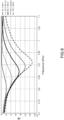
- FIG 8 illustrates several variation curves of the reflection coefficient of the wire-plate antenna as a function of frequency, each curve corresponding to a width of the impedance matching wire.
- the results of the variation of the reflection coefficient as a function of the frequency are illustrated for five values of width W of the impedance matching wire.
- the values chosen for the width W are in mm [1, 1.5, 2, 2.5, 3]. It follows that increasing the width of the wire W causes an increase in the resonance frequency because the impact of the inductive effect of the wire decreases with its width W. This parameter is useful for adjusting the imaginary part and thus adapting antenna to 50 ⁇ in the desired band.
- the results of the variation of the reflection coefficient as a function of the frequency are illustrated for four values of length L of the impedance matching wire.
- the values chosen for the length L are in mm [30, 34, 38, 42]. It follows that increasing the length of the wire L causes a decrease in the resonant frequency because the impact of the inductive effect of the wire increases with its length L. This parameter is useful for adjusting the imaginary part and thus adapting antenna to 50 ⁇ in the desired band.
- the capacitive element C roof and the inductive element L cc together form a parallel circuit L ee C roof placed between the electrical node N roof associated with the capacitive roof 12 and the electrical node N mass associated with the ground plane 11.
- the parallel circuit L cc C roof is used to excite the first resonance mode at low frequencies at f′ 1 .
- the parasitic capacitive element C par and the parasitic inductive element L par together form a parallel circuit L par C par placed between the electrical node N probe associated with the end of the implementation probe 13 and the electrical node N roof associated to the capacitive roof 12.
- the parallel circuit L by C par serves to excite the second resonance mode in the low-frequency domain at f 2 .
- the adjustment of the new resonance at f 2 can also be achieved by adding a discrete component or an adjustable component in series or parallel to the parasitic track in order to adjust the central frequency of the bandwidth obtained by the combination of f' 1 and f 2 .
- discrete component is meant a basic electronic component whose role is to perform an elementary function. In the context of the invention, this term covers passive discrete components such as inductors, capacitances, resistors.
- active LC circuits can be inserted into the structure to create resonance and widen the bandwidth. This has the advantage of a more precise control of the inductance L by .
- FIG 11 illustrates a three-dimensional radiation pattern of the wire-plate antenna according to the invention.
- the wire-plate antenna according to the invention has the advantage of omnidirectional radiation as illustrated in the figure 11 . More specifically, the figure illustrates the three-dimensional diagram of the gain achieved in the GSM band (at 917 MHz). The antenna efficiency is greater than 60% over an 80 MHz wide band corresponding to 10% of the relative band.
- FIG 12 illustrates a functional block diagram of a geolocation device comprising a wire-plate antenna according to the invention.
- the geolocation device 100 is intended to be embedded in a moving object such as a vehicle, a mobile phone, a connected watch by way of non-limiting example.
- the geolocation device comprises at least one type antenna wire-plate 10 according to the invention.
- the antenna 10 is configured to transmit to a remote server 110 via a communication system 120, the different positions of the moving object.
Applications Claiming Priority (1)
| Application Number | Priority Date | Filing Date | Title |
|---|---|---|---|
| FR2114355A FR3131463A1 (fr) | 2021-12-23 | 2021-12-23 | Antenne fil plaque monopolaire à bande passante élargie |
Publications (1)
| Publication Number | Publication Date |
|---|---|
| EP4203189A1 true EP4203189A1 (de) | 2023-06-28 |
Family
ID=81580521
Family Applications (1)
| Application Number | Title | Priority Date | Filing Date |
|---|---|---|---|
| EP22215644.0A Pending EP4203189A1 (de) | 2021-12-23 | 2022-12-21 | Monopolare patch-drahtantenne mit erweiterter bandbreite |
Country Status (3)
| Country | Link |
|---|---|
| US (1) | US20240030610A2 (de) |
| EP (1) | EP4203189A1 (de) |
| FR (1) | FR3131463A1 (de) |
Citations (4)
| Publication number | Priority date | Publication date | Assignee | Title |
|---|---|---|---|---|
| US20060256015A1 (en) * | 2005-03-16 | 2006-11-16 | Samsung Electronics Co., Ltd. | Small broadband monopole antenna having perpendicular ground plane with electromagnetically coupled feed |
| EP3235058B1 (de) | 2014-12-19 | 2020-05-27 | Commissariat à l'Énergie Atomique et aux Énergies Alternatives | Drahtplattenantenne mit einem kapazitiven dach mit einem schlitz zwischen der speisungssonde und dem kurzschlussdraht |
| US20200227829A1 (en) * | 2017-08-18 | 2020-07-16 | Sigfox | Patch antenna having two different radiation modes with two separate working frequencies, device using such an antenna |
| CN110350308B (zh) * | 2019-07-15 | 2020-12-18 | 重庆大学 | 一种超宽带低剖面垂直极化全向天线及其陷波设计方法 |
-
2021
- 2021-12-23 FR FR2114355A patent/FR3131463A1/fr active Pending
-
2022
- 2022-12-21 EP EP22215644.0A patent/EP4203189A1/de active Pending
- 2022-12-22 US US18/086,812 patent/US20240030610A2/en active Pending
Patent Citations (4)
| Publication number | Priority date | Publication date | Assignee | Title |
|---|---|---|---|---|
| US20060256015A1 (en) * | 2005-03-16 | 2006-11-16 | Samsung Electronics Co., Ltd. | Small broadband monopole antenna having perpendicular ground plane with electromagnetically coupled feed |
| EP3235058B1 (de) | 2014-12-19 | 2020-05-27 | Commissariat à l'Énergie Atomique et aux Énergies Alternatives | Drahtplattenantenne mit einem kapazitiven dach mit einem schlitz zwischen der speisungssonde und dem kurzschlussdraht |
| US20200227829A1 (en) * | 2017-08-18 | 2020-07-16 | Sigfox | Patch antenna having two different radiation modes with two separate working frequencies, device using such an antenna |
| CN110350308B (zh) * | 2019-07-15 | 2020-12-18 | 重庆大学 | 一种超宽带低剖面垂直极化全向天线及其陷波设计方法 |
Non-Patent Citations (2)
| Title |
|---|
| LAU K L ET AL: "A Wide-Band Monopolar Wire-Patch Antenna for Indoor Base Station Applications", IEEE ANTENNAS AND WIRELESS PROPAGATION LETTERS, IEEE, PISCATAWAY, NJ, US, vol. 4, no. 1, 20 June 2005 (2005-06-20), pages 155 - 157, XP011131375, ISSN: 1536-1225, DOI: 10.1109/LAWP.2005.847432 * |
| LIAO HANGUANG ET AL: "A 3D Dual-band Electrically Small Monopole Antenna for Internet of Sea Applications", 2021 IEEE INTERNATIONAL SYMPOSIUM ON ANTENNAS AND PROPAGATION AND USNC-URSI RADIO SCIENCE MEETING (APS/URSI), IEEE, 4 December 2021 (2021-12-04), pages 1 - 2, XP034084988, DOI: 10.1109/APS/URSI47566.2021.9703913 * |
Also Published As
| Publication number | Publication date |
|---|---|
| US20240030610A2 (en) | 2024-01-25 |
| US20230208038A1 (en) | 2023-06-29 |
| FR3131463A1 (fr) | 2023-06-30 |
Similar Documents
| Publication | Publication Date | Title |
|---|---|---|
| EP3669422B1 (de) | Patch-antenne mit zwei verschiedenen strahlungsmodi mit zwei getrennten arbeitsfrequenzen, vorrichtung mit einer solchen antenne | |
| EP1751820B1 (de) | Planare antenne mit leitfähigen zapfen über einer grundplatte und/oder mit mindestens einem strahlerelement und entsprechendes herstellungsverfahren | |
| EP1402596A1 (de) | Kompakte mehrbandantenne | |
| EP0604338A1 (de) | Wenig Raum beanspruchende, breitbandige Antenne mit zugehörigem Sendeempfänger | |
| WO2005036697A1 (fr) | Antenne interne de faible volume | |
| EP1576696A1 (de) | Antenne mit kleinem volumen insbesonderefür tragbare telefone | |
| EP0327965A2 (de) | Antenne für mehrere Frequenzen für Satellitenfunk | |
| EP2643886B1 (de) | Flachantenne mit erweiterter bandbreite | |
| WO1995007557A1 (fr) | Antenne fil-plaque monopolaire | |
| EP3235058B1 (de) | Drahtplattenantenne mit einem kapazitiven dach mit einem schlitz zwischen der speisungssonde und dem kurzschlussdraht | |
| FR2907969A1 (fr) | Antenne mono ou multi-frequences | |
| EP1540768B1 (de) | Helixförmige breitbandantenne | |
| EP4203189A1 (de) | Monopolare patch-drahtantenne mit erweiterter bandbreite | |
| EP1903636B1 (de) | Adaptive Breitbandantenne | |
| CN101232122B (zh) | 宽频天线 | |
| EP3031097B1 (de) | Vorrichtung zum senden und/oder empfangen von hochfrequenzsignalen | |
| FR2967537A1 (fr) | Antenne compacte adaptable en impedance | |
| FR2816114A1 (fr) | Antenne multibande | |
| EP1768212B1 (de) | Frequenzvariable Leitungsstruktur | |
| EP3942649B1 (de) | Kompakte richtantenne, vorrichtung mit einer solchen antenne | |
| FR3009431A1 (fr) | Guide d'onde rectangulaire a ondes lentes | |
| EP3537541A1 (de) | Elektromagnetische entkoppelung | |
| EP1184934A1 (de) | Planarantenne | |
| EP0578561A1 (de) | Empfänger mit innerer Ferritantenne | |
| FR2958805A1 (fr) | Antenne planaire compacte |
Legal Events
| Date | Code | Title | Description |
|---|---|---|---|
| PUAI | Public reference made under article 153(3) epc to a published international application that has entered the european phase |
Free format text: ORIGINAL CODE: 0009012 |
|
| STAA | Information on the status of an ep patent application or granted ep patent |
Free format text: STATUS: REQUEST FOR EXAMINATION WAS MADE |
|
| 17P | Request for examination filed |
Effective date: 20221221 |
|
| AK | Designated contracting states |
Kind code of ref document: A1 Designated state(s): AL AT BE BG CH CY CZ DE DK EE ES FI FR GB GR HR HU IE IS IT LI LT LU LV MC ME MK MT NL NO PL PT RO RS SE SI SK SM TR |