EP4202986B1 - Herstellung eines vias in einer integrierten schaltung - Google Patents
Herstellung eines vias in einer integrierten schaltung Download PDFInfo
- Publication number
- EP4202986B1 EP4202986B1 EP21216251.5A EP21216251A EP4202986B1 EP 4202986 B1 EP4202986 B1 EP 4202986B1 EP 21216251 A EP21216251 A EP 21216251A EP 4202986 B1 EP4202986 B1 EP 4202986B1
- Authority
- EP
- European Patent Office
- Prior art keywords
- electrically conductive
- mob
- conductive line
- dielectric layer
- top surface
- Prior art date
- Legal status (The legal status is an assumption and is not a legal conclusion. Google has not performed a legal analysis and makes no representation as to the accuracy of the status listed.)
- Active
Links
Images











Classifications
-
- H—ELECTRICITY
- H10—SEMICONDUCTOR DEVICES; ELECTRIC SOLID-STATE DEVICES NOT OTHERWISE PROVIDED FOR
- H10W—GENERIC PACKAGES, INTERCONNECTIONS, CONNECTORS OR OTHER CONSTRUCTIONAL DETAILS OF DEVICES COVERED BY CLASS H10
- H10W20/00—Interconnections in chips, wafers or substrates
- H10W20/01—Manufacture or treatment
- H10W20/031—Manufacture or treatment of conductive parts of the interconnections
- H10W20/0698—Local interconnections
-
- H—ELECTRICITY
- H10—SEMICONDUCTOR DEVICES; ELECTRIC SOLID-STATE DEVICES NOT OTHERWISE PROVIDED FOR
- H10D—INORGANIC ELECTRIC SEMICONDUCTOR DEVICES
- H10D84/00—Integrated devices formed in or on semiconductor substrates that comprise only semiconducting layers, e.g. on Si wafers or on GaAs-on-Si wafers
- H10D84/01—Manufacture or treatment
- H10D84/0123—Integrating together multiple components covered by H10D12/00 or H10D30/00, e.g. integrating multiple IGBTs
- H10D84/0126—Integrating together multiple components covered by H10D12/00 or H10D30/00, e.g. integrating multiple IGBTs the components including insulated gates, e.g. IGFETs
- H10D84/0165—Integrating together multiple components covered by H10D12/00 or H10D30/00, e.g. integrating multiple IGBTs the components including insulated gates, e.g. IGFETs the components including complementary IGFETs, e.g. CMOS devices
- H10D84/0186—Manufacturing their interconnections or electrodes, e.g. source or drain electrodes
-
- H—ELECTRICITY
- H10—SEMICONDUCTOR DEVICES; ELECTRIC SOLID-STATE DEVICES NOT OTHERWISE PROVIDED FOR
- H10D—INORGANIC ELECTRIC SEMICONDUCTOR DEVICES
- H10D84/00—Integrated devices formed in or on semiconductor substrates that comprise only semiconducting layers, e.g. on Si wafers or on GaAs-on-Si wafers
- H10D84/01—Manufacture or treatment
- H10D84/02—Manufacture or treatment characterised by using material-based technologies
- H10D84/03—Manufacture or treatment characterised by using material-based technologies using Group IV technology, e.g. silicon technology or silicon-carbide [SiC] technology
- H10D84/038—Manufacture or treatment characterised by using material-based technologies using Group IV technology, e.g. silicon technology or silicon-carbide [SiC] technology using silicon technology, e.g. SiGe
-
- H—ELECTRICITY
- H10—SEMICONDUCTOR DEVICES; ELECTRIC SOLID-STATE DEVICES NOT OTHERWISE PROVIDED FOR
- H10D—INORGANIC ELECTRIC SEMICONDUCTOR DEVICES
- H10D84/00—Integrated devices formed in or on semiconductor substrates that comprise only semiconducting layers, e.g. on Si wafers or on GaAs-on-Si wafers
- H10D84/80—Integrated devices formed in or on semiconductor substrates that comprise only semiconducting layers, e.g. on Si wafers or on GaAs-on-Si wafers characterised by the integration of at least one component covered by groups H10D12/00 or H10D30/00, e.g. integration of IGFETs
- H10D84/82—Integrated devices formed in or on semiconductor substrates that comprise only semiconducting layers, e.g. on Si wafers or on GaAs-on-Si wafers characterised by the integration of at least one component covered by groups H10D12/00 or H10D30/00, e.g. integration of IGFETs of only field-effect components
- H10D84/83—Integrated devices formed in or on semiconductor substrates that comprise only semiconducting layers, e.g. on Si wafers or on GaAs-on-Si wafers characterised by the integration of at least one component covered by groups H10D12/00 or H10D30/00, e.g. integration of IGFETs of only field-effect components of only insulated-gate FETs [IGFET]
- H10D84/85—Complementary IGFETs, e.g. CMOS
-
- H—ELECTRICITY
- H10—SEMICONDUCTOR DEVICES; ELECTRIC SOLID-STATE DEVICES NOT OTHERWISE PROVIDED FOR
- H10D—INORGANIC ELECTRIC SEMICONDUCTOR DEVICES
- H10D84/00—Integrated devices formed in or on semiconductor substrates that comprise only semiconducting layers, e.g. on Si wafers or on GaAs-on-Si wafers
- H10D84/80—Integrated devices formed in or on semiconductor substrates that comprise only semiconducting layers, e.g. on Si wafers or on GaAs-on-Si wafers characterised by the integration of at least one component covered by groups H10D12/00 or H10D30/00, e.g. integration of IGFETs
- H10D84/82—Integrated devices formed in or on semiconductor substrates that comprise only semiconducting layers, e.g. on Si wafers or on GaAs-on-Si wafers characterised by the integration of at least one component covered by groups H10D12/00 or H10D30/00, e.g. integration of IGFETs of only field-effect components
- H10D84/83—Integrated devices formed in or on semiconductor substrates that comprise only semiconducting layers, e.g. on Si wafers or on GaAs-on-Si wafers characterised by the integration of at least one component covered by groups H10D12/00 or H10D30/00, e.g. integration of IGFETs of only field-effect components of only insulated-gate FETs [IGFET]
- H10D84/85—Complementary IGFETs, e.g. CMOS
- H10D84/851—Complementary IGFETs, e.g. CMOS comprising IGFETs having stacked nanowire, nanosheet or nanoribbon channels
- H10D84/852—Complementary IGFETs, e.g. CMOS comprising IGFETs having stacked nanowire, nanosheet or nanoribbon channels comprising forksheet IGFETs
-
- H—ELECTRICITY
- H10—SEMICONDUCTOR DEVICES; ELECTRIC SOLID-STATE DEVICES NOT OTHERWISE PROVIDED FOR
- H10W—GENERIC PACKAGES, INTERCONNECTIONS, CONNECTORS OR OTHER CONSTRUCTIONAL DETAILS OF DEVICES COVERED BY CLASS H10
- H10W20/00—Interconnections in chips, wafers or substrates
- H10W20/01—Manufacture or treatment
- H10W20/031—Manufacture or treatment of conductive parts of the interconnections
- H10W20/056—Manufacture or treatment of conductive parts of the interconnections by filling conductive material into holes, grooves or trenches
- H10W20/057—Manufacture or treatment of conductive parts of the interconnections by filling conductive material into holes, grooves or trenches by selectively depositing, e.g. by using selective CVD or plating
-
- H—ELECTRICITY
- H10—SEMICONDUCTOR DEVICES; ELECTRIC SOLID-STATE DEVICES NOT OTHERWISE PROVIDED FOR
- H10W—GENERIC PACKAGES, INTERCONNECTIONS, CONNECTORS OR OTHER CONSTRUCTIONAL DETAILS OF DEVICES COVERED BY CLASS H10
- H10W20/00—Interconnections in chips, wafers or substrates
- H10W20/01—Manufacture or treatment
- H10W20/031—Manufacture or treatment of conductive parts of the interconnections
- H10W20/069—Manufacture or treatment of conductive parts of the interconnections by forming self-aligned vias or self-aligned contact plugs
-
- H—ELECTRICITY
- H10—SEMICONDUCTOR DEVICES; ELECTRIC SOLID-STATE DEVICES NOT OTHERWISE PROVIDED FOR
- H10W—GENERIC PACKAGES, INTERCONNECTIONS, CONNECTORS OR OTHER CONSTRUCTIONAL DETAILS OF DEVICES COVERED BY CLASS H10
- H10W20/00—Interconnections in chips, wafers or substrates
- H10W20/01—Manufacture or treatment
- H10W20/031—Manufacture or treatment of conductive parts of the interconnections
- H10W20/069—Manufacture or treatment of conductive parts of the interconnections by forming self-aligned vias or self-aligned contact plugs
- H10W20/0693—Manufacture or treatment of conductive parts of the interconnections by forming self-aligned vias or self-aligned contact plugs by forming self-aligned vias
-
- H—ELECTRICITY
- H10—SEMICONDUCTOR DEVICES; ELECTRIC SOLID-STATE DEVICES NOT OTHERWISE PROVIDED FOR
- H10W—GENERIC PACKAGES, INTERCONNECTIONS, CONNECTORS OR OTHER CONSTRUCTIONAL DETAILS OF DEVICES COVERED BY CLASS H10
- H10W20/00—Interconnections in chips, wafers or substrates
- H10W20/01—Manufacture or treatment
- H10W20/071—Manufacture or treatment of dielectric parts thereof
- H10W20/074—Manufacture or treatment of dielectric parts thereof of dielectric parts comprising thin functional dielectric layers, e.g. dielectric etch-stop, barrier, capping or liner layers
- H10W20/077—Manufacture or treatment of dielectric parts thereof of dielectric parts comprising thin functional dielectric layers, e.g. dielectric etch-stop, barrier, capping or liner layers on sidewalls or on top surfaces of conductors
-
- H—ELECTRICITY
- H10—SEMICONDUCTOR DEVICES; ELECTRIC SOLID-STATE DEVICES NOT OTHERWISE PROVIDED FOR
- H10W—GENERIC PACKAGES, INTERCONNECTIONS, CONNECTORS OR OTHER CONSTRUCTIONAL DETAILS OF DEVICES COVERED BY CLASS H10
- H10W20/00—Interconnections in chips, wafers or substrates
- H10W20/40—Interconnections external to wafers or substrates, e.g. back-end-of-line [BEOL] metallisations or vias connecting to gate electrodes
- H10W20/41—Interconnections external to wafers or substrates, e.g. back-end-of-line [BEOL] metallisations or vias connecting to gate electrodes characterised by their conductive parts
- H10W20/42—Vias, e.g. via plugs
-
- H—ELECTRICITY
- H10—SEMICONDUCTOR DEVICES; ELECTRIC SOLID-STATE DEVICES NOT OTHERWISE PROVIDED FOR
- H10W—GENERIC PACKAGES, INTERCONNECTIONS, CONNECTORS OR OTHER CONSTRUCTIONAL DETAILS OF DEVICES COVERED BY CLASS H10
- H10W20/00—Interconnections in chips, wafers or substrates
- H10W20/01—Manufacture or treatment
- H10W20/031—Manufacture or treatment of conductive parts of the interconnections
- H10W20/056—Manufacture or treatment of conductive parts of the interconnections by filling conductive material into holes, grooves or trenches
-
- H—ELECTRICITY
- H10—SEMICONDUCTOR DEVICES; ELECTRIC SOLID-STATE DEVICES NOT OTHERWISE PROVIDED FOR
- H10W—GENERIC PACKAGES, INTERCONNECTIONS, CONNECTORS OR OTHER CONSTRUCTIONAL DETAILS OF DEVICES COVERED BY CLASS H10
- H10W20/00—Interconnections in chips, wafers or substrates
- H10W20/01—Manufacture or treatment
- H10W20/031—Manufacture or treatment of conductive parts of the interconnections
- H10W20/063—Manufacture or treatment of conductive parts of the interconnections by forming conductive members before forming protective insulating material
Definitions
- the present invention relates to the field of integrated circuits, and more in particular to a metallization scheme for forming an integrated circuit.
- the cell height remains stuck at the "five-track” level, i.e., a cell height that can vertically accommodate five tracks to access the pins.
- the present invention relates to a method for forming an integrated circuit or an intermediate (15) in the formation thereof comprising the steps of:
- the present invention relates to an integrated circuit or an intermediate in the fabrication thereof (15) obtainable by any embodiment of the first aspect.
- the present invention relates to an integrated circuit or an intermediate (15) in the fabrication of an integrated circuit comprising:
- the aspect ratio of the third electrically conductive via (VintG) is not as high as if it was formed after the eventual formation of second electrically conductive lines (Mintl), which is easier to achieve with quality and reliability.
- the deep via (VintG+V5) linking the second electrically conductive lines (Mintl) to the gate electrode is formed in two steps, each step forming a part (VintG or V5) of the deep via having a reasonable aspect ratio.
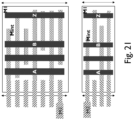
- Fig. 21 shows two examples of standard cells of the prior art having each metal track extending horizontally along the vertical axis of the cell. In a standard cell, the horizontal and vertical axes are defined with respect to the cell observed from above the substrate and oriented so that the transistor channel is oriented horizontally.
- Such cells can be referred to as HVH cells because the first level of conductive lines has its lines extending horizontally (H), and since each successive level alternates in orientation.
- the first level of conductive lines has its lines extending vertically (V).
- Such cells can, therefore, be referred to as VHV cells.
- Coupled should not be interpreted as being restricted to direct connections only.
- the terms “coupled” and “connected”, along with their derivatives, may be used. It should be understood that these terms are not intended as synonyms for each other.
- the scope of the expression “a device A coupled to a device B” should not be limited to devices or systems wherein an output of device A is directly connected to an input of device B. It means that there exists a path between an output of A and an input of B which may be a path including other devices or means.
- Coupled may mean that two or more elements are either in direct physical or electrical contact, or that two or more elements are not in direct contact with each other but yet still co-operate or interact with each other.
- an element described herein of an apparatus embodiment is an example of a means for carrying out the function performed by the element for the purpose of carrying out the invention.
- the present invention relates to a method for forming an integrated circuit or an intermediate (15) in the formation thereof comprising the steps of:
- the first electrically conductive via (VOA1) is electrically connecting the first electrically conductive line (MOB) with a first electrically conductive contact (MOA1) on a first side, here the p-type side (5p), of a first (3a) of the transistor structures (3a, 3b), while the second electrically conductive via (V0A2) is electrically connecting the first electrically conductive line (MOB) with a second electrically conductive contact (M0A2) on a first side, here an n-type side (5n), of a second (3b) of the transistor structures (3a, 3b).
- first electrically conductive via (V0A1) is electrically connecting the first electrically conductive line (MOB) with a first electrically conductive contact (MOA1) on a first side, here the n-type side (5n), of a first (3a) of the transistor structures (3a, 3b), while the second electrically conductive via (V0A2) is electrically connecting the first electrically conductive line (MOB) with a second electrically conductive contact (M0A2) on a first side, here also an n-type side (5n), of a second (3b) of the transistor structures (3a, 3b).
- first electrically conductive via (VOA1) is electrically connecting the first electrically conductive line (MOB) with a first electrically conductive contact (M0A1) on a first side, here the n-type side (5n), of a first (3a) of the transistor structures (3a, 3b), while the second electrically conductive via (V0A2) is electrically connecting the first electrically conductive line (MOB) with a second electrically conductive contact (M0A2) on a first side, here a p-type side (5p), of a second (3b) of the transistor structures (3a, 3b).
- first electrically conductive via (V0A1) is electrically connecting the first electrically conductive line (MOB) with a first electrically conductive contact (MOA1) on a first side, here the p-type side (5p), of a first (3a) of the transistor structures (3a, 3b), while the second electrically conductive via (V0A2) is electrically connecting the first electrically conductive line (MOB) with a second electrically conductive contact (M0A2) on a first side, here a p-type side (5p), of a second (3b) of the transistor structures (3a, 3b).
- step a may comprise the steps of:
- the two transistor structures (3a, 3b) may be two nanosheet transistor structures (3a, 3b), each nanosheet transistor structure comprising two nanosheet stacks, one stack forming the pMOS side (5p) of a first doping type, and another stack forming the nMOS side (5n) of a second doping type, each side (5p, 5n) comprising a plurality of vertically stacked nanosheets, said plurality forming a channel structure, a source portion, and a drain portion, the source portion and the drain portion being horizontally separated by said channel structure.
- the two transistor structures (3a, 3b) may be two transistor structures (3a, 3b), wherein the pMOS side (5p) of a first doping type and the nMOS side (5n) of a second doping type are separated by a dielectric wall (6), each side (5p, 5n) comprising a plurality of vertically stacked nanosheets, said plurality forming a channel structure, a source portion, and a drain portion, the source portion and the drain portion being horizontally separated by said channel structure, each nanosheet having one side touching said dielectric wall.
- Such transistor structures are called forksheet transistor structures. This is advantageous because it gives more space for the active devices than if nanosheets are used. Indeed, the p-n separation takes significantly less place if forksheet transistor structures (3a, 3b) are used. The reason for this is the presence of the dielectric wall (6) between the nMOS and the pMOS.
- the dielectric separation (7) may be made of SiO 2 .
- the gate may comprise a gate metal (1) such as W.
- a gate plug (4) is typically present above the gate metal (1).
- Si 3 N 4 can be used above the gate plug (4).
- Gate spacers (17) on both sides of the gate are typically present. These gate spacers (17) can for instance be made of Si 3 N 4 or silicon oxycarbide. An example of a gate structure is visible in Fig. 4 (1, 4, 17).
- the source and the drain electrically conductive contacts can for instance be SiGe:B (p-MOS) or Si:P (n-MOS).
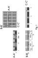
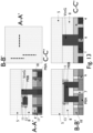
- Fig. 1 Also depicted in Fig. 1 , is the typical presence of a first active plug (18) above and in physical contact with the first electrically conductive contact (MOA1) and of a second active plug (18) above and in physical contact with the second electrically conductive contact (M0A2).
- the top surface of the active plug (18) is coplanar with the top surface of the gate spacers (17) and of the gate plug (4).
- the active plugs (18) are typically formed of a dielectric material such as SiO2. This SiO2 can, for instance, be deposited by plasma enhanced atomic layer deposition.
- the first electrically conductive line (MOB) may be embedded in a dielectric material (8).
- the first electrically conductive line is provided as part of a set of parallel first electrically conductive lines (MOB), all arranged within a first metallization level and each extending along a same first direction.
- the set of first electrically conductive lines (MOB) may be arranged at a pitch of from 20 to 60 nm, preferably, from 30 to 50 nm, more preferably from 35 to 45 nm, yet more preferably from 37 to 41 nm, and most preferably from 38 to 40 nm. This pitch being relatively large, there is enough space between the set of first electrically conductive lines (MOB) to eventually form the via (VintG) electrically connected with a gate (1).
- the planar dielectric material (8) may for instance be SiO 2 .
- each of the first electrically conductive line (MOB) and the first and second electrically conductive vias (VOA1, V0A2) may be made of a metal independently selected from metals such as Cu, Mo, Ru, or W, amongst others.
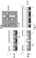
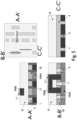
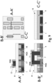
- FIG. 5 to 7 depict two alternative embodiments to perform step b.
- the protection (11) may be a dielectric protection.
- the protection (11) may be selected from dielectric materials, Cu, and Ru. Cu and Ru tend to be more resistant to the recessing conditions used in step c. In particular, it is significantly more resistant than W or Mo to fluorine-based plasma.
- step b is present, and the protection (11) may be selected from TiOx (e.g., TiO 2 ), silicon oxycarbide, silicon nitride, or even Cu or Ru if the first electrically conductive line (MOB) is made of W or Mo.
- TiOx e.g., TiO 2
- silicon oxycarbide silicon nitride
- Cu or Ru if the first electrically conductive line (MOB) is made of W or Mo.
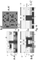
- step b is present and comprises step b1 ( Fig. 6 ) of partially recessing the first electrically conductive line (MOB), and the step b2 ( Fig. 7 ) of providing the protection (11) in the recess (24) in such a way that a top surface of the protection (11) is coplanar with a top surface of the first dielectric layer (8).
- step b is present, and comprises step b1 of partially recessing the first electrically conductive line (MOB), and the step b2 of providing the protection (11) in the recess (24) in such a way that a top surface of the protection (11) is coplanar with a top surface of the first dielectric layer (8).
- MOB first electrically conductive line
- Step b is not necessarily present because the material forming the first electrically conductive line (MOB) is different from the material forming the first dielectric layer (8), thereby allowing finding some recessing conditions with some selectivity toward the dielectric layer (8) with respect to the first electrically conductive line (M0B). If the first electrically conductive line (MOB) is W or Mo and the dielectric layer (8) is a silicon oxide, selectivity might in some case be insufficient, at least if a fluorine-based plasma is used for step c. In such a case, the protection (11) is preferably used.
- the first electrically conductive line (MOB) is Cu or Ru and the dielectric layer (8) is a silicon oxide
- selectivity with typically be sufficient if a fluorine-based plasma is used.
- the protection (11) could be used.
- Step c can for instance be performed with a fluorine-containing plasma, e.g., a SF 6 , CF 4 , CHF 3 , or C 4 F containing plasma.
- the spacers (13) may be made of silicon nitride, silicon carbon nitride, silicon carbon oxynitride, or silicon oxycarbide.
- the spacers (13) may have a thickness of from 3 to 9 nm, preferably 4 to 8 nm, more preferably 5 to 7 nm.
- the method may further comprise the following steps:
- step j may comprise:
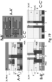
- the method may further comprise, after step m, the step n of filling the first (30) and the second interruption (31) with a dielectric material (27, Fig. 20 ).
- the method may further comprise the step o, after step m or step n, of forming:
- the method of the first aspect may be for forming a standard cell of the integrated circuit.
- the standard cell may comprise four second electrically conductive lines (Mintl) and more than four third electrically conductive lines (M1l).
- Steps l and m of etching respectively between both fourth electrically conductive vias (V4) and both fifth electrically conductive vias (V5) may be performed by any suitable method. For instance, if both fourth electrically conductive vias (V4) and both fifth electrically conductive vias (V5) are made of Ru, etching can be performed by plasma etching using Cl 2 and/or O 2 and Cl 2 as etchant gas in an inductively coupled plasma etching chamber.
- the set of second electrically conductive lines may be arranged at a pitch of from 9 to 30 nm, preferably, from 11 to 25 nm, more preferably from 14 to 22 nm, yet more preferably from 16 to 20 nm, and most preferably from 18 to 20 nm.
- the set of second electrically conductive lines (Mintl) may be arranged at a pitch and the width of the first interruption (30) as well as the width of the second interruption (31) are equal to 0.5 times the pitch.
- the distance separating both fourth electrically conductive vias (V4) may be 0.5 times the pitch of the set of second electrically conductive lines (Mintl).
- the width of each of the fourth electrically conductive vias (V4) measured along the first direction is preferably from 5 to 13 nm, more preferably from 6 to 11 nm, yet more preferably from 7 to 11 nm, and most preferably from 8 to 10 nm. Typically, the width for these two vias is 9 nm.
- the distance separating both fourth electrically conductive vias (V4) may be preferably from 5 to 13 nm, more preferably from 6 to 11 nm, yet more preferably from 7 to 11 nm, and most preferably from 8 to 10 nm. Typically, these two vias are separated by 9 nm.
- the first (30) and the second interruption (31) may each have a width of from 5 to 13 run, more preferably from 6 to 11 nm, yet more preferably from 7 to 11 nm, and most preferably from 8 to 10 nm. Typically, these interruptions have a width of 9 nm. Such a small interruption, let alone with perfect alignment to the gap, has up to now been very challenging. It is, however, easily achieved with the method of the present invention.
- the present invention relates to an integrated circuit or an intermediate (15) in the fabrication thereof obtainable by any embodiment of the first aspect.
- the present invention relates to an integrated circuit or an intermediate (15) in the fabrication of an integrated circuit comprising:
- the first electrically conductive line (MOB) extends above at least part of each transistor structure (3a, 3b) and the spacers (13) are along each sidewall of the first electrically conductive line (M0B). This is the case at least in Figs. 12 to 17 . In other embodiments corresponding for instance to Figs.
- the first electrically conductive line (MOB) comprises two parts separated by a first interruption (30) within the first electrically conductive line (MOB), a first part extending above at least part of a first transistor structure (3a) and a second part extending above at least part of a second transistor structure (3b), thereby electrically separating the first electrically conductive via (VOA1) from the second electrically conductive via (V0A2), and the spacers are along each sidewall of each part of the first electrically conductive line (MOB) except along the sidewalls facing the interruption (30).
- the first electrically conductive line (MOB) may comprise a gap cutting the first electrically conductive line (MOB) in two, thereby electrically separating the first electrically conductive via (VOA1) from the second electrically conductive via (V0A2).
Landscapes
- Metal-Oxide And Bipolar Metal-Oxide Semiconductor Integrated Circuits (AREA)
- Internal Circuitry In Semiconductor Integrated Circuit Devices (AREA)
- Semiconductor Integrated Circuits (AREA)
Claims (15)
- Ein Verfahren zur Bildung einer integrierten Schaltung oder eines Zwischenprodukts (15) bei deren Herstellung, das die folgenden Schritte umfasst:a.- Bereitstellen einer Halbleiterstruktur (16), umfassend:i.- zwei Transistorstrukturen (3a, 3b), die durch eine dielektrische Trennung (7) getrennt sind, wobei jede Transistorstruktur (3a, 3b) eine pMOS-Seite (5p) eines ersten Dotierungstyps und eine nMOS-Seite (5n) eines zweiten Dotierungstyps umfasst, wobei jede Seite eine Kanalstruktur, einen Quellenabschnitt und einen Abflussabschnitt bildet, wobei der Quellenabschnitt und der Abflussabschnitt horizontal durch die Kanalstruktur getrennt sind,ii.- eine Gate-Struktur auf der Kanalstruktur, wobei die Gate-Struktur eine Gate-Elektrode (1) und einen Gate-Stopfen (4) umfasst,iii.- elektrisch leitende Kontakte (MOA), die mit dem Quellenabschnitt und dem Abflussabschnitt jeder Seite (5p, 5n) einer jeden Transistorstruktur (3a, 3b) elektrisch gekoppelt sind,iv.- eine erste dielektrische Schicht (8) über den beiden Transistorstrukturen (3a, 3b), der Gate-Struktur und den elektrisch leitenden Kontakten (MOA),v.- eine erste elektrisch leitende Leitung (MOB), die in der ersten dielektrischen Schicht (8) eingebettet ist, sodass eine Oberseite (19) der ersten elektrisch leitenden Leitung (MOB) und eine Oberseite (20) der ersten dielektrischen Schicht (8) koplanar sind, wobei die erste elektrisch leitende Leitung (MOB) innerhalb einer ersten Metallisierungsebene angeordnet ist und sich entlang einer ersten Richtung erstreckt, wobei sich die erste elektrisch leitende Leitung (MOB) über zumindest einen Teil jeder Transistorstruktur (3a, 3b) erstreckt,vi.- ein erstes elektrisch leitendes Durchgangsloch (VOA1), das die erste elektrisch leitende Leitung (MOB) mit einem ersten elektrisch leitenden Kontakt (MOA1) auf einer ersten Seite (5n, 5p) einer ersten (3a) der Transistorstrukturen (3a, 3b) elektrisch verbindet,vii.- ein zweites elektrisch leitendes Durchgangsloch (V0A2), das die erste elektrisch leitende Leitung (MOB) mit einem zweiten elektrisch leitenden Kontakt (M0A2) auf einer ersten Seite (5n, 5p) einer zweiten (3b) der Transistorstrukturen (3a, 3b) elektrisch verbindet,b.- gegebenenfalls Bereitstellen eines Schutzes (11) selektiv auf einer Oberseite der ersten elektrisch leitenden Leitung (MOB),c.- Aussparung der ersten dielektrischen Schicht (8), um einen oberen Abschnitt (2) aller Seitenwände der ersten elektrisch leitenden Leitung (MOB) freizulegen,d.- Bereitstellen von Abstandshaltern (13) entlang jeder Seitenwand der ersten elektrisch leitenden Leitung (MOB),e.- Aufbringen einer zweiten dielektrischen Schicht (10) auf die erste dielektrische Schicht (8), sodass eine Oberseite der Abstandshalter (13), eine Oberseite des Schutzes (11), falls vorhanden, eine Oberseite der ersten elektrisch leitenden Leitung (MOB), falls kein Schutz (11) vorhanden ist, und eine Oberseite der zweiten dielektrischen Schicht (10) koplanar sind,f.- Ätzen durch das zweite (10), das erste dielektrische Material (8) und den Gate-Stopfen (4) unter Verwendung mindestens eines der Abstandshalter (13) als Maske, wodurch eine Öffnung (28) gebildet wird, die eine Oberseite der Gate-Elektrode (1) freilegt, undg.- Bereitstellen eines elektrisch leitenden Materials (14) in der Öffnung (28), wodurch ein drittes elektrisch leitendes Durchgangsloch (VintG) gebildet wird.
- Das Verfahren nach Anspruch 1, wobei die beiden Transistorstrukturen (3a, 3b) zwei Transistorstrukturen (3a, 3b) sind, wobei die pMOS-Seite (5p) eines ersten Dotierungstyps und die nMOS-Seite (5n) eines zweiten Dotierungstyps durch eine dielektrische Wand (6) getrennt sind, wobei jede Seite (5p, 5n) eine Vielzahl von vertikal gestapelten Nanoblättern umfasst, wobei die Vielzahl eine Kanalstruktur, einen Quellenabschnitt und einen Abflussabschnitt bildet, wobei der Quellenabschnitt und der Abflussabschnitt horizontal durch die Kanalstruktur getrennt sind, wobei jedes Nanoblatt mit einer Seite die dielektrische Wand (6) berührt.
- Das Verfahren nach einem der vorstehenden Ansprüche, wobei Schritt a die folgenden Schritte umfasst:a1.- Bereitstellen einer Halbleiterstruktur, umfassend:(i)- zwei Transistorstrukturen (3a, 3b), die durch eine dielektrische Trennung (7) getrennt sind, wobei jede Transistorstruktur (3a, 3b) eine pMOS-Seite (5p) eines ersten Dotierungstyps und eine nMOS-Seite (5n) eines zweiten Dotierungstyps umfasst, wobei jede Seite eine Kanalstruktur, einen Quellenabschnitt und einen Abflussabschnitt bildet, wobei der Quellenabschnitt und der Abflussabschnitt horizontal durch die Kanalstruktur getrennt sind,(ii)- eine Gate-Struktur auf der Kanalstruktur, wobei die Gate-Struktur eine Gate-Elektrode (1) und einen Gate-Stopfen (4) umfasst, und(iii)- elektrisch leitende Kontakte (MOA), die mit dem Quellenabschnitt und dem Abflussabschnitt jeder Seite (5p, 5n) einer jeden Transistorstruktur (3a, 3b) elektrisch gekoppelt sind,a2.- Bereitstellen einer ersten dielektrischen Schicht (8) über den beiden Transistorstrukturen (3a, 3b), der Gate-Struktur und den elektrisch leitenden Kontakten (MOA),a3.- Bereitstellen einer ersten Hartmaske (9) über der ersten dielektrischen Schicht (8), wobei die erste Hartmaske (9) eine Öffnung (22) aufweist, deren Länge sich entlang einer ersten Richtung erstreckt, wobei sich die Öffnung (22) über zumindest einen Teil jeder Transistorstruktur (3a, 3b) erstreckt,a4.- Teilweises Ätzen durch die erste dielektrische Schicht (8) unter Verwendung der ersten Hartmaske (9) als Maske, wodurch ein Graben (21) gebildet wird, dessen Boden von der ersten dielektrischen Schicht (8) gebildet wird,a5.- Bedecken eines mittleren Abschnitts des Bodens mit einer zweiten Hartmaske und Ätzen von zwei Löchern (23), eines auf jeder Seite der zweiten Hartmaske, unter Verwendung der ersten und zweiten Hartmaske als Masken, wodurch ein erster elektrisch leitender Kontakt (M0A1) und ein zweiter elektrisch leitender Kontakt (M0A2) freigelegt werden,a6.- Entfernen der ersten Hartmaske (9) und der zweiten Hartmaske, unda7.- Füllen beider Löcher (23) und des Grabens (21) mit einem elektrisch leitenden Material, wodurch eine erste elektrisch leitende Leitung (MOB), das erste elektrisch leitende Durchgangsloch (VOA1) und das zweite elektrisch leitende Durchgangsloch (V0A2) gebildet werden.
- Das Verfahren nach einem der vorstehenden Ansprüche, wobei Schritt b vorhanden ist und der Schutz (11) ein dielektrischer Schutz (11) ist.
- Das Verfahren nach Anspruch 4, wobei Schritt b vorhanden ist und der dielektrische Schutz (11) TiO2 ist.
- Das Verfahren nach einem der Ansprüche 1 bis 5, wobei Schritt b vorhanden ist und den Schritt b1 des teilweisen Aussparens der ersten elektrisch leitenden Leitung (MOB) und den Schritt b2 des Anbringens des Schutzes (11) in der Aussparung (24) derart umfasst, dass eine obere Fläche des Schutzes (11) koplanar mit einer Oberseite der ersten dielektrischen Schicht (8) ist.
- Das Verfahren nach einem der vorstehenden Ansprüche, wobei die Abstandshalter (13) aus Siliziumnitrid, Siliziumkohlenstoffnitrid, Siliziumkohlenstoffoxynitrid oder Siliziumoxycarbid hergestellt sind.
- Das Verfahren nach einem der vorstehenden Ansprüche, wobei die Abstandshalter (13) eine Dicke von 3 bis 9 nm, bevorzugt 4 bis 8 nm, bevorzugter 5 bis 7 nm aufweisen.
- Das Verfahren nach einem der vorstehenden Ansprüche, das weiter die folgenden Schritte umfasst:h.- Bereitstellen einer dritten dielektrischen Schicht (5) auf der zweiten dielektrischen Schicht (10), der Oberseite der Abstandshalter (13), einer Oberseite des dritten elektrisch leitenden Durchgangs (VintG) und entweder der Oberseite der ersten elektrisch leitenden Leitung (MOB), wenn Schritt b nicht durchgeführt wurde, oder andernfalls der Oberseite des Schutzes (11),i.- Bereitstellen einer Hartmaske (25) auf einer Oberseite der dritten dielektrischen Schicht (5), wobei die Hartmaske (25) zwei Öffnungen (29) aufweist, wobei eine Trennung (s1) zwischen beiden Öffnungen (29) kleiner ist als ein Raum (s2) zwischen dem ersten elektrisch leitenden Durchgangsloch (VOA1) und dem zweiten elektrisch leitenden Durchgangsloch (V0A2), wobei die Trennung (s1) direkt über einem Raum (s2) zwischen dem ersten elektrisch leitenden Durchgangsloch (VOA1) und dem zweiten elektrisch leitenden Durchgangsloch (V0A2) liegt, wobei sich eine der Öffnungen (29) seitlich mit dem dritten elektrisch leitenden Durchgangsloch (VintG) überlappt,j.- Ätzen durch die dritte dielektrische Schicht (5) und durch den Schutz (11), falls vorhanden, unter Verwendung der Hartmaske (25) als Maske, wodurch zwei Längsöffnungen (29) gebildet werden, die sich entlang einer zweiten Richtung, typischerweise senkrecht zur ersten Richtung, erstrecken, wobei jede der Längsöffnungen (29) die erste elektrisch leitende Leitung (MOB) und das dritte elektrisch leitende Durchgangsloch (VintG) mittels eines ersten bzw. eines zweiten Durchgangslochs freilegt, das mit den Längsöffnungen (29) in Verbindung steht,k.- Bereitstellen eines elektrisch leitenden Materials (26) in den beiden Längsöffnungen (29), wodurch Folgendes gebildet wird:- zwei zweite elektrisch leitende Leitungen (Mintl1, Mintl2), die innerhalb einer zweiten Metallisierungsebene angeordnet sind und sich entlang der zweiten Richtung erstrecken, getrennt durch die Trennung S1, und- zwei vierte elektrisch leitende Durchgangslöcher (V4), von denen eines direkt physisch mit einer der beiden zweiten elektrisch leitenden Leitungen (Mintl) und mit der ersten elektrisch leitenden Leitung (MOB) verbunden ist, während das andere direkt physisch mit der anderen der beiden zweiten elektrisch leitenden Leitungen (Mintl) und mit der ersten elektrisch leitenden Leitung (MOB) verbunden ist, und- zwei fünfte elektrisch leitende Durchgangslöcher (V5), von denen eines direkt physisch mit einer der beiden zweiten elektrisch leitenden Leitungen (Mintl) und mit dem dritten elektrisch leitenden Durchgangsloch (VintG) verbunden ist, während das andere direkt physisch mit der anderen der beiden zweiten elektrisch leitenden Leitungen (Mintl) und mit dem dritten elektrisch leitenden Durchgangsloch (VintG) verbunden ist,l.- Ätzen zwischen den beiden vierten elektrisch leitenden Durchgängen (V4) durch die gesamte Dicke der ersten elektrisch leitenden Leitung (MOB) unter Verwendung der beiden vierten elektrisch leitenden Durchgangslöcher als Masken, wodurch die erste elektrisch leitende Leitung (MOB) geschnitten wird, wodurch eine erste Unterbrechung (30) innerhalb der ersten elektrisch leitenden Leitung (MOB) gebildet wird, undm.- Ätzen zwischen den beiden fünften elektrisch leitenden Durchgangslöchern (V5) durch die gesamte Dicke des dritten elektrisch leitenden Durchgangslochs (VintG), indem beide elektrisch leitenden Durchgangslöcher als Masken verwendet werden, wodurch das dritte elektrisch leitende Durchgangsloch (VintG) geschnitten wird, wodurch eine zweite Unterbrechung (31) innerhalb des dritten elektrisch leitenden Durchgangslochs (VintG) gebildet wird.
- Das Verfahren nach Anspruch 9, das weiter nach Schritt m den Schritt n des Füllens der ersten (30) und der zweiten Unterbrechung (31) mit einem dielektrischen Material (27) umfasst.
- Das Verfahren nach Anspruch 9 oder Anspruch 10, das weiter nach Schritt m oder Schritt n den Schritt o umfasst, bei dem:(i)- oberhalb der zweiten Metallisierungsebene ein Satz dritter elektrisch leitender Leitungen (M1l) gebildet wird, die innerhalb einer dritten Metallisierungsebene angeordnet sind und sich entlang der ersten Richtung erstrecken, und(ii)- ein Durchgangsloch (V1) gebildet wird, das eine dritte elektrisch leitende Leitung (M1l) mit einer zweiten elektrisch leitenden Leitung (Mintl) elektrisch verbindet.
- Das Verfahren nach einem der Ansprüche 1 bis 11 zur Bildung einer Standardzelle der integrierten Schaltung.
- Das Verfahren nach Anspruch 12 in Abhängigkeit von Anspruch 11, wobei die Standardzelle vier zweite elektrisch leitende Leitungen (Mintl) und mehr als vier dritte elektrisch leitende Leitungen (M1l) umfasst.
- Eine integrierte Schaltung oder ein Zwischenprodukt (15) bei der Herstellung einer integrierten Schaltung, umfassend:a.- eine Halbleiterstruktur (16), umfassend:i.- zwei Transistorstrukturen (3a, 3b), die durch eine dielektrische Trennung (7) getrennt sind, wobei jede Transistorstruktur (3a, 3b) eine pMOS-Seite (5p) eines ersten Dotierungstyps und eine nMOS-Seite (5n) eines zweiten Dotierungstyps umfasst, wobei jede Seite eine Kanalstruktur, einen Quellenabschnitt und einen Abflussabschnitt bildet, wobei der Quellenabschnitt und der Abflussabschnitt horizontal durch die Kanalstruktur getrennt sind,ii.- eine Gate-Struktur auf der Kanalstruktur, wobei die Gate-Struktur eine Gate-Elektrode (1) umfasst,iii.- elektrisch leitende Kontakte (MOA), die mit dem Quellenabschnitt und dem Abflussabschnitt jeder Seite (5p, 5n) einer jeden Transistorstruktur (3a, 3b) elektrisch gekoppelt sind,iv.- eine erste dielektrische Schicht (8) über den beiden Transistorstrukturen (3a, 3b), der Gate-Struktur und den elektrisch leitenden Kontakten (MOA),v.- eine erste elektrisch leitende Leitung (MOB), die in der ersten dielektrischen Schicht (8) eingebettet ist, wobei die erste elektrisch leitende Leitung (MOB) innerhalb einer ersten Metallisierungsebene angeordnet ist und sich entlang einer ersten Richtung erstreckt,vi.- ein erstes elektrisch leitendes Durchgangsloch (VOA1), das die erste elektrisch leitende Leitung (MOB) mit einem ersten elektrisch leitenden Kontakt (MOA1) auf einer ersten Seite (5n, 5p) einer ersten (3a) der Transistorstrukturen (3a, 3b) elektrisch verbindet,vii.- ein zweites elektrisch leitendes Durchgangsloch (V0A2), das die erste elektrisch leitende Leitung (MOB) mit einem zweiten elektrisch leitenden Kontakt (M0A2) auf einer ersten Seite (5n, 5p) einer zweiten (3b) der Transistorstrukturen (3a, 3b) elektrisch verbindet,viii.- Abstandshalter (13) entlang Seitenwände der ersten elektrisch leitenden Leitung (MOB),ix.- ein drittes elektrisch leitendes Durchgangsloch (VintG), die durch das zweite (10) und erste dielektrische Material (8) verläuft und einen Abstandshalter (13) und die Gate-Elektrode (1) berührt.
- Eine integrierte Schaltung oder ein Zwischenprodukt (15) bei der Herstellung einer integrierten Schaltung nach Anspruch 14, wobei entweder:a.- die erste elektrisch leitende Leitung (MOB) sich über mindestens einen Teil jeder Transistorstruktur (3a, 3b) erstreckt und die Abstandshalter (13) sich entlang jeder Seitenwand der ersten elektrisch leitenden Leitung (MOB) befinden, oderb.- die erste elektrisch leitende Leitung (MOB) zwei Teile umfasst, die durch eine erste Unterbrechung (30) innerhalb der ersten elektrisch leitenden Leitung (MOB) getrennt sind, wobei sich ein erster Teil über mindestens einen Teil einer ersten Transistorstruktur (3a) und ein zweiter Teil über mindestens einen Teil einer zweiten Transistorstruktur (3b) erstreckt, wodurch das erste elektrisch leitende Durchgangsloch (VOA1) von dem zweiten elektrisch leitenden Durchgangsloch (V0A2) elektrisch getrennt wird, und die Abstandshalter sich entlang jeder Seitenwand jedes Teils der ersten elektrisch leitenden Leitung (MOB) befinden, außer entlang der Seitenwände, die der Unterbrechung (30) gegenüberliegen.
Priority Applications (3)
| Application Number | Priority Date | Filing Date | Title |
|---|---|---|---|
| EP21216251.5A EP4202986B1 (de) | 2021-12-21 | 2021-12-21 | Herstellung eines vias in einer integrierten schaltung |
| US18/054,228 US12519015B2 (en) | 2021-12-21 | 2022-11-10 | Conductive via formation connecting transistor structures in an integrated circuit |
| CN202211550672.0A CN116314009A (zh) | 2021-12-21 | 2022-12-05 | 集成电路中的通孔形成 |
Applications Claiming Priority (1)
| Application Number | Priority Date | Filing Date | Title |
|---|---|---|---|
| EP21216251.5A EP4202986B1 (de) | 2021-12-21 | 2021-12-21 | Herstellung eines vias in einer integrierten schaltung |
Publications (2)
| Publication Number | Publication Date |
|---|---|
| EP4202986A1 EP4202986A1 (de) | 2023-06-28 |
| EP4202986B1 true EP4202986B1 (de) | 2024-05-01 |
Family
ID=78957700
Family Applications (1)
| Application Number | Title | Priority Date | Filing Date |
|---|---|---|---|
| EP21216251.5A Active EP4202986B1 (de) | 2021-12-21 | 2021-12-21 | Herstellung eines vias in einer integrierten schaltung |
Country Status (3)
| Country | Link |
|---|---|
| US (1) | US12519015B2 (de) |
| EP (1) | EP4202986B1 (de) |
| CN (1) | CN116314009A (de) |
Families Citing this family (1)
| Publication number | Priority date | Publication date | Assignee | Title |
|---|---|---|---|---|
| EP4199052B1 (de) * | 2021-12-17 | 2024-08-21 | IMEC vzw | Metallisierungsschema für eine integrierte schaltung |
Family Cites Families (3)
| Publication number | Priority date | Publication date | Assignee | Title |
|---|---|---|---|---|
| KR101923120B1 (ko) * | 2012-03-21 | 2018-11-28 | 삼성전자 주식회사 | 반도체 소자 및 이의 제조 방법 |
| US20160005822A1 (en) * | 2014-07-01 | 2016-01-07 | Qualcomm Incorporated | Self-aligned via for gate contact of semiconductor devices |
| US10497612B2 (en) * | 2017-12-11 | 2019-12-03 | Globalfoundries Inc. | Methods of forming contact structures on integrated circuit products |
-
2021
- 2021-12-21 EP EP21216251.5A patent/EP4202986B1/de active Active
-
2022
- 2022-11-10 US US18/054,228 patent/US12519015B2/en active Active
- 2022-12-05 CN CN202211550672.0A patent/CN116314009A/zh active Pending
Also Published As
| Publication number | Publication date |
|---|---|
| CN116314009A (zh) | 2023-06-23 |
| US12519015B2 (en) | 2026-01-06 |
| US20230197528A1 (en) | 2023-06-22 |
| EP4202986A1 (de) | 2023-06-28 |
Similar Documents
| Publication | Publication Date | Title |
|---|---|---|
| CN112103291B (zh) | 具有埋置交叉耦接互连的结构及sram位单元 | |
| US11810981B2 (en) | Semiconductor structure having both gate-all-around devices and planar devices | |
| US12243913B2 (en) | Self-aligned backside contact integration for transistors | |
| US11244949B2 (en) | Semiconductor device having stacked transistor pairs and method of forming same | |
| US20230197514A1 (en) | Metallization Process for an Integrated Circuit | |
| US8916441B2 (en) | FinFET device and methods of fabrication | |
| US10424577B2 (en) | Semiconductor devices | |
| US20050104130A1 (en) | High-density split-gate FinFET | |
| TW201907486A (zh) | 積體電路元件及其製造方法 | |
| US7223650B2 (en) | Self-aligned gate isolation | |
| US20240006313A1 (en) | Self-aligned backside connections for transistors | |
| US12519015B2 (en) | Conductive via formation connecting transistor structures in an integrated circuit | |
| CN218004863U (zh) | 半导体装置 | |
| CN112216695A (zh) | 半导体装置及形成半导体装置的方法 | |
| US11521971B2 (en) | Gate dielectric having a non-uniform thickness profile | |
| US20250176256A1 (en) | Bridge structure for different threshold-voltage devices | |
| KR102533938B1 (ko) | 3 차원 메모리 디바이스 및 형성 방법 | |
| JP2025502153A (ja) | 集積回路内のディフュージョンブレイクにおける配線 | |
| US20230386929A1 (en) | Semiconductor structure and fabrication method thereof | |
| US20240213312A1 (en) | Integrated Circuit Devices and Methods for Making Such Devices | |
| US20260026088A1 (en) | Area scaling using an extended full cut with a supporting backside gate jumper | |
| US20250351567A1 (en) | Three-dimensional stacked semiconductor device including simplified source/drain contact area | |
| US20240306379A1 (en) | Semiconductor device | |
| WO2026090983A1 (en) | Semiconductor devices and methods for forming the same | |
| KR20260061129A (ko) | 수직 채널 트랜지스터들을 포함하는 반도체 장치 |
Legal Events
| Date | Code | Title | Description |
|---|---|---|---|
| PUAI | Public reference made under article 153(3) epc to a published international application that has entered the european phase |
Free format text: ORIGINAL CODE: 0009012 |
|
| STAA | Information on the status of an ep patent application or granted ep patent |
Free format text: STATUS: THE APPLICATION HAS BEEN PUBLISHED |
|
| AK | Designated contracting states |
Kind code of ref document: A1 Designated state(s): AL AT BE BG CH CY CZ DE DK EE ES FI FR GB GR HR HU IE IS IT LI LT LU LV MC MK MT NL NO PL PT RO RS SE SI SK SM TR |
|
| STAA | Information on the status of an ep patent application or granted ep patent |
Free format text: STATUS: REQUEST FOR EXAMINATION WAS MADE |
|
| 17P | Request for examination filed |
Effective date: 20231023 |
|
| RBV | Designated contracting states (corrected) |
Designated state(s): AL AT BE BG CH CY CZ DE DK EE ES FI FR GB GR HR HU IE IS IT LI LT LU LV MC MK MT NL NO PL PT RO RS SE SI SK SM TR |
|
| GRAP | Despatch of communication of intention to grant a patent |
Free format text: ORIGINAL CODE: EPIDOSNIGR1 |
|
| STAA | Information on the status of an ep patent application or granted ep patent |
Free format text: STATUS: GRANT OF PATENT IS INTENDED |
|
| INTG | Intention to grant announced |
Effective date: 20240123 |
|
| RAP3 | Party data changed (applicant data changed or rights of an application transferred) |
Owner name: IMEC VZW |
|
| P01 | Opt-out of the competence of the unified patent court (upc) registered |
Effective date: 20240208 |
|
| GRAS | Grant fee paid |
Free format text: ORIGINAL CODE: EPIDOSNIGR3 |
|
| GRAA | (expected) grant |
Free format text: ORIGINAL CODE: 0009210 |
|
| STAA | Information on the status of an ep patent application or granted ep patent |
Free format text: STATUS: THE PATENT HAS BEEN GRANTED |
|
| AK | Designated contracting states |
Kind code of ref document: B1 Designated state(s): AL AT BE BG CH CY CZ DE DK EE ES FI FR GB GR HR HU IE IS IT LI LT LU LV MC MK MT NL NO PL PT RO RS SE SI SK SM TR |
|
| REG | Reference to a national code |
Ref country code: GB Ref legal event code: FG4D |
|
| REG | Reference to a national code |
Ref country code: CH Ref legal event code: EP |
|
| REG | Reference to a national code |
Ref country code: IE Ref legal event code: FG4D |
|
| REG | Reference to a national code |
Ref country code: DE Ref legal event code: R096 Ref document number: 602021012640 Country of ref document: DE |
|
| REG | Reference to a national code |
Ref country code: LT Ref legal event code: MG9D |
|
| REG | Reference to a national code |
Ref country code: NL Ref legal event code: MP Effective date: 20240501 |
|
| PG25 | Lapsed in a contracting state [announced via postgrant information from national office to epo] |
Ref country code: IS Free format text: LAPSE BECAUSE OF FAILURE TO SUBMIT A TRANSLATION OF THE DESCRIPTION OR TO PAY THE FEE WITHIN THE PRESCRIBED TIME-LIMIT Effective date: 20240901 |
|
| PG25 | Lapsed in a contracting state [announced via postgrant information from national office to epo] |
Ref country code: BG Free format text: LAPSE BECAUSE OF FAILURE TO SUBMIT A TRANSLATION OF THE DESCRIPTION OR TO PAY THE FEE WITHIN THE PRESCRIBED TIME-LIMIT Effective date: 20240501 |
|
| PG25 | Lapsed in a contracting state [announced via postgrant information from national office to epo] |
Ref country code: FI Free format text: LAPSE BECAUSE OF FAILURE TO SUBMIT A TRANSLATION OF THE DESCRIPTION OR TO PAY THE FEE WITHIN THE PRESCRIBED TIME-LIMIT Effective date: 20240501 Ref country code: HR Free format text: LAPSE BECAUSE OF FAILURE TO SUBMIT A TRANSLATION OF THE DESCRIPTION OR TO PAY THE FEE WITHIN THE PRESCRIBED TIME-LIMIT Effective date: 20240501 |
|
| PG25 | Lapsed in a contracting state [announced via postgrant information from national office to epo] |
Ref country code: GR Free format text: LAPSE BECAUSE OF FAILURE TO SUBMIT A TRANSLATION OF THE DESCRIPTION OR TO PAY THE FEE WITHIN THE PRESCRIBED TIME-LIMIT Effective date: 20240802 |
|
| PG25 | Lapsed in a contracting state [announced via postgrant information from national office to epo] |
Ref country code: PT Free format text: LAPSE BECAUSE OF FAILURE TO SUBMIT A TRANSLATION OF THE DESCRIPTION OR TO PAY THE FEE WITHIN THE PRESCRIBED TIME-LIMIT Effective date: 20240902 |
|
| REG | Reference to a national code |
Ref country code: AT Ref legal event code: MK05 Ref document number: 1683597 Country of ref document: AT Kind code of ref document: T Effective date: 20240501 |
|
| PG25 | Lapsed in a contracting state [announced via postgrant information from national office to epo] |
Ref country code: NL Free format text: LAPSE BECAUSE OF FAILURE TO SUBMIT A TRANSLATION OF THE DESCRIPTION OR TO PAY THE FEE WITHIN THE PRESCRIBED TIME-LIMIT Effective date: 20240501 |
|
| PG25 | Lapsed in a contracting state [announced via postgrant information from national office to epo] |
Ref country code: ES Free format text: LAPSE BECAUSE OF FAILURE TO SUBMIT A TRANSLATION OF THE DESCRIPTION OR TO PAY THE FEE WITHIN THE PRESCRIBED TIME-LIMIT Effective date: 20240501 |
|
| PG25 | Lapsed in a contracting state [announced via postgrant information from national office to epo] |
Ref country code: AT Free format text: LAPSE BECAUSE OF FAILURE TO SUBMIT A TRANSLATION OF THE DESCRIPTION OR TO PAY THE FEE WITHIN THE PRESCRIBED TIME-LIMIT Effective date: 20240501 |
|
| PG25 | Lapsed in a contracting state [announced via postgrant information from national office to epo] |
Ref country code: PL Free format text: LAPSE BECAUSE OF FAILURE TO SUBMIT A TRANSLATION OF THE DESCRIPTION OR TO PAY THE FEE WITHIN THE PRESCRIBED TIME-LIMIT Effective date: 20240501 |
|
| PG25 | Lapsed in a contracting state [announced via postgrant information from national office to epo] |
Ref country code: LV Free format text: LAPSE BECAUSE OF FAILURE TO SUBMIT A TRANSLATION OF THE DESCRIPTION OR TO PAY THE FEE WITHIN THE PRESCRIBED TIME-LIMIT Effective date: 20240501 |
|
| PG25 | Lapsed in a contracting state [announced via postgrant information from national office to epo] |
Ref country code: PT Free format text: LAPSE BECAUSE OF FAILURE TO SUBMIT A TRANSLATION OF THE DESCRIPTION OR TO PAY THE FEE WITHIN THE PRESCRIBED TIME-LIMIT Effective date: 20240902 Ref country code: PL Free format text: LAPSE BECAUSE OF FAILURE TO SUBMIT A TRANSLATION OF THE DESCRIPTION OR TO PAY THE FEE WITHIN THE PRESCRIBED TIME-LIMIT Effective date: 20240501 Ref country code: NO Free format text: LAPSE BECAUSE OF FAILURE TO SUBMIT A TRANSLATION OF THE DESCRIPTION OR TO PAY THE FEE WITHIN THE PRESCRIBED TIME-LIMIT Effective date: 20240801 Ref country code: NL Free format text: LAPSE BECAUSE OF FAILURE TO SUBMIT A TRANSLATION OF THE DESCRIPTION OR TO PAY THE FEE WITHIN THE PRESCRIBED TIME-LIMIT Effective date: 20240501 Ref country code: LV Free format text: LAPSE BECAUSE OF FAILURE TO SUBMIT A TRANSLATION OF THE DESCRIPTION OR TO PAY THE FEE WITHIN THE PRESCRIBED TIME-LIMIT Effective date: 20240501 Ref country code: IS Free format text: LAPSE BECAUSE OF FAILURE TO SUBMIT A TRANSLATION OF THE DESCRIPTION OR TO PAY THE FEE WITHIN THE PRESCRIBED TIME-LIMIT Effective date: 20240901 Ref country code: HR Free format text: LAPSE BECAUSE OF FAILURE TO SUBMIT A TRANSLATION OF THE DESCRIPTION OR TO PAY THE FEE WITHIN THE PRESCRIBED TIME-LIMIT Effective date: 20240501 Ref country code: GR Free format text: LAPSE BECAUSE OF FAILURE TO SUBMIT A TRANSLATION OF THE DESCRIPTION OR TO PAY THE FEE WITHIN THE PRESCRIBED TIME-LIMIT Effective date: 20240802 Ref country code: FI Free format text: LAPSE BECAUSE OF FAILURE TO SUBMIT A TRANSLATION OF THE DESCRIPTION OR TO PAY THE FEE WITHIN THE PRESCRIBED TIME-LIMIT Effective date: 20240501 Ref country code: ES Free format text: LAPSE BECAUSE OF FAILURE TO SUBMIT A TRANSLATION OF THE DESCRIPTION OR TO PAY THE FEE WITHIN THE PRESCRIBED TIME-LIMIT Effective date: 20240501 Ref country code: BG Free format text: LAPSE BECAUSE OF FAILURE TO SUBMIT A TRANSLATION OF THE DESCRIPTION OR TO PAY THE FEE WITHIN THE PRESCRIBED TIME-LIMIT Effective date: 20240501 Ref country code: AT Free format text: LAPSE BECAUSE OF FAILURE TO SUBMIT A TRANSLATION OF THE DESCRIPTION OR TO PAY THE FEE WITHIN THE PRESCRIBED TIME-LIMIT Effective date: 20240501 Ref country code: RS Free format text: LAPSE BECAUSE OF FAILURE TO SUBMIT A TRANSLATION OF THE DESCRIPTION OR TO PAY THE FEE WITHIN THE PRESCRIBED TIME-LIMIT Effective date: 20240801 |
|
| PG25 | Lapsed in a contracting state [announced via postgrant information from national office to epo] |
Ref country code: DK Free format text: LAPSE BECAUSE OF FAILURE TO SUBMIT A TRANSLATION OF THE DESCRIPTION OR TO PAY THE FEE WITHIN THE PRESCRIBED TIME-LIMIT Effective date: 20240501 |
|
| PG25 | Lapsed in a contracting state [announced via postgrant information from national office to epo] |
Ref country code: EE Free format text: LAPSE BECAUSE OF FAILURE TO SUBMIT A TRANSLATION OF THE DESCRIPTION OR TO PAY THE FEE WITHIN THE PRESCRIBED TIME-LIMIT Effective date: 20240501 |
|
| PG25 | Lapsed in a contracting state [announced via postgrant information from national office to epo] |
Ref country code: CZ Free format text: LAPSE BECAUSE OF FAILURE TO SUBMIT A TRANSLATION OF THE DESCRIPTION OR TO PAY THE FEE WITHIN THE PRESCRIBED TIME-LIMIT Effective date: 20240501 |
|
| PG25 | Lapsed in a contracting state [announced via postgrant information from national office to epo] |
Ref country code: RO Free format text: LAPSE BECAUSE OF FAILURE TO SUBMIT A TRANSLATION OF THE DESCRIPTION OR TO PAY THE FEE WITHIN THE PRESCRIBED TIME-LIMIT Effective date: 20240501 Ref country code: SK Free format text: LAPSE BECAUSE OF FAILURE TO SUBMIT A TRANSLATION OF THE DESCRIPTION OR TO PAY THE FEE WITHIN THE PRESCRIBED TIME-LIMIT Effective date: 20240501 |
|
| PG25 | Lapsed in a contracting state [announced via postgrant information from national office to epo] |
Ref country code: SM Free format text: LAPSE BECAUSE OF FAILURE TO SUBMIT A TRANSLATION OF THE DESCRIPTION OR TO PAY THE FEE WITHIN THE PRESCRIBED TIME-LIMIT Effective date: 20240501 |
|
| PG25 | Lapsed in a contracting state [announced via postgrant information from national office to epo] |
Ref country code: SM Free format text: LAPSE BECAUSE OF FAILURE TO SUBMIT A TRANSLATION OF THE DESCRIPTION OR TO PAY THE FEE WITHIN THE PRESCRIBED TIME-LIMIT Effective date: 20240501 Ref country code: SK Free format text: LAPSE BECAUSE OF FAILURE TO SUBMIT A TRANSLATION OF THE DESCRIPTION OR TO PAY THE FEE WITHIN THE PRESCRIBED TIME-LIMIT Effective date: 20240501 Ref country code: RO Free format text: LAPSE BECAUSE OF FAILURE TO SUBMIT A TRANSLATION OF THE DESCRIPTION OR TO PAY THE FEE WITHIN THE PRESCRIBED TIME-LIMIT Effective date: 20240501 Ref country code: EE Free format text: LAPSE BECAUSE OF FAILURE TO SUBMIT A TRANSLATION OF THE DESCRIPTION OR TO PAY THE FEE WITHIN THE PRESCRIBED TIME-LIMIT Effective date: 20240501 Ref country code: DK Free format text: LAPSE BECAUSE OF FAILURE TO SUBMIT A TRANSLATION OF THE DESCRIPTION OR TO PAY THE FEE WITHIN THE PRESCRIBED TIME-LIMIT Effective date: 20240501 Ref country code: CZ Free format text: LAPSE BECAUSE OF FAILURE TO SUBMIT A TRANSLATION OF THE DESCRIPTION OR TO PAY THE FEE WITHIN THE PRESCRIBED TIME-LIMIT Effective date: 20240501 |
|
| REG | Reference to a national code |
Ref country code: DE Ref legal event code: R097 Ref document number: 602021012640 Country of ref document: DE |
|
| PG25 | Lapsed in a contracting state [announced via postgrant information from national office to epo] |
Ref country code: IT Free format text: LAPSE BECAUSE OF FAILURE TO SUBMIT A TRANSLATION OF THE DESCRIPTION OR TO PAY THE FEE WITHIN THE PRESCRIBED TIME-LIMIT Effective date: 20240501 |
|
| PLBE | No opposition filed within time limit |
Free format text: ORIGINAL CODE: 0009261 |
|
| STAA | Information on the status of an ep patent application or granted ep patent |
Free format text: STATUS: NO OPPOSITION FILED WITHIN TIME LIMIT |
|
| 26N | No opposition filed |
Effective date: 20250204 |
|
| PG25 | Lapsed in a contracting state [announced via postgrant information from national office to epo] |
Ref country code: SI Free format text: LAPSE BECAUSE OF FAILURE TO SUBMIT A TRANSLATION OF THE DESCRIPTION OR TO PAY THE FEE WITHIN THE PRESCRIBED TIME-LIMIT Effective date: 20240501 |
|
| PG25 | Lapsed in a contracting state [announced via postgrant information from national office to epo] |
Ref country code: MC Free format text: LAPSE BECAUSE OF FAILURE TO SUBMIT A TRANSLATION OF THE DESCRIPTION OR TO PAY THE FEE WITHIN THE PRESCRIBED TIME-LIMIT Effective date: 20240501 |
|
| REG | Reference to a national code |
Ref country code: CH Ref legal event code: PL |
|
| PG25 | Lapsed in a contracting state [announced via postgrant information from national office to epo] |
Ref country code: LU Free format text: LAPSE BECAUSE OF NON-PAYMENT OF DUE FEES Effective date: 20241221 |
|
| PG25 | Lapsed in a contracting state [announced via postgrant information from national office to epo] |
Ref country code: SE Free format text: LAPSE BECAUSE OF FAILURE TO SUBMIT A TRANSLATION OF THE DESCRIPTION OR TO PAY THE FEE WITHIN THE PRESCRIBED TIME-LIMIT Effective date: 20240501 |
|
| REG | Reference to a national code |
Ref country code: BE Ref legal event code: MM Effective date: 20241231 |
|
| PG25 | Lapsed in a contracting state [announced via postgrant information from national office to epo] |
Ref country code: BE Free format text: LAPSE BECAUSE OF NON-PAYMENT OF DUE FEES Effective date: 20241231 |
|
| PG25 | Lapsed in a contracting state [announced via postgrant information from national office to epo] |
Ref country code: FR Free format text: LAPSE BECAUSE OF NON-PAYMENT OF DUE FEES Effective date: 20241231 |
|
| PG25 | Lapsed in a contracting state [announced via postgrant information from national office to epo] |
Ref country code: CH Free format text: LAPSE BECAUSE OF NON-PAYMENT OF DUE FEES Effective date: 20241231 |
|
| PG25 | Lapsed in a contracting state [announced via postgrant information from national office to epo] |
Ref country code: IE Free format text: LAPSE BECAUSE OF NON-PAYMENT OF DUE FEES Effective date: 20241221 |
|
| REG | Reference to a national code |
Ref country code: DE Ref legal event code: R079 Ref document number: 602021012640 Country of ref document: DE Free format text: PREVIOUS MAIN CLASS: H01L0021768000 Ipc: H10W0020000000 |
|
| PGFP | Annual fee paid to national office [announced via postgrant information from national office to epo] |
Ref country code: DE Payment date: 20251126 Year of fee payment: 5 |