EP4199126B1 - Herstellung von perowskitbasierten optoelektronischen vorrichtungen - Google Patents
Herstellung von perowskitbasierten optoelektronischen vorrichtungen Download PDFInfo
- Publication number
- EP4199126B1 EP4199126B1 EP21215793.7A EP21215793A EP4199126B1 EP 4199126 B1 EP4199126 B1 EP 4199126B1 EP 21215793 A EP21215793 A EP 21215793A EP 4199126 B1 EP4199126 B1 EP 4199126B1
- Authority
- EP
- European Patent Office
- Prior art keywords
- layer
- stack
- sputtering
- layers
- type semiconducting
- Prior art date
- Legal status (The legal status is an assumption and is not a legal conclusion. Google has not performed a legal analysis and makes no representation as to the accuracy of the status listed.)
- Active
Links
Images




Classifications
-
- H—ELECTRICITY
- H10—SEMICONDUCTOR DEVICES; ELECTRIC SOLID-STATE DEVICES NOT OTHERWISE PROVIDED FOR
- H10K—ORGANIC ELECTRIC SOLID-STATE DEVICES
- H10K85/00—Organic materials used in the body or electrodes of devices covered by this subclass
- H10K85/50—Organic perovskites; Hybrid organic-inorganic perovskites [HOIP], e.g. CH3NH3PbI3
-
- H—ELECTRICITY
- H01—ELECTRIC ELEMENTS
- H01G—CAPACITORS; CAPACITORS, RECTIFIERS, DETECTORS, SWITCHING DEVICES, LIGHT-SENSITIVE OR TEMPERATURE-SENSITIVE DEVICES OF THE ELECTROLYTIC TYPE
- H01G9/00—Electrolytic capacitors, rectifiers, detectors, switching devices, light-sensitive or temperature-sensitive devices; Processes of their manufacture
- H01G9/0029—Processes of manufacture
- H01G9/0036—Formation of the solid electrolyte layer
-
- H—ELECTRICITY
- H01—ELECTRIC ELEMENTS
- H01G—CAPACITORS; CAPACITORS, RECTIFIERS, DETECTORS, SWITCHING DEVICES, LIGHT-SENSITIVE OR TEMPERATURE-SENSITIVE DEVICES OF THE ELECTROLYTIC TYPE
- H01G9/00—Electrolytic capacitors, rectifiers, detectors, switching devices, light-sensitive or temperature-sensitive devices; Processes of their manufacture
- H01G9/20—Light-sensitive devices
- H01G9/2004—Light-sensitive devices characterised by the electrolyte, e.g. comprising an organic electrolyte
- H01G9/2009—Solid electrolytes
-
- H—ELECTRICITY
- H10—SEMICONDUCTOR DEVICES; ELECTRIC SOLID-STATE DEVICES NOT OTHERWISE PROVIDED FOR
- H10K—ORGANIC ELECTRIC SOLID-STATE DEVICES
- H10K30/00—Organic devices sensitive to infrared radiation, light, electromagnetic radiation of shorter wavelength or corpuscular radiation
- H10K30/20—Organic devices sensitive to infrared radiation, light, electromagnetic radiation of shorter wavelength or corpuscular radiation comprising organic-organic junctions, e.g. donor-acceptor junctions
-
- H—ELECTRICITY
- H10—SEMICONDUCTOR DEVICES; ELECTRIC SOLID-STATE DEVICES NOT OTHERWISE PROVIDED FOR
- H10K—ORGANIC ELECTRIC SOLID-STATE DEVICES
- H10K30/00—Organic devices sensitive to infrared radiation, light, electromagnetic radiation of shorter wavelength or corpuscular radiation
- H10K30/30—Organic devices sensitive to infrared radiation, light, electromagnetic radiation of shorter wavelength or corpuscular radiation comprising bulk heterojunctions, e.g. interpenetrating networks of donor and acceptor material domains
-
- H—ELECTRICITY
- H10—SEMICONDUCTOR DEVICES; ELECTRIC SOLID-STATE DEVICES NOT OTHERWISE PROVIDED FOR
- H10K—ORGANIC ELECTRIC SOLID-STATE DEVICES
- H10K30/00—Organic devices sensitive to infrared radiation, light, electromagnetic radiation of shorter wavelength or corpuscular radiation
- H10K30/40—Organic devices sensitive to infrared radiation, light, electromagnetic radiation of shorter wavelength or corpuscular radiation comprising a p-i-n structure, e.g. having a perovskite absorber between p-type and n-type charge transport layers
-
- H—ELECTRICITY
- H10—SEMICONDUCTOR DEVICES; ELECTRIC SOLID-STATE DEVICES NOT OTHERWISE PROVIDED FOR
- H10K—ORGANIC ELECTRIC SOLID-STATE DEVICES
- H10K30/00—Organic devices sensitive to infrared radiation, light, electromagnetic radiation of shorter wavelength or corpuscular radiation
- H10K30/80—Constructional details
- H10K30/81—Electrodes
- H10K30/82—Transparent electrodes, e.g. indium tin oxide [ITO] electrodes
-
- H—ELECTRICITY
- H10—SEMICONDUCTOR DEVICES; ELECTRIC SOLID-STATE DEVICES NOT OTHERWISE PROVIDED FOR
- H10K—ORGANIC ELECTRIC SOLID-STATE DEVICES
- H10K71/00—Manufacture or treatment specially adapted for the organic devices covered by this subclass
- H10K71/10—Deposition of organic active material
- H10K71/16—Deposition of organic active material using physical vapour deposition [PVD], e.g. vacuum deposition or sputtering
- H10K71/164—Deposition of organic active material using physical vapour deposition [PVD], e.g. vacuum deposition or sputtering using vacuum deposition
-
- H—ELECTRICITY
- H10—SEMICONDUCTOR DEVICES; ELECTRIC SOLID-STATE DEVICES NOT OTHERWISE PROVIDED FOR
- H10K—ORGANIC ELECTRIC SOLID-STATE DEVICES
- H10K71/00—Manufacture or treatment specially adapted for the organic devices covered by this subclass
- H10K71/60—Forming conductive regions or layers, e.g. electrodes
-
- H—ELECTRICITY
- H10—SEMICONDUCTOR DEVICES; ELECTRIC SOLID-STATE DEVICES NOT OTHERWISE PROVIDED FOR
- H10K—ORGANIC ELECTRIC SOLID-STATE DEVICES
- H10K30/00—Organic devices sensitive to infrared radiation, light, electromagnetic radiation of shorter wavelength or corpuscular radiation
- H10K30/50—Photovoltaic [PV] devices
-
- H—ELECTRICITY
- H10—SEMICONDUCTOR DEVICES; ELECTRIC SOLID-STATE DEVICES NOT OTHERWISE PROVIDED FOR
- H10K—ORGANIC ELECTRIC SOLID-STATE DEVICES
- H10K30/00—Organic devices sensitive to infrared radiation, light, electromagnetic radiation of shorter wavelength or corpuscular radiation
- H10K30/80—Constructional details
- H10K30/84—Layers having high charge carrier mobility
- H10K30/85—Layers having high electron mobility, e.g. electron-transporting layers or hole-blocking layers
-
- H—ELECTRICITY
- H10—SEMICONDUCTOR DEVICES; ELECTRIC SOLID-STATE DEVICES NOT OTHERWISE PROVIDED FOR
- H10K—ORGANIC ELECTRIC SOLID-STATE DEVICES
- H10K30/00—Organic devices sensitive to infrared radiation, light, electromagnetic radiation of shorter wavelength or corpuscular radiation
- H10K30/80—Constructional details
- H10K30/84—Layers having high charge carrier mobility
- H10K30/86—Layers having high hole mobility, e.g. hole-transporting layers or electron-blocking layers
-
- H—ELECTRICITY
- H10—SEMICONDUCTOR DEVICES; ELECTRIC SOLID-STATE DEVICES NOT OTHERWISE PROVIDED FOR
- H10K—ORGANIC ELECTRIC SOLID-STATE DEVICES
- H10K71/00—Manufacture or treatment specially adapted for the organic devices covered by this subclass
- H10K71/10—Deposition of organic active material
- H10K71/16—Deposition of organic active material using physical vapour deposition [PVD], e.g. vacuum deposition or sputtering
-
- H—ELECTRICITY
- H10—SEMICONDUCTOR DEVICES; ELECTRIC SOLID-STATE DEVICES NOT OTHERWISE PROVIDED FOR
- H10K—ORGANIC ELECTRIC SOLID-STATE DEVICES
- H10K85/00—Organic materials used in the body or electrodes of devices covered by this subclass
- H10K85/20—Carbon compounds, e.g. carbon nanotubes or fullerenes
- H10K85/211—Fullerenes, e.g. C60
-
- Y—GENERAL TAGGING OF NEW TECHNOLOGICAL DEVELOPMENTS; GENERAL TAGGING OF CROSS-SECTIONAL TECHNOLOGIES SPANNING OVER SEVERAL SECTIONS OF THE IPC; TECHNICAL SUBJECTS COVERED BY FORMER USPC CROSS-REFERENCE ART COLLECTIONS [XRACs] AND DIGESTS
- Y02—TECHNOLOGIES OR APPLICATIONS FOR MITIGATION OR ADAPTATION AGAINST CLIMATE CHANGE
- Y02E—REDUCTION OF GREENHOUSE GAS [GHG] EMISSIONS, RELATED TO ENERGY GENERATION, TRANSMISSION OR DISTRIBUTION
- Y02E10/00—Energy generation through renewable energy sources
- Y02E10/50—Photovoltaic [PV] energy
- Y02E10/549—Organic PV cells
Definitions
- the present invention relates to the field of perovskite-based optoelectronic devices. More in particular, the present invention relates to methods for forming perovskite-based optoelectronic devices.
- Hybrid organic-inorganic perovskite materials such as organic-inorganic lead or tin halide based perovskite materials, are promising materials for forming active layers in optoelectronic devices, such as photovoltaics, photodetectors, lasers, and light emitting diodes.
- perovskite materials often suffer from instability when exposed to ambient air, moisture, heat, or oxygen.
- the interdiffusion at the interfaces with the adjacent contacting materials may further limit the stability of the perovskite material and hence of the optoelectronic device.
- One example of such deteriorating diffusion is metal diffusion, for example from metal contacts towards the perovskite active layers.
- any solution to such diffusion still results in good electronic transport between the layers, and in a good efficiency of the optoelectronic device.
- WO 2020/229826 A1 discloses a perovskite based solar cell comprising a perovskite layer, an organic n-type layer comprising PCBM, an Al 2 O 3 layer and an inorganic n-type layer, which may comprise metal oxides.
- WO 2020/120991 A1 discloses a perovskite based solar cell. It comprises a perovskite layer, a charge transporting layer comprising PCBM and a buffer layer, which may comprise SnO 2 , ZnO, MoO x , Al 2 O 3 Cr, CrO, LiF and BCP.
- ACS Appl. Mater. Interfaces 2015, 7, 11, 6230-6237 discloses a perovskite based solar cell with the structure: perovskite - PCBM - C60 - LiF - Al.
- a metal oxide layer over the perovskite may be used as a barrier for, and thereby prevent ingress of, for example, moisture, oxygen, and metal.
- Forming of the metal oxide layer is delicate as damage to the perovskite is to be prevented.
- sputtering of metal oxides directly on top of the perovskite layer may damage the perovskite layer.
- the metal oxide layer is preferably formable at a high rate for commercial exploitation, so that alternative techniques such as Atomic Layer Deposition may not be suitable.
- Lai et al. propose the inclusion of a fullerene layer on the perovskite active layer on which the metal oxide may be sputtered.
- the fullerene may act as a barrier against sputtering bombardment that would otherwise be directly incident on the perovskite, which may damage the perovskite active layer.
- a high throughput for forming the n-type semiconducting metal oxide layer may be achieved, by using sputtering thereof. It is a further advantage of embodiments of the present invention that forming of the n-type semiconducting metal oxide layer may not result in damage to layers over which the n-type semiconducting metal oxide layer is sputtered, in particular, the energy alignment layer on which the metal oxide layer is formed. It is, thus, an advantage of embodiments of the present invention that, notwithstanding the high throughput, good electrical properties of the resulting optoelectronic device may be achieved. It is still a further advantage of embodiments of the present invention that the formation of each layer of the optoelectrical device may, as such, be scalable with industrial, matured deposition techniques, making it appealing for industrialization.
- the active layer comprises a material having a perovskite crystal structure, that may have a high conversion efficiency between light and electricity. It is a further advantage of embodiments of the present invention that in a resulting device, manufactured according to embodiments of the present invention, an n-type semiconducting metal oxide layer is present over the active layer that may limit or prevent movement of moisture, air or metals towards the active layer, even at elevated temperatures that may be present in photovoltaics, possibly resulting in a long lifetime of the active layer. It is still a further advantage of embodiments of the present invention that in a resulting device, manufactured according to embodiments of the present invention, the presence of a thin energy alignment layer may facilitate electronic transport between the active layer and an electric contact.
- the present invention relates to a method for forming an intermediate structure in the formation of an optoelectronic device.
- the method comprises a step a) of obtaining a stack of layers over, e.g., on, a substrate holder in a sputtering chamber.
- the stack of layers comprises: an active layer comprising, e.g., consisting of, an active material having a perovskite crystal structure; an n-type semiconducting layer comprising, e.g., consisting of, a fullerene over, e.g., on, the active layer; and an energy alignment layer comprising, e.g., consisting of, a lithium halide, a magnesium halide, Al 2 O 3 , or a metal fluoride, preferably the lithium halide, the magnesium halide, or the metal fluoride, on, and in contact with, the n-type semiconducting layer, wherein the energy alignment layer comprises an exposed top surface.
- an active layer comprising, e.g., consisting of, an active material having a perovskite crystal structure
- an n-type semiconducting layer comprising, e.g., consisting of, a fullerene over, e.g., on, the active layer
- the method further comprises a step b) of sputtering an n-type semiconducting metal oxide layer on the exposed top surface of the energy alignment layer, wherein said sputtering is performed at a sputtering power density of at most 1 W ⁇ cm -2 and at a temperature of the stack of layers of at most 100°C.
- the energy alignment layer may provide good energy level alignment between the n-type semiconducting layer comprising the fullerene and the n-type semiconducting metal oxide layer.
- the energy alignment layer may remove, or prevent from occurring, an electron extraction barrier that otherwise could exist at an interface between the n-type semiconducting layer comprising the fullerene and the n-type semiconducting metal oxide layer.
- the energy alignment layer comprises an electron insulating material
- the energy alignment layer is preferably thin.
- the energy alignment layer has a thickness of from 0.1 nm to 5 nm, preferably of from 0.5 nm to 2 nm.
- the energy alignment layer comprises at least at least 60 mass-%, preferably at least 80 mass-%, more preferably at least 90 mass-%, even more preferably at least 95 mass-%, yet more preferably at least 99 mass-%, of the lithium halide, the magnesium halide, Al 2 O 3 , or the metal fluoride, preferably of the lithium halide, the magnesium halide, or the metal fluoride.
- the energy alignment layer comprises lithium fluoride or magnesium fluoride.
- the inventors have unexpectedly found that particularly good electronic properties are obtained for a resulting optoelectronic device if the sputtering is performed when mild sputtering conditions are used, such as a sputtering power density of at most 1 W ⁇ cm -2 and a temperature of the stack of layers, during the sputtering, of at most 100°C.
- mild sputtering conditions such as a sputtering power density of at most 1 W ⁇ cm -2 and a temperature of the stack of layers, during the sputtering, of at most 100°C.
- the sputtering power density is preferably not too small, to still achieve good throughput.
- the sputtering power density is from 0.1 W ⁇ cm -2 to 1 W ⁇ cm -2 , preferably from 0.2 W ⁇ cm -2 to 0.6 W ⁇ cm -2 , more preferably from 0.4 W ⁇ cm -2 to 0.5 W ⁇ cm -2 .
- Both RF and DC sputtering may be used, depending on the conductivity of the target that is used for the sputtering.
- Direct current (DC) sputtering may be preferred if the sputter target is sufficiently conductive, e.g., indium tin oxide (ITO).
- ITO indium tin oxide
- RF sputtering may be preferred, as is well-known to the skilled person.
- the stack of layers may be formed in the sputtering chamber, e.g., by sputtering of each of the layers on the substrate holder of the sputtering chamber.
- the stack of layers may be formed outside of the sputtering chamber, using a range of different techniques, and may be transferred into the sputtering chamber, over the substrate holder, so as to obtain the stack of layers over the substrate holder.
- the active layer may be formed by spin coating, doctor blade coating, slot die coating, spray coating, inkjet printing, dip coating, and thermal evaporation.
- the n-type semiconducting layer may be formed by thermal evaporation, spin coating, doctor blade coating, slot die coating, spray coating, inkjet printing, and dip coating.
- the energy alignment layer may be formed by thermal evaporation, e-beam evaporation, sputtering, and atomic layer deposition.
- the sputtering is performed under active cooling of the stack of layers.
- the active cooling may further limit damage inflicted to the stack of layers, in particular, to the perovskite absorber layer.
- the active cooling may be implemented by cooling of the substrate holder using means for cooling, such as a cooling liquid.
- the temperature of the stack of layers is from -20°C to 60°C, and more preferably from -15°C to 30°C.
- the sputtering is performed at a pressure of from 0.1 Pa to 7 Pa, preferably of from 0.1 Pa to 2 Pa, more preferably of from 0.2 Pa to 0.7 Pa.
- a distance between a target used for said sputtering and a top surface of the stack of layers is from 5 cm to 50 cm. It is an advantage of using a high pressure and/or large distance during the sputtering that the material to be deposited loses energy to the gas in the sputtering chamber, so that the bombarding energy released during impact of the material deposited on the top surface of the energy alignment layer may be low, thereby mitigating potential damage that may be inflicted by the sputtering.
- the gas in the chamber is a mixed gas of Ar and O 2 .
- the gas may comprise from 0 vol-% to 5 vol-%, preferably from 1 vol-% to 3 vol-%, of O 2 .
- the sputtered metal oxide layer has a thickness of from 10 nm to 1000 nm, preferably from 15 nm to 100 nm.
- a thick metal oxide layer may be more efficient at preventing moisture, air and metals (originating from, e.g., the top contact) from reaching the active layer.
- the sputtered metal oxide layer comprises at least at least 80 mass-%, preferably at least 90 mass-%, more preferably at least 95 mass-%, even more preferably at least 99 mass-% of the metal oxide.
- the sputtered metal oxide layer comprises one of the following: zinc oxide, aluminium-doped zinc oxide, tin dioxide, titanium dioxide, niobium pentoxide, or a transparent, conductive metal oxide comprising indium oxide, such as indium tin oxide, indium zinc oxide, or indium tungsten oxide.
- the sputtered metal oxide layer comprises one of the following: zinc oxide, tin dioxide, titanium dioxide, or the transparent, conductive metal oxide comprising indium oxide.
- These n-type semiconducting metal oxides may have good and selective electron conductivity, and may effectively prevent contaminants from reaching the active layer. Furthermore, these materials may be sputtered efficiently without at the same time damaging the stack of layers, in particular the energy alignment layer.
- the n-type semiconducting layer comprising the fullerene comprises at least 60 mass-%, preferably at least 80 mass-%, more preferably at least 90 mass-%, even more preferably at least 95 mass-%, of the fullerene.
- the n-type semiconducting layer comprising the fullerene comprises [6,6]-phenyl-C61-butyric acid methyl ester (PCBM), fullerene-C 60 , [6,6]-phenyl-C71-butyric acid methyl ester (PC71BM), Buckminsterfullerene-C 70 , or bis-PCBM (e.g., comprising a mixture of isomers of bis-PCBM), preferably [6,6]-phenyl-C61-butyric acid methyl ester or fullerene-C 60 .
- the n-type semiconducting layer comprising the fullerene has a thickness of from 5 nm to 200 nm, preferably of from 10 nm to 50 nm.
- the n-type semiconducting layer, in particular the fullerene protects layers of the stack of layers located underneath the n-type semiconducting layer.
- the n-type semiconducting layer comprising the fullerene may prevent direct incidence of the sputtering metal oxide on the active layer, which could potentially damage the active layer.
- the active layer comprises at least 90 mass-%, preferably at least 95 mass-%, more preferably at least 99 mass-%, even more preferably at least 99.5 mass-%, of the active material having a perovskite crystal structure.
- the active layer comprises at least one of the following materials: CH 3 NH 3 PbI 3 , CH 3 NH 3 PbBr 3 , CH 3 NH 3 PbCl 3 , CH 3 NH 3 PbI 3-x Br x , CH 3 NH 3 PbI 3-x Cl x, [CH 3 NH 3 ] x [HC(NH 2 ) 2 ] 1-x PbI 3 , [CH 3 NH 3 ] x [HC(NH 2 ) 2 ] 1-x PbBr 3 , [CH 3 NH 3 ] x [HC(NH 2 ) 2 ] 1-x PbCl 3 , [CH 3 NH 3 ] x [HC(NH 2 ) 2 ] 1-x PbI 3-y Br
- the invention is not limited to these examples, and many different perovskite materials may be used.
- the Pb may, partially or completely, be replaced by Sn.
- Pb or Sn of any of the above examples may, partially or completely, be replaced by another group 14 element (wherein group 14 is in accordance with the IUPAC group numbering).
- group 14 is in accordance with the IUPAC group numbering.
- the Pb or Sn may be replaced by Sn or Pb, respectively, or by Ge.
- a thickness of the active layer may be from 100 nm to 10 ⁇ m, preferably from 300 nm to 1000 nm.
- the method further comprises a step c, after step b, of forming a top contact over, e.g., on, the metal oxide layer, wherein the top contact comprises a metal layer, a metal grid, and/or an optically transparent, electrically conductive metal oxide layer.
- the metal layer and/or the metal grid may comprise aluminium, silver, copper, nickel, or gold.
- a thickness of the metal layer is from 10 nm to 1000 nm, preferably from 50 nm to 200 nm, more preferably from 80 nm to 150 nm.
- each wire of the metal grid has a width, parallel to a top surface of the layer underneath the metal grid, of from 1 ⁇ m to 1000 ⁇ m, preferably of from 10 ⁇ m to 200 ⁇ m, more preferably of from 20 ⁇ m to 100 ⁇ m.
- the thickness of the metal grid may be from 100 nm to 200 ⁇ m, preferably from 500 nm to 50 microns.
- the metal layer and/or the metal grid may be formed by thermal evaporation, sputtering, and screen printing.
- the optically transparent, electrically conductive metal oxide layer comprises, e.g., consists of, a metal oxide mixture comprising indium oxide, such as indium tin oxide, indium zinc oxide, indium tungsten oxide, or hydrogenated indium oxide, or a zinc oxide such as aluminium doped zinc oxide, or boron-doped zinc oxide.
- the optically transparent, electrically conductive metal oxide layer has a thickness of from 50 nm to 500 nm.
- the optically transparent, electrically conductive metal oxide layer is formed by sputtering. Features of the sputtering conditions may be independently the same as those described for sputtering of the n-type semiconducting metal oxide layer. It is an advantage of these embodiments that, although a high throughput may be reached due to the sputtering, sputtering damage to the underlying layers, such as to the energy alignment layer, may be further prevented.
- the method may further comprise a step c' after step c of forming a further metal grid over, e.g., on, and in electrical contact with, the metal oxide layer.
- the top contact comprises the further metal grid.
- Features of the further metal grid may be independently as described for corresponding features of the metal grid.
- the layers, and possibly the top contact, over, e.g., on, the active layer may form an upper contacting stack functioning as a contact for selectively transporting electrons, selectively with respect to holes, from or towards the active layer.
- the active layer and the layers over the active layer may be electrically coupled with each other, such that said transport of electrons may be possible between the layers over the active layer, and between the active layer and between the layers over the active layer.
- the stack of layers comprises a lower contacting stack, wherein the active layer is located over, e.g., on, the lower contacting stack.
- the lower contacting stack comprises a bottom contact layer comprising a metal layer and/or an optically transparent, electrically conductive metal oxide layer, and a p-type semiconducting layer over, e.g., on, the bottom contact layer.
- the bottom contact layer comprises, e.g., consists of, one of indium tin oxide, hydrogenated indium oxide, indium zinc oxide, indium tungsten oxide, aluminium doped zinc oxide, or fluorine doped tin oxide.
- a thickness of the bottom contact layer is of from 100 nm to 1000 nm.
- the optically transparent, electrically conductive metal oxide layer is formed by magnetron sputtering.
- the p-type semiconducting layer comprises, e.g., consists of, at least one of nickel oxide, poly[bis(4-phenyl)(2,4,6-trimethylphenyl)amine (PTAA), or poly(3,4-ethylenedioxythiophene):poly(styrenesulfonate) (PEDOT:PSS), [4-(3,6-dimethyl-9H-carbazol-9-yl)butyl]phosphonic acid (Me-4PACz), [2-(9H-carbazol-9-yl)ethyl]phosphonic acid (2PACz), [2-(3,6-dimethoxy-9H-carbazol-9-yl)ethyl]phosphonic acid (MeO-2PACz).
- nickel oxide poly[bis(4-phenyl)(2,4,6-trimethylphenyl)amine (PTAA), or poly(3,4-ethylenedioxythiophene):poly(styrenesulfonate) (PEDOT:PSS
- a thickness of the p-type semiconducting layer may be from a 0.5 nm to 200 nm, preferably from 2 nm to 100 nm.
- the p-type semiconducting layer may be formed by spin coating.
- the lower contacting stack may function as a contact for selectively transporting holes (except, e.g., the substrate, when formed of an insulating material), selectively with respect to electrons from or towards the active layer.
- the active layer and layers of the lower contacting stack may be electrically coupled with each other, such that said transport of holes may be possible between the layers of the lower contacting stack, and between the active layer and the layers of the lower contacting stack.
- Said selectivity may be due to the p-type semiconducting layer.
- the optoelectronic device is an inverted p-i-n photovoltaic device
- light incident on the active layer may generate holes and electrons.
- the holes may be collected by the lower contacting stack, underneath the active layer.
- the electrons may be collected by the upper contacting stack, over the active layer.
- the optoelectronic device is a light emitting diode
- holes may be transported from the lower contacting stack, and electrons may be transported from the upper contacting stack, towards the active layer, to combine there and emit light.
- the lower contacting stack comprises a carrier substrate, wherein the bottom contact layer is located over, e.g., on, the carrier substrate.
- the carrier substrate may function as mechanical carrier for the layers over the carrier substrate.
- the carrier substrate has a thickness of at least 15 ⁇ m, such as of at least 100 ⁇ m, such as of at least 1mm. However, the thickness may depend on a composition of the carrier substrate.
- the carrier substrate is a metal foil, e.g., aluminium foil, and the thickness may be at least 15 ⁇ m.
- the carrier substrate is a polymer sheet (e.g., polyester (PET) sheet), and the thickness may be at least 100 ⁇ m.
- the carrier substrate is formed of flexible glass, and the thickness is at least 100 ⁇ m. In embodiments, the carrier substrate is formed of rigid glass, and the thickness it at least 0.5 mm. The carrier substrate may further function as a barrier against moisture and oxygen, so that moisture and oxygen may not reach the active layer from above and from below.
- the carrier substrate may be electrically conductive, e.g., a metal sheet or a metal foil, made of, for example, aluminium, silver, copper, nickel, or gold. In embodiments, the carrier substrate may be optically transparent.
- the lower contacting stack comprises an electrically insulating, optically transparent substrate, wherein the bottom contact layer is located over, e.g., on, the optically transparent substrate, and wherein the bottom contact layer is optically transparent.
- the optically transparent substrate is formed of a silicate glass or quartz sheet or a transparent polymer.
- the stack of layers further comprises a further energy alignment layer comprising a lithium halide, a magnesium fluoride, or a metal fluoride, located between, and contacting, the active layer and the n-type semiconducting layer comprising the fullerene.
- the further energy alignment layer may improve electrical contact between the active layer and the n-type semiconducting layer, by removing any energy barrier for electron transport that may exist between the active layer and the n-type semiconducting layer in absence of the further energy alignment layer.
- Features of the further energy alignment layer may be, independently, the same as any of the features described for the energy alignment layer.
- the resulting optoelectronic device produced by a method according to embodiments of the present invention, may be any type of device wherein the active layer comprises an active material having a perovskite crystal structural, such as a photovoltaic device, a photodetector, a laser, or a light-emitting diode.
- the optoelectronic device is a photovoltaic device, preferably an inverted p-i-n photovoltaic device.
- optical transparency e.g., in the context of layers being optically transparent, means having at least 70%, preferably at least 80%, more preferably at least 90%, transparency to light having a wavelength of from 400 nm to 1200 nm.
- optical transparency means having an average transmission of at least 70%, preferably at least 80%, more preferably at least 90%, averaged over all wavelengths in a light spectrum ranging from 400 nm to 1200 nm.
- Coupled should not be interpreted as being restricted to direct connections only.
- the terms “coupled” and “connected”, along with their derivatives, may be used. It should be understood that these terms are not intended as synonyms for each other.
- the scope of the expression “a device A coupled to a device B” should not be limited to devices or systems wherein an output of device A is directly connected to an input of device B. It means that there exists a path between an output of A and an input of B which may be a path including other devices or means.
- Coupled may mean that two or more elements are either in direct physical or electrical contact, or that two or more elements are not in direct contact with each other but yet still co-operate or interact with each other.
- first layer when a first layer is said to be located over a second layer, "over” may be understood to mean that there may be physical contact between the first and second layer, but that is not required.
- at least one further layer may be present between the first and second layer, but that is not required.
- first layer when a first layer is said to be located on a second layer, "on” may be understood to mean that there is physical and electrical contact between the first and the second layer, i.e., there is no gap or further layer located between the first and the second layer.
- thickness may be understood to mean a thickness in a direction from a bottom to a top of the stack of layers, i.e., from a bottom to a top of (the intermediate to) the optoelectronic device. Said thickness may be understood to be measured in a direction perpendicular to, i.e., normal to, a top surface of a layer.
- the present invention relates to a method for forming an intermediate structure in the formation of an optoelectronic device.
- the method comprises a step a) of obtaining a stack of layers over a substrate holder in a sputtering chamber.
- the stack of layers comprises: an active layer comprising an active material having a perovskite crystal structure; an n-type semiconducting layer comprising a fullerene over the active layer; and an energy alignment layer comprising a lithium halide, a magnesium halide, Al 2 O 3 or a metal fluoride on, and in contact with, the n-type semiconducting layer, wherein the energy alignment layer comprises an exposed top surface.
- the method further comprises a step b) of sputtering an n-type semiconducting metal oxide layer on the exposed top surface of the energy alignment layer, wherein said sputtering is performed at a sputtering power density of at most 1 W ⁇ cm -2 and at a temperature of the stack of layers of at most 100°C.
- Example 1 Forming of an optoelectronic device
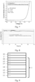
- Fig. 1 is a schematic representation of a vertical cross-section of a stack of layers 1 manufactured as part of embodiments of the present invention.
- the stack of layers 1 comprises a carrier substrate 11, which may function as the mechanical carrier of the optoelectronic device.
- the carrier substrate 11 may further function as a barrier against moisture and oxygen, and may be optically transparent.
- the carrier substrate 11 may be electrically insulating or electrically conductive.
- the stack of layers 1 comprises an electrically conductive bottom contact layer 12 on, i.e., in physical contact with, the substrate 11, for collecting holes from active layer 14, or for injecting holes into the active layer 14.
- the stack of layers 1 further comprises a p-type semiconducting layer 13 on, i.e., in physical contact with, the bottom contact layer 12.
- the p-type semiconducting layer 13 is for selectively transporting holes, and may form a barrier against movements of electrons.
- the stack of layers 1 further comprises an active layer 14 comprising an active material having a perovskite crystal structure.
- the active layer 14 is located on the p-type semiconducting layer 13.
- the physical contact between the p-type semiconducting layer 13 and the active layer 14 has the advantage that movement of electrons may be blocked at an interface of the p-type semiconducting 13 layer and the active layer 14. In other words, electrons may not be transported from the active layer 14 through a bottom surface of the active layer 14. Thereby, the electrons remain confined to the active layer 14 and to the layers over the active layer 14, which may, e.g., when considering a photovoltaic device, result in efficient collection of the electrons by a top contact.
- the stack of layers 1 further comprises an n-type semiconducting layer 15 comprising a fullerene, that is, in this example, located on the active layer 14.
- the physical contact between the n-type semiconducting layer 15 and the active layer 14 has the advantage that movement of holes may be blocked at an interface of the n-type semiconducting layer 15 and the active layer 14. In other words, holes may not be transported from the active layer 14 through a top surface of the active layer 14, and thereby remain confined to the active layer 14 and layers beneath the active layer 14, which may, e.g., when considering a photovoltaic device, result in good collection efficiency of the holes by the bottom contact layer 12.
- the stack of layers 1 further comprises an energy alignment layer 16 on, and in contact with, the n-type semiconducting layer 15.
- the energy alignment layer 16 comprises an exposed top surface 161.
- an n-type semiconducting metal oxide layer 2 is sputtered on the exposed top surface 161 of the energy alignment layer 16 of the stack of layers 1.
- the energy alignment layer 16 is in physical contact with both the n-type semiconducting layer 15 and the n-type semiconducting metal oxide layer 2.
- the energy alignment layer 16 provides good electrical contact, that is, good transport of electrons, between the n-type semiconducting layer 15 and the n-type semiconducting metal oxide layer 2.
- a top contact 3 is formed on the n-type semiconducting metal oxide layer 2.
- the top contact 3 is a layer, e.g., a metal or metal-oxide layer.
- a first inverted p-i-n photovoltaic cell was formed by using the stack design of Example 1, using a method in accordance with embodiments of the present invention.
- the substrate 11 consisted of glass.
- the bottom contact layer 12 was formed of indium tin oxide, and had a thickness of 120 nm.
- the bottom contact layer 12 was formed using magnetron sputtering.
- the p-type semiconducting layer 13 consisted of poly[bis(4-phenyl)(2,4,6-trimethylphenyl)amine (PTAA), and had a thickness of 5 nm.
- PTAA poly[bis(4-phenyl)(2,4,6-trimethylphenyl)amine
- the p-type semiconducting layer 13 was formed by spin coating.
- the active layer 14 consisted of a mixture of 95.23 mol-% Cs 0.1 FA 0.9 PbI 2.865 Br 0.135 and 4.76 mol-% FACl (wherein FA stands for formamidinium, i.e., [HC(NH 2 ) 2 ] + ).
- the active layer 14 was, in this example, spin coated and then annealed at 130 °C for 20 min in a N 2 atmosphere.
- the active layer 14 had a thickness of 500 nm.
- the n-type semiconducting layer 15 contained fullerene-C 60 and had a thickness of 40 nm.
- the n-type semiconducting layer 15 was formed by thermal evaporation at a rate of 1 ⁇ /s.
- the energy alignment layer 16 consisted of LiF, had a thickness of 0.8 nm, and was formed by thermal evaporation at a rate of 0.1 ⁇ /s.
- the n-type semiconducting metal oxide layer 2 consisted of ZnO and had a thickness of 15 nm.
- the n-type semiconducting metal oxide layer 2 was formed by magnetron sputtering under gentle conditions (low plasma power of 0.18 W/cm 2 , pressure of 3 Torr without extra substrate cooling or heating, namely soft sputtering).
- top contact 3 consisted of aluminium (i.e., is a metal layer), and had a thickness of 100 nm. The top contact 3 was formed by thermal evaporation at a rate of 2 ⁇ /s.
- a first reference photovoltaic cell was similar to the first inverted p-i-n photovoltaic cell, except that it did not contain the n-type semiconducting layer 15 nor the energy alignment layer 16. As such, the first reference photovoltaic cell only contained the n-type semiconducting metal oxide layer 2 on the active layer 14 and the top contact 3 on the n-type semiconducting metal oxide layer 2.
- a second reference photovoltaic cell was similar to the first inverted p-i-n photovoltaic cell, except that it did not contain the energy alignment layer 16. As such, the second reference photovoltaic cell contained the n-type semiconducting layer 15 on the active layer 14, the n-type semiconducting metal oxide layer 2 on n-type semiconducting layer 15, and the top contact 3 on the n-type semiconducting metal oxide layer 2.
- a third reference photovoltaic cell was similar to the first inverted p-i-n photovoltaic cell, except that it did not contain the n-type semiconducting layer 15. As such, the third reference photovoltaic cell contained the energy alignment layer 16 on the active layer 14, the n-type semiconducting metal oxide layer 2 on the energy alignment layer 16, and the top contact 3 on the n-type semiconducting metal oxide layer 2.
- Fig. 4 is a plot of current density-voltage (J-V) scanning curves, with current density plotted as a function of voltage, for the first inverted p-i-n photovoltaic cell (PV1; full curve), and for the first (Ref1; dotted curves with large spacing between adjacent dots), second (Ref2; dashed curve) and third reference photovoltaic cells (Ref3; dotted curves with small spacing between adjacent dots).
- a legend is included in Fig. 4 .
- Table 1 is an overview of figures of merit for the first inverted p-i-n photovoltaic cell (PV1), and for the first (Ref1), second (Ref2) and third (Ref3) reference photovoltaic cells.
- reverse refers to scans from an open circuit voltage (V oc ) to a short-circuit current density (J sc ), and forward refers to a scan from J sc to V oc .
- P in a standardized value of 1 kW/m 2 is used.
- Table 1 Experimental figures of merit for the perovskite cells with various photovoltaic cells. The hysteresis index is calculated as (PCE Reverse - PCE Forward )/PCE Reverse .
- the design of the second reference photovoltaic cell Ref2 resulted in an obvious S-shape barrier in the J-V curve.
- the energy alignment layer e.g., LiF layer
- the n-type semiconducting metal oxide layer is sputtered directly onto the active layer (corresponding to the first reference photovoltaic cell, Ref1)
- the photovoltaic cell also worked.
- the hysteresis between forward and reverse scans was considerable (see Table 1).
- the success rate of generating a working cell was rather low in this case (see below).
- the third reference Ref3 had an even worse hysteresis (Table 1), and the success rate was only slightly better than that of the second reference (see below).
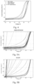
- Fig. 5A, 5B , 5C, and 5D show reverse J-V curves for a plurality photovoltaic cells fabricated with the design of PV1, Ref1, Ref2, and Ref3, respectively.
- the success rate that is the ratio of the number of working photovoltaic cells without shunting to the total number of working photovoltaic cells fabricated was rather low.
- the barrier in all the devices fabricated was removed, and a good success rate was achieved. Indeed, even though the energy alignment layer is thin (i.e., only 0.8 nm in this example) hence delicate, the mild conditions used for the sputtering did not negatively affect the quality of said energy alignment layer. Thereby, it appeared possible to take full advantage of the advantages of the energy alignment layer.
- the first inverted p-i-n photovoltaic cell was further compared with a typical inverted p-i-n photovoltaic cell of the state of the art, comprising, on the perovskite layer, a fullerene-C 60 layer, a bathocuproine layer on the fullerene-C 60 layer, and a top contact layer on the bathocuproine layer.
- Fig. 6 is a plot of a dark J-V curve for the first inverted p-i-n photovoltaic cell and for the typical inverted p-i-n photovoltaic cell of the state of the art.
- the first inverted p-i-n photovoltaic cell had a reduced dark current compared to the typical inverted p-i-n photovoltaic cell of the state of the. This strongly suggests that the energy alignment layer is not negatively affected by the sputtering process of the present invention.
- a second inverted p-i-n photovoltaic cell was formed in accordance with the stack design of Example 1, using a method in accordance with embodiments of the present invention.
- the second inverted p-i-n photovoltaic cell is formed with the same features as the first inverted p-i-n photovoltaic cell, except that a different active layer and a different top contact are formed.
- the active layer of the second inverted p-i-n photovoltaic cell contained 76.9 mol-% Cs 0.1 FA 0.9 Pb(I 0.9 Br 0.1 ) 3 (wherein FA stands for formamidinium, i.e., [HC(NH 2 ) 2 ] + ) and 23.1 mol-% MACl (where MA stands for methylammonium, i.e., [CH 3 NH 3 ] + ).
- the active layer was also in this example deposited using spin coating, but annealed at 110°C for 40 min in a N 2 atmosphere.
- the top contact of the second inverted p-i-n photovoltaic cell consisted of silver.
- Fig. 7 is a plot of a J-V scan for the second inverted p-i-n photovoltaic cell. No S-shaped barrier is observed in the J-V scan.
- PCE normalized power conversion efficiency
- the method of the present invention also results in a good photovoltaic cell for this alternative composition of the active layer.
- this example confirms that the conditions for the sputtering are such that the energy alignment layer is not damaged, so that its positive effect on the electronic and structural properties is still clear. This is also indicated by the limited degradation illustrated in Fig. 8 .
- Example 2 Forming of an optoelectronic device comprising a further energy alignment layer
- Fig. 9 is an example of an optoelectronic device in accordance with embodiments of the present invention, comprising a further energy alignment layer 17.
- the part of the stack of layers 1 consisting of the carrier substrate 11, the bottom contact layer 12, the p-type semiconducting layer 13, and the active layer 14 has, in this example, identical features and advantages as the corresponding layers of Example 1.
- the further energy alignment layer 17 is formed on the active layer 14.
- the n-type semiconducting layer 15 is formed on the further energy alignment layer 17.
- the function of the further energy alignment layer 17 is to improve electrical contact between the active layer 14 and the n-type semiconducting layer 15.
- the n-type semiconducting layer 15, the energy alignment layer 16, the n-type semiconducting metal oxide layer 2, and the top contact, i.e., metal layer 32 have the same features and advantages as the corresponding layers of Example 1.
- a third inverted p-i-n photovoltaic cell was formed, in the same way as the second inverted p-i-n photovoltaic cell, except that the further energy alignment layer 17 was included as indicated above.
- the further energy alignment layer 17 consisted of LiF, had a thickness of 0.8 nm, and was formed by thermal evaporation at a rate of 0.1 ⁇ /s.
- Fig. 10 is a plot of a J-V curve for the third inverted p-i-n photovoltaic cell in forward and reverse scan mode.
- Fig. 11 is a plot of the PCE at maximum power point condition as a function of time, under 1-sun equivalent illumination (corresponding to 1000 W/m 2 ) and 30°C and in a N 2 atmosphere, indicating good stability for the third inverted p-i-n photovoltaic cell.
- Comparison with the first inverted p-i-n photovoltaic cell shows an improved PCE and hysteresis index for the third inverted p-i-n photovoltaic cell, indicating the positive effect of the further energy alignment layer.
- Example 3 Further optoelectronic devices
- Fig. 12 is a schematic representation of an optoelectronic device manufactured in accordance with embodiments of the present invention.
- the optoelectronic device is arranged for at least receiving light through a top surface thereof.
- the substrate 11 may be glass sheet or transparent plastic based substrate for semi-transparent devices.
- the substrate 11 may be a non-transparent substrate, such as a metal foil.
- Layers 12 to 16 and the n-type semiconducting metal oxide layer 2, that is preferably optically transparent, may be the same, and formed in the same way, as the corresponding layers of Example 1. However, in this example, the top contact that is formed is different.
- the top contact comprises an optically transparent, electrically conductive metal oxide layer 30, formed on the n-type semiconducting metal oxide layer 2.
- the conductive metal oxide layer 30 may act as a lateral charge collecting electrode.
- the top contact comprises a further metal grid 4, formed on the conductive metal oxide layer 30.
- the further metal grid 4 preferably has a small width.
- a top surface 31 of the optically transparent, electrically conductive metal oxide layer 30 comprises a first region covered by the further metal grid 4, and a second region not covered by the further metal grid 4, e.g., exposed to air or covered by a non-conducting, optically transparent polymer material.
- a ratio of an area of the second region to an area of the first region is as large as possible, e.g., at least 10.
- Fig. 13 is a schematic representation of an optoelectronic device manufactured in accordance with embodiments of the present invention.
- This example is the same as that of Fig. 12 , except that in this example, there is no optically transparent, electrically conductive metal oxide layer 30, formed on the n-type semiconducting metal oxide layer 2.
- This example comprises a metal grid 4 on top of the n-type semiconducting metal oxide layer 2.
- the n-type semiconducting metal oxide layer 2 is, in this example, optically transparent and electrically conductive, serving both as electron transport layer and as top transparent conductive oxide.
- indium tin oxide may be a suitable material for the n-type semiconducting metal oxide layer 2.
- Fig. 14 is a schematic representation of an optoelectronic device manufactured in accordance with embodiments of the present invention.
- the optoelectronic device of this example is similar as that of Example 2, except that the top contact is not a metal layer, but a further metal grid 4 formed on an optically transparent, electrically conductive metal oxide layer 30. This configuration may facilitate light transmission through the layers above the active layer 14.
- Fig. 15 This example is similar as that described above in relation to Fig. 12 , except that no additional bottom contact layer 12 is present in addition to the carrier substrate 11, that is in this example a metal sheet or foil.
- the carrier substrate 11 is the bottom contact layer 12.
- the carrier substrate 11 acts as bottom contact, i.e., as anode electrode. Potential metal diffusion from the carrier substrate may be prevented by the p-type semiconducting layer 13.
- Fig. 16 This example is similar as that described above in relation to Fig. 15 , except that this example does not comprise the optically transparent, electrically conductive metal oxide layer 30.
- a metal grid 4 is deposited directly on top of the n-type semiconducting metal oxide layer 2.
- Fig. 17 This example is similar as that described above in relation to Fig. 15 , except for the further energy alignment layer 17 that is in this example located between the active layer 14 and the n-type semiconducting layer 15.
- Fig. 18 This example is similar as that described above in relation to Fig. 16 , except for the further energy alignment layer 17 that is in this example located between the active layer 14 and the n-type semiconducting layer 15.
Landscapes
- Engineering & Computer Science (AREA)
- Chemical & Material Sciences (AREA)
- Power Engineering (AREA)
- Physics & Mathematics (AREA)
- Electromagnetism (AREA)
- Materials Engineering (AREA)
- Chemical Kinetics & Catalysis (AREA)
- Electrochemistry (AREA)
- Manufacturing & Machinery (AREA)
- Microelectronics & Electronic Packaging (AREA)
- Photovoltaic Devices (AREA)
Claims (15)
- Ein Verfahren zum Bilden einer Zwischenstruktur bei der Bildung einer optoelektronischen Vorrichtung, wobei das Verfahren umfasst:a)- Erhalten eines Schichtenstapels (1) über einem Substrathalter in einer Sputterkammer, wobei der Schichtenstapel (1) umfasst:eine aktive Schicht (14), die ein aktives Material umfasst, das eine Perowskit-Kristallstruktur aufweist,eine n-Typ-Halbleiterschicht (15), die ein Fulleren umfasst, über der aktiven Schicht (14), undeine Energieausrichtungsschicht (16), die ein Lithiumhalogenid, ein Magnesiumhalogenid, Al2O3 oder ein Metallfluorid auf und in Kontakt mit der n-Typ-Halbleiterschicht (15) umfasst, wobei die Energieausrichtungsschicht (16) eine freiliegende obere Fläche (161) umfasst, undb)- Sputtern einer n-Typ-Halbleiter-Metalloxidschicht (2) auf die freiliegende obere Fläche (161) der Energieausrichtungsschicht (16), wobei das Sputtern mit einer Sputterleistungsdichte von höchstens 1 W·cm-2 und bei einer Temperatur des Schichtenstapels von höchstens 100 °C durchgeführt wird.
- Das Verfahren nach Anspruch 1, das weiter nach Schritt b einen Schritt c zum Bilden eines oberen Kontakts (3) über der Metalloxidschicht (2) umfasst, wobei der obere Kontakt (3) eine Metallschicht (32), ein Metallgitter (4) und/oder eine optisch transparente, elektrisch leitfähige Metalloxidschicht (30) umfasst.
- Das Verfahren nach Anspruch 1 oder Anspruch 2, wobei das Sputtern unter aktiver Kühlung des Schichtenstapels (1) durchgeführt wird.
- Das Verfahren nach einem der vorstehenden Ansprüche, wobei das Sputtern bei einem Druck von 0,1 Pa bis 7 Pa durchgeführt wird.
- Das Verfahren nach Anspruch 4, wobei das Sputtern bei einem Druck von 0,2 Pa bis 0,7 Pa durchgeführt wird.
- Das Verfahren nach einem der vorstehenden Ansprüche, wobei das Sputtern mit einem Abstand zwischen einem für das Sputtern verwendeten Target und einer oberen Fläche des Schichtenstapels (1) von 5 cm bis 50 cm durchgeführt wird.
- Das Verfahren nach einem der vorstehenden Ansprüche, wobei das Erhalten des Schichtenstapels (1) das Erhalten des Schichtenstapels umfasst, wobei die Energieausrichtungsschicht (16) eine Dicke von 0,5 nm bis 2 nm aufweist.
- Das Verfahren nach einem der vorstehenden Ansprüche, wobei das Erhalten des Schichtenstapels (1) das Erhalten eines unteren Kontaktierungsstapels umfasst, wobei sich die aktive Schicht (14) über dem unteren Kontaktierungsstapel befindet, wobei der untere Kontaktierungsstapel umfasst:eine untere Kontaktschicht (12), die eine Metallschicht und/oder eine optisch transparente, elektrisch leitfähige Metalloxidschicht umfasst, undeine p-Typ-Halbleiterschicht (13) über der unteren Kontaktschicht (12).
- Das Verfahren nach Anspruch 8, wobei der untere Kontaktierungsstapel weiter ein elektrisch isolierendes, optisch transparentes Substrat (11) umfasst, wobei sich die untere Kontaktschicht (12) über dem optisch transparenten Substrat (11) befindet, und wobei die untere Kontaktschicht (12) optisch transparent ist.
- Das Verfahren nach einem der vorstehenden Ansprüche, wobei das Erhalten des Schichtenstapels (1) weiter das Erhalten einer weiteren Energieausrichtungsschicht (17) umfasst, die ein Lithiumhalogenid, ein Magnesiumfluorid oder ein Metallfluorid umfasst, die sich zwischen der aktiven Schicht (14) und der n-Typ-Halbleiterschicht (15) befindet und diese kontaktiert.
- Das Verfahren nach einem der vorstehenden Ansprüche, wobei die gesputterte Metalloxidschicht (2) eine Dicke von 10 nm bis 1000 nm aufweist.
- Das Verfahren nach einem der vorstehenden Ansprüche, wobei die gesputterte Metalloxidschicht (2) eines der Folgenden umfasst: Zinkoxid, Zinnoxid, Titanoxid, oder ein transparentes, leitfähiges Metalloxid, das Indiumoxid umfasst.
- Das Verfahren nach einem der vorstehenden Ansprüche, wobei die Energieausrichtungsschicht (16) Lithiumfluorid oder Magnesiumfluorid umfasst.
- Das Verfahren nach einem der vorstehenden Ansprüche, wobei die n-Typ-Halbleiterschicht (15) [6,6]-Phenyl-C61-buttersäuremethylester oder Fulleren-C60 umfasst.
- Das Verfahren nach einem der vorstehenden Ansprüche, wobei die n-Typ-Halbleiterschicht (15) eine Dicke von 10 nm bis 50 nm aufweist.
Priority Applications (3)
| Application Number | Priority Date | Filing Date | Title |
|---|---|---|---|
| ES21215793T ES2991273T3 (es) | 2021-12-19 | 2021-12-19 | Formación de dispositivos optoelectrónicos basados en perovskita |
| EP21215793.7A EP4199126B1 (de) | 2021-12-19 | 2021-12-19 | Herstellung von perowskitbasierten optoelektronischen vorrichtungen |
| US18/064,075 US12334276B2 (en) | 2021-12-19 | 2022-12-09 | Method for forming of perovskite-based optoelectronic devices |
Applications Claiming Priority (1)
| Application Number | Priority Date | Filing Date | Title |
|---|---|---|---|
| EP21215793.7A EP4199126B1 (de) | 2021-12-19 | 2021-12-19 | Herstellung von perowskitbasierten optoelektronischen vorrichtungen |
Publications (2)
| Publication Number | Publication Date |
|---|---|
| EP4199126A1 EP4199126A1 (de) | 2023-06-21 |
| EP4199126B1 true EP4199126B1 (de) | 2024-07-31 |
Family
ID=79018710
Family Applications (1)
| Application Number | Title | Priority Date | Filing Date |
|---|---|---|---|
| EP21215793.7A Active EP4199126B1 (de) | 2021-12-19 | 2021-12-19 | Herstellung von perowskitbasierten optoelektronischen vorrichtungen |
Country Status (3)
| Country | Link |
|---|---|
| US (1) | US12334276B2 (de) |
| EP (1) | EP4199126B1 (de) |
| ES (1) | ES2991273T3 (de) |
Families Citing this family (1)
| Publication number | Priority date | Publication date | Assignee | Title |
|---|---|---|---|---|
| AT18402U1 (de) * | 2023-09-20 | 2025-02-15 | Ev Group E Thallner Gmbh | Verfahren und Vorrichtung zur Erzeugung von großflächigen dünnen Schichten an Substraten mittels chemisch reaktiver Sprühbeschichtung |
Family Cites Families (2)
| Publication number | Priority date | Publication date | Assignee | Title |
|---|---|---|---|---|
| GB201820427D0 (en) * | 2018-12-14 | 2019-01-30 | Univ Oxford Innovation Ltd | Device interlayer |
| GB2583965A (en) * | 2019-05-16 | 2020-11-18 | Oxford Photovoltaics Ltd | Photovoltaic device |
-
2021
- 2021-12-19 ES ES21215793T patent/ES2991273T3/es active Active
- 2021-12-19 EP EP21215793.7A patent/EP4199126B1/de active Active
-
2022
- 2022-12-09 US US18/064,075 patent/US12334276B2/en active Active
Also Published As
| Publication number | Publication date |
|---|---|
| US12334276B2 (en) | 2025-06-17 |
| EP4199126A1 (de) | 2023-06-21 |
| US20230197353A1 (en) | 2023-06-22 |
| ES2991273T3 (es) | 2024-12-03 |
Similar Documents
| Publication | Publication Date | Title |
|---|---|---|
| US11158828B2 (en) | Solar cell comprising an oxide-nanoparticle buffer layer and method of fabrication | |
| KR102756417B1 (ko) | 텐덤 태양전지 | |
| EP2313926B1 (de) | Verfahren zur herstellung von photovoltaischen modulen | |
| KR101560640B1 (ko) | 광을 수집할 수 있는 요소의 개선 | |
| US20120037225A1 (en) | Solar cell and method of fabricating the same | |
| US20090090618A1 (en) | Solar cell and method for manufacturing the same | |
| US20150040962A1 (en) | Solar Cell and Method of Fabricating the Same | |
| WO2009136863A1 (en) | An electrically conducting structure for a light transmissible device | |
| Reddy et al. | Holistic approach toward a damage-less sputtered indium tin oxide barrier layer for high-stability inverted perovskite solar cells and modules | |
| US11205735B2 (en) | Low temperature p-i-n hybrid mesoporous optoelectronic device | |
| US12334276B2 (en) | Method for forming of perovskite-based optoelectronic devices | |
| EP4325586A1 (de) | Solarbatterie | |
| WO2022071302A1 (ja) | ペロブスカイト薄膜系太陽電池の製造方法 | |
| CN116322222A (zh) | 一种钙钛矿/晶硅叠层太阳能电池组件及其制备方法 | |
| CN119866129A (zh) | 一种钙钛矿太阳能电池及其制备方法 | |
| Chakaroun et al. | ITO/Au/ITO multilayer electrodes for CuPc/C60 solar cells | |
| US20250393340A1 (en) | Solar cell and method for preparing same, photovoltaic module and power consuming device | |
| EP4538232A1 (de) | Perowskitverbindung und fotoelektrisches umwandlungselement | |
| US20140373916A1 (en) | Photovoltaic device and method of manufacture | |
| US20240204122A1 (en) | Thin-film solar cell capable of independently adjusting transparency and color and method of manufacturing the same | |
| KR20170052398A (ko) | 투명 전극, 투명 전극의 제조 방법 및 이를 포함하는 유기 광전자 소자 | |
| KR20250077034A (ko) | 양면수광형 박막태양전지 및 그 제조방법 | |
| JP2004335136A (ja) | 有機発光素子 | |
| KR101928584B1 (ko) | 형광체를 포함하는 태양전지 및 이의 제조방법 | |
| KR20170121101A (ko) | 투명 전극, 투명 전극의 제조 방법 및 이를 포함하는 유기 광전자 소자 |
Legal Events
| Date | Code | Title | Description |
|---|---|---|---|
| PUAI | Public reference made under article 153(3) epc to a published international application that has entered the european phase |
Free format text: ORIGINAL CODE: 0009012 |
|
| STAA | Information on the status of an ep patent application or granted ep patent |
Free format text: STATUS: THE APPLICATION HAS BEEN PUBLISHED |
|
| AK | Designated contracting states |
Kind code of ref document: A1 Designated state(s): AL AT BE BG CH CY CZ DE DK EE ES FI FR GB GR HR HU IE IS IT LI LT LU LV MC MK MT NL NO PL PT RO RS SE SI SK SM TR |
|
| STAA | Information on the status of an ep patent application or granted ep patent |
Free format text: STATUS: REQUEST FOR EXAMINATION WAS MADE |
|
| 17P | Request for examination filed |
Effective date: 20231030 |
|
| RBV | Designated contracting states (corrected) |
Designated state(s): AL AT BE BG CH CY CZ DE DK EE ES FI FR GB GR HR HU IE IS IT LI LT LU LV MC MK MT NL NO PL PT RO RS SE SI SK SM TR |
|
| REG | Reference to a national code |
Ref country code: DE Ref legal event code: R079 Free format text: PREVIOUS MAIN CLASS: H01L0051000000 Ipc: H10K0030200000 Ref document number: 602021016441 Country of ref document: DE |
|
| GRAP | Despatch of communication of intention to grant a patent |
Free format text: ORIGINAL CODE: EPIDOSNIGR1 |
|
| STAA | Information on the status of an ep patent application or granted ep patent |
Free format text: STATUS: GRANT OF PATENT IS INTENDED |
|
| RIC1 | Information provided on ipc code assigned before grant |
Ipc: H10K 85/20 20230101ALN20240215BHEP Ipc: H10K 30/50 20230101ALN20240215BHEP Ipc: H10K 85/50 20230101ALI20240215BHEP Ipc: H10K 71/16 20230101ALI20240215BHEP Ipc: H10K 30/40 20230101ALI20240215BHEP Ipc: H10K 30/20 20230101AFI20240215BHEP |
|
| INTG | Intention to grant announced |
Effective date: 20240301 |
|
| RIC1 | Information provided on ipc code assigned before grant |
Ipc: H10K 85/20 20230101ALN20240220BHEP Ipc: H10K 30/50 20230101ALN20240220BHEP Ipc: H10K 85/50 20230101ALI20240220BHEP Ipc: H10K 71/16 20230101ALI20240220BHEP Ipc: H10K 30/40 20230101ALI20240220BHEP Ipc: H10K 30/20 20230101AFI20240220BHEP |
|
| P01 | Opt-out of the competence of the unified patent court (upc) registered |
Effective date: 20240328 |
|
| GRAS | Grant fee paid |
Free format text: ORIGINAL CODE: EPIDOSNIGR3 |
|
| GRAA | (expected) grant |
Free format text: ORIGINAL CODE: 0009210 |
|
| STAA | Information on the status of an ep patent application or granted ep patent |
Free format text: STATUS: THE PATENT HAS BEEN GRANTED |
|
| AK | Designated contracting states |
Kind code of ref document: B1 Designated state(s): AL AT BE BG CH CY CZ DE DK EE ES FI FR GB GR HR HU IE IS IT LI LT LU LV MC MK MT NL NO PL PT RO RS SE SI SK SM TR |
|
| REG | Reference to a national code |
Ref country code: CH Ref legal event code: EP Ref country code: GB Ref legal event code: FG4D |
|
| REG | Reference to a national code |
Ref country code: DE Ref legal event code: R096 Ref document number: 602021016441 Country of ref document: DE |
|
| REG | Reference to a national code |
Ref country code: IE Ref legal event code: FG4D |
|
| REG | Reference to a national code |
Ref country code: LT Ref legal event code: MG9D |
|
| REG | Reference to a national code |
Ref country code: ES Ref legal event code: FG2A Ref document number: 2991273 Country of ref document: ES Kind code of ref document: T3 Effective date: 20241203 |
|
| REG | Reference to a national code |
Ref country code: NL Ref legal event code: MP Effective date: 20240731 |
|
| PG25 | Lapsed in a contracting state [announced via postgrant information from national office to epo] |
Ref country code: PT Free format text: LAPSE BECAUSE OF FAILURE TO SUBMIT A TRANSLATION OF THE DESCRIPTION OR TO PAY THE FEE WITHIN THE PRESCRIBED TIME-LIMIT Effective date: 20241202 |
|
| REG | Reference to a national code |
Ref country code: AT Ref legal event code: MK05 Ref document number: 1709822 Country of ref document: AT Kind code of ref document: T Effective date: 20240731 |
|
| PG25 | Lapsed in a contracting state [announced via postgrant information from national office to epo] |
Ref country code: PT Free format text: LAPSE BECAUSE OF FAILURE TO SUBMIT A TRANSLATION OF THE DESCRIPTION OR TO PAY THE FEE WITHIN THE PRESCRIBED TIME-LIMIT Effective date: 20241202 |
|
| PG25 | Lapsed in a contracting state [announced via postgrant information from national office to epo] |
Ref country code: NO Free format text: LAPSE BECAUSE OF FAILURE TO SUBMIT A TRANSLATION OF THE DESCRIPTION OR TO PAY THE FEE WITHIN THE PRESCRIBED TIME-LIMIT Effective date: 20241031 |
|
| PG25 | Lapsed in a contracting state [announced via postgrant information from national office to epo] |
Ref country code: GR Free format text: LAPSE BECAUSE OF FAILURE TO SUBMIT A TRANSLATION OF THE DESCRIPTION OR TO PAY THE FEE WITHIN THE PRESCRIBED TIME-LIMIT Effective date: 20241101 Ref country code: NL Free format text: LAPSE BECAUSE OF FAILURE TO SUBMIT A TRANSLATION OF THE DESCRIPTION OR TO PAY THE FEE WITHIN THE PRESCRIBED TIME-LIMIT Effective date: 20240731 Ref country code: PL Free format text: LAPSE BECAUSE OF FAILURE TO SUBMIT A TRANSLATION OF THE DESCRIPTION OR TO PAY THE FEE WITHIN THE PRESCRIBED TIME-LIMIT Effective date: 20240731 Ref country code: FI Free format text: LAPSE BECAUSE OF FAILURE TO SUBMIT A TRANSLATION OF THE DESCRIPTION OR TO PAY THE FEE WITHIN THE PRESCRIBED TIME-LIMIT Effective date: 20240731 |
|
| PG25 | Lapsed in a contracting state [announced via postgrant information from national office to epo] |
Ref country code: BG Free format text: LAPSE BECAUSE OF FAILURE TO SUBMIT A TRANSLATION OF THE DESCRIPTION OR TO PAY THE FEE WITHIN THE PRESCRIBED TIME-LIMIT Effective date: 20240731 |
|
| PG25 | Lapsed in a contracting state [announced via postgrant information from national office to epo] |
Ref country code: LV Free format text: LAPSE BECAUSE OF FAILURE TO SUBMIT A TRANSLATION OF THE DESCRIPTION OR TO PAY THE FEE WITHIN THE PRESCRIBED TIME-LIMIT Effective date: 20240731 |
|
| PG25 | Lapsed in a contracting state [announced via postgrant information from national office to epo] |
Ref country code: IS Free format text: LAPSE BECAUSE OF FAILURE TO SUBMIT A TRANSLATION OF THE DESCRIPTION OR TO PAY THE FEE WITHIN THE PRESCRIBED TIME-LIMIT Effective date: 20241130 Ref country code: AT Free format text: LAPSE BECAUSE OF FAILURE TO SUBMIT A TRANSLATION OF THE DESCRIPTION OR TO PAY THE FEE WITHIN THE PRESCRIBED TIME-LIMIT Effective date: 20240731 |
|
| PG25 | Lapsed in a contracting state [announced via postgrant information from national office to epo] |
Ref country code: HR Free format text: LAPSE BECAUSE OF FAILURE TO SUBMIT A TRANSLATION OF THE DESCRIPTION OR TO PAY THE FEE WITHIN THE PRESCRIBED TIME-LIMIT Effective date: 20240731 |
|
| PG25 | Lapsed in a contracting state [announced via postgrant information from national office to epo] |
Ref country code: RS Free format text: LAPSE BECAUSE OF FAILURE TO SUBMIT A TRANSLATION OF THE DESCRIPTION OR TO PAY THE FEE WITHIN THE PRESCRIBED TIME-LIMIT Effective date: 20241031 |
|
| PG25 | Lapsed in a contracting state [announced via postgrant information from national office to epo] |
Ref country code: RS Free format text: LAPSE BECAUSE OF FAILURE TO SUBMIT A TRANSLATION OF THE DESCRIPTION OR TO PAY THE FEE WITHIN THE PRESCRIBED TIME-LIMIT Effective date: 20241031 Ref country code: PL Free format text: LAPSE BECAUSE OF FAILURE TO SUBMIT A TRANSLATION OF THE DESCRIPTION OR TO PAY THE FEE WITHIN THE PRESCRIBED TIME-LIMIT Effective date: 20240731 Ref country code: NO Free format text: LAPSE BECAUSE OF FAILURE TO SUBMIT A TRANSLATION OF THE DESCRIPTION OR TO PAY THE FEE WITHIN THE PRESCRIBED TIME-LIMIT Effective date: 20241031 Ref country code: NL Free format text: LAPSE BECAUSE OF FAILURE TO SUBMIT A TRANSLATION OF THE DESCRIPTION OR TO PAY THE FEE WITHIN THE PRESCRIBED TIME-LIMIT Effective date: 20240731 Ref country code: LV Free format text: LAPSE BECAUSE OF FAILURE TO SUBMIT A TRANSLATION OF THE DESCRIPTION OR TO PAY THE FEE WITHIN THE PRESCRIBED TIME-LIMIT Effective date: 20240731 Ref country code: IS Free format text: LAPSE BECAUSE OF FAILURE TO SUBMIT A TRANSLATION OF THE DESCRIPTION OR TO PAY THE FEE WITHIN THE PRESCRIBED TIME-LIMIT Effective date: 20241130 Ref country code: HR Free format text: LAPSE BECAUSE OF FAILURE TO SUBMIT A TRANSLATION OF THE DESCRIPTION OR TO PAY THE FEE WITHIN THE PRESCRIBED TIME-LIMIT Effective date: 20240731 Ref country code: GR Free format text: LAPSE BECAUSE OF FAILURE TO SUBMIT A TRANSLATION OF THE DESCRIPTION OR TO PAY THE FEE WITHIN THE PRESCRIBED TIME-LIMIT Effective date: 20241101 Ref country code: FI Free format text: LAPSE BECAUSE OF FAILURE TO SUBMIT A TRANSLATION OF THE DESCRIPTION OR TO PAY THE FEE WITHIN THE PRESCRIBED TIME-LIMIT Effective date: 20240731 Ref country code: BG Free format text: LAPSE BECAUSE OF FAILURE TO SUBMIT A TRANSLATION OF THE DESCRIPTION OR TO PAY THE FEE WITHIN THE PRESCRIBED TIME-LIMIT Effective date: 20240731 Ref country code: AT Free format text: LAPSE BECAUSE OF FAILURE TO SUBMIT A TRANSLATION OF THE DESCRIPTION OR TO PAY THE FEE WITHIN THE PRESCRIBED TIME-LIMIT Effective date: 20240731 |
|
| PG25 | Lapsed in a contracting state [announced via postgrant information from national office to epo] |
Ref country code: RO Free format text: LAPSE BECAUSE OF FAILURE TO SUBMIT A TRANSLATION OF THE DESCRIPTION OR TO PAY THE FEE WITHIN THE PRESCRIBED TIME-LIMIT Effective date: 20240731 Ref country code: DK Free format text: LAPSE BECAUSE OF FAILURE TO SUBMIT A TRANSLATION OF THE DESCRIPTION OR TO PAY THE FEE WITHIN THE PRESCRIBED TIME-LIMIT Effective date: 20240731 Ref country code: SM Free format text: LAPSE BECAUSE OF FAILURE TO SUBMIT A TRANSLATION OF THE DESCRIPTION OR TO PAY THE FEE WITHIN THE PRESCRIBED TIME-LIMIT Effective date: 20240731 |
|
| PG25 | Lapsed in a contracting state [announced via postgrant information from national office to epo] |
Ref country code: EE Free format text: LAPSE BECAUSE OF FAILURE TO SUBMIT A TRANSLATION OF THE DESCRIPTION OR TO PAY THE FEE WITHIN THE PRESCRIBED TIME-LIMIT Effective date: 20240731 |
|
| PG25 | Lapsed in a contracting state [announced via postgrant information from national office to epo] |
Ref country code: CZ Free format text: LAPSE BECAUSE OF FAILURE TO SUBMIT A TRANSLATION OF THE DESCRIPTION OR TO PAY THE FEE WITHIN THE PRESCRIBED TIME-LIMIT Effective date: 20240731 |
|
| PG25 | Lapsed in a contracting state [announced via postgrant information from national office to epo] |
Ref country code: IT Free format text: LAPSE BECAUSE OF FAILURE TO SUBMIT A TRANSLATION OF THE DESCRIPTION OR TO PAY THE FEE WITHIN THE PRESCRIBED TIME-LIMIT Effective date: 20240731 Ref country code: SK Free format text: LAPSE BECAUSE OF FAILURE TO SUBMIT A TRANSLATION OF THE DESCRIPTION OR TO PAY THE FEE WITHIN THE PRESCRIBED TIME-LIMIT Effective date: 20240731 |
|
| REG | Reference to a national code |
Ref country code: DE Ref legal event code: R097 Ref document number: 602021016441 Country of ref document: DE |
|
| PLBE | No opposition filed within time limit |
Free format text: ORIGINAL CODE: 0009261 |
|
| STAA | Information on the status of an ep patent application or granted ep patent |
Free format text: STATUS: NO OPPOSITION FILED WITHIN TIME LIMIT |
|
| PG25 | Lapsed in a contracting state [announced via postgrant information from national office to epo] |
Ref country code: MC Free format text: LAPSE BECAUSE OF FAILURE TO SUBMIT A TRANSLATION OF THE DESCRIPTION OR TO PAY THE FEE WITHIN THE PRESCRIBED TIME-LIMIT Effective date: 20240731 |
|
| 26N | No opposition filed |
Effective date: 20250501 |
|
| REG | Reference to a national code |
Ref country code: CH Ref legal event code: PL |
|
| PG25 | Lapsed in a contracting state [announced via postgrant information from national office to epo] |
Ref country code: LU Free format text: LAPSE BECAUSE OF NON-PAYMENT OF DUE FEES Effective date: 20241219 |
|
| PG25 | Lapsed in a contracting state [announced via postgrant information from national office to epo] |
Ref country code: SE Free format text: LAPSE BECAUSE OF FAILURE TO SUBMIT A TRANSLATION OF THE DESCRIPTION OR TO PAY THE FEE WITHIN THE PRESCRIBED TIME-LIMIT Effective date: 20240731 |
|
| REG | Reference to a national code |
Ref country code: BE Ref legal event code: MM Effective date: 20241231 |
|
| PG25 | Lapsed in a contracting state [announced via postgrant information from national office to epo] |
Ref country code: BE Free format text: LAPSE BECAUSE OF NON-PAYMENT OF DUE FEES Effective date: 20241231 |
|
| PG25 | Lapsed in a contracting state [announced via postgrant information from national office to epo] |
Ref country code: FR Free format text: LAPSE BECAUSE OF NON-PAYMENT OF DUE FEES Effective date: 20241231 |
|
| PG25 | Lapsed in a contracting state [announced via postgrant information from national office to epo] |
Ref country code: CH Free format text: LAPSE BECAUSE OF NON-PAYMENT OF DUE FEES Effective date: 20241231 |
|
| PG25 | Lapsed in a contracting state [announced via postgrant information from national office to epo] |
Ref country code: IE Free format text: LAPSE BECAUSE OF NON-PAYMENT OF DUE FEES Effective date: 20241219 |
|
| PGFP | Annual fee paid to national office [announced via postgrant information from national office to epo] |
Ref country code: DE Payment date: 20251126 Year of fee payment: 5 |
|
| PGFP | Annual fee paid to national office [announced via postgrant information from national office to epo] |
Ref country code: ES Payment date: 20260102 Year of fee payment: 5 |
|
| PG25 | Lapsed in a contracting state [announced via postgrant information from national office to epo] |
Ref country code: CY Free format text: LAPSE BECAUSE OF FAILURE TO SUBMIT A TRANSLATION OF THE DESCRIPTION OR TO PAY THE FEE WITHIN THE PRESCRIBED TIME-LIMIT Effective date: 20240731 |