EP4196331B1 - Porteur de composant électrique - Google Patents
Porteur de composant électrique Download PDFInfo
- Publication number
- EP4196331B1 EP4196331B1 EP21762018.6A EP21762018A EP4196331B1 EP 4196331 B1 EP4196331 B1 EP 4196331B1 EP 21762018 A EP21762018 A EP 21762018A EP 4196331 B1 EP4196331 B1 EP 4196331B1
- Authority
- EP
- European Patent Office
- Prior art keywords
- carrier element
- electronic component
- filling material
- gas bubbles
- contact surface
- Prior art date
- Legal status (The legal status is an assumption and is not a legal conclusion. Google has not performed a legal analysis and makes no representation as to the accuracy of the status listed.)
- Active
Links
Images
Classifications
-
- B—PERFORMING OPERATIONS; TRANSPORTING
- B29—WORKING OF PLASTICS; WORKING OF SUBSTANCES IN A PLASTIC STATE IN GENERAL
- B29C—SHAPING OR JOINING OF PLASTICS; SHAPING OF MATERIAL IN A PLASTIC STATE, NOT OTHERWISE PROVIDED FOR; AFTER-TREATMENT OF THE SHAPED PRODUCTS, e.g. REPAIRING
- B29C45/00—Injection moulding, i.e. forcing the required volume of moulding material through a nozzle into a closed mould; Apparatus therefor
- B29C45/0005—Injection moulding, i.e. forcing the required volume of moulding material through a nozzle into a closed mould; Apparatus therefor using fibre reinforcements
-
- B—PERFORMING OPERATIONS; TRANSPORTING
- B29—WORKING OF PLASTICS; WORKING OF SUBSTANCES IN A PLASTIC STATE IN GENERAL
- B29C—SHAPING OR JOINING OF PLASTICS; SHAPING OF MATERIAL IN A PLASTIC STATE, NOT OTHERWISE PROVIDED FOR; AFTER-TREATMENT OF THE SHAPED PRODUCTS, e.g. REPAIRING
- B29C45/00—Injection moulding, i.e. forcing the required volume of moulding material through a nozzle into a closed mould; Apparatus therefor
- B29C45/17—Component parts, details or accessories; Auxiliary operations
- B29C45/1703—Introducing an auxiliary fluid into the mould
- B29C45/1704—Introducing an auxiliary fluid into the mould the fluid being introduced into the interior of the injected material which is still in a molten state, e.g. for producing hollow articles
-
- B—PERFORMING OPERATIONS; TRANSPORTING
- B29—WORKING OF PLASTICS; WORKING OF SUBSTANCES IN A PLASTIC STATE IN GENERAL
- B29L—INDEXING SCHEME ASSOCIATED WITH SUBCLASS B29C, RELATING TO PARTICULAR ARTICLES
- B29L2031/00—Other particular articles
- B29L2031/34—Electrical apparatus, e.g. sparking plugs or parts thereof
- B29L2031/3481—Housings or casings incorporating or embedding electric or electronic elements
Definitions
- the present invention relates to a device for enclosing an electronic component in a moisture-tight manner. A method for producing the device is also described.
- a device for moisture-tight housing of an electronic component and its conductor has a fiber-reinforced, injection-molded carrier element which has a cavity for receiving the electronic component and consists of a thermoplastic.
- the device also has the electronic component which is arranged in the cavity.
- the device also has a filling compound which adheres to the carrier element and the electronic component and is arranged between the electronic component and the carrier element.
- the device also has an electrical conductor which is coupled to the electronic component and the carrier element and is at least partially surrounded by the filling compound.
- the carrier element contains gas bubbles which are less than 10 mm away from the filling compound.
- a method for producing a device described above for enclosing a conductor of an electronic component in a moisture-tight manner comprises injection molding of a fiber-reinforced carrier element which has a cavity for receiving the electronic component and is made of a thermoplastic material.
- the electronic Component is arranged in the cavity and an electrical conductor is coupled to the electronic component and the carrier element.
- a filling compound is filled between the electronic component and the carrier element, whereby the filling compound adheres to the carrier element and the electronic component and the electrical conductor is at least partially surrounded by the filling compound.
- the carrier element contains gas bubbles which are less than 10 mm away from the filling compound.
- the electronic components can be, for example, microswitches, wire resistors, MEMs (Micro-Electro-Mechanical Systems) or integrated circuits (IC, with SMD or DIL connections).
- the term "electronic component” also includes electrical components such as fuses and the like.
- an electronic component is inserted into a corresponding cavity of the carrier element.
- several electronic components can be inserted into a corresponding cavity of the carrier element or the carrier element can have several cavities in each of which an electronic component can be inserted.
- the electronic component also has an electrical conductor, which can be used to transmit energy or signals, in particular to the environment.
- the electrical conductors are often rigidly attached electrical connections made of solid conductors.
- the term "electronic components” is used to summarize various electrical, electromechanical or electronic components that are embedded in the carrier element, which is designed as an injection-molded housing. In particular, the electronic components are designed to make contact with solid conductor-based connections, which can be electrically conductively coupled to corresponding conductors in the carrier element.
- the carrier element is in particular a fiber-reinforced, injection-molded component that has sufficient strength and hardness.
- the carrier element has the cavity in which the electronic component (or, in an exemplary embodiment, several electronic components) can be embedded.
- the carrier element and its cavity can be designed such that at least two sides of an electronic component can be covered.
- a cavity can be formed by means of a V-shaped or L-shaped carrier element.
- the cavity can also be designed such that at least one side of the component remains free and is not covered by an area of the carrier element.
- the cavity can have an opening into which the electronic component can be inserted, wherein this opening can then be closed by a cover element.
- the carrier element is particularly fiber-reinforced to ensure high strength.
- Fiber-reinforcement materials can be used which, embedded in a polymer matrix, create a fiber composite.
- the filling compound (potting compound) at least partially envelops the electronic component and forms a fastening of the electronic component in the cavity of the carrier element.
- Castable plastics based on PUR (polyurethane) or epoxy can be used as the potting compound.
- the filling compound adheres in particular to the electronic component and is arranged between the electronic component and the carrier element in order to fasten the electronic component accordingly.
- Injection-molded fiber-reinforced carrier elements often produce smooth surfaces that make it difficult for the filling compound to adhere.
- gas bubbles are present in the carrier element in an area that is less than 10 mm away from the filling compound.
- an area is created which extends from a contact surface (surface) of the carrier element with the filling compound at least 10 mm (millimeters) or more into the interior of the carrier element. The distance of 10 mm can be measured, for example, along a perpendicular to the contact surface from the contact surface into the interior of the carrier element.
- the present invention thus allows moisture-resistant embedding of electronic components in cavities formed by a fiber-reinforced component carrier, wherein the cavities are filled with a filling compound.
- a self-organizing surface change of the injection molded part (carrier element) is achieved, particularly when gas, in particular nitrogen, is added in the injection molding process, which leads to improved adhesion.
- the gas bubble content is between 1 vol.% (volume percent) and 30 vol.%, in particular between 2 vol.% and 10 vol.%.
- the strength of the carrier element is thus only insignificantly reduced by the introduction of gas bubbles, so that sufficient stability is guaranteed despite the presence of gas bubbles in the carrier element.
- the pore volume also reduces the use of material. However, as the pore content increases, this usually comes at the expense of the component strength. A pore volume of 1-30 vol.% is therefore aimed for (in particular, good results have been achieved in the range 2 vol.% -10 vol.%) in order to optimize the mechanical properties.
- the gas bubbles have a pore size of 10 to 50 ⁇ m (micrometers), in particular 20 to 40 ⁇ m. It has been found that, in particular, with a The corresponding size of the gas bubbles results in self-organization of the fiber alignment and microstructuring of the contact surface.
- the pore size is determined by the largest distance between two opposite edge points in a gas bubble.
- the carrier element has a proportion of polypropylene PP (eg Thermofil ® HPF610X99) or in particular consists predominantly (eg exclusively) of polypropylene.
- the carrier element can have proportions of thermoplastic polyurethane TPU, acrylonitrile-butadiene-styrene copolymers ABS, polycarbonate PC and/or polyoxymethylene POM, polyamide PA and/or polystyrene PS.
- the electrical conductor penetrates the surface of the carrier element such that this penetration lies in a contact area between the carrier element and the filling compound.
- the gas bubbles are formed closer than 10 mm, in particular closer than 4 mm, in particular closer than 2 mm, to the electrical conductor. Due to the rigidity of the conductor (in particular a solid conductor), the gas bubbles expanding in the cooling phase will increasingly expand away from the conductor. This creates a region of particularly pronounced stubble in the area. As a result, the adhesion of the filling compound is particularly high in the area and particularly good long-term moisture protection properties are achieved. Particularly good results were achieved when gas bubbles are closer than 20 mm, in particular closer than 8 mm, particularly preferably closer than 3 mm to the conductor.
- the gas bubbles contain inert gases, in particular nitrogen.
- inert gases in particular nitrogen.
- Inert gases hardly react with the fiber elements or with the material of the carrier element, so that good compatibility with the surrounding materials is ensured.
- the contact surface of the carrier element in the contact zone with the filling compound has exposed reinforcing fibers and/or microcrystalline cavities.
- this leads to improved adhesion of the filling compound.
- Glass fiber stubble and microcavities are utilized by the casting compound (filling compound) as mechanical clamping for improved adhesion. This improved adhesion of the casting compound thus achieved also allows good tightness with regard to moisture migration.
- the carrier element has at least two regions with different concentrations of a gas bubble density.
- a first region which represents the region from the contact surface into the interior of the carrier element, can have a higher density of gas bubbles than a second region, which borders the first region and is spaced from the contact surface.
- the first region which borders the contact surface and has the higher proportion of gas bubbles, can preferably form the microcavities and the exposed fiber components.
- the deeper second region with a lower density of gas bubbles can, for example, lead to a higher density of the carrier element and thus to, for example, greater durability and hardness of the carrier element. Properties of the carrier element can thus be specifically adjusted.
- the carrier element has different coefficients of static friction in a contact surface with the filling compound in different directions along the contact surface.
- the property of the alignment of fibers in the direction of flow is utilized. This means that a desired flow direction of the polymer fiber mixture can be achieved in the injection molded part by suitable mold construction. The subsequent expansion of the gas creates fiber parts with a preferred orientation on the surface. This in turn leads to increased retention of the filler in this direction according to the principle of higher resistance, i.e. figuratively speaking, like "stroking against the beard.” If, for example, the fiber ends on the contact surface are oriented in a fiber direction, the coefficient of static friction against this fiber direction is higher than in the fiber direction. Accordingly, the coefficients of static friction on the contact surface orthogonal to the fiber direction are smaller than against the fiber direction.
- the carrier element has a contact surface with the filling compound, wherein the contact surface is structured and in particular has a wave-shaped surface and/or a grooved surface. This increases in particular the contact surface of the carrier element with the filling compound and, for example, the roughness. This leads to a stronger connection between the carrier element and the filling compound.
- the cavity of the carrier element has an opening through which the electronic component protrudes into the environment with a protruding area.
- the protruding area and the carrier element there is at least one area with filling compound in such a way that an interior region of the device is sealed from the environment of the device in a liquid-tight manner.
- sealing by means of the filling material is provided, so that a seal, in particular against liquids, is provided between the further interior volume of the device and the environment. Sealing by means of direct contact between the carrier element and the electronic component is often difficult to achieve. Filling this distance region with the filling compound increases the sealing effect. This enables watertightness in accordance with IP 67 in particular.
- the carrier element has at least one positioning element against which the electronic component rests and can be positioned.
- the positioning element is, for example, a web or an edge or step to form a seat or support for the electronic component.
- the positioning element is, for example, integrally formed with the carrier element and can be manufactured in a common injection molding process.
- the positioning element is a guide pin, a guide rail or a guide track to which a corresponding coupling element (i.e., for example, a housing part) of the electronic component can be coupled.
- the carrier element comprises a polymer with a melt flow index (Melt Volume-flow Rate, MFR) of less than 5 g/10min, in particular less than 1 g/10min.
- MFR melt flow index
- the melt flow index is used to characterize the flow behavior (molding compound test) of a thermoplastic under certain pressure and temperature conditions.
- a gas in particular nitrogen, is injected during the injection molding process.
- the injection of gas into molten polymers during injection molding processes has the effect that the finely divided ("dissolving") of gas in the polymer melt leads to a significant reduction in viscosity.
- the flow properties of the melt are therefore improved and even small cross sections in the cavity are more easily flowed through or reached.
- a significant holding pressure i.e. a static pressure after injection into the injection mold, must be maintained until the polymer melt reaches even the furthest points of the injection mold.
- any shrinkage due to volume reduction during solidification must be compensated.
- the effect of this holding pressure decreases progressively with distance from the injection point, so that in order to achieve the production target, particularly with complex, thin-walled parts or component carriers and when using polymers with a low MFR (e.g. PP with MFR below 5 g/10min, especially below 1 g/10min) or highly filled blends (e.g.
- the carrier element has a fiber content in weight percent between 5% and 60%, in particular between 10% and 50%, and further in particular between 15% and 40%.
- the carrier element has reinforcing fibers consisting of mineral fibers, in particular silicates, glass, basalt, asbestos, wollastonite, carbon fibers, in particular carbon nanotubes, polymer fibers, in particular polyamide fibers, polyimide fibers, polyesters, polyolefins, polyesteramides, aramids, in particular Kevlar(r) ® and/or natural fibers, in particular cellulose, cotton, viscose, Lyocell ® , wood, hemp, silk.
- mineral fibers in particular silicates, glass, basalt, asbestos, wollastonite
- carbon fibers in particular carbon nanotubes
- polymer fibers in particular polyamide fibers, polyimide fibers, polyesters, polyolefins, polyesteramides, aramids, in particular Kevlar(r) ® and/or natural fibers, in particular cellulose, cotton, viscose, Lyocell ® , wood, hemp, silk.
- the reinforcing fibers comprise long fibers with a length of 1 mm (millimeters) to 20 mm, in particular from 5 mm to 15 mm.
- the filling compound comprises polyurethane or epoxy resin, for example Fermadur A & B.
- the electrical conductor is a solid conductor, wherein the solid conductor in particular has a cross-section of 0.1 mm 2 to 10 mm 2 .
- a solid conductor consists in particular of a (monolithic) solid wire or solid sheet.
- a solid conductor differs from thicker strands (which are each formed from several individual conductors), in particular with a cross-section of more than 16 mm 2 . Solid conductors form a high level of stability and good conductivity.
- the electrical conductor for external connection runs from the electronic component through the carrier element, wherein the electrical conductor is connected to the electronic Component is electronically coupled by means of soldering, welding, plugging, in particular an insulation displacement connection and/or clamping.
- the electronic component is a microswitch, an actuator, a resistor or a sensor, in particular a temperature sensor or a distance switch.
- the carrier element weighs less than 1 kg.
- the injection molding step comprises mixing a material of the carrier element with an inert gas, in particular nitrogen, to form the gas bubbles and introducing the material with the gas bubbles into an injection mold.
- an inert gas in particular nitrogen
- the manufacturing device has, for example, a funnel which feeds the raw material of the carrier element (for example granulate) to an extruder.
- the raw material can be heated and mixed so that a homogeneous viscous mass is formed.
- the viscous mass is conveyed by the extruder to a nozzle, in particular a needle-type nozzle, through which nozzle the viscous material can be injected into an injection mold at a predetermined temperature, pressure and volume flow.
- a gas injector is also coupled, which introduces a gas, for example inert gas, in particular nitrogen, into the viscous material to form the gas bubbles.
- the viscous mass is mixed with the injected gas so that a homogeneous gas/viscous mass mixture is formed.
- the gas bubbles are homogeneous in this mixture.
- the homogeneous gas/viscous mass mixture is injected into an injection mold through the nozzle. Due to the variation of the injection pressure, the temperature, and the mass flow with which the homogeneous gas/viscous mass mixture is injected, different areas with different densities of gas bubbles and in particular different sizes of gas bubbles can be generated in the carrier element.
- a contact surface of the carrier element with the filling compound has a greater roughness than a corresponding surface of the injection mold, wherein in particular the surface has a microstructure which is at least partially filled with the filling compound, particularly preferably that the filling compound can adhere to fiber stubble.
- the greater roughness of the contact surface of the carrier element is formed in particular by the microstructuring by the gas bubbles and the exposed fibers on the contact surface. This means that even with a smooth surface of the injection mold, which is advantageous to prevent adhesion of the assigned material, a rougher contact surface of the carrier element is created to provide improved adhesion with the filling compound.
- an inert gas in particular nitrogen
- a gas pressure between 30 bar and 230 bar, in particular between 80 bar and 160 bar
- the gas injector described above is connected in the shear and mixing zone, in particular of the extruder. Due to the variation in the pressure and, for example, the temperature at which the gas is injected into the viscous mass in the extruder is flowed in, the size of the gas bubbles as well as the number or density of the gas bubbles in the viscous material can be adjusted.
- the step of introducing the material of the carrier element into the injection mold involves a maximum shot weight of 1 kg.
- shot weight is understood to mean the maximum shot quantity (in grams) of the plastic melt including all secondary materials (e.g. fibers) within one shot of an injection molding machine that completely fills an injection mold.
- the inert gas in the mixing step is present, in particular at least temporarily, in a supercritical state.
- the gas In the supercritical state the gas is present in both gaseous and liquid form. This leads to an improved distribution of the gas within the viscous mass of the carrier element. After leaving the supercritical state the gas is completely gaseous again, so that the gas bubbles then form in the viscous mass of the carrier element.
- fiber portions and fiber ends can penetrate to the surface, i.e. to the mold surface (contact surface), and generate a rough yet flat surface of the carrier element.
- the solution according to the invention for anchoring the casting compound (between the carrier element and the filling compound) using glass fibre plugs leads to a long-term good electrical connection for the electrical or electronic components built into the injection moulded part (carrier element).
- oxidation-related tearing of Cold welding can be avoided in pressure-based connection mechanisms.
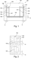
- Fig.1 shows a schematic representation of a device 100 in which an electrical conductor 104 is arranged between an electronic component 110 and a carrier element 101.
- the device 100 is designed to enclose the conductor 104 and at least partially the electronic component 110 in a moisture-tight manner.
- the device 100 has a fiber-reinforced, injection-molded carrier element 101 which has a cavity for receiving the electronic component 110 and consists of a thermoplastic material.
- the device 100 also has the electronic component 110 which is arranged in the cavity.
- a filling compound 102 adheres to the carrier element 101 and the electronic component 110 and is arranged between the electronic component 110 and the carrier element 101.
- the device 100 has an electrical conductor 104 which is coupled to the electronic component 110 and the carrier element 101 and is at least partially surrounded by the filling compound 102.
- the carrier element 101 is in particular a fiber-reinforced, injection-molded component which has sufficient strength and hardness.
- the carrier element 101 has the cavity in which the electronic component 110 is embedded.
- the carrier element 101 and its cavity can be designed such that at least two sides of an electronic component 110 can be covered.
- a cavity can be formed by means of a V-shaped or L-shaped carrier element 101.
- the cavity can also be designed such that at least one side of the component 110 remains free and is not covered by an area of the carrier element 101.
- the carrier element 101 is in particular fiber-reinforced to ensure high strength.
- Fiber-reinforcing materials can be used which, embedded in a polymer matrix, produce a fiber composite.
- the filling compound 102 (potting compound) at least partially envelops the electronic component 110 and forms a fastening of the electronic component 110 in the cavity of the carrier element 101.
- the filling compound 102 adheres in particular to the electronic component 110 and is arranged between the electronic component 110 and the carrier element 101 in order to fasten the electronic component 110 accordingly.
- gas bubbles 103 are present in the carrier element 101.
- the gas bubbles 104 are less than 10 mm away from the filling compound.
- an area is created which extends from a contact surface (surface) 107 of the carrier element with the filling compound 102 at least 10 mm (millimeters) or more into the interior of the carrier element 101.
- the 10 mm can be measured, for example, as a distance x along a perpendicular to the contact surface 107 from the contact surface 107 into the interior of the carrier element 101.
- gas bubbles 103 or cavities Due to the presence of gas bubbles 103 or cavities, corresponding depressions are formed on the contact surface 107 on the surface areas with open gas bubbles 103.
- the introduction of gas bubbles 103 impairs the orientation and formation of the fibers 106, so that after the hardening of the carrier element 101, fiber elements 106 or fiber ends are present on the contact surface 107.
- the proportion of gas bubbles, particularly in a first region 108 of the carrier element, can be set between 1 vol.% (volume percent) and 30 vol.%.
- the strength of the carrier element 101 is thus only insignificantly reduced by the introduction of gas bubbles 103, so that despite the presence of gas bubbles 103 in the carrier element 101, sufficient stability is ensured.
- the contact surface 107 of the carrier element 101 in the contact zone with the filling compound 102 has exposed reinforcing fibers 106 and/or microcrystalline cavities. As described above, this leads to improved adhesion of the filling compound 102. (Glass) fiber stubble and microcavities (gas bubbles 103) are utilized by the casting compound (filling compound 102) as mechanical clamping for improved adhesion.
- the carrier element 101 has, for example, at least two regions 108, 109 with different concentrations of a gas bubble density.
- a first region 108 which represents, for example, the region from the contact surface 107 into the interior of the carrier element, can have a higher density of gas bubbles 103 than a second region 109, which, for example, borders on the first region 108 and is spaced from the contact surface 107.
- the first region 108 which borders on the contact surface 107 and has the higher proportion of gas bubbles, can preferably form the microcavities and the exposed fiber components.
- the deeper second region 109 with a lower density of gas bubbles 103 can, for example, lead to a higher density of the carrier element 101 and thus to, for example, greater durability and hardness of the carrier element 101. Properties of the carrier element 101 can thus be specifically adjusted.
- the contact surface 107 can also be structured more coarsely and in particular have a wave-shaped surface and/or a grooved surface. This increases in particular the contact surface 107 of the carrier element 101 to the filling compound 102 and, for example, the roughness. This leads to a stronger connection between the carrier element 101 and the filling compound 102.
- the cavity of the carrier element 101 can have an opening through which the electronic component 110 protrudes into the environment with a protruding area. Between the protruding area and the carrier element 110 there is at least one area with filling compound 102 such that an inner area of the device 100 is sealed in a liquid-tight manner from the environment of the device.
- the sealing by means of the filling material 102 so that a seal, in particular against liquids, is provided between the internal volume of the device 100 and the environment.
- the carrier element 101 further comprises at least one positioning element 105 against which the electronic component 110 rests and can be positioned.
- the positioning element 105 is, for example, a web or an edge or step in order to form a seat or a support for the electronic component 110.
- the positioning element 105 is, for example, formed integrally with the carrier element 101 and can be manufactured in a common injection molding process.
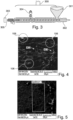
- Fig. 2 shows a sectional view of electrical conductors 104 which penetrate a carrier element 101.
- the electrical conductor is a solid conductor, wherein the solid conductor in particular has a cross-section of 0.1 mm 2 to 10 mm 2 .
- a solid conductor consists in particular of a (monolithic) solid wire or solid sheet.
- the electrical conductor 104 runs through the carrier element 101 for external connection from the electronic component 110, wherein the electrical conductor 104 is electronically coupled to the electronic component 110 by means of soldering, welding, plugging, in particular an insulation displacement connection and/or clamping.
- the electrical conductor 104 penetrates the surface of the carrier element 101 in such a way that this penetration lies in a contact surface 107 from the carrier element 101 to the filling compound 102.
- the gas bubbles 103 are formed, at least in some areas, closer than 10 mm to the electrical conductor 104 in the carrier element 101.
- Fig.3 shows a schematic representation of a manufacturing device 300 according to an exemplary embodiment of the present invention.
- the manufacturing device 300 has, for example, a funnel 301, which feeds the raw material of the carrier element 101 (for example granulate) to an extruder 302.
- the raw material can be heated and mixed so that a homogeneous viscous mass is formed.
- the viscous mass is conveyed by the extruder 302 to a nozzle 305, in particular a needle valve nozzle, through which nozzle 305 the viscous material can be injected into an injection mold 303 at a predetermined temperature, pressure and volume flow.
- a gas injector 304 is also coupled, which introduces a gas, for example inert gas, in particular nitrogen, into the viscous material to form the gas bubbles 103.
- a gas for example inert gas, in particular nitrogen
- the viscous mass is mixed with the injected gas so that a homogeneous gas/viscous mass mixture is formed.
- the gas bubbles 103 are present homogeneously in this mixture.
- the homogeneous gas/viscous mass mixture is injected into the injection mold 303 through the nozzle 305. Due to the variation of the injection pressure, the temperature, and the mass flow with which the homogeneous gas/viscous mass mixture is injected, different areas 108, 109 (see Fig.1 ) with different densities of gas bubbles 103 and in particular different sizes of gas bubbles 103 are generated in the carrier element 101.
- a contact surface of the carrier element with the filling compound has a greater roughness than a corresponding surface of the injection mold, wherein in particular the surface has a microstructure which is at least partially filled with the filling compound, particularly preferably that the filling compound can adhere to fiber stubble.
- the greater roughness of the contact surface of the carrier element 101 is formed in particular by the microstructuring by the gas bubbles 102 and the exposed fibers 106 on the contact surface. This means that even with a smooth surface of the injection mold 303, which is advantageous to prevent adhesion of the assigned material, a rougher contact surface 107 of the carrier element 101 is created in order to provide improved adhesion with the filling compound 102.
- gas injector 304 gas is fed into the extruder 302 and a material of the carrier element 101 is mixed with an inert gas, in particular nitrogen, to form the gas bubbles.
- a gas pressure of between 30 bar and 230 bar can be provided so that the inert gas is injected into a shear and mixing zone in the material of the carrier element 101. Due to the variation in the pressure and, for example, the temperature at which the gas is injected into the viscous mass in the extruder 302, a size of the gas bubbles and a number or density of the gas bubbles 103 in the viscous material can be adjusted.
- a significant holding pressure i.e. a static pressure after injection into the injection mold 303, must be maintained until the polymer melt reaches even the most remote points of the injection mold 303.
- the above-described regions 108, 109 with a higher or a lower gas bubble density in a carrier element 101 can be specifically set.
- Fig.4 shows a schematic representation of an SEM image of a contact surface 107 of a carrier element 101 with gas bubbles 103 according to an exemplary embodiment of the present invention.
- Fig.5 shows for comparison a schematic representation of a SEM image of a contact surface 107 of a carrier element 101 without gas bubbles 103.
- the glass fibers 106 protruding within the circles and the resulting microcavities 401 on the surface are marked with arrows.
- gas bubbles 103 are generated in the carrier element 101 in an injection molding process, glass fibers 106 emerge at the surface and/or microcavities 401 are formed, as shown in Fig.4 shown.
- These glass fiber plugs 106 and microcavities 401 can be used by the filling compound 102 as mechanical clamping for improved adhesion. This improved adhesion of the filling compound 102 thus achieved also allows for particularly good sealing with regard to moisture migration.
- a fiber-reinforced carrier element 101 without gas bubbles 103 As shown, in a fiber-reinforced carrier element 101 with gas bubbles 103 on the surface, pores (microcavities 401) that have come to rest during demolding and protrude into the matrix now open occur. A high number of open pores or microcavities 401 can be seen in comparison to the one in Fig.5 carrier element 101 shown without injected gas bubbles 103.
- the mineral fiber portions 106 lying parallel to the surface also have polar portions for improved adhesion. Mineral fiber ends 106 protruding transversely to the surface also provide mechanical anchoring and polar portions.
Landscapes
- Engineering & Computer Science (AREA)
- Manufacturing & Machinery (AREA)
- Mechanical Engineering (AREA)
- Injection Moulding Of Plastics Or The Like (AREA)
Claims (15)
- Dispositif (100) permettant un coffrage étanche à l'humidité d'un composant électronique (110), le dispositif (100) comprenantun élément de support (101) renforcé de fibres, moulé par injection, qui présente une cavité permettant d'accueillir le composant électronique (110), et qui est constitué d'une matière synthétique thermoplastique,le composant électronique (110), qui est agencé dans la cavité,une masse de remplissage (102) qui adhère à l'élément de support (101) et au composant électronique (110) et qui est agencée entre le composant électronique (110) et l'élément de support (101),un conducteur électrique (104) qui est couplé au composant électronique (110) et à l'élément de support (101) et qui est au moins localement entouré par la masse de remplissage (102),dans lequel l'élément de support (101) contient des bulles de gaz (103) qui sont situées à moins de 10 mm de la masse de remplissage (102).
- Dispositif (100) selon la revendication précédente,
dans lequel la teneur en bulles de gaz est comprise entre 1 % et 30 % en volume, en particulier entre 2 % et 10 % en volume. - Dispositif (100) selon l'une quelconque des revendications précédentes,
dans lequel les bulles de gaz présentent une taille de pores comprise entre 10 et 50 microns. - Dispositif (100) selon l'une quelconque des revendications précédentes,dans lequel l'élément de support (101) présente une proportion de polypropylène ou est en particulier constitué majoritairement de polypropylène,dans lequel en particulier le conducteur électrique (104) pénètre la surface de l'élément de support (101) de telle manière que ladite pénétration se produit dans une surface de contact (107) de l'élément de support (101) par rapport à la masse de remplissage (102),dans lequel les bulles de gaz (103) sont formées à moins de 10 mm, en particulier à moins de 4 mm, en particulier à moins de 2 mm, du conducteur électrique (104),dans lequel les bulles de gaz (103) contiennent en particulier des gaz inertes, en particulier de l'azote.
- Dispositif (100) selon l'une quelconque des revendications précédentes,
dans lequel la surface de contact (107) de l'élément de support (101) dans la région de contact par rapport à la masse de remplissage (102) présente des fibres de renforcement (106) exposées et/ou des cavités microcristallines. - Dispositif (100) selon l'une quelconque des revendications précédentes,
dans lequel l'élément de support (101) présente au moins deux régions (108, 109) avec des concentrations différentes de la densité de bulles de gaz. - Dispositif (100) selon l'une quelconque des revendications précédentes,
dans lequel l'élément de support (101) présente, au sein d'une surface de contact (107) par rapport à la masse de remplissage (102), différents coefficients de frottement statique dans différentes directions le long de la surface de contact (107). - Dispositif (100) selon l'une quelconque des revendications précédentes, présentant en outre au moins une des caractéristiques ci-dessous :l'élément de support (101) présente une surface de contact (107) par rapport à la masse de remplissage (102),la surface de contact (107) est structurée et présente en particulier une surface ondulée et/ou une surface rainurée,la cavité de l'élément porteur (101) présente une ouverture à travers laquelle une région saillante du composant électronique (110) fait saillie dans l'environnement,au moins une région comprenant de la masse de remplissage (102) est présente entre la région saillante et l'élément de support (101) de telle manière qu'une région intérieure du dispositif (100) est scellée de manière étanche aux fluides par rapport à un environnement du dispositif (100),l'élément de support (101) présente au moins un élément de positionnement (105) contre lequel le composant électronique (110) s'appuie et peut être positionné, etl'élément de positionnement (105) présente une cheville de guidage, un rail de guidage ou une piste de guidage au niveau duquel/de laquelle un élément de couplage correspondant du composant électronique (110) peut être couplé.
- Dispositif (100) selon l'une quelconque des revendications précédentes, présentant en outre au moins une des caractéristiques ci-dessous :l'élément de support (101) comprend un polymère présentant un indice de fluidité à chaud inférieur à 5 g/10 min, en particulier inférieur à 1 g/10 min,l'élément de support (101) présente une teneur en fibres en pourcentage en poids comprise entre 5 % et 60 %, en particulier comprise entre 10 % et 50 %, et plus particulièrement comprise entre 15 % et 40 %,l'élément de support (101) présente des fibres de renforcement (106) constituées de fibres minérales, en particulier de silicates, de verre, de basalte, d'amiante, de wollastonite, de fibres de carbone, en particulier de nanotubes de carbone, de fibres polymères, en particulier de fibres de polyamide, de fibres de polyimide, de polyester, de polyoléfines, de polyesteramides, d'aramides, en particulier de kevlar, et/ou de fibres naturelles, en particulier de cellulose, de coton, de viscose, de lyocell, de bois, de chanvre, de soie, etles fibres de renforcement (106) présentent des fibres longues d'une longueur comprise entre 1 mm et 20 mm, en particulier comprise entre 5 mm et 15 mm.
- Dispositif (100) selon l'une quelconque des revendications précédentes, présentant en outre au moins une des caractéristiques ci-dessous :la masse de remplissage (102) comprend du polyuréthane ou de la résine époxy,le conducteur électrique (104) est un conducteur plein,le conducteur plein présente en particulier une section comprise entre 0,1 mm2 et 10 mm2,le conducteur électrique (104) menant au raccordement externe du composant électronique (110) passe à travers l'élément de support (101),le conducteur électrique (104) est couplé électroniquement au composant électronique (110) par brasage, par soudage, par enfichage, en particulier d'un connecteur autodénudant, et/ou par coincement,le composant électronique (110) est un microrupteur, un actionneur, une résistance ou un capteur, en particulier un capteur de température ou un capteur de distance, etl'élément de support (101) pèse moins de 1 kg.
- Procédé de fabrication d'un dispositif (100) selon l'une quelconque des revendications 1 à 10 permettant un coffrage étanche à l'humidité d'un conducteur (104) d'un composant électronique (110), le procédé comprenant les étapes consistant àmouler par injection un élément de support (101) constitué d'une matière thermoplastique, renforcé de fibres et présentant une cavité permettant d'accueillir le composant électronique (110),agencer le composant électronique (110) dans la cavité,coupler un conducteur électrique (104) au composant électronique (110) et à l'élément de support (101),remplir une masse de remplissage (102) entre le composant électronique (110) et l'élément de support (101),dans lequel la masse de remplissage (102) adhère à l'élément de support (101) et au composant électronique (110),dans lequel le conducteur électrique (104) est entouré au moins localement par la masse de remplissage (102),dans lequel l'élément de support (101) contient des bulles de gaz (103) situées à moins de 10 mm de la masse de remplissage (102).
- Procédé selon la revendication 11,dans lequel l'étape de moulage par injection comprend les étapes consistant àmélanger un matériau de l'élément de support (101) avec un gaz inerte, en particulier de l'azote, afin de former les bulles de gaz (103),introduire le matériau comprenant les bulles de gaz (103) dans un moule d'injection (303),dans lequel une surface de contact (107) de l'élément porteur (101) par rapport à la masse de remplissage (102) présente en particulier une rugosité supérieure à celle d'une surface correspondante du moule d'injection (303),dans lequel la surface présente en particulier une microstructuration qui est au moins partiellement remplie avec la masse de remplissage (102),dans lequel la masse de remplissage peut de manière particulièrement préférée adhérer aux bourres de fibres.
- Procédé selon la revendication 12,
dans lequel, lors de l'étape de mélange, un gaz inerte, en particulier de l'azote, est introduit avec une pression de gaz comprise entre 30 bars et 230 bars, en particulier comprise entre 80 bars et 160 bars, de sorte que le gaz inerte est injecté dans le matériau de l'élément de support (101) dans une zone de cisaillement et de mélange. - Procédé selon la revendication 12 ou 13,
dans lequel une capacité d'injection d'au plus 1 kg est mise en œuvre lors de l'étape d'introduction du matériau de l'élément de support (101) dans le moule d'injection (303). - Procédé selon l'une quelconque des revendications 12 à 14,
dans lequel le gaz inerte se trouve dans un état supercritique, en particulier au moins temporairement, lors de l'étape de mélange.
Applications Claiming Priority (2)
| Application Number | Priority Date | Filing Date | Title |
|---|---|---|---|
| DE102020121179.1A DE102020121179B3 (de) | 2020-08-12 | 2020-08-12 | Elektrischer Komponententräger |
| PCT/EP2021/072347 WO2022034122A1 (fr) | 2020-08-12 | 2021-08-11 | Porteur de composant électrique |
Publications (3)
| Publication Number | Publication Date |
|---|---|
| EP4196331A1 EP4196331A1 (fr) | 2023-06-21 |
| EP4196331C0 EP4196331C0 (fr) | 2024-08-07 |
| EP4196331B1 true EP4196331B1 (fr) | 2024-08-07 |
Family
ID=77519112
Family Applications (1)
| Application Number | Title | Priority Date | Filing Date |
|---|---|---|---|
| EP21762018.6A Active EP4196331B1 (fr) | 2020-08-12 | 2021-08-11 | Porteur de composant électrique |
Country Status (3)
| Country | Link |
|---|---|
| EP (1) | EP4196331B1 (fr) |
| DE (1) | DE102020121179B3 (fr) |
| WO (1) | WO2022034122A1 (fr) |
Families Citing this family (1)
| Publication number | Priority date | Publication date | Assignee | Title |
|---|---|---|---|---|
| DE102024126877A1 (de) * | 2024-09-19 | 2026-03-19 | Bayerische Motoren Werke Aktiengesellschaft | Verfahren zur Herstellung eines Batteriemoduls, Batteriemodul sowie ein Fahrzeug mit einem solchen Batteriemodul |
Family Cites Families (5)
| Publication number | Priority date | Publication date | Assignee | Title |
|---|---|---|---|---|
| US8107207B2 (en) * | 2008-08-08 | 2012-01-31 | Surge Suppression Incorporated | Potted electrical circuit with protective insulation |
| DE202007003687U1 (de) | 2007-03-09 | 2008-07-10 | Pepperl + Fuchs Gmbh | Anordnung mit Gehäuse, elektronischen Bauelementen und Vergussmasse |
| DE102011004694A1 (de) * | 2011-02-24 | 2012-08-30 | Robert Bosch Gmbh | Schaltungsanordnung, insbesondere ein Getriebesteuergerät, mit mindestens einem Deckel zur Kapselung eines Schaltungsträgers |
| KR102204791B1 (ko) * | 2014-04-16 | 2021-01-20 | 사빅 글로벌 테크놀러지스 비.브이. | 긴 유리 섬유 충전재에서의 발포 기술 |
| US10161733B2 (en) * | 2017-04-18 | 2018-12-25 | Dynaenergetics Gmbh & Co. Kg | Pressure bulkhead structure with integrated selective electronic switch circuitry, pressure-isolating enclosure containing such selective electronic switch circuitry, and methods of making such |
-
2020
- 2020-08-12 DE DE102020121179.1A patent/DE102020121179B3/de not_active Expired - Fee Related
-
2021
- 2021-08-11 EP EP21762018.6A patent/EP4196331B1/fr active Active
- 2021-08-11 WO PCT/EP2021/072347 patent/WO2022034122A1/fr not_active Ceased
Also Published As
| Publication number | Publication date |
|---|---|
| WO2022034122A1 (fr) | 2022-02-17 |
| EP4196331C0 (fr) | 2024-08-07 |
| DE102020121179B3 (de) | 2021-10-14 |
| EP4196331A1 (fr) | 2023-06-21 |
Similar Documents
| Publication | Publication Date | Title |
|---|---|---|
| DE102009008457A1 (de) | Verfahren zur Herstellung eines Sensors mit nahtloser Umspritzung eines Sensorelementes | |
| DE102009046164A1 (de) | Verfahren zur Herstellung eines Mehrkomponenten-Wischerarms | |
| EP1194476A1 (fr) | Matiere thermoplastique renforcee par de longues fibres et son procede de production | |
| WO2020030375A1 (fr) | Pièce hybride et procédé de production d'une pièce hybride | |
| EP4196331B1 (fr) | Porteur de composant électrique | |
| WO2014076061A1 (fr) | Pièce moulée par injection et outil ainsi que procédé de fabrication | |
| EP3275052B1 (fr) | Composant de réseau de bord pour un véhicule, véhicule équipé d'une telle composant et son procédé de fabrication | |
| EP0982111A2 (fr) | Dispositif et procédé pour encapsuler des circuits électriques par moulage par injection | |
| DE602006000223T2 (de) | Elektronisches Gerät und Verfahren zur Herstellung desselben | |
| EP4161804B1 (fr) | Composant électronique résistant aux vibrations | |
| WO2011042005A2 (fr) | Traversée de câble dans des boîtiers de connecteurs | |
| DE19910973C1 (de) | Verfahren zur Herstellung von drehbar miteinander verbundenen Spritzgußteilen | |
| WO2025067610A1 (fr) | Pièce moulée en matière plastique moulée par injection, procédé de fabrication de la pièce moulée, insert pour la mise en œuvre du procédé et moule d'injection pour la mise en œuvre dudit procédé | |
| EP4049821B1 (fr) | Pièce composite et procédé de fabrication d'une pièce composite | |
| DE102015115793A1 (de) | Herstellung von Objekten mit faserverstärktem Bereich | |
| DE102018215660A1 (de) | Spritzgießwerkzeug zur Herstellung von Spritzgussbauteilen, sowie Verfahren zur Herstellung von Spritzgussbauteilen | |
| DE102020206058A1 (de) | Verbindungselement, Bauteil aus einem Kompositwerkstoff und Verfahren zur Herstellung eines Bauteils aus einem Kompositwerkstoff | |
| WO2000002070A2 (fr) | Férule pour raccord optique enfichable | |
| DE19936956B4 (de) | Verfahren zum Herstellen eines Kunststofformteils | |
| DE102013212257B4 (de) | Verfahren und Vorrichtung zur Herstellung einer mediendichten Umspritzung eines elektrischen Anschlusselements einer Aktoreinheit | |
| DE102023135555B4 (de) | Form, Anordnung und Verfahren zur Herstellung eines Kabelbaums | |
| DE202013100463U1 (de) | Polymerkabelbaum | |
| DE102013020258A1 (de) | Verfahren und Werkzeug zum Herstellen eines Faserverbundbauteils sowie Faserverbundbauteil | |
| DE102017111146B4 (de) | Verfahren zum herstellen eines faserformteils mit integrierter verbindungsbuchse | |
| DE102023208529A1 (de) | Verfahren zur Herstellung eines elektrischen Leitungssatzes sowie elektrischer Leitungssatz |
Legal Events
| Date | Code | Title | Description |
|---|---|---|---|
| STAA | Information on the status of an ep patent application or granted ep patent |
Free format text: STATUS: UNKNOWN |
|
| STAA | Information on the status of an ep patent application or granted ep patent |
Free format text: STATUS: THE INTERNATIONAL PUBLICATION HAS BEEN MADE |
|
| PUAI | Public reference made under article 153(3) epc to a published international application that has entered the european phase |
Free format text: ORIGINAL CODE: 0009012 |
|
| STAA | Information on the status of an ep patent application or granted ep patent |
Free format text: STATUS: REQUEST FOR EXAMINATION WAS MADE |
|
| 17P | Request for examination filed |
Effective date: 20230111 |
|
| AK | Designated contracting states |
Kind code of ref document: A1 Designated state(s): AL AT BE BG CH CY CZ DE DK EE ES FI FR GB GR HR HU IE IS IT LI LT LU LV MC MK MT NL NO PL PT RO RS SE SI SK SM TR |
|
| DAV | Request for validation of the european patent (deleted) | ||
| DAX | Request for extension of the european patent (deleted) | ||
| GRAP | Despatch of communication of intention to grant a patent |
Free format text: ORIGINAL CODE: EPIDOSNIGR1 |
|
| STAA | Information on the status of an ep patent application or granted ep patent |
Free format text: STATUS: GRANT OF PATENT IS INTENDED |
|
| INTG | Intention to grant announced |
Effective date: 20240227 |
|
| GRAS | Grant fee paid |
Free format text: ORIGINAL CODE: EPIDOSNIGR3 |
|
| GRAA | (expected) grant |
Free format text: ORIGINAL CODE: 0009210 |
|
| STAA | Information on the status of an ep patent application or granted ep patent |
Free format text: STATUS: THE PATENT HAS BEEN GRANTED |
|
| AK | Designated contracting states |
Kind code of ref document: B1 Designated state(s): AL AT BE BG CH CY CZ DE DK EE ES FI FR GB GR HR HU IE IS IT LI LT LU LV MC MK MT NL NO PL PT RO RS SE SI SK SM TR |
|
| REG | Reference to a national code |
Ref country code: GB Ref legal event code: FG4D Free format text: NOT ENGLISH |
|
| REG | Reference to a national code |
Ref country code: CH Ref legal event code: EP |
|
| REG | Reference to a national code |
Ref country code: IE Ref legal event code: FG4D Free format text: LANGUAGE OF EP DOCUMENT: GERMAN |
|
| REG | Reference to a national code |
Ref country code: DE Ref legal event code: R096 Ref document number: 502021004722 Country of ref document: DE |
|
| U01 | Request for unitary effect filed |
Effective date: 20240820 |
|
| U07 | Unitary effect registered |
Designated state(s): AT BE BG DE DK EE FI FR IT LT LU LV MT NL PT RO SE SI Effective date: 20240902 |
|
| U20 | Renewal fee for the european patent with unitary effect paid |
Year of fee payment: 4 Effective date: 20240828 |
|
| PG25 | Lapsed in a contracting state [announced via postgrant information from national office to epo] |
Ref country code: NO Free format text: LAPSE BECAUSE OF FAILURE TO SUBMIT A TRANSLATION OF THE DESCRIPTION OR TO PAY THE FEE WITHIN THE PRESCRIBED TIME-LIMIT Effective date: 20241107 |
|
| PG25 | Lapsed in a contracting state [announced via postgrant information from national office to epo] |
Ref country code: GR Free format text: LAPSE BECAUSE OF FAILURE TO SUBMIT A TRANSLATION OF THE DESCRIPTION OR TO PAY THE FEE WITHIN THE PRESCRIBED TIME-LIMIT Effective date: 20241108 Ref country code: PL Free format text: LAPSE BECAUSE OF FAILURE TO SUBMIT A TRANSLATION OF THE DESCRIPTION OR TO PAY THE FEE WITHIN THE PRESCRIBED TIME-LIMIT Effective date: 20240807 |
|
| PG25 | Lapsed in a contracting state [announced via postgrant information from national office to epo] |
Ref country code: IS Free format text: LAPSE BECAUSE OF FAILURE TO SUBMIT A TRANSLATION OF THE DESCRIPTION OR TO PAY THE FEE WITHIN THE PRESCRIBED TIME-LIMIT Effective date: 20241207 |
|
| PG25 | Lapsed in a contracting state [announced via postgrant information from national office to epo] |
Ref country code: HR Free format text: LAPSE BECAUSE OF FAILURE TO SUBMIT A TRANSLATION OF THE DESCRIPTION OR TO PAY THE FEE WITHIN THE PRESCRIBED TIME-LIMIT Effective date: 20240807 |
|
| PG25 | Lapsed in a contracting state [announced via postgrant information from national office to epo] |
Ref country code: RS Free format text: LAPSE BECAUSE OF FAILURE TO SUBMIT A TRANSLATION OF THE DESCRIPTION OR TO PAY THE FEE WITHIN THE PRESCRIBED TIME-LIMIT Effective date: 20241107 Ref country code: ES Free format text: LAPSE BECAUSE OF FAILURE TO SUBMIT A TRANSLATION OF THE DESCRIPTION OR TO PAY THE FEE WITHIN THE PRESCRIBED TIME-LIMIT Effective date: 20240807 |
|
| PG25 | Lapsed in a contracting state [announced via postgrant information from national office to epo] |
Ref country code: RS Free format text: LAPSE BECAUSE OF FAILURE TO SUBMIT A TRANSLATION OF THE DESCRIPTION OR TO PAY THE FEE WITHIN THE PRESCRIBED TIME-LIMIT Effective date: 20241107 Ref country code: PL Free format text: LAPSE BECAUSE OF FAILURE TO SUBMIT A TRANSLATION OF THE DESCRIPTION OR TO PAY THE FEE WITHIN THE PRESCRIBED TIME-LIMIT Effective date: 20240807 Ref country code: NO Free format text: LAPSE BECAUSE OF FAILURE TO SUBMIT A TRANSLATION OF THE DESCRIPTION OR TO PAY THE FEE WITHIN THE PRESCRIBED TIME-LIMIT Effective date: 20241107 Ref country code: IS Free format text: LAPSE BECAUSE OF FAILURE TO SUBMIT A TRANSLATION OF THE DESCRIPTION OR TO PAY THE FEE WITHIN THE PRESCRIBED TIME-LIMIT Effective date: 20241207 Ref country code: HR Free format text: LAPSE BECAUSE OF FAILURE TO SUBMIT A TRANSLATION OF THE DESCRIPTION OR TO PAY THE FEE WITHIN THE PRESCRIBED TIME-LIMIT Effective date: 20240807 Ref country code: GR Free format text: LAPSE BECAUSE OF FAILURE TO SUBMIT A TRANSLATION OF THE DESCRIPTION OR TO PAY THE FEE WITHIN THE PRESCRIBED TIME-LIMIT Effective date: 20241108 Ref country code: ES Free format text: LAPSE BECAUSE OF FAILURE TO SUBMIT A TRANSLATION OF THE DESCRIPTION OR TO PAY THE FEE WITHIN THE PRESCRIBED TIME-LIMIT Effective date: 20240807 |
|
| REG | Reference to a national code |
Ref country code: CH Ref legal event code: PL |
|
| PG25 | Lapsed in a contracting state [announced via postgrant information from national office to epo] |
Ref country code: SM Free format text: LAPSE BECAUSE OF FAILURE TO SUBMIT A TRANSLATION OF THE DESCRIPTION OR TO PAY THE FEE WITHIN THE PRESCRIBED TIME-LIMIT Effective date: 20240807 |
|
| PG25 | Lapsed in a contracting state [announced via postgrant information from national office to epo] |
Ref country code: CH Free format text: LAPSE BECAUSE OF NON-PAYMENT OF DUE FEES Effective date: 20240831 |
|
| PG25 | Lapsed in a contracting state [announced via postgrant information from national office to epo] |
Ref country code: CZ Free format text: LAPSE BECAUSE OF FAILURE TO SUBMIT A TRANSLATION OF THE DESCRIPTION OR TO PAY THE FEE WITHIN THE PRESCRIBED TIME-LIMIT Effective date: 20240807 |
|
| PG25 | Lapsed in a contracting state [announced via postgrant information from national office to epo] |
Ref country code: SK Free format text: LAPSE BECAUSE OF FAILURE TO SUBMIT A TRANSLATION OF THE DESCRIPTION OR TO PAY THE FEE WITHIN THE PRESCRIBED TIME-LIMIT Effective date: 20240807 |
|
| PLBE | No opposition filed within time limit |
Free format text: ORIGINAL CODE: 0009261 |
|
| STAA | Information on the status of an ep patent application or granted ep patent |
Free format text: STATUS: NO OPPOSITION FILED WITHIN TIME LIMIT |
|
| PG25 | Lapsed in a contracting state [announced via postgrant information from national office to epo] |
Ref country code: MC Free format text: LAPSE BECAUSE OF FAILURE TO SUBMIT A TRANSLATION OF THE DESCRIPTION OR TO PAY THE FEE WITHIN THE PRESCRIBED TIME-LIMIT Effective date: 20240807 |
|
| 26N | No opposition filed |
Effective date: 20250508 |
|
| PG25 | Lapsed in a contracting state [announced via postgrant information from national office to epo] |
Ref country code: IE Free format text: LAPSE BECAUSE OF NON-PAYMENT OF DUE FEES Effective date: 20240811 |
|
| U20 | Renewal fee for the european patent with unitary effect paid |
Year of fee payment: 5 Effective date: 20250818 |
|
| PG25 | Lapsed in a contracting state [announced via postgrant information from national office to epo] |
Ref country code: CY Free format text: LAPSE BECAUSE OF FAILURE TO SUBMIT A TRANSLATION OF THE DESCRIPTION OR TO PAY THE FEE WITHIN THE PRESCRIBED TIME-LIMIT; INVALID AB INITIO Effective date: 20210811 |
|
| PG25 | Lapsed in a contracting state [announced via postgrant information from national office to epo] |
Ref country code: HU Free format text: LAPSE BECAUSE OF FAILURE TO SUBMIT A TRANSLATION OF THE DESCRIPTION OR TO PAY THE FEE WITHIN THE PRESCRIBED TIME-LIMIT; INVALID AB INITIO Effective date: 20210811 |