EP4195253A1 - Semiconductor structure forming method and semiconductor structure - Google Patents
Semiconductor structure forming method and semiconductor structure Download PDFInfo
- Publication number
- EP4195253A1 EP4195253A1 EP21871094.5A EP21871094A EP4195253A1 EP 4195253 A1 EP4195253 A1 EP 4195253A1 EP 21871094 A EP21871094 A EP 21871094A EP 4195253 A1 EP4195253 A1 EP 4195253A1
- Authority
- EP
- European Patent Office
- Prior art keywords
- conductive
- layers
- contact
- forming
- layer
- Prior art date
- Legal status (The legal status is an assumption and is not a legal conclusion. Google has not performed a legal analysis and makes no representation as to the accuracy of the status listed.)
- Pending
Links
Images






Classifications
-
- H—ELECTRICITY
- H10—SEMICONDUCTOR DEVICES; ELECTRIC SOLID-STATE DEVICES NOT OTHERWISE PROVIDED FOR
- H10B—ELECTRONIC MEMORY DEVICES
- H10B12/00—Dynamic random access memory [DRAM] devices
- H10B12/01—Manufacture or treatment
- H10B12/02—Manufacture or treatment for one transistor one-capacitor [1T-1C] memory cells
- H10B12/03—Making the capacitor or connections thereto
- H10B12/033—Making the capacitor or connections thereto the capacitor extending over the transistor
- H10B12/0335—Making a connection between the transistor and the capacitor, e.g. plug
-
- H—ELECTRICITY
- H10—SEMICONDUCTOR DEVICES; ELECTRIC SOLID-STATE DEVICES NOT OTHERWISE PROVIDED FOR
- H10B—ELECTRONIC MEMORY DEVICES
- H10B12/00—Dynamic random access memory [DRAM] devices
- H10B12/01—Manufacture or treatment
- H10B12/02—Manufacture or treatment for one transistor one-capacitor [1T-1C] memory cells
-
- H—ELECTRICITY
- H10—SEMICONDUCTOR DEVICES; ELECTRIC SOLID-STATE DEVICES NOT OTHERWISE PROVIDED FOR
- H10B—ELECTRONIC MEMORY DEVICES
- H10B12/00—Dynamic random access memory [DRAM] devices
- H10B12/30—DRAM devices comprising one-transistor - one-capacitor [1T-1C] memory cells
- H10B12/48—Data lines or contacts therefor
- H10B12/482—Bit lines
-
- H—ELECTRICITY
- H10—SEMICONDUCTOR DEVICES; ELECTRIC SOLID-STATE DEVICES NOT OTHERWISE PROVIDED FOR
- H10B—ELECTRONIC MEMORY DEVICES
- H10B12/00—Dynamic random access memory [DRAM] devices
- H10B12/30—DRAM devices comprising one-transistor - one-capacitor [1T-1C] memory cells
-
- H—ELECTRICITY
- H10—SEMICONDUCTOR DEVICES; ELECTRIC SOLID-STATE DEVICES NOT OTHERWISE PROVIDED FOR
- H10B—ELECTRONIC MEMORY DEVICES
- H10B12/00—Dynamic random access memory [DRAM] devices
- H10B12/30—DRAM devices comprising one-transistor - one-capacitor [1T-1C] memory cells
- H10B12/31—DRAM devices comprising one-transistor - one-capacitor [1T-1C] memory cells having a storage electrode stacked over the transistor
- H10B12/315—DRAM devices comprising one-transistor - one-capacitor [1T-1C] memory cells having a storage electrode stacked over the transistor with the capacitor higher than a bit line
-
- H—ELECTRICITY
- H10—SEMICONDUCTOR DEVICES; ELECTRIC SOLID-STATE DEVICES NOT OTHERWISE PROVIDED FOR
- H10B—ELECTRONIC MEMORY DEVICES
- H10B12/00—Dynamic random access memory [DRAM] devices
- H10B12/30—DRAM devices comprising one-transistor - one-capacitor [1T-1C] memory cells
- H10B12/48—Data lines or contacts therefor
- H10B12/485—Bit line contacts
Definitions
- the present disclosure relates to the field of semiconductors, and in particular to a method for forming a semiconductor structure and a semiconductor structure.
- DRAM dynamic random access memory
- the electrical connection between a transistor and a capacitor needs to be achieved by depositing a capacitor contact structure, in which a resistance of the capacitor contact structure formed by depositing affects a current between the transistor and the capacitor, thereby affecting the electrical conductivity of a device.
- An existing method for forming a capacitor contact structure cannot effectively reduce a resistance of the formed capacitor contact structure, so that the electrical conductivity of the formed DRAM is affected.
- Embodiments of the present disclosure provide a method for forming a semiconductor structure, including the following operations.
- a semiconductor substrate is provided, on which bit line structures and dielectric layers that are discretely arranged are formed, in which an extension direction of the dielectric layers is intersected with an extension direction of the bit line structures, and the bit line structures and the dielectric layers jointly define discrete capacitor contact openings.
- First conductive layers for filling the capacitor contact openings are formed, in which top surfaces of the first conductive layers are lower than top surfaces of the bit line structures.
- Conductive contact layers located on the top surfaces of the first conductive layers are formed, in which a thickness of a first part and/or a thickness of a second part of each conductive contact layer is greater than a thickness of a third part thereof.
- the first part is a part of a conductive contact layer in contact with a bit line structure
- the second part is a part of the conductive contact layer in contact with the dielectric layer
- the first part, the second part and the third part together constitute the conductive contact layer.
- Second conductive layers that are discretely arranged and electrically connected with the conductive contact layers are formed, in which the second conductive layers are configured to adjust an arrangement mode of capacitor contact structures formed by filling the capacitor contact openings.
- Embodiments of the present disclosure further provide a semiconductor structure, including a semiconductor substrate, first conductive layers, conductive contact layers and second conductive layers.
- Bit line structures and dielectric layers are provided on the semiconductor substrate, an extension direction of the dielectric layers is intersected with an extension direction of the bit line structures, and the bit line structures and the dielectric layers jointly define discrete capacitor contact openings.
- the first conductive layers are located at the bottoms of the capacitor contact openings, and top surfaces of the first conductive layers are lower than top surfaces of the bit line structures.
- the conductive contact layers are located on the top surfaces of the first conductive layers.
- a thickness of a first part and/or a thickness of a second part of each conductive contact layer is greater than a thickness of a third part thereof, in which the first part is a contact part of a conductive contact layer in contact with a bit line structure, the second part is a contact part of the conductive contact layer in contact with the dielectric layer, and the first part, the second part and the third part together constitute the conductive contact layer.
- the second conductive layers are electrically connected with the conductive contact layers, and configured to adjust an arrangement mode of capacitor contact structures formed by filling the capacitive contact openings.
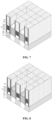
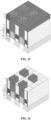
- FIGs. 1-22 are structure schematic diagrams corresponding to each operation of a method for forming a semiconductor structure provided by the embodiments of the present disclosure.
- a method for forming a capacitor contact structure in a related art cannot effectively reduce a resistance of the formed capacitor contact structure, thereby affecting the electrical conductivity of the formed DRAM.
- the embodiments of the present disclosure provide a method for forming a semiconductor structure, including the following operations.
- a semiconductor substrate is provided, on which bit line structures and dielectric layers that are discretely arranged are formed, in which an extension direction of the dielectric layers is intersected with an extension direction of the bit line structures, and the bit line structures and the dielectric layers jointly define discrete capacitor contact openings.
- First conductive layers for filling the capacitor contact openings are formed, in which top surfaces of the first conductive layers are lower than top surfaces of the bit line structures.
- Conductive contact layers located on the top surfaces of the first conductive layers are formed, in which a thickness of a first part and/or a thickness of a second part of each conductive contact layer is greater than a thickness of a third part thereof.
- the first part is a contact part of a conductive contact layer in contact with a bit line structure
- the second part is a contact part of the conductive contact layer in contact with the dielectric layer
- the first part, the second part and the third part together constitute the conductive contact layer.
- Second conductive layers that are discretely arranged and electrically connected with the conductive contact layers are formed, in which the second conductive layers are configured to adjust an arrangement mode of capacitor contact structures formed by filling the capacitor contact openings.
- FIGs. 1-22 are structure schematic diagrams corresponding to each operation of a method for forming a semiconductor structure provided by embodiments of the present disclosure, and the method for forming a semiconductor structure of the embodiments of the present disclosure is described in detail below.
- a semiconductor substrate 101 is provided, on which bit line structures 102 and dielectric layers 103 that are discretely arranged are formed, in which an extension direction of the dielectric layers 103 is intersected with an extension direction of the bit line structures 102, and the bit line structures 102 and the dielectric layers jointly define discrete capacitor contact openings 104.
- Each bit line structure 102 includes a bottom dielectric layer (not shown), a bit line contact layer 112, a metal layer 122, and a top dielectric layer 132 stacked sequentially.
- the material of the bit line contact layers 112 includes tungsten or polysilicon.
- the materials of the bottom dielectric layers (not shown) and the top dielectric layers 135 include silicon nitride, silicon dioxide or silicon oxynitride.
- the metal layers 122 may be composed of one conductive material or a plurality of conductive materials, such as doped polysilicon, titanium, titanium nitride, tungsten, a tungsten complex and the like.
- the material of the dielectric layers 103 includes silicon nitride, silicon dioxide, or silicon oxynitride. In an embodiment of the present disclosure, the material of the dielectric layers 103 may be the same as the material of the top dielectric layers 132.
- top surfaces and sidewalls of bit line structures 102 are further covered with a protection structure, in which the protection structure is configured to electrically isolate the bit line structures 102 from the capacitor contact structures formed subsequently.
- the protection structure is a laminated structure including a top dielectric layer 132, a second dielectric layer 142, and a third dielectric layer 152 that are sequentially formed on the sidewall of a bit line structure, in which the material of the third dielectric layer 152 may be the same as the material of the top dielectric layer 132, and the material of the second dielectric layer 142 and the material of the top dielectric layer 132 may be different.
- the protection structure is implemented in a laminated structure so as to have a better electrical isolation effect, and is configured to reduce parasitic resistance between bit line structures 102 and capacitor contact structures formed subsequently.
- capacitor contact openings 104 Areas defined by adjacent bit line structures 102 and adjacent dielectric layers 103 serves as the capacitor contact openings 104 which are configured to form the capacitor contact structures subsequently.
- first conductive layers 201 filling the capacitor contact openings 104 are formed, in which top surfaces of the first conductive layers 201 are lower than top surfaces of the bit line structures 102.
- a first conductive film (not shown) filling capacitor contact openings 104 is formed, in which the first conductive film (not shown) covers the bit line structures 102 and the dielectric layers 103.
- the first conductive film (not shown) is etched, until discrete first conductive structures 211 are formed.
- the first conductive film (not shown) is etched by chemical mechanical polishing, until top surfaces of the bit line structures 102 and the dielectric layers 103 are exposed, as to form the first conductive structures 211.
- the top of the first conductive film (not shown) is polished by chemical mechanical polishing, as to form the first conductive structures 211 discretely arranged.
- the chemical mechanical polishing has a higher removal rate compared to an etching process, and is beneficial to shorten a process period.
- the first conductive structures 211 of a partial thickness are etched to form the first conductive layers 201.
- the first conductive layers 201 are bottom conductive layers of the capacitor contact structures formed subsequently, and are configured to electrically connect with the active areas 111 in the semiconductor substrate 101, and the material of the first conductive layers 201 includes semiconductor conductive materials such as doped polysilicon and polysilicon. In an embodiment of the present disclosure, the material of the first conductive layers 201 is doped polysilicon.
- each formed first conductive layer 201 has a groove.
- the groove 205 is formed in a first conductive layer 201, in which the groove 205 is located in a position of the first conductive layer 201 in contact with the bit line structures 102, and in a position of the first conductive layer 201 in contact with the dielectric layers 103.
- a method for forming the grooves 205 is as the follows.
- a first sacrificial layer 202 located on the tops and sidewalls of the bit line structures 102, the tops and sidewalls of the dielectric layers 103 and the tops of the first conductive layers 201 is formed.
- the material of the first sacrificial layer 202 is different from the materials of the dielectric layers 103 and the first conductive layers 201, so that it is selectively removed subsequently by etching using a wet etching technology.
- the material of the first sacrificial layer 202 is silicon oxide.
- Barrier layers 203 for filling the capacitor contact openings 104 are formed.
- the material of the barrier layers 203 may be a photoresist.
- forming the barrier layers 203 includes the following operations.
- a barrier film (not shown) for filling the capacitor contact openings 104 is formed, in which a top surface of the barrier film (not shown) is higher than a top surface of the first sacrificial layer 202.
- the barrier film (not shown) is etched, so as to form the discrete barrier layers 203.
- the barrier film (not shown) is etched by chemical mechanical polishing, so as to form the barrier layers 203.
- the top of the barrier film (not shown) is polished by the chemical mechanical polishing, as to form the barrier layers 203 that are discretely arranged.
- the chemical mechanical polishing has a higher removal rate compared to an etching process, and is beneficial to shorten the process period.
- the first sacrificial layer located on the tops and sidewalls of the bit line structures 102 and the tops and sidewalls of the dielectric layers 103 is etched with the barrier layers 203 as a mask to form through holes (not shown), in which the first conductive layers 201 are exposed, A part of the first conductive layers 201 is etched on the basis of the through holes (not shown), as to form the grooves 205.
- the barrier layers 203 (referring to FIG. 4 ) and the remaining first sacrificial layer 202 (referring to FIG. 4 ) are moved.
- conductive contact layers 206 located on the top surfaces of the first conductive layers 201 are formed.
- a thickness of a first part and/or a thickness of a second part of each conductive contact layer 206 are greater than a thickness of a third part thereof.
- the first part is a part of a conductive contact layer 206 in contact with bit line structures 102
- the second part is a part of the conductive contact layer 206 in contact with dielectric layers 103
- the third part is a middle part of the conductive contact layer 206
- each conductive contact layer 206 consist of the first part, the second part and the third part.
- the conductive contact layers 206 are formed, so as to increase contact areas between the first conductive layers 201 and the second conductive layers formed subsequently, thereby reducing the resistance of the capacitor contact structures formed subsequently.
- Embodiments of the present disclosure provide three different methods for forming the conductive contact layers 206 thereby forming the conductive contact layers 206 with different morphologies.
- the conductive contact layers 206 are formed by the first method, no groove 205 needs to be formed in the first conductive layers 201, namely the first method is implemented on the basis of FIG. 3 .
- the grooves 205 need to be formed in the first conductive layers 201, namely the second method and the third method are implemented on the basis of FIG. 5 .
- the conductive contact layers 206 located on the tops of the first conductive layers 201 are formed, in which top surfaces of the conductive contact layers 206 are higher than top surfaces of the bit line structures 102. Forming the conductive contact layers 206 includes the following operations.
- a conductive contact film 216 covering the top surfaces of the first conductive layers 201, the top surfaces and sidewalls of the bit line structures 102, the top surfaces and sidewalls of the dielectric layers 103 is formed, and second sacrificial layers 207 for filling openings in the conductive contact film 216 are formed.
- the conductive contact film 216 is configured to form the conductive contact layers 206 subsequently.
- the material of the conductive contact film 216 is titanium nitride.
- a part of the conductive contact film 216 is removed by etching with the second sacrificial layers 207 as a mask to form the conductive contact layers 206 and etched through holes for exposing the conductive contact layers.
- the bottom surface of each etched through hole is higher than the top surface of each second sacrificial layer 207. Namely the height of the first part and the height of a second part of each etched through hole formed are higher than the height of a third part thereof.
- the second sacrificial layers 207 are removed.
- the morphology of the formed conductive contact layers 206 is as shown in FIG. 8 .
- the conductive contact layers 206 for filling the grooves 205 and covering the first conductive layers 201 are formed, in which the top surfaces of the conductive contact layers 206 are higher than the top surfaces of the bit line structures 102.
- Forming the conductive contact layers 206 includes the following operations.
- the conductive contact film 216 for covering the top surfaces of the first conductive layers 201, the top surfaces and sidewalls of the bit line structures 102, and the top surfaces and sidewalls of the dielectric layers 103, and filling the grooves 205 is formed, and the second sacrificial layers 207 for filling the openings in the conductive contact film 216 are formed.
- a part of the conductive contact film 216 is removed by etching with the second sacrificial layers 207 as a mask to form the conductive contact layers 206 and etched through holes for exposing the conductive contact layers.
- the bottom surface of each etched through hole is higher than the top surface of each second sacrificial layer 207. Namely, the height of the first part and the height of the second part of each formed etched through hole are higher than the height of the third part thereof.
- the second sacrificial layers 207 are removed.
- the morphology of the formed conductive contact layers 206 is as shown in FIG. 11 .
- the conductive contact layers 206 for filling the grooves 205 and covering the first conductive layers 201 are formed, in which the top surfaces of the conductive contact layers 206 are higher than the top surfaces of the bit line structures 102.
- the forming the conductive contact layers 206 includes the following operations.
- the conductive contact film 216 for covering the top surfaces of the first conductive layers 201, the top surfaces and sidewalls of the bit line structures 102, and the top surfaces and sidewalls of the dielectric layers 103, and filling the grooves 205 is formed, and the second sacrificial layers 207 for filling the openings in the conductive contact film 216 are formed.
- a part of the conductive contact film 216 is removed by etching with the second sacrificial layers 207 as a mask to form the conductive contact layers 206 and etched through holes for exposing the conductive contact layers.
- the bottom surface of each etched through hole is flush with the top surface of each second sacrificial layer 207, namely the height of the first part and the height of the second part of each formed etched through hole are higher than the height of the third part thereof.
- the second sacrificial layers 207 are removed.
- the morphology of the formed conductive contact layers 206 is as shown in FIG. 12 .
- a first height is less than or equal to a third height, and/or a second height is less than or equal to a third height.
- the first height is a height of the first parts in a direction perpendicular to the semiconductor substrate
- the second height is a height of the second parts in a direction perpendicular to the semiconductor substrate
- the third height is a height of the capacitor contact openings in a direction parallel to the semiconductor substrate.
- second conductive layers 301 electrically connected with the conductive contact layers 206 are formed, in which the second conductive layers 301 are configured to adjust an arrangement mode of the capacitor contact structures formed by filling the capacitor contact openings 104.
- FIGs. 13-22 are descripted based on the conductive contact layers 206 formed in FIG. 11 which are taken as an example, and does not constitute limitation to the premise of the second conductive layers 301.
- the second conductive layers 301 may be further formed on the basis of the conductive contact layers 206 formed in FIG. 9 and FIG. 12 .
- Embodiments of the present disclosure provide two methods for forming the second conductive layers 301.
- the two methods for forming the second conductive layer 301 given in the embodiments are described in detail below with reference to the drawings.
- a second conductive film 311 filling the capacitor contact openings 104 and covering the bit line structures 102 and the dielectric layers 103 is formed, in which the second conductive film 311 is configured to form the second conductive layers 301 subsequently by etching, the second conductive layers 301 are configured to electrically connect with the first conductive layers 201 through conductive contact layers 306, so as to achieve the electrical connection between the capacitor contact structures formed subsequently and the active areas 111.
- the material of the second conductive film 311 is tungsten, a tungsten complex or the like.
- the second conductive film 311 is patterned to form the second conductive layers 301.
- a mask layer 312 and a patterned photoresist 303 are sequentially formed on the second conductive film 311.
- the mask layer 312 is etched on basis of the patterned photoresist 303 until a top surface of the second conductive film 311 is exposed, and the patterned photoresist 303 is removed.
- the second conductive film 311 is etched based on the mask layer 312 as shown, until the second conductive layers 301 discretely arranged are formed.
- the second conductive layers 301 are partially located on the bit line structures 102, and the top surfaces of the second conductive layers located in the capacitor contact openings 104 are lower than the top surfaces of the bit line structures 102.
- an insulating layer 304 filling gaps between the second conductive layers 301 is formed, and is configured to form a capacitor structures subsequently.
- the first conductive layer 201, the conductive contact layer 206, and the second conductive layer 301 together constitute the capacitor contact structure filling the capacitor contact opening 104.
- second conductive bottom layers 401 filling the capacitor contact openings 104 are formed, in which the top surfaces of the second conductive bottom layers 401 are flush with the top surfaces of the bit line structures 102.
- the material of the second conductive bottom layers 401 is tungsten, a tungsten complex or the like.
- a third sacrificial layer 402 is formed on the top surfaces of the second conductive bottom layers 401, the top surfaces of the bit line structures 102 and the top surfaces of the dielectric layers 103.
- the material of the third sacrificial layer 402 may be a photoresist.
- the third sacrificial layer 402 is patterned to form staggered contact openings, and the staggered contact openings expose a part of the second conductive bottom layers 401.
- second conductive top layers 403 filling the staggered contact openings are formed, in which the material of the second conductive top layers 403 is the same as that of the second conductive bottom layers 401.
- Each second conductive layer 301 consists of the second conductive top layer 403 and the second conductive bottom layer 401 together.
- each capacitor contact structure filling the capacitor contact opening 104 consist of the first conductive layer 201, the conductive contact layer 206, the second conductive top layer 403 and the second conductive bottom layer 401 together.
- the staggered openings are formed firstly and then the second conductive layers 301 are formed by filling the staggered contact openings, so that the capacitor contact openings 104 are completely filled with the conductive material, and thus the electrical conductivity of the capacitor contact structures formed subsequently is further improved.
- the staggered contact openings may be defined by forming the insulating layer 404, thereby avoiding that after the second conductive top layers 403 are formed, the third sacrificial layer 402 needs to be removed and then the insulating layer 403 is formed.
- an insulating film (not shown) is formed on the top surfaces of the second conductive bottom layers 401, the top surfaces of the bit line structures 102 and the top surfaces of the dielectric layers 103.
- the insulating film (not shown) is patterned, as to form the staggered contact openings, in which the staggered contact openings expose a part of the second conductive bottom layers 401, and the remaining insulating film serves as the insulating layer 403.
- the second conductive top layers 403 filling the staggered contact openings are formed.
- Each second conductive layer 301 consist of the second conductive top layer 403 and the second conductive bottom layer 401 together.
- the conductive contact layers of which the edge thickness is greater than the middle thickness, are formed, as to increase the contact areas between the first conductive layers and the second conductive layers, thereby reducing the resistance of the formed capacitor contact structures, so that the formed DRAM has a better electrical conductivity.
- Another embodiment of the present disclosure provides a semiconductor structure.
- FIG. 8 Referring to FIG. 8 , FIG. 11 , FIG. 12 , and FIG. 21 , the semiconductor structure provided by the embodiments of the present disclosure is described in detail below, and parts that are the same as or corresponding to the above embodiments are not repeatedly described below.
- the semiconductor structure includes a semiconductor substrate 101, first conductive layers 201, conductive contact layers 206, and second conductive layers 301.
- Bit line structures 102 and dielectric layers 103 are provided on the semiconductor substrate 101, an extension direction of the dielectric layers 103 is intersected with an extension direction of the bit line structures 102, and the bit line structures 102 and the dielectric layers 103 jointly define discrete capacitor contact openings 104.
- the first conductive layers 201 are located at the bottoms of the capacitive contact openings 104, and top surfaces of the first conductive layers 201 are lower than top surfaces of the bit line structures 102.
- the conductive contact layers 206 are located on the top surfaces of the first conductive layers 201, and the thickness of a first part and/or the thickness a second part of each conductive contact layer 206 is greater than the thickness of a third part thereof, in which the first part is a part of a conductive contact layer 206 in contact with a bit line structure 102, the second part is a part of the conductive contact layer 206 in contact with the dielectric layer 103, the third part is a middle part of the conductive contact layer 206, and each conductive contact layer 206 consists of the first part, the second part and the third part.
- the second conductive layers 301 are electrically connected with the conductive contact layers 206, and are configured to adjust an arrangement mode of the capacitor contact structures formed by filling the capacitor contact openings 104.
- Each bit line structure 102 includes a bottom dielectric layer (not shown), a bit line contact layer 112, a metal layer 122, and a top dielectric layer 132 stacked sequentially.
- the material of the bit line contact layers 112 includes tungsten or polysilicon.
- the materials of the bottom dielectric layers (not shown) and the top dielectric layers 135 include silicon nitride, silicon dioxide or silicon oxynitride.
- the metal layers 122 may be composed of one conductive material or a plurality of conductive materials, such as doped polysilicon, titanium, titanium nitride, tungsten, a tungsten complex and the like.
- the material of the dielectric layers 103 includes silicon nitride, silicon dioxide, or silicon oxynitride. In an embodiment of the present disclosure, the material of the dielectric layers 103 may be the same as the material of the top dielectric layers 132.
- top surfaces and sidewalls of the bit line structures 102 are further covered with a protection structure, in which the protection structure is configured to electrically isolate the bit line structures 102 from the capacitor contact structures formed subsequently.
- the protection structure is a laminated structure which includes a top dielectric layer 132, a second dielectric layer 142 and a third dielectric layer 152 that are sequentially formed on the sidewalls of the bit line structures.
- the material of the third dielectric layer 152 may be the same as that of the top dielectric layer 132, and the material of the second dielectric layer 142 and the material of the top dielectric layer 132 may be different.
- the protection structure is implemented in the laminated structure, so as to have a better electrical isolation effect and be configured to reduce a parasitic resistance between the bit line structures 102 and the capacitor contacting structures formed subsequently.
- capacitor contact openings 104 Areas defined by adjacent bit line structures 102 and adjacent dielectric layers 103 serves as the capacitor contact openings 104 which are configured to form the capacitor contact structures subsequently.
- the first conductive layers 201 are bottom conductive layers of the capacitor contact structures formed subsequently, and are configured to electrically connect with the active areas 111 in the semiconductor substrate 101.
- the material of the first conductive layers 201 includes semiconductor conductive materials such as doped polysilicon and polysilicon. In an embodiment of the present disclosure, the material of the first conductive layers 201 is a doped polysilicon.
- the material of the conductive contact layer 206 is titanium nitride.
- the first conductive layers 201 have grooves 205.
- a groove 205 is located in a position of a first conductive layer 201 in contact with bit line structures 102, and a position of the first conductive layer 201 in contact with dielectric layers 103.
- the conductive contact layers 206 are configured to fill the grooves. Namely, the top surfaces of the first part, the second part, and the third part of each conductive contact layer 206 are at the same level, and the bottom surfaces of the first part and/or the second part are lower than the bottom surface of the third part.
- each conductive contact layer 206 includes a body part and an extension part, in which the body part is located on the top surface of a first conductive layer 201, and the extension part is located on the sidewalls of bit line structures 102 and/or the sidewalls of dielectric layers 103, and the extension part is also located on the body part.
- the bottom surfaces of the first part, the second part, and the third part of each conductive contact layer 206 are at the same level, and the top surfaces of the first part and/or the second part are higher than the top surface of the third part.
- the first conductive layers 201 have grooves 205, in which a groove 205 is located in a position of a first conductive layer 201 in contact with bit line structures 102, and a position of the first conductive layer 201 in contact with dielectric layers 103.
- the conductive contact layers 206 are configured to fill the grooves.
- Each conductive contact layer 206 includes a body part and an extension part, in which the body part is located on the top surface of a first conductive layer 201, and the extension part is located on the sidewalls of bit line structures 102 and/or the sidewalls of dielectric layers 103, and the extension part is also located on the body part.
- the top surfaces of the first part and/or the second part of each conductive contact layer 206 are higher than the top surface of the third part thereof.
- the bottom surfaces of the first part and/or the second part are lower than the bottom surface of the third part.
- a first height is less than or equal to a third height, and/or a second height is less than or equal to the third height.
- the first height is a height of the first parts in a direction perpendicular to the semiconductor substrate
- the second height is a height of the second parts in a direction perpendicular to the semiconductor substrate
- the third height is a height of the capacitor contact openings in a direction parallel to the semiconductor substrate.
- the second conductive layers 301 include second conductive top layers 403 and second conductive bottom layers 401.
- the second conductive bottom layers 401 are configured to fill the capacitor contact openings 104
- the second conductive top layers 403 are located on the tops of the second conductive bottom layers 401 and the bit line structures 102, and are configured to adjust an arrangement mode of the capacitor contact structures formed by filling the capacitor contact openings 104.
- the material of the second conductive layers 301 is tungsten, a tungsten complex or the like.
- the conductive contact layers in the direction perpendicular to the surface of the semiconductor substrate, the conductive contact layers, of which the edge thickness is greater than the middle thickness, are formed, so as to increase the contact areas between the first conductive layers and the second conductive layers, thereby reducing the resistance of the formed capacitor contact structures, so that the formed DRAM has a better electrical conductivity.
- the embodiments of the present disclosure may be implemented in cooperation with the above embodiments.
- the technical details mentioned in the above embodiments are still valid in the embodiments of the present disclosure, and the technical effects that may be achieved in the above embodiments may also be achieved in the embodiments of the present disclosure. In order to reduce repetition, they are not repeatedly described here. Correspondingly, the technical details mentioned in the embodiments of the present disclosure may also be applied to the above embodiments.
- modules involved in the embodiments of the present disclosure are all logical modules.
- a logical unit may be a physical unit, or a part of a physical unit, or may be achieved by a combination of a plurality of physical units.
- units that are not closely related to solving the technical problems proposed by the present disclosure are not introduced in the embodiments of the present disclosure, but this does not indicate that there are no other units in the embodiments of the present disclosure.
Landscapes
- Engineering & Computer Science (AREA)
- Manufacturing & Machinery (AREA)
- Internal Circuitry In Semiconductor Integrated Circuit Devices (AREA)
- Semiconductor Memories (AREA)
Abstract
Description
- The present application is submitted based on and claims priority to
Chinese Patent Application No. 202011012799.8 filed on September 23, 2020 - The present disclosure relates to the field of semiconductors, and in particular to a method for forming a semiconductor structure and a semiconductor structure.
- In a dynamic random access memory (DRAM), the electrical connection between a transistor and a capacitor needs to be achieved by depositing a capacitor contact structure, in which a resistance of the capacitor contact structure formed by depositing affects a current between the transistor and the capacitor, thereby affecting the electrical conductivity of a device.
- An existing method for forming a capacitor contact structure cannot effectively reduce a resistance of the formed capacitor contact structure, so that the electrical conductivity of the formed DRAM is affected.
- Embodiments of the present disclosure provide a method for forming a semiconductor structure, including the following operations. A semiconductor substrate is provided, on which bit line structures and dielectric layers that are discretely arranged are formed, in which an extension direction of the dielectric layers is intersected with an extension direction of the bit line structures, and the bit line structures and the dielectric layers jointly define discrete capacitor contact openings. First conductive layers for filling the capacitor contact openings are formed, in which top surfaces of the first conductive layers are lower than top surfaces of the bit line structures. Conductive contact layers located on the top surfaces of the first conductive layers are formed, in which a thickness of a first part and/or a thickness of a second part of each conductive contact layer is greater than a thickness of a third part thereof. The first part is a part of a conductive contact layer in contact with a bit line structure, the second part is a part of the conductive contact layer in contact with the dielectric layer, and the first part, the second part and the third part together constitute the conductive contact layer. Second conductive layers that are discretely arranged and electrically connected with the conductive contact layers are formed, in which the second conductive layers are configured to adjust an arrangement mode of capacitor contact structures formed by filling the capacitor contact openings.
- Embodiments of the present disclosure further provide a semiconductor structure, including a semiconductor substrate, first conductive layers, conductive contact layers and second conductive layers. Bit line structures and dielectric layers are provided on the semiconductor substrate, an extension direction of the dielectric layers is intersected with an extension direction of the bit line structures, and the bit line structures and the dielectric layers jointly define discrete capacitor contact openings. The first conductive layers are located at the bottoms of the capacitor contact openings, and top surfaces of the first conductive layers are lower than top surfaces of the bit line structures. The conductive contact layers are located on the top surfaces of the first conductive layers. A thickness of a first part and/or a thickness of a second part of each conductive contact layer is greater than a thickness of a third part thereof, in which the first part is a contact part of a conductive contact layer in contact with a bit line structure, the second part is a contact part of the conductive contact layer in contact with the dielectric layer, and the first part, the second part and the third part together constitute the conductive contact layer. The second conductive layers are electrically connected with the conductive contact layers, and configured to adjust an arrangement mode of capacitor contact structures formed by filling the capacitive contact openings.
- One or more embodiments are exemplarily described by pictures in corresponding drawings, and unless otherwise stated, the pictures in the drawings do not constitute scale limitation.
-
FIGs. 1-22 are structure schematic diagrams corresponding to each operation of a method for forming a semiconductor structure provided by the embodiments of the present disclosure. - At present, a method for forming a capacitor contact structure in a related art cannot effectively reduce a resistance of the formed capacitor contact structure, thereby affecting the electrical conductivity of the formed DRAM.
- In order to solve the above problem, the embodiments of the present disclosure provide a method for forming a semiconductor structure, including the following operations. A semiconductor substrate is provided, on which bit line structures and dielectric layers that are discretely arranged are formed, in which an extension direction of the dielectric layers is intersected with an extension direction of the bit line structures, and the bit line structures and the dielectric layers jointly define discrete capacitor contact openings. First conductive layers for filling the capacitor contact openings are formed, in which top surfaces of the first conductive layers are lower than top surfaces of the bit line structures. Conductive contact layers located on the top surfaces of the first conductive layers are formed, in which a thickness of a first part and/or a thickness of a second part of each conductive contact layer is greater than a thickness of a third part thereof. The first part is a contact part of a conductive contact layer in contact with a bit line structure, the second part is a contact part of the conductive contact layer in contact with the dielectric layer, and the first part, the second part and the third part together constitute the conductive contact layer. Second conductive layers that are discretely arranged and electrically connected with the conductive contact layers are formed, in which the second conductive layers are configured to adjust an arrangement mode of capacitor contact structures formed by filling the capacitor contact openings.
- In order to make objectives, technical solutions, and advantages of the embodiments of the present disclosure clearer, each embodiment of the present disclosure is described in detail below with reference to the drawings. However, a person of ordinary skill in the art may understand that in each embodiment of the present disclosure, many technical details are proposed for a reader to better understand the present disclosure. However, even without these technical details and various changes and modifications based on the following embodiments, the technical solutions claimed in the present disclosure may be implemented. The following divisions of the various embodiments are for convenience of descriptions, and should not constitute any limitation to implementation modes of the present disclosure. The various embodiments may be combined with each other and quoted mutually without contradiction.
-
FIGs. 1-22 are structure schematic diagrams corresponding to each operation of a method for forming a semiconductor structure provided by embodiments of the present disclosure, and the method for forming a semiconductor structure of the embodiments of the present disclosure is described in detail below. - Referring to
FIG. 1 , asemiconductor substrate 101 is provided, on whichbit line structures 102 anddielectric layers 103 that are discretely arranged are formed, in which an extension direction of thedielectric layers 103 is intersected with an extension direction of thebit line structures 102, and thebit line structures 102 and the dielectric layers jointly define discrete capacitor contact openings 104. - Buried-type word lines, shallow-groove isolation structures,
active areas 111 and other structures are included in thesemiconductor substrate 101. Eachbit line structure 102 includes a bottom dielectric layer (not shown), a bitline contact layer 112, ametal layer 122, and a topdielectric layer 132 stacked sequentially. - The material of the bit
line contact layers 112 includes tungsten or polysilicon. The materials of the bottom dielectric layers (not shown) and the top dielectric layers 135 include silicon nitride, silicon dioxide or silicon oxynitride. Themetal layers 122 may be composed of one conductive material or a plurality of conductive materials, such as doped polysilicon, titanium, titanium nitride, tungsten, a tungsten complex and the like. - The material of the
dielectric layers 103 includes silicon nitride, silicon dioxide, or silicon oxynitride. In an embodiment of the present disclosure, the material of thedielectric layers 103 may be the same as the material of the topdielectric layers 132. - In an embodiment of the present disclosure, top surfaces and sidewalls of
bit line structures 102 are further covered with a protection structure, in which the protection structure is configured to electrically isolate thebit line structures 102 from the capacitor contact structures formed subsequently. - In an embodiment of the present disclosure, the protection structure is a laminated structure including a top
dielectric layer 132, a seconddielectric layer 142, and a thirddielectric layer 152 that are sequentially formed on the sidewall of a bit line structure, in which the material of the thirddielectric layer 152 may be the same as the material of the topdielectric layer 132, and the material of the seconddielectric layer 142 and the material of the topdielectric layer 132 may be different. The protection structure is implemented in a laminated structure so as to have a better electrical isolation effect, and is configured to reduce parasitic resistance betweenbit line structures 102 and capacitor contact structures formed subsequently. - Areas defined by adjacent
bit line structures 102 and adjacentdielectric layers 103 serves as the capacitor contact openings 104 which are configured to form the capacitor contact structures subsequently. - Referring to
FIG. 2 andFIG. 3 , firstconductive layers 201 filling the capacitor contact openings 104 are formed, in which top surfaces of the firstconductive layers 201 are lower than top surfaces of thebit line structures 102. - In some embodiments, a first conductive film (not shown) filling capacitor contact openings 104 is formed, in which the first conductive film (not shown) covers the
bit line structures 102 and thedielectric layers 103. - Referring to
FIG. 2 , the first conductive film (not shown) is etched, until discrete firstconductive structures 211 are formed. - In some embodiments, the first conductive film (not shown) is etched by chemical mechanical polishing, until top surfaces of the
bit line structures 102 and thedielectric layers 103 are exposed, as to form the firstconductive structures 211. The top of the first conductive film (not shown) is polished by chemical mechanical polishing, as to form the firstconductive structures 211 discretely arranged. The chemical mechanical polishing has a higher removal rate compared to an etching process, and is beneficial to shorten a process period. - Referring to
FIG. 3 , the firstconductive structures 211 of a partial thickness are etched to form the firstconductive layers 201. - The first
conductive layers 201 are bottom conductive layers of the capacitor contact structures formed subsequently, and are configured to electrically connect with theactive areas 111 in thesemiconductor substrate 101, and the material of the firstconductive layers 201 includes semiconductor conductive materials such as doped polysilicon and polysilicon. In an embodiment of the present disclosure, the material of the firstconductive layers 201 is doped polysilicon. - In an embodiment of the present disclosure, each formed first
conductive layer 201 has a groove. Referring toFIG. 4 andFIG. 5 , thegroove 205 is formed in a firstconductive layer 201, in which thegroove 205 is located in a position of the firstconductive layer 201 in contact with thebit line structures 102, and in a position of the firstconductive layer 201 in contact with thedielectric layers 103. A method for forming thegrooves 205 is as the follows. - Referring to
FIG. 4 , a firstsacrificial layer 202 located on the tops and sidewalls of thebit line structures 102, the tops and sidewalls of thedielectric layers 103 and the tops of the firstconductive layers 201 is formed. The material of the firstsacrificial layer 202 is different from the materials of thedielectric layers 103 and the firstconductive layers 201, so that it is selectively removed subsequently by etching using a wet etching technology. In an embodiment of the present disclosure, the material of the firstsacrificial layer 202 is silicon oxide. - Barrier layers 203 for filling the capacitor contact openings 104 are formed. In an embodiment of the present disclosure, the material of the barrier layers 203 may be a photoresist.
- In some embodiments, forming the barrier layers 203 includes the following operations. A barrier film (not shown) for filling the capacitor contact openings 104 is formed, in which a top surface of the barrier film (not shown) is higher than a top surface of the first
sacrificial layer 202. The barrier film (not shown) is etched, so as to form the discrete barrier layers 203. - In some embodiments, the barrier film (not shown) is etched by chemical mechanical polishing, so as to form the barrier layers 203. The top of the barrier film (not shown) is polished by the chemical mechanical polishing, as to form the barrier layers 203 that are discretely arranged. The chemical mechanical polishing has a higher removal rate compared to an etching process, and is beneficial to shorten the process period.
- Referring to
FIG. 5 , the first sacrificial layer located on the tops and sidewalls of thebit line structures 102 and the tops and sidewalls of thedielectric layers 103 is etched with the barrier layers 203 as a mask to form through holes (not shown), in which the firstconductive layers 201 are exposed, A part of the firstconductive layers 201 is etched on the basis of the through holes (not shown), as to form thegrooves 205. The barrier layers 203 (referring toFIG. 4 ) and the remaining first sacrificial layer 202 (referring toFIG. 4 ) are moved. - Referring to
FIGs. 6-12 , conductive contact layers 206 located on the top surfaces of the firstconductive layers 201 are formed. A thickness of a first part and/or a thickness of a second part of eachconductive contact layer 206 are greater than a thickness of a third part thereof. The first part is a part of aconductive contact layer 206 in contact withbit line structures 102, the second part is a part of theconductive contact layer 206 in contact withdielectric layers 103, the third part is a middle part of theconductive contact layer 206, and eachconductive contact layer 206 consist of the first part, the second part and the third part. In an embodiment of the present disclosure, the conductive contact layers 206, of which an edge thickness is greater than a middle thickness, are formed, so as to increase contact areas between the firstconductive layers 201 and the second conductive layers formed subsequently, thereby reducing the resistance of the capacitor contact structures formed subsequently. - Embodiments of the present disclosure provide three different methods for forming the conductive contact layers 206 thereby forming the conductive contact layers 206 with different morphologies.
- It should be noted that in the case where the conductive contact layers 206 are formed by the first method, no
groove 205 needs to be formed in the firstconductive layers 201, namely the first method is implemented on the basis ofFIG. 3 . In the case where the conductive contact layers 206 are formed by the second method or the third method, thegrooves 205 need to be formed in the firstconductive layers 201, namely the second method and the third method are implemented on the basis ofFIG. 5 . - In the first method, referring to
FIGs. 6-8 , the conductive contact layers 206 located on the tops of the firstconductive layers 201 are formed, in which top surfaces of the conductive contact layers 206 are higher than top surfaces of thebit line structures 102. Forming the conductive contact layers 206 includes the following operations. - Referring to
FIG. 6 , aconductive contact film 216 covering the top surfaces of the firstconductive layers 201, the top surfaces and sidewalls of thebit line structures 102, the top surfaces and sidewalls of thedielectric layers 103 is formed, and secondsacrificial layers 207 for filling openings in theconductive contact film 216 are formed. - The
conductive contact film 216 is configured to form the conductive contact layers 206 subsequently. In an embodiment of the present disclosure, the material of theconductive contact film 216 is titanium nitride. - Referring to
FIG. 7 and FIG. 8 , a part of theconductive contact film 216 is removed by etching with the secondsacrificial layers 207 as a mask to form the conductive contact layers 206 and etched through holes for exposing the conductive contact layers. The bottom surface of each etched through hole is higher than the top surface of each secondsacrificial layer 207. Namely the height of the first part and the height of a second part of each etched through hole formed are higher than the height of a third part thereof. After the conductive contact layers 206 are formed, the secondsacrificial layers 207 are removed. The morphology of the formed conductive contact layers 206 is as shown inFIG. 8 . - In the second method, referring to
FIGs. 9-11 , the conductive contact layers 206 for filling thegrooves 205 and covering the firstconductive layers 201 are formed, in which the top surfaces of the conductive contact layers 206 are higher than the top surfaces of thebit line structures 102. Forming the conductive contact layers 206 includes the following operations. - Referring to
FIG. 9 , theconductive contact film 216 for covering the top surfaces of the firstconductive layers 201, the top surfaces and sidewalls of thebit line structures 102, and the top surfaces and sidewalls of thedielectric layers 103, and filling thegrooves 205 is formed, and the secondsacrificial layers 207 for filling the openings in theconductive contact film 216 are formed. - Referring to
FIG. 10 andFIG. 11 , a part of theconductive contact film 216 is removed by etching with the secondsacrificial layers 207 as a mask to form the conductive contact layers 206 and etched through holes for exposing the conductive contact layers. The bottom surface of each etched through hole is higher than the top surface of each secondsacrificial layer 207. Namely, the height of the first part and the height of the second part of each formed etched through hole are higher than the height of the third part thereof. After the conductive contact layers 206 are formed, the secondsacrificial layers 207 are removed. The morphology of the formed conductive contact layers 206 is as shown inFIG. 11 . - In the third method, referring to
FIG. 9 andFIG. 12 , the conductive contact layers 206 for filling thegrooves 205 and covering the firstconductive layers 201 are formed, in which the top surfaces of the conductive contact layers 206 are higher than the top surfaces of thebit line structures 102. The forming the conductive contact layers 206 includes the following operations. - Referring to
FIG. 9 , theconductive contact film 216 for covering the top surfaces of the firstconductive layers 201, the top surfaces and sidewalls of thebit line structures 102, and the top surfaces and sidewalls of thedielectric layers 103, and filling thegrooves 205 is formed, and the secondsacrificial layers 207 for filling the openings in theconductive contact film 216 are formed. - Referring to
FIG. 12 , a part of theconductive contact film 216 is removed by etching with the secondsacrificial layers 207 as a mask to form the conductive contact layers 206 and etched through holes for exposing the conductive contact layers. The bottom surface of each etched through hole is flush with the top surface of each secondsacrificial layer 207, namely the height of the first part and the height of the second part of each formed etched through hole are higher than the height of the third part thereof. After the conductive contact layers 206 are formed, the secondsacrificial layers 207 are removed. The morphology of the formed conductive contact layers 206 is as shown inFIG. 12 . - In an embodiment of the present disclosure, a first height is less than or equal to a third height, and/or a second height is less than or equal to a third height. The first height is a height of the first parts in a direction perpendicular to the semiconductor substrate, the second height is a height of the second parts in a direction perpendicular to the semiconductor substrate, and the third height is a height of the capacitor contact openings in a direction parallel to the semiconductor substrate. By making the size of edge parts of the formed conductive contact layers 206 smaller than the size of the capacitor contact openings 104, the capacitor contact structures formed subsequently have a higher stability.
- Referring to
FIGs. 13-22 , secondconductive layers 301 electrically connected with the conductive contact layers 206 are formed, in which the secondconductive layers 301 are configured to adjust an arrangement mode of the capacitor contact structures formed by filling the capacitor contact openings 104. - It should be noted that,
FIGs. 13-22 are descripted based on the conductive contact layers 206 formed inFIG. 11 which are taken as an example, and does not constitute limitation to the premise of the secondconductive layers 301. In other embodiments, the secondconductive layers 301 may be further formed on the basis of the conductive contact layers 206 formed inFIG. 9 andFIG. 12 . - Embodiments of the present disclosure provide two methods for forming the second
conductive layers 301. The two methods for forming the secondconductive layer 301 given in the embodiments are described in detail below with reference to the drawings. - In some embodiments, referring to
FIG. 13 , a secondconductive film 311 filling the capacitor contact openings 104 and covering thebit line structures 102 and thedielectric layers 103 is formed, in which the secondconductive film 311 is configured to form the secondconductive layers 301 subsequently by etching, the secondconductive layers 301 are configured to electrically connect with the firstconductive layers 201 through conductive contact layers 306, so as to achieve the electrical connection between the capacitor contact structures formed subsequently and theactive areas 111. In an embodiment of the present disclosure, the material of the secondconductive film 311 is tungsten, a tungsten complex or the like. - Referring to
FIGs. 14-16 , the secondconductive film 311 is patterned to form the secondconductive layers 301. - Referring to
FIG. 14 , amask layer 312 and a patterned photoresist 303 are sequentially formed on the secondconductive film 311. - Referring to
FIG. 15 , themask layer 312 is etched on basis of the patterned photoresist 303 until a top surface of the secondconductive film 311 is exposed, and the patterned photoresist 303 is removed. - Referring to
FIG. 16 , the secondconductive film 311 is etched based on themask layer 312 as shown, until the secondconductive layers 301 discretely arranged are formed. The secondconductive layers 301 are partially located on thebit line structures 102, and the top surfaces of the second conductive layers located in the capacitor contact openings 104 are lower than the top surfaces of thebit line structures 102. - Referring to
FIG. 17 , an insulatinglayer 304 filling gaps between the secondconductive layers 301 is formed, and is configured to form a capacitor structures subsequently. In this case, the firstconductive layer 201, theconductive contact layer 206, and the secondconductive layer 301 together constitute the capacitor contact structure filling the capacitor contact opening 104. - In other embodiments, referring to
FIG. 18 , second conductive bottom layers 401 filling the capacitor contact openings 104 are formed, in which the top surfaces of the second conductive bottom layers 401 are flush with the top surfaces of thebit line structures 102. In an embodiment of the present disclosure, the material of the second conductive bottom layers 401 is tungsten, a tungsten complex or the like. - Referring to
FIG. 19 , a thirdsacrificial layer 402 is formed on the top surfaces of the second conductive bottom layers 401, the top surfaces of thebit line structures 102 and the top surfaces of the dielectric layers 103. In an embodiment of the present disclosure, the material of the thirdsacrificial layer 402 may be a photoresist. The thirdsacrificial layer 402 is patterned to form staggered contact openings, and the staggered contact openings expose a part of the second conductive bottom layers 401. - Referring to
FIG. 20 , second conductivetop layers 403 filling the staggered contact openings are formed, in which the material of the second conductivetop layers 403 is the same as that of the second conductive bottom layers 401. Each secondconductive layer 301 consists of the second conductivetop layer 403 and the second conductivebottom layer 401 together. - Referring to
FIG. 21 , the thirdsacrificial layer 402 is removed by etching and an insulatinglayer 404 filling gaps between the second conductivetop layers 403 is formed, and is configured to form a capacitor structures subsequently. In this case, each capacitor contact structure filling the capacitor contact opening 104 consist of the firstconductive layer 201, theconductive contact layer 206, the second conductivetop layer 403 and the second conductivebottom layer 401 together. - The staggered openings are formed firstly and then the second
conductive layers 301 are formed by filling the staggered contact openings, so that the capacitor contact openings 104 are completely filled with the conductive material, and thus the electrical conductivity of the capacitor contact structures formed subsequently is further improved. - It should be noted that since the function of the third
sacrificial layer 402 is to define positions of the staggered contact openings. In an example, referring toFIG. 22 , the staggered contact openings may be defined by forming the insulatinglayer 404, thereby avoiding that after the second conductivetop layers 403 are formed, the thirdsacrificial layer 402 needs to be removed and then the insulatinglayer 403 is formed. - In some embodiments, referring to
FIG. 22 , an insulating film (not shown) is formed on the top surfaces of the second conductive bottom layers 401, the top surfaces of thebit line structures 102 and the top surfaces of the dielectric layers 103. The insulating film (not shown) is patterned, as to form the staggered contact openings, in which the staggered contact openings expose a part of the second conductive bottom layers 401, and the remaining insulating film serves as the insulatinglayer 403. Referring toFIG. 21 , the second conductivetop layers 403 filling the staggered contact openings are formed. Each secondconductive layer 301 consist of the second conductivetop layer 403 and the second conductivebottom layer 401 together. - Compared with the related art, in the direction perpendicular to the surface of the semiconductor substrate, the conductive contact layers, of which the edge thickness is greater than the middle thickness, are formed, as to increase the contact areas between the first conductive layers and the second conductive layers, thereby reducing the resistance of the formed capacitor contact structures, so that the formed DRAM has a better electrical conductivity.
- The division of the various operations above is just for clarity of descriptions. While implemented, they may be combined into one operation or some operations may be split into a plurality of operations. As long as they include a same logical relationship, they are all within a scope of protection of the embodiments of the present disclosure. Insignificant modifications added or insignificant designs introduced to a process without changing a core design of the process are all within the scope of protection of the embodiments of the present disclosure.
- Another embodiment of the present disclosure provides a semiconductor structure.
- Referring to
FIG. 8 ,FIG. 11 ,FIG. 12 , andFIG. 21 , the semiconductor structure provided by the embodiments of the present disclosure is described in detail below, and parts that are the same as or corresponding to the above embodiments are not repeatedly described below. - The semiconductor structure includes a
semiconductor substrate 101, firstconductive layers 201, conductive contact layers 206, and secondconductive layers 301.Bit line structures 102 anddielectric layers 103 are provided on thesemiconductor substrate 101, an extension direction of thedielectric layers 103 is intersected with an extension direction of thebit line structures 102, and thebit line structures 102 and thedielectric layers 103 jointly define discrete capacitor contact openings 104. The firstconductive layers 201 are located at the bottoms of the capacitive contact openings 104, and top surfaces of the firstconductive layers 201 are lower than top surfaces of thebit line structures 102. The conductive contact layers 206 are located on the top surfaces of the firstconductive layers 201, and the thickness of a first part and/or the thickness a second part of eachconductive contact layer 206 is greater than the thickness of a third part thereof, in which the first part is a part of aconductive contact layer 206 in contact with abit line structure 102, the second part is a part of theconductive contact layer 206 in contact with thedielectric layer 103, the third part is a middle part of theconductive contact layer 206, and eachconductive contact layer 206 consists of the first part, the second part and the third part. The secondconductive layers 301 are electrically connected with the conductive contact layers 206, and are configured to adjust an arrangement mode of the capacitor contact structures formed by filling the capacitor contact openings 104. - Buried-type word lines, shallow-groove isolation structures,
active areas 111 and other structures are included in thesemiconductor substrate 101. Eachbit line structure 102 includes a bottom dielectric layer (not shown), a bitline contact layer 112, ametal layer 122, and atop dielectric layer 132 stacked sequentially. - The material of the bit line contact layers 112 includes tungsten or polysilicon. The materials of the bottom dielectric layers (not shown) and the top dielectric layers 135 include silicon nitride, silicon dioxide or silicon oxynitride. The metal layers 122 may be composed of one conductive material or a plurality of conductive materials, such as doped polysilicon, titanium, titanium nitride, tungsten, a tungsten complex and the like.
- The material of the
dielectric layers 103 includes silicon nitride, silicon dioxide, or silicon oxynitride. In an embodiment of the present disclosure, the material of thedielectric layers 103 may be the same as the material of the top dielectric layers 132. - In an embodiment of the present disclosure, top surfaces and sidewalls of the
bit line structures 102 are further covered with a protection structure, in which the protection structure is configured to electrically isolate thebit line structures 102 from the capacitor contact structures formed subsequently. - In some embodiments, the protection structure is a laminated structure which includes a
top dielectric layer 132, asecond dielectric layer 142 and a thirddielectric layer 152 that are sequentially formed on the sidewalls of the bit line structures. The material of the thirddielectric layer 152 may be the same as that of thetop dielectric layer 132, and the material of thesecond dielectric layer 142 and the material of thetop dielectric layer 132 may be different. The protection structure is implemented in the laminated structure, so as to have a better electrical isolation effect and be configured to reduce a parasitic resistance between thebit line structures 102 and the capacitor contacting structures formed subsequently. - Areas defined by adjacent
bit line structures 102 and adjacentdielectric layers 103 serves as the capacitor contact openings 104 which are configured to form the capacitor contact structures subsequently. - The first
conductive layers 201 are bottom conductive layers of the capacitor contact structures formed subsequently, and are configured to electrically connect with theactive areas 111 in thesemiconductor substrate 101. The material of the firstconductive layers 201 includes semiconductor conductive materials such as doped polysilicon and polysilicon. In an embodiment of the present disclosure, the material of the firstconductive layers 201 is a doped polysilicon. - In an embodiment of the present disclosure, the material of the
conductive contact layer 206 is titanium nitride. - In some embodiments, referring to
FIG. 8 , the firstconductive layers 201 havegrooves 205. Agroove 205 is located in a position of a firstconductive layer 201 in contact withbit line structures 102, and a position of the firstconductive layer 201 in contact withdielectric layers 103. The conductive contact layers 206 are configured to fill the grooves. Namely, the top surfaces of the first part, the second part, and the third part of eachconductive contact layer 206 are at the same level, and the bottom surfaces of the first part and/or the second part are lower than the bottom surface of the third part. - In some embodiments, referring to
FIG. 12 , eachconductive contact layer 206 includes a body part and an extension part, in which the body part is located on the top surface of a firstconductive layer 201, and the extension part is located on the sidewalls ofbit line structures 102 and/or the sidewalls ofdielectric layers 103, and the extension part is also located on the body part. Namely, the bottom surfaces of the first part, the second part, and the third part of eachconductive contact layer 206 are at the same level, and the top surfaces of the first part and/or the second part are higher than the top surface of the third part. - In some embodiments, referring to
FIG. 11 , the firstconductive layers 201 havegrooves 205, in which agroove 205 is located in a position of a firstconductive layer 201 in contact withbit line structures 102, and a position of the firstconductive layer 201 in contact withdielectric layers 103. The conductive contact layers 206 are configured to fill the grooves. Eachconductive contact layer 206 includes a body part and an extension part, in which the body part is located on the top surface of a firstconductive layer 201, and the extension part is located on the sidewalls ofbit line structures 102 and/or the sidewalls ofdielectric layers 103, and the extension part is also located on the body part. Namely the top surfaces of the first part and/or the second part of eachconductive contact layer 206 are higher than the top surface of the third part thereof. The bottom surfaces of the first part and/or the second part are lower than the bottom surface of the third part. - In some embodiments, a first height is less than or equal to a third height, and/or a second height is less than or equal to the third height. The first height is a height of the first parts in a direction perpendicular to the semiconductor substrate, the second height is a height of the second parts in a direction perpendicular to the semiconductor substrate, and the third height is a height of the capacitor contact openings in a direction parallel to the semiconductor substrate. By making the size of edge parts of the formed conductive contact layers 206 smaller than the size of the capacitor contact openings 104, the capacitor contact structures formed subsequently have a higher stability.
- Referring to
FIG. 21 , the secondconductive layers 301 include second conductivetop layers 403 and second conductive bottom layers 401. The second conductive bottom layers 401 are configured to fill the capacitor contact openings 104, and the second conductivetop layers 403 are located on the tops of the second conductive bottom layers 401 and thebit line structures 102, and are configured to adjust an arrangement mode of the capacitor contact structures formed by filling the capacitor contact openings 104. - In an embodiment of the present disclosure, the material of the second
conductive layers 301 is tungsten, a tungsten complex or the like. - Compared with the related art, in the direction perpendicular to the surface of the semiconductor substrate, the conductive contact layers, of which the edge thickness is greater than the middle thickness, are formed, so as to increase the contact areas between the first conductive layers and the second conductive layers, thereby reducing the resistance of the formed capacitor contact structures, so that the formed DRAM has a better electrical conductivity.
- Since the above embodiments of the method for forming a semiconductor structure are similar to the embodiments of the semiconductor structure of the present disclosure, the embodiments of the present disclosure may be implemented in cooperation with the above embodiments. The technical details mentioned in the above embodiments are still valid in the embodiments of the present disclosure, and the technical effects that may be achieved in the above embodiments may also be achieved in the embodiments of the present disclosure. In order to reduce repetition, they are not repeatedly described here. Correspondingly, the technical details mentioned in the embodiments of the present disclosure may also be applied to the above embodiments.
- It is worth mentioning that various modules involved in the embodiments of the present disclosure are all logical modules. In practical applications, a logical unit may be a physical unit, or a part of a physical unit, or may be achieved by a combination of a plurality of physical units. In addition, in order to highlight the innovative part of the present disclosure, units that are not closely related to solving the technical problems proposed by the present disclosure are not introduced in the embodiments of the present disclosure, but this does not indicate that there are no other units in the embodiments of the present disclosure.
- A person of ordinary skill in the art may understand that the above embodiments are some embodiments for implementing the present disclosure, but in the actual applications, various changes may be made in forms and details without departing from the spirit and scope of the embodiments of the present disclosure.
Claims (19)
- A method for forming a semiconductor structure, comprising:providing a semiconductor substrate, on which bit line structures and dielectric layers that are discretely arranged are formed, wherein an extension direction of the dielectric layers is intersected with an extension direction of the bit line structures, and the bit line structures and the dielectric layers define discrete capacitor contact openings;forming first conductive layers filling the capacitor contact openings, wherein top surfaces of the first conductive layers are lower than top surfaces of the bit line structures;forming conductive contact layers located on the top surface of the first conductive layers, wherein a thickness of a first part and/or a thickness of a second part of each conductive contact layer is greater than a thickness of a third part thereof;the first part is a part of a conductive contact layer in contact with bit line structures, the second part is a part of the conductive contact layer in contact with dielectric layers, and the conductive contact layer is constituted by the first part, the second part and the third part together; andforming second conductive layers discretely arranged and electrically connected with the conductive contact layers, wherein the second conductive layers are configured to adjust an arrangement mode of capacitor contact structures formed by filling the capacitor contact openings.
- The method for forming a semiconductor structure of claim 1, wherein a first height is less than or equal to a third height, and/or a second height is less than or equal to the third height; wherein, the first height is a height of the first part in a direction perpendicular to the semiconductor substrate, the second height is a height of the second part in the direction perpendicular to the semiconductor substrate, and the third height is a height of a capacitor contact opening in a direction parallel to the semiconductor substrate.
- The method for forming a semiconductor structure of claim 1 or 2, wherein forming the first conductive layers for filling the capacitor contact openings comprises:forming a first conductive film for filling the capacitor contact openings;etching the first conductive film, until discrete first conductive structures are formed; andetching the first conductive structures of a partial thickness, so as to form the first conductive layers.
- The method for forming a semiconductor structure of claim 3, wherein the first conductive film is etched by a chemical mechanical polishing.
- The method for forming a semiconductor structure of claim 3, wherein forming the conductive contact layers located on the top surfaces of the first conductive layers comprises:forming a conductive contact film covering the top surfaces of the first conductive layers, top surfaces and sidewalls of the bit line structures, and top surfaces and sidewalls of the dielectric layers;forming second sacrificial layers filling openings in the conductive contact film; andremoving a part of the conductive contact film by etching with the second sacrificial layers as a mask to form the conductive contact layers and etched through holes exposing the conductive contact layers, wherein bottom surfaces of the etched through holes are higher than bottom surfaces of the second sacrificial layers.
- The method for forming a semiconductor structure of claim 3, wherein forming the conductive contact layers located on the top surfaces of the first conductive layers comprises:forming grooves in the first conductive layers, wherein each groove is located in a position of the first conductive layer in contact with bit line structures, and a position of the first conductive layer in contact with dielectric layers; andforming conductive contact layers filling the grooves and covering the first conductive layers, wherein top surfaces of the conductive contact layers are lower than the top surfaces of the bit line structures.
- The method for forming a semiconductor structure of claim 6, wherein forming the grooves in the first conductive layers comprises:forming a first sacrificial layer located on tops and sidewalls of the bit line structures, tops and sidewalls of the dielectric layers, and tops of the first conductive layers;forming barrier layers filling the capacitor contact openings;removing the first sacrificial layer located on the tops and sidewalls of the bit line structures and the tops and sidewalls of the dielectric layers by etching with the barrier layers as a mask to form through holes, wherein the through holes expose the first conductive layers;etching a part of the first conductive layers based on the through holes, as to form the grooves; andremoving the barrier layers and the remaining first sacrificial layer.
- The method for forming a semiconductor structure of claim 7, wherein forming the barrier layers filling the grooves of the first sacrificial layer comprises:forming a barrier film filling the capacitor contact openings, wherein a top surface of the barrier film is higher than a top surface of the first sacrificial layer; andetching the barrier film, so as to form the barrier layers that are discretely arranged.
- The method for forming a semiconductor structure of claim 8, wherein the barrier film is etched by chemical mechanical polishing.
- The method for forming a semiconductor structure of any one of claims 6 to 9, wherein forming the conductive contact layers filling the grooves and covering the first conductive layers comprises:forming a conductive contact film for covering the top surfaces of the first conductive layers, the top surfaces and sidewalls of the bit line structures, and the top surfaces and sidewalls of the dielectric layers and filling the grooves;forming second sacrificial layers filling openings in the conductive contact film; andremoving a part of the conductive contact film by etching with the second sacrificial layers as a mask to form the conductive contact layers and etched through holes exposing the conductive contact layers, wherein bottom surfaces of the etched through holes are flush with bottom surfaces of the second sacrificial layers.
- The method for forming a semiconductor structure of any one of claims 6 to 9, wherein forming the conductive contact layers filling the grooves and covering the first conductive layers comprises:forming a conductive contact film for covering the top surfaces of the first conductive layers, the top surfaces and sidewalls of the bit line structures, and the top surfaces and sidewalls of the dielectric layers and filling the grooves;forming second sacrificial layers filling openings in the conductive contact film; andremoving a part of the conductive contact film by etching with the second sacrificial layers as a mask to form the conductive contact layers and etched through holes for exposing the conductive contact layers, wherein bottom surfaces of the etched through holes are higher than bottom surfaces of the second sacrificial layers.
- The method for forming a semiconductor structure of claim 3, wherein forming the second conductive layers comprises:forming a second conductive film for filling the capacitor contact openings and covering the bit line structures and the dielectric layers; andpatterning the second conductive film, as to form the second conductive layers.
- The method for forming a semiconductor structure claim 3, wherein forming the discrete second conductive layers electrically connected with the conductive contact layers comprises:forming second conductive bottom layers for filling the capacitor contact openings, wherein top surfaces of the second conductive bottom layers are flush with top surfaces of bit line contact layers;forming a third sacrificial layer on the top surfaces of the second conductive bottom layers, the top surfaces of the bit line structures, and top surfaces of the dielectric layers;patterning the third sacrificial layer to form staggered contact openings, wherein the staggered contact openings expose a part of each second conductive bottom layer;forming a second conductive top layers filling the staggered contact openings, wherein each second conductive layer consist of a second conductive bottom layer and a second conductive top layer; andremoving the third sacrificial layer by etching.
- The method for forming a semiconductor structure of claim 3, wherein forming the discrete second conductive layers electrically connected with the conductive contact layers comprises:forming second conductive bottom layers filling the capacitor contact openings, wherein top surfaces of the second conductive bottom layers are flush with top surfaces of the bit line contact layers;forming an insulating film on the top surfaces of the second conductive bottom layers, the top surfaces of the bit line structures, and top surfaces of the dielectric layers; andpatterning the insulating film to form staggered contact openings, wherein the staggered contact openings expose a part of each second conductive bottom layer, and the remaining insulating film serves as an insulating layer; andforming second conductive top layers filling the staggered contact openings, wherein each second conductive layer consist of the second conductive bottom layer and the second conductive top layer.
- A semiconductor structure, comprising:a semiconductor substrate, on which bit line structures and dielectric layers are provided, wherein an extension direction of the dielectric layers is intersected with an extension direction of the bit line structures, and the bit line structures and the dielectric layers jointly define discrete capacitor contact openings;first conductive layers, located at the bottoms of the capacitor contact openings, wherein top surfaces of the first conductive layers are lower than top surfaces of the bit line structures;conductive contact layers, located on the top surfaces of the first conductive layers, wherein a thickness of a first part and/or a thickness of a second part of each conductive contact layer is greater than a thickness of a third part thereof, wherein the first part is a part of a conductive contact layer in contact with bit line structures, the second part is a part of the conductive contact layer in contact with dielectric layers, and each conductive contact layer is constituted by the first part, the second part and the third part together ; andsecond conductive layers, electrically connected with the conductive contact layers, and configured to adjust an arrangement mode of capacitor contact structures formed by filling the capacitor contact openings.
- The semiconductor structure of claim 15, wherein a first height is less than or equal to a third height, and/or a second height is less than or equal to the third height; wherein, the first height is a height of the first part in a direction perpendicular to the semiconductor substrate, the second height is a height of the second part in the direction perpendicular to the semiconductor substrate, and the third height is a height of each capacitor contact opening in a direction parallel to the semiconductor substrate.
- The semiconductor structure of claim 15, wherein the thickness of the first part and/or the thickness of the second part of each conductive contact layer is greater than the thickness of the third part thereof, comprising:
each first conductive layer has a groove, wherein the groove is located in a position of the first conductive layer in contact with bit line structures, and a position of the first conductive layer in contact with dielectric layers, and the conductive contact layers are configured to fill the grooves. - The semiconductor structure of any one of claims 15 to 17, wherein each conductive contact layer comprises a body part and an extension part, the body part is located on a top surface of a first conductive layer, the extension part is located on sidewalls of bit line structures and/or sidewalls of dielectric layers, and the extension part is also located on the body part.
- The semiconductor structure of claim 18, wherein each second conductive layer comprises a second conductive top layer and a second conductive bottom layer;the second conductive bottom layer is configured to fill a capacitor contact opening; andthe second conductive top layer is located on a top of the second conductive bottom layer and a bit line structure, and is configured to adjust an arrangement mode of a capacitor contact structure formed by filling the capacitor contact opening.
Applications Claiming Priority (2)
| Application Number | Priority Date | Filing Date | Title |
|---|---|---|---|
| CN202011012799.8A CN114256153B (en) | 2020-09-23 | 2020-09-23 | Semiconductor structure forming method and semiconductor structure |
| PCT/CN2021/110982 WO2022062717A1 (en) | 2020-09-23 | 2021-08-05 | Semiconductor structure forming method and semiconductor structure |
Publications (2)
| Publication Number | Publication Date |
|---|---|
| EP4195253A1 true EP4195253A1 (en) | 2023-06-14 |
| EP4195253A4 EP4195253A4 (en) | 2024-02-07 |
Family
ID=80789876
Family Applications (1)
| Application Number | Title | Priority Date | Filing Date |
|---|---|---|---|
| EP21871094.5A Pending EP4195253A4 (en) | 2020-09-23 | 2021-08-05 | METHOD FOR FORMING SEMICONDUCTOR STRUCTURE AND SEMICONDUCTOR STRUCTURE |
Country Status (4)
| Country | Link |
|---|---|
| US (1) | US12557271B2 (en) |
| EP (1) | EP4195253A4 (en) |
| CN (1) | CN114256153B (en) |
| WO (1) | WO2022062717A1 (en) |
Families Citing this family (2)
| Publication number | Priority date | Publication date | Assignee | Title |
|---|---|---|---|---|
| TWI833382B (en) * | 2022-10-06 | 2024-02-21 | 華邦電子股份有限公司 | Dynamic random access memory and method for forming the same |
| CN118368885A (en) * | 2023-01-12 | 2024-07-19 | 长鑫存储技术有限公司 | Semiconductor structure and method for manufacturing the same |
Family Cites Families (21)
| Publication number | Priority date | Publication date | Assignee | Title |
|---|---|---|---|---|
| US7170126B2 (en) * | 2003-09-16 | 2007-01-30 | International Business Machines Corporation | Structure of vertical strained silicon devices |
| KR100672780B1 (en) * | 2004-06-18 | 2007-01-22 | 주식회사 하이닉스반도체 | Semiconductor device and manufacturing method thereof |
| US7312114B2 (en) | 2005-04-27 | 2007-12-25 | Infineon Technologies Ag | Manufacturing method for a trench capacitor having an isolation collar electrically connected with a substrate on a single side via a buried contact for use in a semiconductor memory cell |
| TW200901327A (en) * | 2007-06-23 | 2009-01-01 | Nanya Technology Corp | Method of forming self-aligned gates and transistors thereof |
| KR101096274B1 (en) * | 2010-11-29 | 2011-12-22 | 주식회사 하이닉스반도체 | Vertical Transistor Formation Method With One Side Contact |
| US8853810B2 (en) * | 2011-08-25 | 2014-10-07 | GlobalFoundries, Inc. | Integrated circuits that include deep trench capacitors and methods for their fabrication |
| KR102001511B1 (en) * | 2012-12-26 | 2019-07-19 | 에스케이하이닉스 주식회사 | Semiconductor device with air gap and method for fabricating the same |
| KR102002980B1 (en) * | 2013-04-08 | 2019-07-25 | 에스케이하이닉스 주식회사 | Semiconductor device with air gap and method for fabricating the same |
| KR102044275B1 (en) | 2013-07-31 | 2019-11-14 | 에스케이하이닉스 주식회사 | Semiconductor device with air gap and method for fabricating the same |
| TWI579970B (en) * | 2015-12-22 | 2017-04-21 | 華邦電子股份有限公司 | Semiconductor device and method for fabricating the same |
| CN107799462B (en) * | 2016-09-06 | 2020-10-09 | 中芯国际集成电路制造(上海)有限公司 | Method of forming a semiconductor structure |
| CN207489874U (en) | 2017-12-12 | 2018-06-12 | 睿力集成电路有限公司 | Semiconductor devices |
| CN107910328B (en) | 2017-12-12 | 2023-09-22 | 长鑫存储技术有限公司 | Method for manufacturing storage node contacts in semiconductor device and semiconductor device |
| CN108010913B (en) * | 2017-12-29 | 2023-07-18 | 长鑫存储技术有限公司 | Semiconductor memory structure and manufacturing method thereof |
| CN110610940B (en) * | 2018-06-15 | 2024-11-19 | 长鑫存储技术有限公司 | Storage transistor, word line structure of storage transistor and word line preparation method |
| KR102606784B1 (en) * | 2018-07-13 | 2023-11-28 | 에스케이하이닉스 주식회사 | Semiconductor device with air gap and method for fabricating the same |
| CN108933136B (en) * | 2018-08-22 | 2023-09-26 | 长鑫存储技术有限公司 | Semiconductor structure, memory structure and preparation method thereof |
| CN110970436B (en) * | 2018-09-30 | 2024-12-06 | 长鑫存储技术有限公司 | A semiconductor structure and a method for manufacturing the same |
| KR102707833B1 (en) * | 2018-12-24 | 2024-09-24 | 삼성전자주식회사 | Semiconductor Memory Device |
| CN111524887B (en) * | 2019-02-01 | 2023-06-02 | 华邦电子股份有限公司 | Semiconductor device and method for manufacturing the same |
| KR102691653B1 (en) * | 2019-06-07 | 2024-08-05 | 삼성전자주식회사 | Semiconductor devices |
-
2020
- 2020-09-23 CN CN202011012799.8A patent/CN114256153B/en active Active
-
2021
- 2021-08-05 WO PCT/CN2021/110982 patent/WO2022062717A1/en not_active Ceased
- 2021-08-05 EP EP21871094.5A patent/EP4195253A4/en active Pending
-
2022
- 2022-06-20 US US17/844,242 patent/US12557271B2/en active Active
Also Published As
| Publication number | Publication date |
|---|---|
| US20220320110A1 (en) | 2022-10-06 |
| US12557271B2 (en) | 2026-02-17 |
| CN114256153A (en) | 2022-03-29 |
| CN114256153B (en) | 2024-06-07 |
| WO2022062717A1 (en) | 2022-03-31 |
| EP4195253A4 (en) | 2024-02-07 |
Similar Documents
| Publication | Publication Date | Title |
|---|---|---|
| KR960005251B1 (en) | Manufacturing Method of Semiconductor Memory Device | |
| US9431476B2 (en) | Semiconductor devices including capacitors and methods of manufacturing the same | |
| US7919803B2 (en) | Semiconductor memory device having a capacitor structure with a desired capacitance and manufacturing method therefor | |
| CN109326596B (en) | Semiconductor structure with capacitance connecting pad and manufacturing method of capacitance connecting pad | |
| CN115995494B (en) | Transistor, 3D stacked semiconductor device and manufacturing method thereof, electronic device | |
| US9461049B2 (en) | Semiconductor device | |
| US20020109170A1 (en) | Double sided container capacitor for DRAM cell array and method of forming same | |
| US20220320110A1 (en) | Method for forming semiconductor structure and semiconductor structure | |
| CN208127208U (en) | Memory and semiconductor devices | |
| US6844229B2 (en) | Method of manufacturing semiconductor device having storage electrode of capacitor | |
| KR100949901B1 (en) | Capacitor manufacturing method of semiconductor device | |
| CN100547766C (en) | Embedded DRAM with increased capacitance and method of manufacture | |
| CN219437502U (en) | Semiconductor device with a semiconductor layer having a plurality of semiconductor layers | |
| US20240422958A1 (en) | Semiconductor device and method of forming the same | |
| KR100385462B1 (en) | A method for forming a capacitor of a semiconductor device | |
| US6133091A (en) | Method of fabricating a lower electrode of capacitor | |
| KR100929293B1 (en) | Capacitor manufacturing method of semiconductor device | |
| KR960013644B1 (en) | Capacitor manufacture method | |
| CN121194463A (en) | Semiconductor structure and its preparation method | |
| WO2024021533A1 (en) | Semiconductor structure and method for forming same | |
| CN116669418A (en) | Semiconductor device and manufacturing method | |
| KR0143711B1 (en) | Method for manufacturing charge storage electrode of semiconductor device | |
| KR20000015031A (en) | Pad formation method of semiconductor memory devices | |
| KR20050059796A (en) | Method for forming capacitor of semiconductor device | |
| KR20020029713A (en) | Method of fabricating dram devices |
Legal Events
| Date | Code | Title | Description |
|---|---|---|---|
| STAA | Information on the status of an ep patent application or granted ep patent |
Free format text: STATUS: THE INTERNATIONAL PUBLICATION HAS BEEN MADE |
|
| PUAI | Public reference made under article 153(3) epc to a published international application that has entered the european phase |
Free format text: ORIGINAL CODE: 0009012 |
|
| STAA | Information on the status of an ep patent application or granted ep patent |
Free format text: STATUS: REQUEST FOR EXAMINATION WAS MADE |
|
| 17P | Request for examination filed |
Effective date: 20230306 |
|
| AK | Designated contracting states |
Kind code of ref document: A1 Designated state(s): AL AT BE BG CH CY CZ DE DK EE ES FI FR GB GR HR HU IE IS IT LI LT LU LV MC MK MT NL NO PL PT RO RS SE SI SK SM TR |
|
| DAV | Request for validation of the european patent (deleted) | ||
| DAX | Request for extension of the european patent (deleted) | ||
| REG | Reference to a national code |
Ref country code: DE Ref legal event code: R079 Free format text: PREVIOUS MAIN CLASS: H01L0021824200 Ipc: H10B0012000000 |
|
| A4 | Supplementary search report drawn up and despatched |
Effective date: 20240110 |
|
| RIC1 | Information provided on ipc code assigned before grant |
Ipc: H10B 12/00 20230101AFI20240104BHEP |
|
| STAA | Information on the status of an ep patent application or granted ep patent |
Free format text: STATUS: EXAMINATION IS IN PROGRESS |