EP4174498B1 - Measurement system for analysing radio frequency signals, and method of operating the same - Google Patents
Measurement system for analysing radio frequency signals, and method of operating the same Download PDFInfo
- Publication number
- EP4174498B1 EP4174498B1 EP21204629.6A EP21204629A EP4174498B1 EP 4174498 B1 EP4174498 B1 EP 4174498B1 EP 21204629 A EP21204629 A EP 21204629A EP 4174498 B1 EP4174498 B1 EP 4174498B1
- Authority
- EP
- European Patent Office
- Prior art keywords
- measurement system
- reflective
- pcb
- planar face
- light
- Prior art date
- Legal status (The legal status is an assumption and is not a legal conclusion. Google has not performed a legal analysis and makes no representation as to the accuracy of the status listed.)
- Active
Links
- 238000005259 measurement Methods 0.000 title claims description 44
- 238000000034 method Methods 0.000 title claims description 12
- 230000003287 optical effect Effects 0.000 claims description 44
- 230000005540 biological transmission Effects 0.000 claims description 23
- 238000000576 coating method Methods 0.000 claims description 17
- 239000011248 coating agent Substances 0.000 claims description 13
- 239000004020 conductor Substances 0.000 claims description 13
- 230000001427 coherent effect Effects 0.000 claims description 7
- 230000007704 transition Effects 0.000 claims description 7
- IGLNJRXAVVLDKE-UHFFFAOYSA-N rubidium atom Chemical compound [Rb] IGLNJRXAVVLDKE-UHFFFAOYSA-N 0.000 claims description 5
- 229910052783 alkali metal Inorganic materials 0.000 claims description 4
- 150000001340 alkali metals Chemical class 0.000 claims description 4
- 239000012212 insulator Substances 0.000 claims description 4
- 229910052701 rubidium Inorganic materials 0.000 claims description 4
- 229910052751 metal Inorganic materials 0.000 claims description 3
- 239000002184 metal Substances 0.000 claims description 3
- 239000007789 gas Substances 0.000 description 18
- 230000005672 electromagnetic field Effects 0.000 description 5
- VYPSYNLAJGMNEJ-UHFFFAOYSA-N Silicium dioxide Chemical compound O=[Si]=O VYPSYNLAJGMNEJ-UHFFFAOYSA-N 0.000 description 4
- 230000005684 electric field Effects 0.000 description 4
- 230000005284 excitation Effects 0.000 description 4
- 239000002245 particle Substances 0.000 description 4
- 230000000694 effects Effects 0.000 description 3
- 238000001914 filtration Methods 0.000 description 3
- 238000002310 reflectometry Methods 0.000 description 3
- 230000003595 spectral effect Effects 0.000 description 3
- GWEVSGVZZGPLCZ-UHFFFAOYSA-N Titan oxide Chemical compound O=[Ti]=O GWEVSGVZZGPLCZ-UHFFFAOYSA-N 0.000 description 2
- 238000010521 absorption reaction Methods 0.000 description 2
- 229910052681 coesite Inorganic materials 0.000 description 2
- 229910052906 cristobalite Inorganic materials 0.000 description 2
- 230000001419 dependent effect Effects 0.000 description 2
- 238000001514 detection method Methods 0.000 description 2
- 239000000463 material Substances 0.000 description 2
- 238000005086 pumping Methods 0.000 description 2
- 230000035945 sensitivity Effects 0.000 description 2
- 230000035939 shock Effects 0.000 description 2
- 239000000377 silicon dioxide Substances 0.000 description 2
- 230000003068 static effect Effects 0.000 description 2
- 229910052682 stishovite Inorganic materials 0.000 description 2
- 229910052905 tridymite Inorganic materials 0.000 description 2
- RYGMFSIKBFXOCR-UHFFFAOYSA-N Copper Chemical compound [Cu] RYGMFSIKBFXOCR-UHFFFAOYSA-N 0.000 description 1
- BQCADISMDOOEFD-UHFFFAOYSA-N Silver Chemical compound [Ag] BQCADISMDOOEFD-UHFFFAOYSA-N 0.000 description 1
- 229910052782 aluminium Inorganic materials 0.000 description 1
- XAGFODPZIPBFFR-UHFFFAOYSA-N aluminium Chemical compound [Al] XAGFODPZIPBFFR-UHFFFAOYSA-N 0.000 description 1
- 230000009286 beneficial effect Effects 0.000 description 1
- 239000005388 borosilicate glass Substances 0.000 description 1
- 229910052792 caesium Inorganic materials 0.000 description 1
- TVFDJXOCXUVLDH-UHFFFAOYSA-N caesium atom Chemical compound [Cs] TVFDJXOCXUVLDH-UHFFFAOYSA-N 0.000 description 1
- 238000004891 communication Methods 0.000 description 1
- 229910052802 copper Inorganic materials 0.000 description 1
- 239000010949 copper Substances 0.000 description 1
- 230000005281 excited state Effects 0.000 description 1
- 239000011521 glass Substances 0.000 description 1
- PCHJSUWPFVWCPO-UHFFFAOYSA-N gold Chemical compound [Au] PCHJSUWPFVWCPO-UHFFFAOYSA-N 0.000 description 1
- 229910052737 gold Inorganic materials 0.000 description 1
- 239000010931 gold Substances 0.000 description 1
- 239000001307 helium Substances 0.000 description 1
- 229910052734 helium Inorganic materials 0.000 description 1
- SWQJXJOGLNCZEY-UHFFFAOYSA-N helium atom Chemical compound [He] SWQJXJOGLNCZEY-UHFFFAOYSA-N 0.000 description 1
- 230000003993 interaction Effects 0.000 description 1
- 238000005498 polishing Methods 0.000 description 1
- 150000003071 polychlorinated biphenyls Chemical class 0.000 description 1
- 229910052709 silver Inorganic materials 0.000 description 1
- 239000004332 silver Substances 0.000 description 1
- 238000001228 spectrum Methods 0.000 description 1
- PBCFLUZVCVVTBY-UHFFFAOYSA-N tantalum pentoxide Inorganic materials O=[Ta](=O)O[Ta](=O)=O PBCFLUZVCVVTBY-UHFFFAOYSA-N 0.000 description 1
- 239000012780 transparent material Substances 0.000 description 1
Images

Classifications
-
- G—PHYSICS
- G02—OPTICS
- G02F—OPTICAL DEVICES OR ARRANGEMENTS FOR THE CONTROL OF LIGHT BY MODIFICATION OF THE OPTICAL PROPERTIES OF THE MEDIA OF THE ELEMENTS INVOLVED THEREIN; NON-LINEAR OPTICS; FREQUENCY-CHANGING OF LIGHT; OPTICAL LOGIC ELEMENTS; OPTICAL ANALOGUE/DIGITAL CONVERTERS
- G02F1/00—Devices or arrangements for the control of the intensity, colour, phase, polarisation or direction of light arriving from an independent light source, e.g. switching, gating or modulating; Non-linear optics
- G02F1/35—Non-linear optics
- G02F1/353—Frequency conversion, i.e. wherein a light beam is generated with frequency components different from those of the incident light beams
-
- G—PHYSICS
- G01—MEASURING; TESTING
- G01R—MEASURING ELECTRIC VARIABLES; MEASURING MAGNETIC VARIABLES
- G01R29/00—Arrangements for measuring or indicating electric quantities not covered by groups G01R19/00 - G01R27/00
- G01R29/08—Measuring electromagnetic field characteristics
- G01R29/0864—Measuring electromagnetic field characteristics characterised by constructional or functional features
- G01R29/0878—Sensors; antennas; probes; detectors
- G01R29/0885—Sensors; antennas; probes; detectors using optical probes, e.g. electro-optical, luminiscent, glow discharge, or optical interferometers
-
- G—PHYSICS
- G01—MEASURING; TESTING
- G01R—MEASURING ELECTRIC VARIABLES; MEASURING MAGNETIC VARIABLES
- G01R23/00—Arrangements for measuring frequencies; Arrangements for analysing frequency spectra
- G01R23/02—Arrangements for measuring frequency, e.g. pulse repetition rate; Arrangements for measuring period of current or voltage
-
- G—PHYSICS
- G01—MEASURING; TESTING
- G01R—MEASURING ELECTRIC VARIABLES; MEASURING MAGNETIC VARIABLES
- G01R33/00—Arrangements or instruments for measuring magnetic variables
- G01R33/02—Measuring direction or magnitude of magnetic fields or magnetic flux
- G01R33/032—Measuring direction or magnitude of magnetic fields or magnetic flux using magneto-optic devices, e.g. Faraday or Cotton-Mouton effect
-
- H—ELECTRICITY
- H01—ELECTRIC ELEMENTS
- H01P—WAVEGUIDES; RESONATORS, LINES, OR OTHER DEVICES OF THE WAVEGUIDE TYPE
- H01P3/00—Waveguides; Transmission lines of the waveguide type
- H01P3/02—Waveguides; Transmission lines of the waveguide type with two longitudinal conductors
- H01P3/026—Coplanar striplines [CPS]
-
- H—ELECTRICITY
- H01—ELECTRIC ELEMENTS
- H01P—WAVEGUIDES; RESONATORS, LINES, OR OTHER DEVICES OF THE WAVEGUIDE TYPE
- H01P3/00—Waveguides; Transmission lines of the waveguide type
- H01P3/02—Waveguides; Transmission lines of the waveguide type with two longitudinal conductors
- H01P3/08—Microstrips; Strip lines
- H01P3/081—Microstriplines
-
- H—ELECTRICITY
- H01—ELECTRIC ELEMENTS
- H01S—DEVICES USING THE PROCESS OF LIGHT AMPLIFICATION BY STIMULATED EMISSION OF RADIATION [LASER] TO AMPLIFY OR GENERATE LIGHT; DEVICES USING STIMULATED EMISSION OF ELECTROMAGNETIC RADIATION IN WAVE RANGES OTHER THAN OPTICAL
- H01S3/00—Lasers, i.e. devices using stimulated emission of electromagnetic radiation in the infrared, visible or ultraviolet wave range
- H01S3/05—Construction or shape of optical resonators; Accommodation of active medium therein; Shape of active medium
- H01S3/08—Construction or shape of optical resonators or components thereof
- H01S3/08059—Constructional details of the reflector, e.g. shape
-
- H—ELECTRICITY
- H01—ELECTRIC ELEMENTS
- H01S—DEVICES USING THE PROCESS OF LIGHT AMPLIFICATION BY STIMULATED EMISSION OF RADIATION [LASER] TO AMPLIFY OR GENERATE LIGHT; DEVICES USING STIMULATED EMISSION OF ELECTROMAGNETIC RADIATION IN WAVE RANGES OTHER THAN OPTICAL
- H01S3/00—Lasers, i.e. devices using stimulated emission of electromagnetic radiation in the infrared, visible or ultraviolet wave range
- H01S3/09—Processes or apparatus for excitation, e.g. pumping
- H01S3/091—Processes or apparatus for excitation, e.g. pumping using optical pumping
-
- G—PHYSICS
- G01—MEASURING; TESTING
- G01R—MEASURING ELECTRIC VARIABLES; MEASURING MAGNETIC VARIABLES
- G01R33/00—Arrangements or instruments for measuring magnetic variables
- G01R33/20—Arrangements or instruments for measuring magnetic variables involving magnetic resonance
- G01R33/24—Arrangements or instruments for measuring magnetic variables involving magnetic resonance for measuring direction or magnitude of magnetic fields or magnetic flux
- G01R33/26—Arrangements or instruments for measuring magnetic variables involving magnetic resonance for measuring direction or magnitude of magnetic fields or magnetic flux using optical pumping
Definitions
- the present disclosure relates to signal analysis in microwave communication, and in particular to a measurement system for analysing RF signals and a method of operating the measurement system.
- Atom-based quantum effects may be used in developing quantum sensors for various physical quantities, as is known in the art.
- atomic vapor may exhibit sensitive responses to external electromagnetic radio-frequency (RF) fields, ranging from several to hundreds of gigahertz (GHz). This coincides with a microwave frequency range between 300 MHz and 300 GHz, respectively.
- RF radio-frequency
- the present disclosure aims to improve RF signal analysis of the background art.
- An objective is to make RF signal analysis more sensitive, more robust and less burdensome.
- a first aspect of the present disclosure relates to a measurement system for analysing RF signals.
- the measurement system comprises a optically transparent enclosure comprising an optically pumpable gas, and a printed circuit board, PCB, comprising an electrical transmission line for guiding the RF signal to be analyzed through the enclosure and a reflective planar face.
- the measurement system further comprises an optical pump for emitting preferably coherent light onto the reflective planar face, and a detector for detecting an optical property of the emitted light being reflected by the reflective planar face.
- the gas may comprise an alkali metal, preferably Rubidium.
- the transmission line may comprise an insulator layer sandwiched between conductor layers.
- the transmission line may include one of: a microstrip, and a coplanar waveguide with ground.
- the transmission line may include one of: a reflective coating, and a polished conductor layer.
- the reflective coating may comprise one of: a reflective dielectric coating comprising a quarterwave stack of alternating high and low index layers, and a reflective metal coating.
- the reflective planar face of the PCB (12A, 12B) may have a reflectance for the emitted light in excess of 80%.
- the emitted light may have a wavelength in accordance with an energy transition of the gas, preferably 780 nm or 795 nm.
- the optical pump may be arranged to emit the light in a continuous wave, CW, mode or in a pulsed mode.
- the optical pump may be arranged to emit the light perpendicularly to a propagation direction of the RF signal.
- Propagation directions of the emitted light and the reflected light may form an intermediate angle of at most 174°, preferably at most 160°, more preferably at most 140°, and most preferably 90°.
- the detector and the optical pump may be arranged non-coaxially in accordance with the intermediate angle.
- the detector may comprise one of: a photodiode, and a camera.
- the PCB may comprise two electrical transmission lines on respective reflective planar faces of the PCB; and the measurement system may comprise two optical pumps for emitting light in accordance with an energy transition of the gas, and two detectors for detecting an optical property of the emitted light emitted by the respective optical pump and reflected by the respective reflective planar face.
- a second aspect of the present disclosure relates to a method of operating a measurement system for analysing RF signals.
- the measurement system comprises a optically transparent enclosure comprising an optically pumpable gas, a printed circuit board, PCB, comprising an electrical transmission line, an optical pump, and a detector.
- the PCB comprises a reflective planar face.
- the method comprises guiding the RF signal to be analyzed through the enclosure via the transmission line, emitting preferably coherent light onto the reflective planar face, and detecting an optical property of the emitted light being reflected by the reflective planar face.
- the present disclosure proposes using a surface of a PCB to reflect light / laser beams, coating and/or polishing the surface of the PCB to improve reflectivity, and choosing the right material for optimizing reflectivity for a particular wavelength.
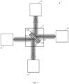
- FIG. 1 illustrates a first embodiment of a measurement system 1 according to the present disclosure for analysing RF signals.
- the measurement system 1 comprises an optically transparent enclosure 11 comprising an optically pumpable gas.
- the optically transparent enclosure 11 may comprise an optically transparent body or window made of optically transparent material such as borosilicate glass or aluminosciliate glass.
- the enclosure 11 may be a gas cell / atomic vapor cell.
- the gas may comprise an alkali metal, preferably Rubidium.
- Cesium may be used, or even non-alkali metals such as Helium.
- the measurement system 1 further comprises - without loss of generality - a PCB 12A comprising an electrical transmission line 121-123 for guiding the RF signal to be analyzed through the enclosure 11.
- the transmission line 121-123 may comprise an insulator layer 122 sandwiched between conductor layers 121, 123.
- the conductor 121 is configured to guide the RF signal to be analyzed through the enclosure 11, and any conductors 123 may relate to a ground potential. Responsive to RF signal propagation along the conductor 121, a non-radiative electromagnetic field emerges in a near-field region of the same.
- a magnetic portion thereof is illustrated in FIGs. 2 and 3 as closed field lines around the respective conductor 121, whereas field lines of an electric portion thereof (not shown) run perpendicularly to the field lines of the magnetic portion and terminate perpendicularly in the conductors 121, 123.
- the transmission line 121-123 may include one of: a microstrip (see FIG. 2 below), and a coplanar waveguide with ground (see FIG. 3 below).
- the emerging non-radiative electromagnetic field should be able to extend outside the PCB 12A, where the electromagnetic field of the RF signal may interact with the gas particles of the enclosure 11. More specifically, a respective absorption rate of frequency components of the RF signal increases with a respective energy of the frequency components. As such, for a given duration of the emerging non-radiative electromagnetic field, high-energy frequency components achieve a more exhaustive population inversion of the gas particles from the initial state/level to the excited state/level than low-energy frequency components, corresponding to intensity-dependent filtering.
- the PCB 12A further comprises a reflective planar face.
- the PCB 12A, 12B may include one of: a reflective coating 124; and a polished conductor layer 121, 123.
- the reflective coating 124 may comprise one of: a reflective dielectric coating comprising a quarterwave stack of alternating high and low index layers, and a reflective metal coating.
- a spectral width of the reflection band and the achievable reflectivity for a given number of layer pairs depends on the ratio of the refractive indices of the layer materials. For example, a large refractive index ratio yields a broad reflection band.
- reflective metallic coatings a surface of which may be oxidation-protected for maintaining a reflection property of the same.
- the reflective planar face of the PCB 12A may have a reflectance for the emitted light in excess of 80%. This may be achieved by reflective dielectric coatings based on a quarterwave stack comprising ⁇ 5 pairs of Ta 2 O 5 /SiO 2 in the reflection band 700-900nm. Similar results may be obtained using pairs of TiO 2 /SiO 2 layers. On the other hand, the reflective dielectric coatings should be made as thin as possible in order not to shield the emerging near field. A reflectancy in excess of 80% in the reflection band 700-900nm may also be achieved by reflective metallic surfaces, e.g., polished conductor layers 121, 123 made of one of: aluminum, copper, silver, and gold.
- reflective metallic surfaces e.g., polished conductor layers 121, 123 made of one of: aluminum, copper, silver, and gold.
- the measurement system 1 further comprises an optical pump 13 for emitting preferably coherent light onto the reflective planar face.
- an optical pump 13 for emitting preferably coherent light onto the reflective planar face.
- a laser source may be deployed for emitting coherent light.
- optical pumping and optical readout may realized by a single pump (as described in this implementation) or by separate pumps. In a setup with separate optical pumps, it would be beneficial if both beams overlap well with the electromagnetic field of the RF signal. If sensing is performed using Rydberg atoms, at least one more optical pump is needed for excitation to the Rydberg state.
- the optical pump 13 may be arranged to emit the light in a continuous wave, CW, mode or in a pulsed mode.
- the emitted light may have a wavelength in accordance with an energy transition of the gas, preferably 780 nm or 795 nm specifically for Rubidium, such that the atoms of the gas may be pumped from a ground energy state/level to highly excited initial energy states/levels wherein an outermost electron is substantially farther away from a nucleus as in the initial energy state/level.
- the initial energy state of a quantum system based on the atoms of the gas may comprise a Rydberg state.
- Rydberg states have multiple energy transitions in the GHz-THz range so that they are sensitive to excitation by magnetic fields, and particularly by electric fields, in a wide frequency range. Excitation to Rydberg state may be achieved using at least one further optical pump in addition to said 780/795 nm optical pumps.
- the optical pump 13 may be arranged to emit the light perpendicularly to a propagation direction of the RF signal.
- the RF signal to be analyzed propagates perpendicular to a drawing plane of FIG. 1 , whereas the emitted light propagates within the drawing plane.
- Propagation directions of the emitted light and the reflected light may form an intermediate angle 15 of at most 174°, preferably at most 160°, more preferably at most 140°, and most preferably 90°.
- directing a laser beam closely along, i.e., substantially parallel to, a surface as known in the art should be avoided.
- the measurement system 1 further comprises a detector 14 for detecting an optical property of the emitted light being reflected by the reflective planar face.
- the optical property may comprise an optical intensity or a photon count.
- the detector 14 may comprise one of: a photodiode for punctiform detection, and a camera for spatially resolved detection in accordance with an interaction of the emerging near field of the RF signal to be analyzed and the incident/reflected light beams having spatially resolved intensities (see an exemplary beam intensity profile indicated in FIG. 1 between the optical pump 13 and the enclosure 11).
- the spatially resolved optical pumping results in spatially resolved population of the initial energy state/level of the quantum system formed by the optically pumpable gas, and thus a spatially resolved (cap)ability of the quantum system to be ionized easily by absorption when exposed to external electro-magnetic RF fields.
- Such a (near) field may be induced around the electrical transmission line 121-123 when guiding an RF signal to be analyzed through the enclosure 11.
- the detector 14 and the optical pump 13 may be arranged non-coaxially in accordance with the intermediate angle 15.
- An intermediate angle of 90° may simplify the non-coaxial arrangement, whereas larger intermediate angles 15 of less than 180° may further improve a reflection property of the reflective planar face.
- only the beam for optical readout needs to be imaged/reflected to the optical detector.
- Presence of a magnetic or electric field may be used to cause splitting/shifts of the atomic energy levels in accordance with Zeeman or Stark splitting, which ensures availability of gas particles in an initial state for each frequency in a desired frequency range, such as an RF / microwave frequency range between 300 MHz and 300 GHz, respectively.
- a desired frequency range such as an RF / microwave frequency range between 300 MHz and 300 GHz, respectively.
- filtering may be possible up to the THz regime.
- Zeeman splitting may refer to splitting of a spectral line into several components in the presence of a static magnetic field.
- Stark splitting the electric-field analogue of Zeeman splitting, may refer to splitting of a spectral line into several components in the presence of a static electric field.
- FIGs. 2, 3 illustrate various embodiments of a PCB 12A, 12B according to the present disclosure for guiding RF signals to be analyzed through an enclosure 11 of the measurement system 1.
- the depicted PCBs 12A, 12B respectively comprise an electrical transmission line 121-123 for guiding the RF signal to be analyzed through the enclosure 11 of the measurement system 1.
- the respective transmission line 121-123 may comprise an insulator layer 122 sandwiched between conductor layers 121, 123.
- the respective transmission line 121-123 includes a microstrip in FIG. 2 , and a coplanar waveguide with ground in FIG. 3 .
- the respective PCB 12A, 12B comprises a reflective planar face in accordance with what has been set out above.
- FIG. 4 illustrates a second embodiment of a measurement system 1 according to the present disclosure for analysing RF signals.
- the PCB 12A, 12B may comprise two electrical transmission lines 121-123 on respective reflective planar faces of the PCB 12A, 12B.
- the PCB 12B comprises two coplanar waveguides with ground arranged back-to-back.
- this embodiment of the measurement system 1 may comprise two optical pumps 13 for emitting light in accordance with an energy transition of the gas, and two detectors 14 for detecting an optical property of the emitted light emitted by the respective optical pump 13 and reflected by the respective reflective planar face. This may reduce a space requirement of such a twin quantum sensor.
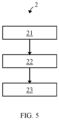
- FIG. 5 illustrates an embodiment of a method of operating the measurement systems 1 of FIGs. 1 and 2 .
- the measurement system 1 to be operated comprises a optically transparent enclosure 11 comprising an optically pumpable gas, a printed circuit board, PCB 12A, 12B comprising an electrical transmission line 121-123, an optical pump 13, and a detector 14.
- the PCB 12A, 12B further comprises a reflective planar face.
- the method 2 comprises guiding 21 the RF signal to be analyzed through the enclosure 11 via the transmission line 121-123.
- the method 2 comprises emitting 22 preferably coherent light onto the reflective planar face.
- the method 2 comprises detecting 23 an optical property of the emitted light being reflected by the planar face.
Description
- The present disclosure relates to signal analysis in microwave communication, and in particular to a measurement system for analysing RF signals and a method of operating the measurement system.
- Atom-based quantum effects may be used in developing quantum sensors for various physical quantities, as is known in the art.
- For example, in highly excited energy states/levels wherein an outermost electron is substantially farther away from a nucleus as in an initial energy state/level, atomic vapor may exhibit sensitive responses to external electromagnetic radio-frequency (RF) fields, ranging from several to hundreds of gigahertz (GHz). This coincides with a microwave frequency range between 300 MHz and 300 GHz, respectively.
- For quantum sensors of high sensitivity, it is crucial to overlap those sections with highest excitation (laser intensity) and microwave field strength.
- Conventionally, this involves directing a laser beam closely along a surface, which implies laborious laser beam alignment in combination with vulnerability to mechanical shocks and temperature changes. A relevant example of an RF measurement system comprising an optically pumpable gas is described in "Waveguide-coupled Rydberg spectrum analyzer from 0 to 20 GHz", DAVID H MEYER ET AL, Phys. Rev. Applied 15, 014053, January 2021.
- In view of the above-mentioned drawbacks and limitations, the present disclosure aims to improve RF signal analysis of the background art. An objective is to make RF signal analysis more sensitive, more robust and less burdensome.
- The objective is achieved by the embodiments as defined by the appended independent claims. Preferred embodiments are set forth in the dependent claims and in the following description and drawings.
- A first aspect of the present disclosure relates to a measurement system for analysing RF signals. The measurement system comprises a optically transparent enclosure comprising an optically pumpable gas, and a printed circuit board, PCB, comprising an electrical transmission line for guiding the RF signal to be analyzed through the enclosure and a reflective planar face. The measurement system further comprises an optical pump for emitting preferably coherent light onto the reflective planar face, and a detector for detecting an optical property of the emitted light being reflected by the reflective planar face.
- The gas may comprise an alkali metal, preferably Rubidium.
- The transmission line may comprise an insulator layer sandwiched between conductor layers.
- The transmission line may include one of: a microstrip, and a coplanar waveguide with ground.
- The transmission line may include one of: a reflective coating, and a polished conductor layer.
- The reflective coating may comprise one of: a reflective dielectric coating comprising a quarterwave stack of alternating high and low index layers, and a reflective metal coating.
- The reflective planar face of the PCB (12A, 12B) may have a reflectance for the emitted light in excess of 80%.
- The emitted light may have a wavelength in accordance with an energy transition of the gas, preferably 780 nm or 795 nm.
- The optical pump may be arranged to emit the light in a continuous wave, CW, mode or in a pulsed mode.
- The optical pump may be arranged to emit the light perpendicularly to a propagation direction of the RF signal.
- Propagation directions of the emitted light and the reflected light may form an intermediate angle of at most 174°, preferably at most 160°, more preferably at most 140°, and most preferably 90°.
- The detector and the optical pump may be arranged non-coaxially in accordance with the intermediate angle.
- The detector may comprise one of: a photodiode, and a camera.
- The PCB may comprise two electrical transmission lines on respective reflective planar faces of the PCB; and the measurement system may comprise two optical pumps for emitting light in accordance with an energy transition of the gas, and two detectors for detecting an optical property of the emitted light emitted by the respective optical pump and reflected by the respective reflective planar face.
- A second aspect of the present disclosure relates to a method of operating a measurement system for analysing RF signals. The measurement system comprises a optically transparent enclosure comprising an optically pumpable gas, a printed circuit board, PCB, comprising an electrical transmission line, an optical pump, and a detector. The PCB comprises a reflective planar face. The method comprises guiding the RF signal to be analyzed through the enclosure via the transmission line, emitting preferably coherent light onto the reflective planar face, and detecting an optical property of the emitted light being reflected by the reflective planar face.
- The present disclosure proposes using a surface of a PCB to reflect light / laser beams, coating and/or polishing the surface of the PCB to improve reflectivity, and choosing the right material for optimizing reflectivity for a particular wavelength.
- This provides a better laser/microwave overlap in atomic vapor quantum sensing setups, where it is crucial to overlap the regions with highest laser intensity and microwave field strength, and implies a higher sensitivity of atomic vapor quantum sensors, less effort for laser beam alignment, an improved robustness to mechanical shocks/temperature changes, and a possibility to use both sides of the PCB as reflective surfaces.
- Advantageously, the technical effects and advantages described above in relation with the measurement system equally apply to the method of operating the same having corresponding features.
- The above-described aspects and implementations will now be explained with reference to the accompanying drawings, in which the same or similar reference numerals designate the same or similar elements.
- The features of these aspects and implementations may be combined with each other unless specifically stated otherwise.
- The drawings are to be regarded as being schematic representations, and elements illustrated in the drawings are not necessarily shown to scale. Rather, the various elements are represented such that their function and general purpose become apparent to those skilled in the art.
- FIG. 1
- illustrates a first embodiment of a measurement system according to the present disclosure for analysing RF signals;
- FIGs. 2, 3
- illustrate various embodiments of a PCB according to the present disclosure for guiding RF signals to be analyzed through an enclosure of the measurement system;
- FIG. 4
- illustrates a second embodiment of a measurement system according to the present disclosure for analysing RF signals; and
- FIG. 5
- illustrates an embodiment of a method of operating the measurement systems of
FIGs. 1 and 2 . -
FIG. 1 illustrates a first embodiment of ameasurement system 1 according to the present disclosure for analysing RF signals. - The
measurement system 1 comprises an opticallytransparent enclosure 11 comprising an optically pumpable gas. In particular, the opticallytransparent enclosure 11 may comprise an optically transparent body or window made of optically transparent material such as borosilicate glass or aluminosciliate glass. For example, theenclosure 11 may be a gas cell / atomic vapor cell. - The gas may comprise an alkali metal, preferably Rubidium. Alternatively, Cesium may be used, or even non-alkali metals such as Helium.
- The
measurement system 1 further comprises - without loss of generality - aPCB 12A comprising an electrical transmission line 121-123 for guiding the RF signal to be analyzed through theenclosure 11. - The transmission line 121-123 may comprise an
insulator layer 122 sandwiched betweenconductor layers conductor 121 is configured to guide the RF signal to be analyzed through theenclosure 11, and anyconductors 123 may relate to a ground potential. Responsive to RF signal propagation along theconductor 121, a non-radiative electromagnetic field emerges in a near-field region of the same. A magnetic portion thereof is illustrated inFIGs. 2 and 3 as closed field lines around therespective conductor 121, whereas field lines of an electric portion thereof (not shown) run perpendicularly to the field lines of the magnetic portion and terminate perpendicularly in theconductors - In particular, the transmission line 121-123 may include one of: a microstrip (see
FIG. 2 below), and a coplanar waveguide with ground (seeFIG. 3 below). Key point is that the emerging non-radiative electromagnetic field should be able to extend outside thePCB 12A, where the electromagnetic field of the RF signal may interact with the gas particles of theenclosure 11. More specifically, a respective absorption rate of frequency components of the RF signal increases with a respective energy of the frequency components. As such, for a given duration of the emerging non-radiative electromagnetic field, high-energy frequency components achieve a more exhaustive population inversion of the gas particles from the initial state/level to the excited state/level than low-energy frequency components, corresponding to intensity-dependent filtering. - The
PCB 12A further comprises a reflective planar face. In particular, thePCB reflective coating 124; and apolished conductor layer - The
reflective coating 124 may comprise one of: a reflective dielectric coating comprising a quarterwave stack of alternating high and low index layers, and a reflective metal coating. - As for reflective dielectric coatings, the so-called quarterwave stack, i.e., a stack of alternating high and low index layers with an optical thickness of n·t = λ/4 for the desired wavelength λ (where n and t relate to a refractive index and a geometrical thickness of the respective layer) achieves constructive interference of the reflected beams arising at each interface between the layers. A spectral width of the reflection band and the achievable reflectivity for a given number of layer pairs depends on the ratio of the refractive indices of the layer materials. For example, a large refractive index ratio yields a broad reflection band.
- As for reflective metallic coatings, a surface of which may be oxidation-protected for maintaining a reflection property of the same.
- The reflective planar face of the
PCB 12A may have a reflectance for the emitted light in excess of 80%. This may be achieved by reflective dielectric coatings based on a quarterwave stack comprising ≥5 pairs of Ta2O5/SiO2 in the reflection band 700-900nm. Similar results may be obtained using pairs of TiO2/SiO2 layers. On the other hand, the reflective dielectric coatings should be made as thin as possible in order not to shield the emerging near field. A reflectancy in excess of 80% in the reflection band 700-900nm may also be achieved by reflective metallic surfaces, e.g., polished conductor layers 121, 123 made of one of: aluminum, copper, silver, and gold. - The
measurement system 1 further comprises anoptical pump 13 for emitting preferably coherent light onto the reflective planar face. In particular, a laser source may be deployed for emitting coherent light. - Depending on the implementation, optical pumping and optical readout may realized by a single pump (as described in this implementation) or by separate pumps. In a setup with separate optical pumps, it would be beneficial if both beams overlap well with the electromagnetic field of the RF signal. If sensing is performed using Rydberg atoms, at least one more optical pump is needed for excitation to the Rydberg state.
- The
optical pump 13 may be arranged to emit the light in a continuous wave, CW, mode or in a pulsed mode. The emitted light may have a wavelength in accordance with an energy transition of the gas, preferably 780 nm or 795 nm specifically for Rubidium, such that the atoms of the gas may be pumped from a ground energy state/level to highly excited initial energy states/levels wherein an outermost electron is substantially farther away from a nucleus as in the initial energy state/level. For example, the initial energy state of a quantum system based on the atoms of the gas may comprise a Rydberg state. Rydberg states have multiple energy transitions in the GHz-THz range so that they are sensitive to excitation by magnetic fields, and particularly by electric fields, in a wide frequency range. Excitation to Rydberg state may be achieved using at least one further optical pump in addition to said 780/795 nm optical pumps. - The
optical pump 13 may be arranged to emit the light perpendicularly to a propagation direction of the RF signal. In the implementation ofFIG. 1 , the RF signal to be analyzed propagates perpendicular to a drawing plane ofFIG. 1 , whereas the emitted light propagates within the drawing plane. - Propagation directions of the emitted light and the reflected light may form an
intermediate angle 15 of at most 174°, preferably at most 160°, more preferably at most 140°, and most preferably 90°. In other words, directing a laser beam closely along, i.e., substantially parallel to, a surface as known in the art should be avoided. - The
measurement system 1 further comprises adetector 14 for detecting an optical property of the emitted light being reflected by the reflective planar face. For example, the optical property may comprise an optical intensity or a photon count. - The
detector 14 may comprise one of: a photodiode for punctiform detection, and a camera for spatially resolved detection in accordance with an interaction of the emerging near field of the RF signal to be analyzed and the incident/reflected light beams having spatially resolved intensities (see an exemplary beam intensity profile indicated inFIG. 1 between theoptical pump 13 and the enclosure 11). The spatially resolved optical pumping results in spatially resolved population of the initial energy state/level of the quantum system formed by the optically pumpable gas, and thus a spatially resolved (cap)ability of the quantum system to be ionized easily by absorption when exposed to external electro-magnetic RF fields. Such a (near) field may be induced around the electrical transmission line 121-123 when guiding an RF signal to be analyzed through theenclosure 11. - The
detector 14 and theoptical pump 13 may be arranged non-coaxially in accordance with theintermediate angle 15. An intermediate angle of 90° may simplify the non-coaxial arrangement, whereas largerintermediate angles 15 of less than 180° may further improve a reflection property of the reflective planar face. In a setup with separate optical pumps, only the beam for optical readout needs to be imaged/reflected to the optical detector. - Presence of a magnetic or electric field may be used to cause splitting/shifts of the atomic energy levels in accordance with Zeeman or Stark splitting, which ensures availability of gas particles in an initial state for each frequency in a desired frequency range, such as an RF / microwave frequency range between 300 MHz and 300 GHz, respectively. For particles in the Rydberg state, filtering may be possible up to the THz regime. For initial-state Rubidium atoms in a magnetic field, filtering may be possible up to ~60 GHz.
- Zeeman splitting may refer to splitting of a spectral line into several components in the presence of a static magnetic field. Stark splitting, the electric-field analogue of Zeeman splitting, may refer to splitting of a spectral line into several components in the presence of a static electric field.
-
FIGs. 2, 3 illustrate various embodiments of aPCB enclosure 11 of themeasurement system 1. - The depicted
PCBs enclosure 11 of themeasurement system 1. - The respective transmission line 121-123 may comprise an
insulator layer 122 sandwiched between conductor layers 121, 123. - The respective transmission line 121-123 includes a microstrip in
FIG. 2 , and a coplanar waveguide with ground inFIG. 3 . - The
respective PCB -
FIG. 4 illustrates a second embodiment of ameasurement system 1 according to the present disclosure for analysing RF signals. - As may be taken from
FIG. 4 , in this embodiment of themeasurement system 1 thePCB PCB FIG. 4 , thePCB 12B comprises two coplanar waveguides with ground arranged back-to-back. - Likewise, this embodiment of the
measurement system 1 may comprise twooptical pumps 13 for emitting light in accordance with an energy transition of the gas, and twodetectors 14 for detecting an optical property of the emitted light emitted by the respectiveoptical pump 13 and reflected by the respective reflective planar face. This may reduce a space requirement of such a twin quantum sensor. -
FIG. 5 illustrates an embodiment of a method of operating themeasurement systems 1 ofFIGs. 1 and 2 . - The
measurement system 1 to be operated comprises a opticallytransparent enclosure 11 comprising an optically pumpable gas, a printed circuit board,PCB optical pump 13, and adetector 14. ThePCB - In a first step, the method 2 comprises guiding 21 the RF signal to be analyzed through the
enclosure 11 via the transmission line 121-123. - In a second step, the method 2 comprises emitting 22 preferably coherent light onto the reflective planar face.
- In a third step, the method 2 comprises detecting 23 an optical property of the emitted light being reflected by the planar face.
Claims (15)
- A measurement system (1) for analysing RF signals, comprisinga optically transparent enclosure (11) comprising an optically pumpable gas;a printed circuit board, PCB (12A, 12B), comprising an electrical transmission line (121-123) for guiding the RF signal to be analyzed through the enclosure (11) and a reflective planar face;an optical pump (13) for emitting preferably coherent light onto the reflective planar face; and a detector (14) for detecting an optical property of the emitted light being reflected by the reflective planar face.
- The measurement system (1) of claim 1,
the gas comprising an alkali metal, preferably Rubidium. - The measurement system (1) of any one of the preceding claims,
the transmission line (121-123) comprising an insulator layer (122) sandwiched between conductor layers (121, 123). - The measurement system (1) of claim 3,
the transmission line (121-123) including one of:- a microstrip; and- a coplanar waveguide with ground. - The measurement system (1) of any one of the preceding claims,
the PCB (12A, 12B) including one of:- a reflective coating (124); and- a polished conductor layer (121, 123). - The measurement system (1) of claim 5,
the reflective coating (124) comprising one of:- a reflective dielectric coating comprising a quarterwave stack of alternating high and low index layers; and- a reflective metal coating. - The measurement system (1) of any one of the preceding claims,
the reflective planar face of the PCB (12A, 12B) having a reflectance for the emitted light in excess of 80%. - The measurement system (1) of any one of the preceding claims,
the emitted light having a wavelength in accordance with an energy transition of the gas, preferably 780 nm or 795 nm. - The measurement system (1) of any one of the preceding claims,
the optical pump (13) arranged to emit the light in a continuous wave, CW, mode or in a pulsed mode. - The measurement system (1) of any one of the preceding claims,
the optical pump (13) arranged to emit the light perpendicularly to a propagation direction of the RF signal. - The measurement system (1) of any one of the preceding claims,
propagation directions of the emitted light and the reflected light forming an intermediate angle (15) of at most 174°, preferably at most 160°, more preferably at most 140°, and most preferably 90°. - The measurement system (1) of claim 11,
the detector (14) and the optical pump (13) arranged non-coaxially in accordance with the intermediate angle (15). - The measurement system (1) of any one of the preceding claims,
the detector (14) comprising one of:- a photodiode; and- a camera. - The measurement system (1) of any one of the preceding claims,the PCB (12A, 12B) comprising two electrical transmission lines (121-123) on respective reflective planar faces of the PCB (12A, 12B); andthe measurement system (1) comprising- two optical pumps (13) for emitting light in accordance with an energy transition of the gas; and- two detectors (14) for detecting an optical property of the emitted light emitted by the respective optical pump (13) and reflected by the respective reflective planar face.
- A method (2) of operating a measurement system (1) for analysing RF signals,the measurement system (1) comprisinga optically transparent enclosure (11) comprising an optically pumpable gas;a printed circuit board, PCB (12A, 12B), comprising an electrical transmission line (121-123) and a reflective planar face;an optical pump (13); anda detector (14);the method (2) comprisingguiding (21) the RF signal to be analyzed through the enclosure (11) via the transmission line (121-123);emitting (22) preferably coherent light onto the reflective planar face; anddetecting (23) an optical property of the emitted light being reflected by the reflective planar face.
Priority Applications (2)
| Application Number | Priority Date | Filing Date | Title |
|---|---|---|---|
| EP21204629.6A EP4174498B8 (en) | 2021-10-26 | 2021-10-26 | Measurement system for analysing radio frequency signals, and method of operating the same |
| US17/949,774 US20230126884A1 (en) | 2021-10-26 | 2022-09-21 | Measurement system for analysing radio frequency signals, and method of operating the same |
Applications Claiming Priority (1)
| Application Number | Priority Date | Filing Date | Title |
|---|---|---|---|
| EP21204629.6A EP4174498B8 (en) | 2021-10-26 | 2021-10-26 | Measurement system for analysing radio frequency signals, and method of operating the same |
Publications (3)
| Publication Number | Publication Date |
|---|---|
| EP4174498A1 EP4174498A1 (en) | 2023-05-03 |
| EP4174498B1 true EP4174498B1 (en) | 2023-10-04 |
| EP4174498B8 EP4174498B8 (en) | 2023-11-15 |
Family
ID=78695453
Family Applications (1)
| Application Number | Title | Priority Date | Filing Date |
|---|---|---|---|
| EP21204629.6A Active EP4174498B8 (en) | 2021-10-26 | 2021-10-26 | Measurement system for analysing radio frequency signals, and method of operating the same |
Country Status (2)
| Country | Link |
|---|---|
| US (1) | US20230126884A1 (en) |
| EP (1) | EP4174498B8 (en) |
Families Citing this family (1)
| Publication number | Priority date | Publication date | Assignee | Title |
|---|---|---|---|---|
| EP4184184B8 (en) * | 2021-11-19 | 2023-11-15 | Rohde & Schwarz GmbH & Co. KG | Measurement system and method for analyzing rf signals |
Family Cites Families (3)
| Publication number | Priority date | Publication date | Assignee | Title |
|---|---|---|---|---|
| JP7034485B2 (en) * | 2018-09-28 | 2022-03-14 | 国立研究開発法人産業技術総合研究所 | Electromagnetic wave measuring device |
| EP3906418B1 (en) * | 2018-12-31 | 2023-03-01 | Quantum Valley Ideas Laboratories | Imaging of electromagnetic fields |
| US11435386B2 (en) * | 2019-03-15 | 2022-09-06 | Government Of The United States Of America, As Represented By The Secretary Of Commerce | Si-traceable Rydberg atom radiofrequency power meter and determining power of radio frequency radiation |
-
2021
- 2021-10-26 EP EP21204629.6A patent/EP4174498B8/en active Active
-
2022
- 2022-09-21 US US17/949,774 patent/US20230126884A1/en active Pending
Also Published As
| Publication number | Publication date |
|---|---|
| US20230126884A1 (en) | 2023-04-27 |
| EP4174498B8 (en) | 2023-11-15 |
| EP4174498A1 (en) | 2023-05-03 |
Similar Documents
| Publication | Publication Date | Title |
|---|---|---|
| Yang et al. | Resonant transmission of microwaves through a narrow metallic slit | |
| Garcia-Vidal et al. | Transmission and focusing of light in one-dimensional periodically nanostructured metals | |
| Miyazaki et al. | Squeezing visible light waves into a 3-nm-thick and 55-nm-long plasmon cavity | |
| US7688274B2 (en) | Integrated filter in antenna-based detector | |
| US20090009190A1 (en) | Inspection Apparatus Using Terahertz Wave | |
| US20230126884A1 (en) | Measurement system for analysing radio frequency signals, and method of operating the same | |
| KR101467241B1 (en) | Surface plasmon polariton circuit element with discontinuous waveguide with gap and apparatus and method for generating surface plasmon polariton mode | |
| EP1926982B1 (en) | Waveguide, and device and detection method using the same | |
| US5850140A (en) | Electric field sensor having sensor head with unbalanced electric field shield to shield branched optical waveguides against an applied electric field | |
| Edelmann et al. | Coupling of terahertz radiation to metallic wire using end‐fire technique | |
| US9335478B2 (en) | Suppression of back reflection in a waveguide | |
| US5012212A (en) | Open resonator for electromagnetic waves having a polarized coupling region | |
| KR101129223B1 (en) | All optical logic device and optical modulator using surface plasmon resonance | |
| Sun et al. | Plasmonic Polarization‐Rotating Emitters with Metallic Nanogroove Antennas | |
| US20070177150A1 (en) | Surface plasmon resonance biosensor using coupled surface plasmons to decrease width of reflectivity dip | |
| Kawalec et al. | Spectroscopic measurements of the evanescent wave polarization state | |
| Glushko | Induced resonant electromagnetic piercing in metalized photonic crystal structures | |
| Haque et al. | Graphene based surface plasmon resonance (SPR) sensors: An approach to enhance the performance | |
| Zhang et al. | Graphene based surface plasmon resonance gas sensor with magnetic field control for terahertz | |
| Liu et al. | Tunable Fano resonances and improved sensitivity in waveguide-coupled surface plasmon resonance sensors with a bimetallic layer | |
| Imai et al. | Scattering pattern measurement and analysis of sputtered-glass optical waveguides for integrated optics | |
| KR101557229B1 (en) | Surface plasmon polariton logic circuit elements capable of various logic operations and method for logic operation thereof | |
| Yakovlev et al. | Waveguide modes as a sensitive probe of superthin surface metal films | |
| Divitt et al. | Cylindrical, High-Q Surface Plasmon Cavities for Lasing and Sensing in the Visible Range | |
| CN109443704B (en) | Phase-enhanced optical intensity detection method and system |
Legal Events
| Date | Code | Title | Description |
|---|---|---|---|
| PUAI | Public reference made under article 153(3) epc to a published international application that has entered the european phase |
Free format text: ORIGINAL CODE: 0009012 |
|
| STAA | Information on the status of an ep patent application or granted ep patent |
Free format text: STATUS: REQUEST FOR EXAMINATION WAS MADE |
|
| 17P | Request for examination filed |
Effective date: 20220607 |
|
| AK | Designated contracting states |
Kind code of ref document: A1 Designated state(s): AL AT BE BG CH CY CZ DE DK EE ES FI FR GB GR HR HU IE IS IT LI LT LU LV MC MK MT NL NO PL PT RO RS SE SI SK SM TR |
|
| P01 | Opt-out of the competence of the unified patent court (upc) registered |
Effective date: 20230525 |
|
| GRAP | Despatch of communication of intention to grant a patent |
Free format text: ORIGINAL CODE: EPIDOSNIGR1 |
|
| STAA | Information on the status of an ep patent application or granted ep patent |
Free format text: STATUS: GRANT OF PATENT IS INTENDED |
|
| GRAS | Grant fee paid |
Free format text: ORIGINAL CODE: EPIDOSNIGR3 |
|
| INTG | Intention to grant announced |
Effective date: 20230718 |
|
| GRAA | (expected) grant |
Free format text: ORIGINAL CODE: 0009210 |
|
| STAA | Information on the status of an ep patent application or granted ep patent |
Free format text: STATUS: THE PATENT HAS BEEN GRANTED |
|
| AK | Designated contracting states |
Kind code of ref document: B1 Designated state(s): AL AT BE BG CH CY CZ DE DK EE ES FI FR GB GR HR HU IE IS IT LI LT LU LV MC MK MT NL NO PL PT RO RS SE SI SK SM TR |
|
| REG | Reference to a national code |
Ref country code: GB Ref legal event code: FG4D |
|
| REG | Reference to a national code |
Ref country code: CH Ref legal event code: PLX Ref country code: CH Ref legal event code: EP |
|
| REG | Reference to a national code |
Ref country code: DE Ref legal event code: R096 Ref document number: 602021005611 Country of ref document: DE |
|
| REG | Reference to a national code |
Ref country code: IE Ref legal event code: FG4D |
|
| RBV | Designated contracting states (corrected) |
Designated state(s): AL AT BE BG CY CZ DE DK EE ES FI FR GB GR HR HU IS IT LT LU LV MC MK MT NL NO PL PT RO RS SE SI SK SM TR |
|
| REG | Reference to a national code |
Ref country code: LT Ref legal event code: MG9D |
|
| PGFP | Annual fee paid to national office [announced via postgrant information from national office to epo] |
Ref country code: FR Payment date: 20231121 Year of fee payment: 3 Ref country code: DE Payment date: 20231127 Year of fee payment: 3 |
|
| REG | Reference to a national code |
Ref country code: NL Ref legal event code: MP Effective date: 20231004 |
|
| REG | Reference to a national code |
Ref country code: AT Ref legal event code: MK05 Ref document number: 1618258 Country of ref document: AT Kind code of ref document: T Effective date: 20231004 |
|
| PG25 | Lapsed in a contracting state [announced via postgrant information from national office to epo] |
Ref country code: NL Free format text: LAPSE BECAUSE OF FAILURE TO SUBMIT A TRANSLATION OF THE DESCRIPTION OR TO PAY THE FEE WITHIN THE PRESCRIBED TIME-LIMIT Effective date: 20231004 |
|
| PG25 | Lapsed in a contracting state [announced via postgrant information from national office to epo] |
Ref country code: GR Free format text: LAPSE BECAUSE OF FAILURE TO SUBMIT A TRANSLATION OF THE DESCRIPTION OR TO PAY THE FEE WITHIN THE PRESCRIBED TIME-LIMIT Effective date: 20240105 |
|
| PG25 | Lapsed in a contracting state [announced via postgrant information from national office to epo] |
Ref country code: IS Free format text: LAPSE BECAUSE OF FAILURE TO SUBMIT A TRANSLATION OF THE DESCRIPTION OR TO PAY THE FEE WITHIN THE PRESCRIBED TIME-LIMIT Effective date: 20240204 |
|
| PG25 | Lapsed in a contracting state [announced via postgrant information from national office to epo] |
Ref country code: LT Free format text: LAPSE BECAUSE OF FAILURE TO SUBMIT A TRANSLATION OF THE DESCRIPTION OR TO PAY THE FEE WITHIN THE PRESCRIBED TIME-LIMIT Effective date: 20231004 |
|
| PG25 | Lapsed in a contracting state [announced via postgrant information from national office to epo] |
Ref country code: AT Free format text: LAPSE BECAUSE OF FAILURE TO SUBMIT A TRANSLATION OF THE DESCRIPTION OR TO PAY THE FEE WITHIN THE PRESCRIBED TIME-LIMIT Effective date: 20231004 |