EP4170655A1 - Sram mit rekonfigurierbarer initialisierung - Google Patents
Sram mit rekonfigurierbarer initialisierung Download PDFInfo
- Publication number
- EP4170655A1 EP4170655A1 EP22198595.5A EP22198595A EP4170655A1 EP 4170655 A1 EP4170655 A1 EP 4170655A1 EP 22198595 A EP22198595 A EP 22198595A EP 4170655 A1 EP4170655 A1 EP 4170655A1
- Authority
- EP
- European Patent Office
- Prior art keywords
- initialization
- line
- bit line
- bias
- erase
- Prior art date
- Legal status (The legal status is an assumption and is not a legal conclusion. Google has not performed a legal analysis and makes no representation as to the accuracy of the status listed.)
- Pending
Links
Images



Classifications
-
- G—PHYSICS
- G11—INFORMATION STORAGE
- G11C—STATIC STORES
- G11C7/00—Arrangements for writing information into, or reading information out from, a digital store
- G11C7/20—Memory cell initialisation circuits, e.g. when powering up or down, memory clear, latent image memory
-
- G—PHYSICS
- G11—INFORMATION STORAGE
- G11C—STATIC STORES
- G11C11/00—Digital stores characterised by the use of particular electric or magnetic storage elements; Storage elements therefor
- G11C11/21—Digital stores characterised by the use of particular electric or magnetic storage elements; Storage elements therefor using electric elements
- G11C11/34—Digital stores characterised by the use of particular electric or magnetic storage elements; Storage elements therefor using electric elements using semiconductor devices
- G11C11/40—Digital stores characterised by the use of particular electric or magnetic storage elements; Storage elements therefor using electric elements using semiconductor devices using transistors
- G11C11/41—Digital stores characterised by the use of particular electric or magnetic storage elements; Storage elements therefor using electric elements using semiconductor devices using transistors forming static cells with positive feedback, i.e. cells not needing refreshing or charge regeneration, e.g. bistable multivibrator or Schmitt trigger
- G11C11/413—Auxiliary circuits, e.g. for addressing, decoding, driving, writing, sensing, timing or power reduction
- G11C11/417—Auxiliary circuits, e.g. for addressing, decoding, driving, writing, sensing, timing or power reduction for memory cells of the field-effect type
- G11C11/419—Read-write [R-W] circuits
-
- G—PHYSICS
- G11—INFORMATION STORAGE
- G11C—STATIC STORES
- G11C5/00—Details of stores covered by group G11C11/00
- G11C5/14—Power supply arrangements, e.g. power down, chip selection or deselection, layout of wirings or power grids, or multiple supply levels
- G11C5/148—Details of power up or power down circuits, standby circuits or recovery circuits
-
- G—PHYSICS
- G11—INFORMATION STORAGE
- G11C—STATIC STORES
- G11C7/00—Arrangements for writing information into, or reading information out from, a digital store
- G11C7/24—Memory cell safety or protection circuits, e.g. arrangements for preventing inadvertent reading or writing; Status cells; Test cells
Definitions
- the present invention relates to the field of memories, and in particular of the SRAM type (SRAM for "Static Random Access Memory” or static random access memory), and relates more specifically to that of the initialization of SRAM memories, in particular when this initialization serves as a countermeasure to prevent fraudulent access.
- SRAM Static Random Access Memory
- the present invention implements an improved initialization circuit making it possible to perform different types of initialization.
- An SRAM memory has the function of storing volatile information, some of which, for example such as encryption keys, may be confidential and/or need to be secured. There are a reduced number of techniques for initializing an SRAM memory.
- the most well-known initialization technique is a so-called “free” initialization, which consists in the ignition without constraints of a plan of memory cells.
- free initialization the state in which each cell is initialized is set freely.
- the cell of the i -th column and the j -th row has a probability p ijk to initialize to a logical level '1' and a 1-p probability ijk to initialize to a logical level '0'.
- the initialization state of the memory or of certain cells of the memory is thus capable of constituting a fingerprint or digital signature.
- these are in particular cells with a high probability of switching and initializing at a given logic level ( p ijk equal to or very close to 1 for cells with a strong tendency to initialize at '1' and p ijk equal to or very close to 0 for cells with a strong tendency to initialize to '0') which can be used to form this digital fingerprint of the k-th chip.
- the initialization of a memory which is in operation requires a preliminary erasing step. It can consist in, initially, cutting off the memory supply in particular either by bringing it to ground or by placing it at a negative voltage until its contents are completely erased, then, in supplying memory again.
- FIG. 1A thus illustrates an erasing technique that can be implemented to perform a free initialization.
- a memory circuit 10 formed of SRAM cells and which is powered by a supply voltage VDD is brought to a reference potential GND, by switching a switch element 12.
- a disadvantage of free initialization is that in the event of malicious intrusion after such initialization, a third-party device may possibly recover this fingerprint or digital signature.
- FIG. 1B Another erase technique that can be used to initialize a memory is illustrated in figure 1B and consists in connecting the internal nodes NT, NF of an SRAM cell after having previously disconnected it from its power source.
- This technique here requires the addition of a transistor T 1 at the level of the memory cell which alternately makes it possible to connect or disconnect the internal nodes NT, NF from one another depending on the state of a reset signal RESET .
- Setting Implementing this type of erasure requires a modification of the structure of the cells which is moreover to the detriment of the integration density.
- a so-called “deterministic” initialization technique consists of writing, address after address, a predetermined content which may have been fixed beforehand by the user or the designer of the memory.
- a write operation driver circuit 20 can be configured to perform a deterministic initialization, in which the state of each memory cell is forced to a determined value, for example by writing only '0' values or only '1' values in each memory cell.
- the implementation of this type of initialization is done here to the detriment of the time spent rewriting a certain number of memory points at different addresses, to the detriment of the associated consumption as well as to the risk of an information leak linked to this rewrite or carried out in a malicious way during this long operation.
- a single notation can be used for the two types of initialization, if it is considered that each cell is initialized during ignition, therefore during a rise ramp of the supply voltage VDD.
- the value p ijk therefore does not depend on the final value of the supply voltage, but rather on the speed of this voltage rise, which can be indicated through the slew rate V SR ( slew-rate, expressed in Volt /second).
- V SR slew-rate, expressed in Volt /second.
- the present application aims to find a new type of circuit for initializing the data contained in an SRAM which is improved with respect to the drawbacks mentioned above.
- the initialization circuit makes it possible, during the pre-initialization phase, to perform an erasure of data stored in the SRAM by equalizing the internal nodes of the memory cells and then to be able to initialize its content either according to a first initialization mode or either according to a second initialization mode.
- the first initialization mode can be a so-called “deterministic” initialization mode in which a logic value is imposed on each of the cells.
- the second initialization mode can be a so-called "free" initialization mode in which each cell is allowed to switch freely towards a logical value with a probability p ijk which follows a statistic p(P, V SR, 0, T) function local variations and operating conditions specific to this cell and the chip to which it belongs.
- An initialization circuit as implemented according to the invention thus gives the possibility of combining at least two initialization techniques in the same memory circuit.
- the first initialization mode may be a so-called “deterministic” initialization mode used for example when fraudulent access to the memory is detected.
- the first initialization mode can be used.
- the initialization circuit being further provided with: a switch element, in particular a transistor, configured to alternately connect to each other and disconnect from each other the first bit line and the second line bit, said switch element being controlled by a first control signal, so as to disconnecting the first bit line and the second bit line from each other during said second phase of the first initialization mode and the second initialization mode.
- a switch element in particular a transistor, configured to alternately connect to each other and disconnect from each other the first bit line and the second line bit, said switch element being controlled by a first control signal, so as to disconnecting the first bit line and the second bit line from each other during said second phase of the first initialization mode and the second initialization mode.
- the initialization circuit is further provided with another switch element, in particular another transistor, configured to alternately decouple the so-called "high" power supply line from a power supply during the initialization phase and to couple the "high" supply line and said supply during the second phase, the other switch element being controlled by said first control signal.
- another switch element in particular another transistor, configured to alternately decouple the so-called "high” power supply line from a power supply during the initialization phase and to couple the "high" supply line and said supply during the second phase, the other switch element being controlled by said first control signal.
- the matrix is further arranged in rows of one or more SRAM cells and in which a plurality of word lines are respectively connected to said plurality of SRAM memory cells of said column, each word line allowing , when activated, to select the memory cell(s) of a given row of SRAM cells from among said rows of SRAM cells, the initialization circuit further comprising a stage for simultaneously activating said word lines for, when of the second phase of said first initialization mode, carrying out, by means of a second control signal, maintaining simultaneous activation of said word lines of said group of cells.
- one of said first bit line and second bit line is brought to the supply potential while the other of said first bit line and second bit line is left floating or grounded or at a potential lower than the reference potential serving as ground.
- the first bias line and the second bias line are brought to the supply potential.
- the first coupling transistor has a size W1/L1 and the second coupling transistor has a size W2/L2 different from that of the first coupling transistor and/or at least one of said first potential polarization and second polarization potential is provided at a value ⁇ V such that: GND ⁇ V ⁇ VDD and in particular such that GND ⁇ V ⁇ VDD/10.
- the initialization circuit is provided with a logic control block able to receive a first trigger signal from the first initialization mode and a trigger signal from the second initialization mode and to produce consecutively to the reception of the first trigger signal a first sequence of control signals, putting the initialization circuit in the first initialization mode and to produce consecutively to the reception of the second trigger signal, a second sequence of said control signals , distinct from the first sequence and putting the initialization circuit in the second initialization mode.
- the logic control block can be provided with a first multiplexer and a second multiplexer, respectively producing the first control signal and the second control signal, a first input of the first multiplexer being connected to a second input of the second multiplexer and receiving an erase signal whose state depends on the first trigger signal and on the second trigger signal, a second input of the first multiplexer being connected to a first input of the second multiplexer, and receiving the erase signal with a predetermined delay, the second trigger signal forming a selection signal common to the first multiplexer and to the second multiplexer.
- a change of state of the second trigger signal follows detection of fraudulent access to the memory device.
- a change of state of the first trigger signal is consecutive to an emission of a signal coming from a module configured to generate a digital signature and/or an encryption key and/or a random number.
- the "high" supply line is decoupled from a supply at the supply potential VDD, so as not to supply the first inverter and the second inverter, and wherein during the second phase of the first mode and the second initialization mode, the "high" supply line is coupled to a supply at the supply potential VDD, so as to supply the first inverter and the second inverter .
- the present invention also relates to the use of a device as defined above to generate a digital signature and/or an encryption key and/or a random number.
- An initialization circuit as implemented according to the invention is integrated into an SRAM memory device comprising a memory plane M 1 formed of at least one column of cells.
- this memory plane M 1 is, as illustrated in the picture 3 , having a plurality of rows and columns of SRAM cells.
- the cells can have a conventional layout, which implies that the initialization circuit can be implemented without a modification of their internal structure being necessary.
- a conventional SRAM cell C ij is thus represented with its two storage nodes NT and NF, provided to keep a first logical information, and a logical information complementary to the first information. Maintaining the logic information in the nodes is ensured by transistors forming inverters INV1, INV2 looped on themselves.
- the two inverters INV1, INV2 are typically made by two load transistors and two driver transistors.
- the inverters INV1, INV2 are connected to a first power supply line, in particular a so-called “high” power supply line VirVDD, and to a second power supply line LGND, in particular a so-called “low” power supply line.
- the high supply line VirVDD is set to a potential, for example VDD, which is greater than that of the low feeder line LGND.
- Access to storage nodes NT and NF is achieved by means of two access transistors TA T and TA F connected respectively to bit lines BL T and BL F generally shared by the SRAM cells of the same column of matrix plan cells.
- This access to the storage nodes NT and NF is controlled by a word line WL generally shared by the SRAM cells of the same line of cells of the matrix plane.
- the access transistors TA T and TA F are thus provided to allow, when they are activated to allow access to the first node NT and to the second node NF, or when they are deactivated to block access to the first node NT and the second NF node.
- an initialization circuit 100 arranged on the periphery of the matrix plane M 1 .
- the initialization circuit 100 here only requires the implementation of a limited number of additional elements peripheral to the memory plane M 1 .
- the initialization circuit 100 has the particularity of being able to adopt different operating modes corresponding to different ways of initializing a group of memory cells or all of the cells of the memory array M 1 .
- a first operating mode makes it possible to carry out a deterministic initialization INIT_D. For this, at least one group of cells of the memory is written by imposing on each cell of this group a predetermined value '1' or '0'. A predetermined set of predetermined values is thus imposed on the group of cells that are initialized or reinitialized.
- a particular way of initializing according to the deterministic initialization mode is to impose the same state, for example '1' or '0', on all the cells of the group of initialized cells. Taking as convention that the value of the NT node of a cell is equal to the value memorized by this cell, this amounts here to writing a value 1' or '0' on the first respective NT nodes of the initialized group of cells.
- the deterministic initialization with a value imposed on each cell is then typically carried out simultaneously between the cells of a group of initialized cells.
- Means for simultaneous activation of the word lines for effecting a simultaneous activation of the word lines WL so as to effect a simultaneous selection of lines of SRAM cells are in this case provided.
- the predetermined value at which each initialized cell is placed can be fixed by the user of the memory or else by the designer of the memory.
- a particular embodiment illustrated in the picture 3 provides that the initialization circuit 100 is configured to perform deterministic initialization as a self-protection mechanism, for example to prevent malicious manipulation of the memory. It is thus possible to prevent a third-party device from accessing or damaging information from the memory device, and in particular memory identification or authentication data relating to the PUF (“Physically Unclonable Function”) serving as a digital signature or digital fingerprint of the memory. This prevents this digital fingerprint, which can for example be used to constitute an encryption key, from being obtained by the third-party device at the origin of the malicious manipulation.
- PUF Physical Unclonable Function
- a fraudulent access detection module 110 can be provided to transmit to the initialization circuit 100 a fraudulent access detection signal S AF making it possible to trigger its passage into a deterministic initialization operating mode.
- a module can be provided with functions similar to those of a TAMP module present in an STM32GO microcontroller marketed by the company STMicroelectronics and described in the notice “STM32GO -TAMP, tamper and back-up registers, revision 1.0”.
- a PUF controller module 120 can be provided to transmit to the initialization circuit 100 a signal S PUF making it possible to trigger its passage into another so-called “free” initialization mode, for example when one wishes to obtain a encryption key from values stored in memory when initialized by free initialization.
- the PUF controller module 120 can be in the form of a dedicated digital circuit or else in the form of a digital function implemented by a processor.
- the initialization circuit 100 when it is desired to use the memory plane or a group of memory cells of this plane once initialized or reinitialized, to generate a digital fingerprint or a digital signature, the initialization circuit 100 is placed in the mode free initialization operation. Each initialized cell is then set to a value which depends on its local manufacturing process and the PVT conditions (“Process”, “Voltage”, “Temperature”, i.e. process, voltage, temperature) in other words the global manufacturing process, the voltage level used, and operating temperature.
- PVT conditions Process”, “Voltage”, “Temperature”, i.e. process, voltage, temperature
- initialization circuit 100 capable, alternatively, of carrying out a deterministic initialization and a free initialization is illustrated in the figure 4 and goes to described in connection with the Figures 5A, 5B .
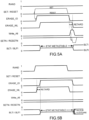
- the timelines of Figures 5A, 5B are respectively representative of a sequence of signals implemented by the initialization circuit 100 for the realization of a deterministic initialization and of another sequence of signals this time implemented by this same initialization circuit 100 for the implementation of a free initialization.
- the initialization circuit 100 located at the periphery of the matrix plane M 1 is here equipped with an asynchronous logic control block 140 receiving as input asynchronous logic signals RESET, RAND, SET, respectively of deterministic initialization to zero, of triggering of free initialization, and deterministic initialization trigger to one.
- a change of state of the deterministic initialization trigger signal SET can be caused for example following detection of a fraudulent attempt to access the memory, this detection being able itself to result in the transmission or change status of a fraudulent access detection signal S AF .
- the signal SET goes in particular to a logic state '1', which first of all triggers an erasing phase.
- the change of state of the signal SET causes a change of state of a signal ERASE called “erasure” on which a sequence of control signals ERASE_IO, ERASE_WL depends.
- the erase signal ERASE is produced at the output of a stage 141 of the control block 140 receiving as input the signal SET for triggering deterministic initialization, the signal RAND for triggering free initialization, the signal RESET, and performing a OR function between these signals.
- Stage 141 is in the particular embodiment illustrated, formed by a logic gate, in particular performing an OR function.
- the high supply line VirVDD of the memory cells to be initialized can be disconnected (left floating) or grounded. It is in any case decoupled from an element of the grid type or supply line brought to the supply potential VDD. At least one of the inverters and advantageously the two inverters are then not powered.
- the initialization circuit is advantageously provided with a switch element controlled by a first control signal ERASE_IO and configured to, following a change of state of this first control signal ERASE_IO, make it possible to disconnect said line from VirVDD high supply of the supply network carrying a VDD supply potential.
- the switch element is in the form of a transistor 161, here of the PMOS type, receiving on its gate the first control signal ERASE_IO and placed between the supply network set to a potential VDD and the line VirVDD high power supply.
- An erasing phase of a deterministic initialization is here triggered by a signal SET or RESET rising to a logic level '1'.
- the signals SET_latch, RESET-latch can be input flip-flop output signals respectively receiving the signals SET and RESET, the logic signal RESET-latch being complementary to the logic signal SET_latch.
- the first control signal ERASE_IO follows the same evolution as the erasing signal ERASE.
- the first control signal ERASE_IO can in particular be produced at the output of a first multiplexer 144 with two '0' and '1' inputs and whose selection signal is the free initialization trigger signal RAND, in this mode of operation deactivated and therefore maintained at a logic '0' state.
- the first multiplexer 144 receives on its first input (input '0') the erase signal ERASE and on its second input (input '1') an output signal from a delay stage 142, this output signal corresponding to the erasing signal ERASE with a predetermined delay.
- the internal nodes NF, NT of the memory cells which it is desired to initialize are equalized: they are set to equal or substantially equal potentials (ie to values which differ by less than 10 mV).
- Such an erasing phase makes it possible to implement several initialization modes while limiting the number of components necessary for this implementation and limiting the time necessary to perform each initialization.
- the equalization of the nodes NF, NT of the cells of the i-th column is carried out by connecting together the lines of bit BLTi and BLFi and by coupling these bit lines BLTi and BLFi to these nodes NF, NT through the access transistors TA T and TA F .
- another switch element formed for example of an N-type transistor 171 whose gate electrode is controlled by the first control signal ERASE_IO can be provided between the bit lines BLTi and BLFi.
- the first control signal ERASE_IO it is possible alternatively to connect the bit lines BLTi and BLFi together when it is desired to perform an erasure, or else to disconnect the bit lines BLTi from each other and BLFi to allow the establishment of the nodes NF, NT at respective values different from each other.
- bit lines BLTi and BLFi When the bit lines BLTi and BLFi are connected together (first control signal ERASE_IO at level '1' on the figure 5A ), these bit lines BLTi and BLFi can also be isolated from bias lines 193, 194 placed, for example, at potential VDD of an IO circuit peripheral to the memory plane and located at one end of the column of cells, generally at the bottom of column.
- a switch element is thus provided to alternately provide coupling or decoupling between the first bit line BLTi and the first bias line 193.
- a switch element is provided to alternately provide coupling or decoupling. decoupling between the second bit line BLF and the second bias line 194.
- these switching elements are in the form of coupling transistors 191, 192, for example of the PMOS type.
- the gates of transistors 191, 192 are here controlled respectively by a first control signal SETN and another control signal RESETN.
- control signals SETN and RESETN are output signals respectively from a first logic block 157 performing a NAND logic function (NAND) and from a second logic block 159 performing a NAND function.
- the first logic block 157 here has an input controlled by the logic signal SET_latch while the second logic block 159 has an input controlled by the logic signal RESET-latch complementary to the first logic signal SET_latch.
- the two logic blocks 157, 159 also have a common input controlled by a simultaneous write trigger signal Write_all, itself dependent on a second control signal ERASE_WL, the first control signal ERASE_IO and the free initialization trigger signal RAND.
- the simultaneous write triggering signal Write_all is produced at the output of a block 151 performing a NOT OR (NOR) function and receiving as input a signal not(ERASE_WL) complementary to the second signal of control signal ERASE_WL, the first control signal ERASE_IO and the trigger signal RAND.
- means or a selection stage integrated into a row decoder R_DEC of the memory plane comprise an additional line 182 provided for conveying the second control signal ERASE_WL serving word line simultaneous selection signal.
- a transistor 181 is provided, the gate of which is connected to the additional row 182 carrying the control signal ERASE_WL.
- Transistor 181 whose gate is controlled by signal ERASE_WL, is connected to the input of an inverter circuit WD located at the output of row decoder R_DEC.
- the transistor 181 is of the N type and the simultaneous selection is performed here when the second control signal ERASE_WL routed on the additional line 182 is set to a logic '1' level.
- the second control signal ERASE_WL can in particular be produced at the output of a second multiplexer 143 with two '0' and '1' inputs and whose selection signal is the free initialization trigger signal RAND.
- the second multiplexer 143 receives on its first input (input '0') the output signal of the delay stage 142, this output signal corresponding to the erasing signal ERASE with a predetermined delay.
- the multiplexers 144, 143 are thus controlled by the same selection signal and have inverted inputs with respect to each other, so that the first input of the first multiplexer is connected to the second input of the second multiplexer while the second input of the first multiplexer is connected to the first input of the second multiplexer.
- a new state change of the SET signal (in the example of the figure 5A switching again to the logic state '0') of deterministic initialization trigger ends the erasing phase and causes a change of state of the first control signal ERASE_IO, so as to decouple between them the first node NT and the second NF node here by disconnecting the first bit line BLTi from the second bit line BLFi.
- the change of state of the first control signal ERASE_IO also makes it possible to restore the power supply to the cells by reconnecting, via the transistor 161 turned on, the high power supply line virVDD to the power supply gate grounded. VDD supply potential.
- the transition to state '0' of the first control signal ERASE_IO also triggers a transition to state '1' of the simultaneous write signal Write_All.
- This transition to state '1' of the simultaneous write signal Write_All causes a change of state of the control signal SETN, here activated or set to a logic state '0', so as to couple the first bit line BLTi to bias line 193 to supply potential VDD.
- the second bit line BLFi remains decoupled from the bias line 194 insofar as the other control signal RESETN is maintained in the same logic state '1'.
- the second control signal ERASE_WL is maintained at state '1', which makes it possible to maintain the access transistors activated, by creating a bias imbalance between the first bit line and the second bit line, thus forces the simultaneous writing of a datum, here a value '1' in the NT nodes of all the cells whose word line has been activated.
- the duration of the simultaneous writing depends and can be in particular equal to the predetermined delay imposed by the stage 142.
- the phase is concluded, is the operation just carried out ( SET or RESET) remains stored in the SET_LATCH and RESET_LATCH signals.
- the probability that a memory cell initializes to 1 is equal to 1 if we do a SET: p(P, V SR , VDD, T) of the Figure 7B therefore has a single peak on value '1'.
- the probability that a cell is initialized at 0 is equal to 1 if we do a RESET: p(P, V SR , -VDD, T) therefore has a single peak at the value '0'.
- the clearing phase of a free initialization is triggered by a RAND signal rising to a logic level '1', example illustrated on the figure 5B .
- the change of state of the trigger signal RAND first triggers a blanking phase here as well.
- the first control signal ERASE_IO is this time delayed with respect to the second control signal ERASE_WL by the predetermined delay imposed by the delay stage 142.
- a change of state of the first control signal ERASE_IO following that of the second control signal signal ERASE_WL causes a disconnection of the high supply line virVDD of the cells and an equalization ("METASTABLE STATE" of signals BLTi, BLFi respectively of bit lines of an i-th column on the figure 5B ) of the potential values of the first node NT and the second node NF, again through a connection between them of the bit lines BLTi and BLFi while the access transistors are activated.
- the control signals SETN and RESETN are moreover here kept deactivated (ie at '1') so as to decouple the bit lines BLTi and BLFi from the additional bias lines 192, 193 throughout the duration of the operating mode. free initialization.
- the high supply line virVDD is decoupled from an element 199 such as a supply gate or a supply line at the supply potential VDD. This decoupling is achieved here by means of a transistor 161 made off.
- the first inverter INV1 and the second inverter INV2 are then not powered.
- a new change of state of the trigger RAND signal causes a change of state of the second control signal ERASE _WL, which causes the end of the simultaneous selection of the word lines, then, a change of state of the first signal of order ERASE_IO.
- This change of state here the setting to '0' of the first command signal ERASE_IO leads to the end of the pre-initialization phase and the equalization of the nodes. This triggers a disconnection of the bitlines BLTi and BLFi from each other.
- This change of state of the first control signal ERASE_IO also causes a reconnection of the high supply line VirVDD of the cells to a supply grid. The high supply line VirVDD is then restored to a supply potential VDD.
- the first inverter INV1 and the second inverter INV2 are then powered.
- Each cell can then individually switch to a value '1' or '0' (corresponding for example by convention to a logical state '1' or '0' of their first NT node) in a free or random way, but which follows the statistic ⁇ (V SR , 0, T) depends on the local variations and the operating conditions specific to this cell and to the chip to which it belongs. Thus, some cells are then set to a logic '1' state while others are set to a logic '0' state.
- the initialization circuit makes it possible to use one or the other of these two techniques alternatively while limiting the number of components necessary and the consumption generated by the initialization.
- the initialization circuit also makes it possible to accelerate the deterministic writing of all or a subset of the memory to a value set by the user or the designer of the memory, thanks to the presence and the control method of the transistors connected to the supply networks 191 and 192.
- the erasing phase during which the first node NT and the second node NF of each cell are equalized can be carried out by forcing the bit lines to ground .
- 6T memory cells which include, as shown in figure 1B , an erase transistor T 1 although this is less advantageous in terms of compactness and integration density.
- erasing no longer requires having transistor 171 at the bottom of the column.
- the control logic can then be adapted to control the conduction of the erasing transistors in each cell thanks to a control signal for these erasing transistors which can be similar to that of the signal ERASE_IO.
- the activation of the ERASE_WL signal is then no longer necessary in this erasing phase and it is possibly possible to overcome the presence of this ERASE_IO signal with the associated transistors 181.
- NMOS transistors connected to ground lines instead of PMOS transistors connected to supply lines 193 and 194 set to VDD.
- an "analog" adjustment of the current or the voltage to be imposed on one or the other of the bit lines during the second initialization phase is carried out, in particular by applying a current or a voltage on the intermediate bit line with respect to that (the one) applied when the bit line is coupled to ground or to the supply potential VDD, and this, in order to obtain a random draw associated with a probability different from a "standard” probability defined when applying a supply potential VDD or ground GND.
- a simultaneous selection of the cells is carried out by activating at least several word lines and consequently the access transistors of at least several rows of cells.
- provision can be made to keep the word lines of the rows of cells that it is desired to initialize deactivated.
- the access transistors of the cells belonging to these rows are then kept deactivated to block access to the cell and to decouple the latter from the bit lines.
- Such a “partially deterministic” mode of initialization can be used in order, for example, to accelerate a research phase ("enrollment” according to Anglo-Saxon technology) of highly biased memory cells, i.e. to say which, when they are initialized, initialize preferentially according to a value '1' or '0' under conditions of temperature and voltage varying in a given range.
- Such a “biased” mode of initialization makes it possible to carry out an initialization which will have an intermediate statistic between these extreme cases, and therefore to alter the free initialization by favoring the state '0' if ⁇ V ⁇ 0 or rather the state '1' if ⁇ V>0.
- the voltage values applied to the bit lines BLTi, BLFi therefore allow us to control the initialization statistics.
- This "partially biased" initialization mode can be implemented by introducing a conductivity imbalance between the transistors arranged between the bit line of a bias line.
- This imbalance adjustable according to the bias that one wishes introduced, can be adjusted by adapting the respective sizing of the transistors, and in particular their W/L ratio (ratio of the width to the length of the channel) either by adapting their respective biases, or by a combination of these two types of adaptations .
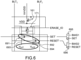
- a coupling transistor 691 is provided, this transistor 691 this time being of the NMOS type and provided with a gate controlled by the signal SET'.
- This signal SET' can take the value of the signal SET, when it is desired to carry out a deterministic or free initialization.
- This signal SET' can on the other hand take the value of a bias signal BIAS1, when it is desired to perform a biased initialization.
- a coupling transistor 692 here also of the NMOS type, and provided with a gate controlled by the signal RESET', is provided between the second bit line BLF and a second bias line 694 brought to a second potential of Vpol2 polarization.
- This signal RESET' can take the value of the signal RESET, when it is desired to carry out a deterministic or free initialization.
- This signal can take the value of another bias signal BIAS2, when it is desired to perform a biased initialization.
- the first transistor 691 can be provided with a ratio W1/L1 different from that W2/L2 of the second transistor 692. Whereas in the example described above in connection with the figure 4 , transistors of large size are typically chosen, transistors 691, 692 of small size can be provided here.
- Vpol1, Vpol2 are advantageously provided equal to ⁇ V, with ⁇ V ⁇ VDD, VDD being the supply potential VDD.
- ⁇ V ⁇ VDD ⁇ V much lower than VDD
- ⁇ V is at least lower than VDD/10 and advantageously lower than VDD/Y
- a different bias is ensured between the first bit line BLTi and the second bit line BLFi while activating the first access transistor and the second access transistor of the initialized cells .
- the voltage or current level imposed on the bit line coupled to the transistor made conductive is different from that making it possible to impose a given state with a probability level close to '1' so that the level at which the initialized cells remain random.
- the bias difference between the bit lines is this time performed by keeping the bias difference between the two bit lines at a low ⁇ V level and much lower than the supply potential VDD in order to bias the trend of the NT and NF nodes to switch to a logical value or a given state without, however, imposing it.
- the value of ⁇ V can be modulated according to the bias that it is desired to introduce. In modifying this value, the probability that a cell settles at a level '1' or '0' is modified.
- the complete sequence of values ⁇ V i can be determined by an algorithm, so as to select the most strongly biased cells. A detection of highly biased cells can thus be implemented.
- the memory According to a variant of use of the memory, it is possible to search for the memory cells presenting a probability of 0.5 or another value which may be different from the extreme values close to 0 or 1. To do this, tests are carried out on the cells memories with a free initialization with zero or given asymmetry in the polarizations. It is then possible to list for each cell what is its probability p ijk of taking a given value, for example '1', for each level of asymmetry as a function of the polarization bias.
- the probability p ijk that a given cell initializes to a value '1' is centered on 0.5, it can be advantageously used to generate, during a free initialization, a random binary number with maximum entropy, having therefore an equal probability 0.5 of bringing out the value 1 or 0.
- a free initialization can be implemented with the introduction of a polarization bias making it possible to have the desired probability.
- An implementation as described previously in connection with the figure 6 is particularly favorable to the implementation within the same circuit, of a memory, a random number generator and an in-memory calculation module (IMC for “In Memory Computing”) in particular allowing to perform a certain function such as a MAC function (for “multiply-and-accumulate”, ie “multiply then accumulate”).
- IMC in-memory calculation module
- a device as implemented according to one or other of the embodiments described above can find applications in particular in embedded systems, in HPC high performance computing systems for (“High Performance Computing”) and/or encryption such as AES systems (for “Advanced Encryption Standard”, i.e. “advanced encryption standard”) of cryptocurrency systems.
- HPC high performance computing systems for (“High Performance Computing”) and/or encryption such as AES systems (for “Advanced Encryption Standard”, i.e. “advanced encryption standard”) of cryptocurrency systems.
Landscapes
- Engineering & Computer Science (AREA)
- Microelectronics & Electronic Packaging (AREA)
- Computer Hardware Design (AREA)
- Power Engineering (AREA)
- Static Random-Access Memory (AREA)
- Logic Circuits (AREA)
Applications Claiming Priority (1)
| Application Number | Priority Date | Filing Date | Title |
|---|---|---|---|
| FR2111286A FR3128570B1 (fr) | 2021-10-25 | 2021-10-25 | Sram a initialisation reconfigurable |
Publications (1)
| Publication Number | Publication Date |
|---|---|
| EP4170655A1 true EP4170655A1 (de) | 2023-04-26 |
Family
ID=79170705
Family Applications (1)
| Application Number | Title | Priority Date | Filing Date |
|---|---|---|---|
| EP22198595.5A Pending EP4170655A1 (de) | 2021-10-25 | 2022-09-29 | Sram mit rekonfigurierbarer initialisierung |
Country Status (3)
| Country | Link |
|---|---|
| US (1) | US12362011B2 (de) |
| EP (1) | EP4170655A1 (de) |
| FR (1) | FR3128570B1 (de) |
Cited By (1)
| Publication number | Priority date | Publication date | Assignee | Title |
|---|---|---|---|---|
| FR3153183A1 (fr) * | 2023-09-19 | 2025-03-21 | Commissariat A L'energie Atomique Et Aux Energies Alternatives | Dispositif ameliore de gestion d’initialisation de memoire sram |
Families Citing this family (3)
| Publication number | Priority date | Publication date | Assignee | Title |
|---|---|---|---|---|
| FR3144403B1 (fr) | 2022-12-21 | 2025-07-25 | Commissariat Energie Atomique | Sram avec mise en veille de secteur dedie au puf |
| CN116312671B (zh) * | 2023-05-19 | 2023-08-29 | 珠海妙存科技有限公司 | 一种sram重置方法、电路、芯片、装置与介质 |
| FR3154224A1 (fr) | 2023-10-12 | 2025-04-18 | Commissariat A L'energie Atomique Et Aux Energies Alternatives | Generation cle cryptographique a partir d’une memoire sram |
Citations (3)
| Publication number | Priority date | Publication date | Assignee | Title |
|---|---|---|---|---|
| US20180096172A1 (en) * | 2016-10-04 | 2018-04-05 | Taiwan Semiconductor Manufacturing Co., Ltd. | Self-destruct sram-based authentication circuit |
| EP3496101A1 (de) * | 2017-12-06 | 2019-06-12 | Commissariat à l'énergie atomique et aux énergies alternatives | Sram-speicher mit schneller löschfunktion |
| US20190392179A1 (en) * | 2018-06-26 | 2019-12-26 | Taiwan Semiconductor Manufacturing Co., Ltd. | Method and apparatus for protecting a puf generator |
Family Cites Families (4)
| Publication number | Priority date | Publication date | Assignee | Title |
|---|---|---|---|---|
| FR2760286B1 (fr) * | 1997-02-28 | 1999-04-16 | Sgs Thomson Microelectronics | Procede d'effacement d'une memoire ram statique et memoire en circuit integre associe |
| US20080019162A1 (en) * | 2006-07-21 | 2008-01-24 | Taku Ogura | Non-volatile semiconductor storage device |
| FR3106692B1 (fr) * | 2020-01-27 | 2024-01-19 | St Microelectronics Rousset | Dispositif de mémoire vive statique non-volatile et procédé de commande correspondant. |
| JP7430425B2 (ja) * | 2020-02-10 | 2024-02-13 | 国立研究開発法人科学技術振興機構 | 双安定回路および電子回路 |
-
2021
- 2021-10-25 FR FR2111286A patent/FR3128570B1/fr active Active
-
2022
- 2022-09-29 EP EP22198595.5A patent/EP4170655A1/de active Pending
- 2022-10-12 US US18/045,881 patent/US12362011B2/en active Active
Patent Citations (3)
| Publication number | Priority date | Publication date | Assignee | Title |
|---|---|---|---|---|
| US20180096172A1 (en) * | 2016-10-04 | 2018-04-05 | Taiwan Semiconductor Manufacturing Co., Ltd. | Self-destruct sram-based authentication circuit |
| EP3496101A1 (de) * | 2017-12-06 | 2019-06-12 | Commissariat à l'énergie atomique et aux énergies alternatives | Sram-speicher mit schneller löschfunktion |
| US20190392179A1 (en) * | 2018-06-26 | 2019-12-26 | Taiwan Semiconductor Manufacturing Co., Ltd. | Method and apparatus for protecting a puf generator |
Cited By (2)
| Publication number | Priority date | Publication date | Assignee | Title |
|---|---|---|---|---|
| FR3153183A1 (fr) * | 2023-09-19 | 2025-03-21 | Commissariat A L'energie Atomique Et Aux Energies Alternatives | Dispositif ameliore de gestion d’initialisation de memoire sram |
| EP4528735A1 (de) * | 2023-09-19 | 2025-03-26 | Commissariat à l'Energie Atomique et aux Energies Alternatives | Verbesserte sram-speicherinitialisierungsverwaltungsvorrichtung |
Also Published As
| Publication number | Publication date |
|---|---|
| US20230127142A1 (en) | 2023-04-27 |
| FR3128570A1 (fr) | 2023-04-28 |
| FR3128570B1 (fr) | 2023-10-27 |
| US12362011B2 (en) | 2025-07-15 |
Similar Documents
| Publication | Publication Date | Title |
|---|---|---|
| EP4170655A1 (de) | Sram mit rekonfigurierbarer initialisierung | |
| EP2842229B1 (de) | Reprogrammierbare logische vorrichtung mit strahlenwiderstandsfähigkeit | |
| EP3092646B1 (de) | Verfahren und schaltung zur programmierung nichtflüchtiger speicherzellen eines flüchtigen/nichtflüchtigen speicherarray | |
| FR2825829A1 (fr) | Dispositif de memoire a semiconducteur ayant des reseaux de cellules de memoire permettant un acces selectif | |
| FR2957449A1 (fr) | Micro-amplificateur de lecture pour memoire | |
| FR2974666A1 (fr) | Amplificateur de detection differentiel sans transistor de precharge dedie | |
| FR2974667A1 (fr) | Amplificateur de detection differentiel sans transistor de commutation | |
| EP3002788B1 (de) | Vorrichtung mit sram-speicherzellen die mitteln zur polarisierung der wannen der speicherzelltransistoren umfasst | |
| EP3496101A1 (de) | Sram-speicher mit schneller löschfunktion | |
| FR2927722A1 (fr) | Cellule memoire sram a transistor double grille dotee de moyens pour ameliorer la marge en ecriture | |
| FR2948811A1 (fr) | Dispositif de memoire statique a cinq transistors et procede de fonctionnement | |
| EP3633677A1 (de) | Imc-speicherschaltkreis mit 6t-zellen | |
| EP3373303A1 (de) | Tfet-speicherlatch ohne aktualisierung | |
| FR2805369A1 (fr) | Structure de registre avec un mecanisme d'ecriture symetrique | |
| EP3598451B1 (de) | Sram-/rom-speicher, der durch verbindungen zu den versorgungsanschlüssen rekonfigurierbar ist | |
| EP4020479B1 (de) | Differentielles lesen eines rram-speichers mit geringem stromverbrauch | |
| EP4390930A1 (de) | Sram mit puf-different-sektor-aufrechterhaltung | |
| FR3044460A1 (fr) | Amplificateur de lecture pour memoire, en particulier une memoire eeprom | |
| FR2552257A1 (fr) | Circuit decodeur pour memoire ram statique | |
| EP4539390A1 (de) | Kryptographische schlüsselerzeugung aus einem sram-speicher | |
| EP4390929A1 (de) | Sram-speicher mit deterministischer zufallsinitialisierung | |
| EP4528735A1 (de) | Verbesserte sram-speicherinitialisierungsverwaltungsvorrichtung | |
| EP4345820B1 (de) | Schaltung zum zerstörungsfreien auslesen ferroelektrischer speicher | |
| EP3680904A1 (de) | Detektionsschaltkreis eines vorherrschenden dateninhalts in einer speicherzelle | |
| FR3055735A1 (fr) | Amplificateur de detection apte a controler une operation de lecture dans une memoire |
Legal Events
| Date | Code | Title | Description |
|---|---|---|---|
| PUAI | Public reference made under article 153(3) epc to a published international application that has entered the european phase |
Free format text: ORIGINAL CODE: 0009012 |
|
| STAA | Information on the status of an ep patent application or granted ep patent |
Free format text: STATUS: REQUEST FOR EXAMINATION WAS MADE |
|
| 17P | Request for examination filed |
Effective date: 20220929 |
|
| AK | Designated contracting states |
Kind code of ref document: A1 Designated state(s): AL AT BE BG CH CY CZ DE DK EE ES FI FR GB GR HR HU IE IS IT LI LT LU LV MC MK MT NL NO PL PT RO RS SE SI SK SM TR |
|
| RAP3 | Party data changed (applicant data changed or rights of an application transferred) |
Owner name: COMMISSARIAT A L'ENERGIE ATOMIQUE ET AUX ENERGIESALTERNATIVES |
|
| STAA | Information on the status of an ep patent application or granted ep patent |
Free format text: STATUS: EXAMINATION IS IN PROGRESS |
|
| 17Q | First examination report despatched |
Effective date: 20250326 |