EP4164134B1 - Kommunikationsvorrichtung und betriebsverfahren - Google Patents
Kommunikationsvorrichtung und betriebsverfahren Download PDFInfo
- Publication number
- EP4164134B1 EP4164134B1 EP21201236.3A EP21201236A EP4164134B1 EP 4164134 B1 EP4164134 B1 EP 4164134B1 EP 21201236 A EP21201236 A EP 21201236A EP 4164134 B1 EP4164134 B1 EP 4164134B1
- Authority
- EP
- European Patent Office
- Prior art keywords
- receiver
- receiver circuit
- mode
- controller
- signal
- Prior art date
- Legal status (The legal status is an assumption and is not a legal conclusion. Google has not performed a legal analysis and makes no representation as to the accuracy of the status listed.)
- Active
Links
Images


Classifications
-
- H—ELECTRICITY
- H04—ELECTRIC COMMUNICATION TECHNIQUE
- H04B—TRANSMISSION
- H04B1/00—Details of transmission systems, not covered by a single one of groups H04B3/00 - H04B13/00; Details of transmission systems not characterised by the medium used for transmission
- H04B1/69—Spread spectrum techniques
- H04B1/7163—Spread spectrum techniques using impulse radio
- H04B1/7183—Synchronisation
-
- H—ELECTRICITY
- H04—ELECTRIC COMMUNICATION TECHNIQUE
- H04B—TRANSMISSION
- H04B1/00—Details of transmission systems, not covered by a single one of groups H04B3/00 - H04B13/00; Details of transmission systems not characterised by the medium used for transmission
- H04B1/06—Receivers
- H04B1/16—Circuits
- H04B1/1638—Special circuits to enhance selectivity of receivers not otherwise provided for
-
- H—ELECTRICITY
- H04—ELECTRIC COMMUNICATION TECHNIQUE
- H04B—TRANSMISSION
- H04B1/00—Details of transmission systems, not covered by a single one of groups H04B3/00 - H04B13/00; Details of transmission systems not characterised by the medium used for transmission
- H04B1/69—Spread spectrum techniques
- H04B1/7163—Spread spectrum techniques using impulse radio
- H04B1/71637—Receiver aspects
-
- H—ELECTRICITY
- H04—ELECTRIC COMMUNICATION TECHNIQUE
- H04B—TRANSMISSION
- H04B2201/00—Indexing scheme relating to details of transmission systems not covered by a single group of H04B3/00 - H04B13/00
- H04B2201/69—Orthogonal indexing scheme relating to spread spectrum techniques in general
- H04B2201/7163—Orthogonal indexing scheme relating to impulse radio
- H04B2201/71634—Applied to ranging
Definitions
- the present disclosure relates to a communication device. Furthermore, the present disclosure relates to a corresponding method of operating a communication device.
- Ultra-wideband (UWB) communication technology is a technology that uses a high signal bandwidth, in particular for transmitting digital data over a wide spectrum of frequency bands with very low power.
- UWB technology may use the frequency spectrum of 3.1 to 10.6 GHz and may feature a high-frequency bandwidth of more than 500 MHz and very short pulse signals, potentially capable of supporting high data rates.
- the UWB technology enables a high data throughput for communication devices and a high precision for the localization of devices.
- UWB technology may be used for so-called ranging operations, i.e. for determining the distance between communicating devices. Therefore, UWB technology may be used to advantage in various applications, such as automotive applications.
- EP 3 745 606 A1 describes a method for operating an ultra-wideband (UWB) device.
- the method involves powering down a first receive path of a multipath UWB device while leaving a second receive path of the multipath UWB device powered up, powering down channel estimation, tracking, and demodulation functions of the second receive path, and performing an acquisition function using the second receive path while the first receive path is powered down and while the channel estimation, tracking, and demodulation functions of the second receive path are powered down.
- UWB ultra-wideband
- the controller is further configured to switch the receiver circuit from the real receiver mode to the complex receiver mode upon or after a successful acquisition of the signal.
- the successful acquisition of the signal is based on the detection of a synchronization field within said signal, wherein the synchronization field is included in a data frame.
- the controller is further configured to wake up the receiver circuit before switching the receiver circuit from the real receiver mode to the complex receiver mode.
- the controller is further configured to wake up the receiver circuit after switching the receiver circuit from the real receiver mode to the complex receiver mode.
- the controller is further configured to reset a center frequency upon or after switching the receiver circuit from the real receiver mode to the complex receiver mode.
- the receiver circuit is configured to operate in the complex receiver mode by default, and the controller is configured to switch the receiver circuit from the complex receiver mode to the real receiver mode if no signal is found within a predefined amount of time after the receiver circuit has started up.
- the device is an ultra-wideband (UWB) communication node acting as a responder in a communication system.
- UWB ultra-wideband
- a method of operating a communication device is conceived, as defined in claim 9.
- UWB communication technology is a technology that uses a high signal bandwidth, in particular for transmitting digital data over a wide spectrum of frequency bands with very low power.
- UWB technology may use the frequency spectrum of 3.1 to 10.6 GHz and may feature a high-frequency bandwidth of more than 500 MHz and very short pulse signals, potentially capable of supporting high data rates.
- the UWB technology enables a high data throughput for communication devices and a high precision for the localization of devices.
- UWB technology may be used for so-called ranging operations, i.e. for determining the distance between communicating devices. Therefore, UWB technology may be used to advantage in various applications, such as automotive applications.
- UWB communication devices may have a relatively high power or current consumption. This is especially true for a responding transceiver ("responder"), when the timing relationship to an initiating transceiver (“initiator”) is not established. The responder will be in a constant receive mode for a potentially long time period, waiting for the first frame.
- high performance UWB receivers tend to have high current consumption in the receive mode. This is mainly caused by an analog-to-digital converter (ADC) sampling rate and digital processing rate in the 1GHz frequency range, by a 500MHz bandwidth of the analog frontend, and by a local oscillator (LO) distribution in the 10GHz frequency range.
- ADC analog-to-digital converter
- LO local oscillator
- Two quadrature receive (Rx) paths are used to guarantee optimal reception, even if the LO phases of the sender and receiver are not phase aligned.
- the bill of materials (BOM) and size of a UWB communication device are typically determined by the current consumption in a constant Rx mode.
- a transceiver typically contains a signal transmission function or signal transmission unit (i.e., a transmitter) and a signal receiving function or signal receiving unit (i.e., a receiver).
- the receiver is capable of receiving a radio frequency (RF) signal.
- Receivers are often based on an IQ topology. It is noted that, according to the IQ topology, a received signal is divided into an I-component or I-channel and a Q-component or Q-channel.
- the I-channel is the received RF signal without a phase shift (i.e., the "in-phase" or reference signal), while the Q-channel is the received signal shifted by 90 degrees (i.e., the received signal in quadrature).
- the RF signal is typically mixed with two sinusoids (i.e. LO outputs), where one sinusoid has a pi/2 phase offset relative to the other sinusoid. If only the I-channel is enabled, the receiver effectively operates in a real receiver mode, while if both the I-channel and the Q-channel are enabled, the receiver effectively operates in a complex receiver mode. Alternatively, the receiver may effectively operate in the real receiver mode if only the Q-channel is enabled.
- two sinusoids i.e. LO outputs
- Fig. 1 shows an illustrative embodiment of a communication device 100.
- the communication device 100 comprises a receiver circuit 102 and a controller 104 which are operatively coupled to each other.
- the receiver circuit 102 is configured to receive a signal from an external communication device (not shown).
- the controller 104 is configured to control said receiver circuit 102, wherein said controller 104 is configured to cause said receiver circuit 102 to operate either in a complex receiver mode or in a real receiver mode. More specifically, the controller 104 is configured to cause said receiver circuit 102 to operate in the real receiver mode until the signal is successfully acquired. In particular, it may be sufficient to operate the receiver circuit 102 in the real receiver mode if the signal has not yet been acquired successfully. Since the real receiver mode requires less power than the complex receiver mode, the power consumption of the communication device 100 may be reduced significantly.
- the controller is further configured to cause the receiver circuit to use, in the complex receiver mode, an I-channel and a Q-channel of the received signal. In this way, a practical implementation of the complex receiver mode may be realized. Furthermore, the controller is further configured to cause the receiver circuit to use, in the real receiver mode, only said I-channel of the received signal or only said Q-channel of the received signal. In this way, a practical implementation of the real receiver mode may be realized.
- the controller is further configured to apply, when the receiver circuit operates in the real receiver mode, a local oscillator frequency which is different from the local oscillator frequency applied when the receiver operates in the complex receiver mode. Furthermore, the controller is configured to offset, when the receiver circuit operates in the real receiver mode, the local oscillator frequency of the receiver circuit by a fraction of the chip rate. In this way, the reception of the signal is facilitated, such that the signal can be properly acquired.
- a chip is equivalent to a UWB pulse. Accordingly, the transmission rate of the pulses may be referred to as the chip rate.
- the maximal transmission rate is defined in the IEEE 14.5 HRP standard as 499.2 MHz.
- the controller is further configured to switch the receiver circuit from the real receiver mode to the complex receiver mode upon or after a successful acquisition of the signal.
- the receiver circuit may perform at full performance when the signal has been acquired and the contents of the signal should be processed.
- the successful acquisition of the signal is based on the detection of a synchronization field within said signal, wherein the synchronization field is included in a data frame. In this way, it can easily be determined whether the signal has been successfully acquired.
- the controller is further configured to wake up the receiver circuit before switching the receiver circuit from the real receiver mode to the complex receiver mode. This may be advantageous in some implementations of the communication device. Alternatively, the controller is further configured to wake up the receiver circuit after switching the receiver circuit from the real receiver mode to the complex receiver mode. This may be advantageous in other implementations of the communication device. Furthermore, in one or more embodiments, the controller is configured to reset a center frequency upon or after switching the receiver circuit from the real receiver mode to the complex receiver mode. This has the advantage that a data part of a first frame may be received with full sensitivity.
- the receiver circuit is configured to operate in the complex receiver mode by default, and the controller is configured to switch the receiver circuit from the complex receiver mode to the real receiver mode if no signal is found within a predefined amount of time after the receiver circuit has started up. This may be advantageous in systems in which a wake-up event is triggered via a separate interface.
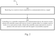
- Fig. 2 shows an illustrative embodiment of a method 200 of operating a communication device.
- the method 200 comprises the following steps.
- a receiver circuit comprised in a communication device receives a signal. More specifically, the receiver circuit receives a signal from an external communication device.
- a controller comprised in the communication device controls the receiver circuit, wherein the controller causes said receiver circuit to operate either in a complex receiver mode or in a real receiver mode. More specifically, the controller causes said receiver circuit to operate in the real receiver mode until the signal is successfully acquired. As explained above, it may be sufficient to operate the receiver circuit in the real receiver mode if the signal has not yet been acquired successfully. Since the real receiver mode requires less power than the complex receiver mode, the power consumption of the communication device may be reduced significantly.
- the local oscillator (LO) frequency of the RX may be offset by a carrier frequency offset (CFO) that is a fraction of the chip rate (e.g. 1/8, 1/4, 1/2 of 499.2 MHz).
- CFO carrier frequency offset
- the digital receiver may be capable of receiving the frame with said CFO.
- This method may be compatible with different ranging protocols, such as the protocols defined by the Institute of Electrical and Electronics Engineers (IEEE), the Car Connectivity Consortium (CCC) and the FiRa Consortium.
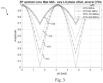
- Fig. 3 shows a maximum amplitude 300 of an I-component relative to an LO phase offset for several carrier frequency offsets (CFOs).
- the LO phase offset is a frequency offset between the receiver (RX) and the transmitter (TX).
- UWB receivers typically use an in-phase component (i.e., an I-component) and a quadrature component (i.e., a Q-component).
- the RF signal is typically mixed with two sinusoids (i.e. LO outputs), where one sinusoid has a pi/2 phase offset relative to the other sinusoid.
- Line 302 shows a regular case with no frequency offset. Then, the amplitude highly depends on the phase offset between the LOs.
- the controller may be configured to offset, when the receiver circuit operates in the real receiver mode (i.e., when only the I-component is enabled), the local oscillator frequency of the receiver circuit by a fraction of the chip rate.
- Line 306 shows an example of such an offset. More specifically, line 306 shows a frequency offset by 1 ⁇ 4 of the chip rate.
- the amplitude still depends on the LO phase offset and the minimum is approximately 42% of the maximum (i.e., the performance loss is approximately 7.5dB).
- the performance loss is approximately 7.5dB.
- the UWB signal amplitudes can be below the noise floor at the receiver circuit.
- the receiver circuit typically employs correlation to recover the signal.
- the correlation is sensitive to frequency offsets and small offsets in the range of 10s of ppm can destroy the signal.
- Fig. 5 shows an illustrative embodiment of a field structure of a full frame 500.
- this field structure is specified in the technical standard " IEEE Standard for Low-Rate Wireless Networks", IEEE Std 802.15.4-2020 (Revision of IEEE Std 802.15.4-2015), 23 July 2020, doi: 10.1109/IEEESTD.2020.9144691 .
- For a wake up receiver it may be important that it can also receive the data part (containing a physical layer packet header (PHR) and a PHY payload) of a frame, in order to comply with existing protocols, such as the protocols defined by the IEEE, CCC and FiRa Consortium, and in order to start the ranging protocol with the first frame.
- PHR physical layer packet header
- the data part is typically modulated with a higher maximal chip rate than the synchronization header (SHR).
- the IEEE 15.4z standard defines two options, i.e. a burst with back-to-back chips and a burst with guard chips.
- a chip is equivalent to a UWB pulse.
- the time period Tc indicates the duration of one chip. Accordingly, the digital receiver may have to be designed to receive the PHR and payload of a frame with a CFO that is a fraction of the maximal chip rate.
- the reception of the SYNC field of the first frame may wake up 606 the device, and the data part of the frame may be ignored.
- the receiver circuit may be started 608 and both the I-component and the Q-component may be enabled. Accordingly, the following frames are received with full receiver performance. This procedure is most suited for systems in which a transmitter sends wake-up frames at regular intervals, and in which it is not critical that the receiver receives the payload of the first frame. For example, for a wearable smart tag the response time is not critical.
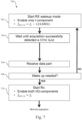
- Fig. 7 shows an illustrative embodiment of a second procedure 700 for operating a receiver circuit.
- the receiver circuit operates in the real receiver mode (i.e., using only the I-channel or I-component) until a signal is successfully acquired.
- this is implemented in the following manner.
- the receiver circuit is started in a wake-up mode, in which only the I-component is enabled, with a certain frequency offset, to detect the SYNC field for any phase offset between TX and RX. More specifically, the SYNC field of the first frame as well as the data part of the first frame is received.
- the controller waits until a SYNC field is detected.
- the successful acquisition of the signal may be based on the detection of a synchronization (SYNC) field within the signal.
- the data part of the first frame is received 706; this data part may indicate that a wake-up of the receiver circuit is needed.
- a wake-up is performed if indicated by the data part (e.g., a destination address matches, and a ranging exchange is started).
- the receiver circuit is started 710 and both the I-component and the Q-component may be enabled.
- the following frames are received with full receiver performance. This procedure is most suited for systems in which it is important that the receiver receives the payload of the first frame. For instance, in an access system the user may benefit from a fast response.
- energy is conserved, if the device only wakes up on frames that are intended for the device.
- Fig. 8A shows an illustrative embodiment of a third procedure 800 for operating a receiver circuit.
- the receiver circuit operates in the real receiver mode (i.e., using only the I-channel or I-component) until a signal is successfully acquired.
- this is implemented in the following manner.
- the receiver circuit is started in a wake-up mode, in which only the I-component is enabled, with a certain frequency offset, to detect the SYNC field for any phase offset between TX and RX.
- the controller waits until a SYNC field is detected.
- the successful acquisition of the signal may be based on the detection of a synchronization (SYNC) field within the signal.
- SYNC synchronization
- both the I-component and the Q-component are enabled.
- the wake-up is performed using only the I-component, but the data part of the first frame is received using both the I-component and the Q-component.
- the receiver circuit is started in a wake-up mode using only the I-component, however with immediate data reception using both quadrature branches.
- the Q-component is enabled immediately, such that the data part of the first frame is received 808 with both quadrature branches enabled and a nominal LO frequency offset.
- a full wake-up is performed if the data part indicates that a wake-up is needed 810 (e.g., a destination address matches, and a ranging exchange is started).
- the receiver circuit is started 812 and both the I-component and the Q-component may be enabled.
- the following frames are received with full receiver performance without a nominal LO frequency offset. This procedure is most suited for systems in which it is important that the receiver receives the payload of the first frame.
- the performance of the data reception is enhanced. This may be beneficial in an access system, in which the user benefits from a fast response. Furthermore, in a battery-powered application energy is conserved, if the device only wakes up on frames that are intended for the device.
- Fig. 8B shows an illustrative embodiment of a fourth procedure 814 for operating a receiver circuit.
- the receiver circuit operates in the real receiver mode (i.e., using only the I-channel or I-component) until a signal is successfully acquired.
- this is implemented in the following manner.
- the receiver circuit is started in a wake-up mode, in which only the I-component is enabled, with a certain frequency offset, to detect the SYNC field for any phase offset between TX and RX.
- the controller waits until a SYNC field is detected.
- the successful acquisition of the signal may be based on the detection of a synchronization (SYNC) field within the signal.
- SYNC synchronization
- both the I-component and the Q-component are enabled, and the center frequency is reset (i.e., changed back to its original value).
- changing back the center frequency at this point has the advantage that the data part of the first frame can be received with full sensitivity.
- the wake-up is performed using only the I-component, but the data part of the first frame is received using both the I-component and the Q-component. In this sense, it may be said that the receiver circuit is started in a wake-up mode using only the I-component, however with immediate data reception using both quadrature branches.
- the Q-component is enabled immediately, such that the data part of the first frame is received 808 with both quadrature branches enabled but without a nominal LO frequency offset.
- a full wake-up is performed if the data part indicates that a wake-up is needed 810 (e.g., a destination address matches, and a ranging exchange is started).
- the receiver circuit is started 812 and both the I-component and the Q-component may be enabled. Then, the following frames are received with full receiver performance without a nominal LO frequency offset.
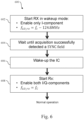
- Fig. 9 shows an illustrative embodiment of a fifth procedure 900 for operating a receiver circuit.
- the receiver circuit operates in the real receiver mode (i.e., using only the I-channel or I-component) until a signal is successfully acquired.
- this is implemented in the following manner.
- the receiver circuit is first started with full performance, i.e. with both the I-component and the Q-component enabled. If a signal is found within a certain time (i.e., a predefined amount of time), then the receiver circuit proceeds with its normal operation (i.e., regular operating mode).
- the UWB anchors receive scheduling information in the first UWB frame, it is important that this frame is properly received. Anchors that do not receive this scheduling information, should remain in a constant receive mode for considerable amounts of time (i.e., minutes or hours).
- the aforementioned wake-up mode may reduce the BOM and the size of the UWB module. It is noted that the BOM and size of a UWB anchor are to a large extent determined by the constant receive mode, because a DC/DC converter may be needed instead of a cheap linear regulator to reduce current consumption. Furthermore, a larger module with a lower thermal resistance may be needed to avoid overheating.
- the energy consumption is reduced by switching to the wake-up mode, if no signal is found within a certain time. Accordingly, the sensitivity of the receiver circuit may be traded off against the BOM, size and energy consumption of the receiver circuit.
Landscapes
- Engineering & Computer Science (AREA)
- Computer Networks & Wireless Communication (AREA)
- Signal Processing (AREA)
- Circuits Of Receivers In General (AREA)
Claims (9)
- Kommunikationsvorrichtung (100), umfassend:- eine Empfängerschaltung (102), ausgelegt zum Empfangen eines Signals, wobei das Signal ein Ultrabreitband- bzw. UWB-Pulssignal ist;- eine Steuerung (104), ausgelegt zum Steuern der Empfängerschaltung (102), wobei die Steuerung (104) dazu ausgelegt ist, zu bewirken, dass die Empfängerschaltung (102) entweder in einem komplexen Empfängermodus oder in einem realen Empfängermodus arbeitet;wobei die Steuerung (104) dazu ausgelegt ist, zu bewirken, dass die Empfängerschaltung (102) im realen Empfängermodus arbeitet, bis das Signal erfolgreich erfasst wurde;dadurch gekennzeichnet, dass die Steuerung (104) ferner dazu ausgelegt ist, zu bewirken, dass die Empfängerschaltung (102) im komplexen Empfängermodus einen I-Kanal und einen Q-Kanal des empfangenen Signals verwendet;wobei die Steuerung (104) ferner dazu ausgelegt ist, zu bewirken, dass die Empfängerschaltung (102) im realen Empfängermodus nur den I-Kanal des empfangenen Signals oder nur den Q-Kanal des empfangenen Signals verwendet;wobei die Steuerung (104) ferner dazu ausgelegt ist, wenn die Empfängerschaltung (102) im realen Empfängermodus arbeitet, eine Lokaloszillatorfrequenz anzuwenden, die sich von der Lokaloszillatorfrequenz unterscheidet, die angewendet wird, wenn die Empfängerschaltung (104) im komplexen Empfängermodus arbeitet, und wobei die Steuerung (104) dazu ausgelegt ist, wenn die Empfängerschaltung (102) im realen Empfängermodus arbeitet, die Lokaloszillatorfrequenz der Empfängerschaltung (102) um einen Bruchteil der Pulsrate zu versetzen.
- Vorrichtung (100) nach dem vorhergehenden Anspruch, wobei die Steuerung (104) ferner dazu ausgelegt ist, die Empfängerschaltung (102) bei oder nach einer erfolgreichen Erfassung des Signals von dem realen Empfängermodus in den komplexen Empfängermodus umzuschalten.
- Vorrichtung (100) nach Anspruch 2, wobei die erfolgreiche Erfassung des Signals auf der Detektion eines Synchronisationsfelds innerhalb des Signals basiert, wobei das Synchronisationsfeld in einem Datenframe enthalten ist.
- Vorrichtung (100) nach Anspruch 2 oder 3, wobei die Steuerung (104) ferner dazu ausgelegt ist, die Empfängerschaltung (102) aufzuwecken, bevor die Empfängerschaltung (102) von dem realen Empfängermodus in den komplexen Empfängermodus umgeschaltet wird.
- Vorrichtung (100) nach Anspruch 2 oder 3, wobei die Steuerung (104) ferner dazu ausgelegt ist, die Empfängerschaltung (102) aufzuwecken, nachdem die Empfängerschaltung (102) von dem realen Empfängermodus in den komplexen Empfängermodus umgeschaltet wird.
- Vorrichtung (100) nach einem der Ansprüche 2 bis 5, wobei die Steuerung (104) ferner dazu ausgelegt ist, eine Mittenfrequenz bei oder nach dem Umschalten der Empfängerschaltung (102) von dem realen Empfängermodus in den komplexen Empfängermodus zurückzusetzen.
- Vorrichtung (100) nach einem der vorhergehenden Ansprüche, wobei die Empfängerschaltung (102) dazu ausgelegt ist, standardmäßig im komplexen Empfängermodus zu arbeiten, und wobei die Steuerung (104) dazu ausgelegt ist, die Empfängerschaltung (102) von dem komplexen Empfängermodus in den realen Empfängermodus umzuschalten, wenn innerhalb einer vordefinierten Zeitdauer nach dem Starten der Empfängerschaltung (102) kein Signal gefunden wird.
- Vorrichtung (100) nach einem der vorhergehenden Ansprüche, bei der es sich um einen Ultrabreitband- bzw. UWB- Kommunikationsknoten handelt, der als ein Responder in einem Kommunikationssystem fungiert.
- Verfahren (200) zum Betreiben einer Kommunikationsvorrichtung, wobei die Kommunikationsvorrichtung eine Empfängerschaltung und eine Steuerung umfasst, wobei das Verfahren Folgendes umfasst:Empfangen (202), durch die Empfängerschaltung, eines Signals, wobei das Signal ein Ultrabreitband- bzw. UWB-Pulssignal ist;Steuern (204), durch die Steuerung, der Empfängerschaltung;wobei die Steuerung bewirkt, dass die Empfängerschaltung entweder in einem komplexen Empfängermodus oder in einem realen Empfängermodus arbeitet;wobei die Steuerung bewirkt, dass die Empfängerschaltung im realen Empfängermodus arbeitet, bis das Signal erfolgreich erfasst wurde;dadurch gekennzeichnet, dass die Steuerung bewirkt, dass die Empfängerschaltung im komplexen Empfängermodus einen I-Kanal und einen Q-Kanal des empfangenen Signals verwendet;wobei die Steuerung bewirkt, dass die Empfängerschaltung im realen Empfängermodus nur den I-Kanal des empfangenen Signals oder nur den Q-Kanal des empfangenen Signals verwendet;wobei die Steuerung, wenn die Empfängerschaltung im realen Empfängermodus arbeitet, eine Lokaloszillatorfrequenz anwendet, die sich von der Lokaloszillatorfrequenz unterscheidet, die angewendet wird, wenn der Empfänger im komplexen Empfängermodus arbeitet, und wobei die Steuerung dazu ausgelegt ist, wenn die Empfängerschaltung im realen Empfängermodus arbeitet, die Lokaloszillatorfrequenz der Empfängerschaltung um einen Bruchteil der Pulsrate zu versetzen.
Priority Applications (3)
| Application Number | Priority Date | Filing Date | Title |
|---|---|---|---|
| EP21201236.3A EP4164134B1 (de) | 2021-10-06 | 2021-10-06 | Kommunikationsvorrichtung und betriebsverfahren |
| US17/929,181 US12113571B2 (en) | 2021-10-06 | 2022-09-01 | Communication device and operating method |
| CN202211140507.8A CN115940975A (zh) | 2021-10-06 | 2022-09-19 | 通信装置和操作方法 |
Applications Claiming Priority (1)
| Application Number | Priority Date | Filing Date | Title |
|---|---|---|---|
| EP21201236.3A EP4164134B1 (de) | 2021-10-06 | 2021-10-06 | Kommunikationsvorrichtung und betriebsverfahren |
Publications (2)
| Publication Number | Publication Date |
|---|---|
| EP4164134A1 EP4164134A1 (de) | 2023-04-12 |
| EP4164134B1 true EP4164134B1 (de) | 2025-07-02 |
Family
ID=78332475
Family Applications (1)
| Application Number | Title | Priority Date | Filing Date |
|---|---|---|---|
| EP21201236.3A Active EP4164134B1 (de) | 2021-10-06 | 2021-10-06 | Kommunikationsvorrichtung und betriebsverfahren |
Country Status (3)
| Country | Link |
|---|---|
| US (1) | US12113571B2 (de) |
| EP (1) | EP4164134B1 (de) |
| CN (1) | CN115940975A (de) |
Families Citing this family (1)
| Publication number | Priority date | Publication date | Assignee | Title |
|---|---|---|---|---|
| FR3139692B1 (fr) * | 2022-09-08 | 2024-09-13 | St Microelectronics Rousset | Appareil de communication sans fil configuré pour communiquer en ultra large bande |
Family Cites Families (7)
| Publication number | Priority date | Publication date | Assignee | Title |
|---|---|---|---|---|
| US6055556A (en) * | 1997-08-15 | 2000-04-25 | Motorola, Inc. | Apparatus and method for matrix multiplication |
| US7362826B2 (en) * | 2003-09-29 | 2008-04-22 | Silicon Laboratories, Inc. | Receiver including an oscillation circuit for generating an image rejection calibration tone |
| EP3355478B1 (de) * | 2014-09-10 | 2019-08-07 | Telefonaktiebolaget LM Ericsson (publ) | Funkempfänger für trägeraggregation |
| US11051244B2 (en) * | 2019-05-31 | 2021-06-29 | Nxp B.V. | Ultra-wideband (UWB) receiver device and method for operating a UWB device |
| EP3978948A1 (de) * | 2020-10-05 | 2022-04-06 | NXP USA, Inc. | Radargerät und entsprechendes betriebsverfahren |
| US11750235B2 (en) * | 2021-06-24 | 2023-09-05 | Analog Devices International Unlimited Company | Radio frequency receiver circuit |
| EP4137836B1 (de) * | 2021-08-20 | 2025-07-02 | Nxp B.V. | Kommunikationsvorrichtung und entsprechendes betriebsverfahren |
-
2021
- 2021-10-06 EP EP21201236.3A patent/EP4164134B1/de active Active
-
2022
- 2022-09-01 US US17/929,181 patent/US12113571B2/en active Active
- 2022-09-19 CN CN202211140507.8A patent/CN115940975A/zh active Pending
Also Published As
| Publication number | Publication date |
|---|---|
| EP4164134A1 (de) | 2023-04-12 |
| US20230108844A1 (en) | 2023-04-06 |
| US12113571B2 (en) | 2024-10-08 |
| CN115940975A (zh) | 2023-04-07 |
Similar Documents
| Publication | Publication Date | Title |
|---|---|---|
| US10292104B2 (en) | Quick decision preamble detector with hierarchical processing | |
| US7369485B2 (en) | Wireless receiver for sorting packets | |
| US8301208B2 (en) | Receiver and receiving method of the receiver | |
| US20120281740A1 (en) | Transmitting apparatus, receiving apparatus and communication system | |
| KR100665374B1 (ko) | 대역 확산 기법을 적용한 위치인식용 카오스 무선통신 장치 | |
| US11611360B2 (en) | Apparatus for receiver with concurrent detection and associated methods | |
| US8755461B2 (en) | Local wireless signal transmitting/receiving apparatus and method using digital radio frequency processing technology | |
| US8457176B2 (en) | Fast frequency-hopping transceiver and method | |
| JP4900754B2 (ja) | アナログ相関を用いたデジタル受信機感度拡張方法 | |
| US20100220774A1 (en) | Low power uwb transmitter and receiver in impulse-based uwb communication system and method for operating the same | |
| EP4164134B1 (de) | Kommunikationsvorrichtung und betriebsverfahren | |
| US11051244B2 (en) | Ultra-wideband (UWB) receiver device and method for operating a UWB device | |
| Barras et al. | A low-power baseband ASIC for an energy-collection IR-UWB receiver | |
| JP2006050333A (ja) | 無線受信装置 | |
| EP4046280B1 (de) | Überabgetastete mehrfachkorrelatorsymbolsynchronisation | |
| US20250379610A1 (en) | Duty-cycle-based receiver with listening power consumption reduction | |
| JP2007504720A (ja) | 無線ネットワークデバイスにおけるエネルギー効率の良い信号検出のためのシステム及び方法 | |
| US12592788B2 (en) | Wake-up radio having single bit correlators | |
| KR20070046960A (ko) | 무선 장치 및 배터리 수명 연장 방법 | |
| US20240187036A1 (en) | Signal identification for multi-channel and multi-protocol communications | |
| CN118574199A (zh) | 具有单比特相关器的唤醒无线电 | |
| US20250189651A1 (en) | Systems, methods, and devices for radar operation in wireless devices | |
| JP2009159168A (ja) | 無線受信機 | |
| JP2015170890A (ja) | 無線通信装置及び無線通信方法 | |
| JP2016103721A (ja) | 受信装置 |
Legal Events
| Date | Code | Title | Description |
|---|---|---|---|
| PUAI | Public reference made under article 153(3) epc to a published international application that has entered the european phase |
Free format text: ORIGINAL CODE: 0009012 |
|
| STAA | Information on the status of an ep patent application or granted ep patent |
Free format text: STATUS: THE APPLICATION HAS BEEN PUBLISHED |
|
| AK | Designated contracting states |
Kind code of ref document: A1 Designated state(s): AL AT BE BG CH CY CZ DE DK EE ES FI FR GB GR HR HU IE IS IT LI LT LU LV MC MK MT NL NO PL PT RO RS SE SI SK SM TR |
|
| STAA | Information on the status of an ep patent application or granted ep patent |
Free format text: STATUS: REQUEST FOR EXAMINATION WAS MADE |
|
| 17P | Request for examination filed |
Effective date: 20231012 |
|
| RBV | Designated contracting states (corrected) |
Designated state(s): AL AT BE BG CH CY CZ DE DK EE ES FI FR GB GR HR HU IE IS IT LI LT LU LV MC MK MT NL NO PL PT RO RS SE SI SK SM TR |
|
| GRAP | Despatch of communication of intention to grant a patent |
Free format text: ORIGINAL CODE: EPIDOSNIGR1 |
|
| STAA | Information on the status of an ep patent application or granted ep patent |
Free format text: STATUS: GRANT OF PATENT IS INTENDED |
|
| RIC1 | Information provided on ipc code assigned before grant |
Ipc: H04B 1/7163 20110101ALI20250331BHEP Ipc: H04B 1/7183 20110101AFI20250331BHEP |
|
| INTG | Intention to grant announced |
Effective date: 20250410 |
|
| GRAS | Grant fee paid |
Free format text: ORIGINAL CODE: EPIDOSNIGR3 |
|
| GRAA | (expected) grant |
Free format text: ORIGINAL CODE: 0009210 |
|
| STAA | Information on the status of an ep patent application or granted ep patent |
Free format text: STATUS: THE PATENT HAS BEEN GRANTED |
|
| AK | Designated contracting states |
Kind code of ref document: B1 Designated state(s): AL AT BE BG CH CY CZ DE DK EE ES FI FR GB GR HR HU IE IS IT LI LT LU LV MC MK MT NL NO PL PT RO RS SE SI SK SM TR |
|
| REG | Reference to a national code |
Ref country code: GB Ref legal event code: FG4D |
|
| REG | Reference to a national code |
Ref country code: CH Ref legal event code: EP |
|
| REG | Reference to a national code |
Ref country code: DE Ref legal event code: R096 Ref document number: 602021033239 Country of ref document: DE |
|
| REG | Reference to a national code |
Ref country code: IE Ref legal event code: FG4D |
|
| PGFP | Annual fee paid to national office [announced via postgrant information from national office to epo] |
Ref country code: FR Payment date: 20250923 Year of fee payment: 5 |
|
| REG | Reference to a national code |
Ref country code: NL Ref legal event code: MP Effective date: 20250702 |
|
| PG25 | Lapsed in a contracting state [announced via postgrant information from national office to epo] |
Ref country code: PT Free format text: LAPSE BECAUSE OF FAILURE TO SUBMIT A TRANSLATION OF THE DESCRIPTION OR TO PAY THE FEE WITHIN THE PRESCRIBED TIME-LIMIT Effective date: 20251103 |
|
| PG25 | Lapsed in a contracting state [announced via postgrant information from national office to epo] |
Ref country code: NL Free format text: LAPSE BECAUSE OF FAILURE TO SUBMIT A TRANSLATION OF THE DESCRIPTION OR TO PAY THE FEE WITHIN THE PRESCRIBED TIME-LIMIT Effective date: 20250702 |
|
| REG | Reference to a national code |
Ref country code: AT Ref legal event code: MK05 Ref document number: 1810465 Country of ref document: AT Kind code of ref document: T Effective date: 20250702 |
|
| PG25 | Lapsed in a contracting state [announced via postgrant information from national office to epo] |
Ref country code: IS Free format text: LAPSE BECAUSE OF FAILURE TO SUBMIT A TRANSLATION OF THE DESCRIPTION OR TO PAY THE FEE WITHIN THE PRESCRIBED TIME-LIMIT Effective date: 20251102 |
|
| PGFP | Annual fee paid to national office [announced via postgrant information from national office to epo] |
Ref country code: DE Payment date: 20250923 Year of fee payment: 5 |
|
| PG25 | Lapsed in a contracting state [announced via postgrant information from national office to epo] |
Ref country code: NO Free format text: LAPSE BECAUSE OF FAILURE TO SUBMIT A TRANSLATION OF THE DESCRIPTION OR TO PAY THE FEE WITHIN THE PRESCRIBED TIME-LIMIT Effective date: 20251002 |
|
| REG | Reference to a national code |
Ref country code: LT Ref legal event code: MG9D |
|
| PG25 | Lapsed in a contracting state [announced via postgrant information from national office to epo] |
Ref country code: AT Free format text: LAPSE BECAUSE OF FAILURE TO SUBMIT A TRANSLATION OF THE DESCRIPTION OR TO PAY THE FEE WITHIN THE PRESCRIBED TIME-LIMIT Effective date: 20250702 |
|
| PG25 | Lapsed in a contracting state [announced via postgrant information from national office to epo] |
Ref country code: FI Free format text: LAPSE BECAUSE OF FAILURE TO SUBMIT A TRANSLATION OF THE DESCRIPTION OR TO PAY THE FEE WITHIN THE PRESCRIBED TIME-LIMIT Effective date: 20250702 |
|
| PG25 | Lapsed in a contracting state [announced via postgrant information from national office to epo] |
Ref country code: HR Free format text: LAPSE BECAUSE OF FAILURE TO SUBMIT A TRANSLATION OF THE DESCRIPTION OR TO PAY THE FEE WITHIN THE PRESCRIBED TIME-LIMIT Effective date: 20250702 |
|
| PG25 | Lapsed in a contracting state [announced via postgrant information from national office to epo] |
Ref country code: GR Free format text: LAPSE BECAUSE OF FAILURE TO SUBMIT A TRANSLATION OF THE DESCRIPTION OR TO PAY THE FEE WITHIN THE PRESCRIBED TIME-LIMIT Effective date: 20251003 |
|
| PG25 | Lapsed in a contracting state [announced via postgrant information from national office to epo] |
Ref country code: CZ Free format text: LAPSE BECAUSE OF FAILURE TO SUBMIT A TRANSLATION OF THE DESCRIPTION OR TO PAY THE FEE WITHIN THE PRESCRIBED TIME-LIMIT Effective date: 20250702 Ref country code: SE Free format text: LAPSE BECAUSE OF FAILURE TO SUBMIT A TRANSLATION OF THE DESCRIPTION OR TO PAY THE FEE WITHIN THE PRESCRIBED TIME-LIMIT Effective date: 20250702 |
|
| PG25 | Lapsed in a contracting state [announced via postgrant information from national office to epo] |
Ref country code: LV Free format text: LAPSE BECAUSE OF FAILURE TO SUBMIT A TRANSLATION OF THE DESCRIPTION OR TO PAY THE FEE WITHIN THE PRESCRIBED TIME-LIMIT Effective date: 20250702 |
|
| PG25 | Lapsed in a contracting state [announced via postgrant information from national office to epo] |
Ref country code: BG Free format text: LAPSE BECAUSE OF FAILURE TO SUBMIT A TRANSLATION OF THE DESCRIPTION OR TO PAY THE FEE WITHIN THE PRESCRIBED TIME-LIMIT Effective date: 20250702 Ref country code: PL Free format text: LAPSE BECAUSE OF FAILURE TO SUBMIT A TRANSLATION OF THE DESCRIPTION OR TO PAY THE FEE WITHIN THE PRESCRIBED TIME-LIMIT Effective date: 20250702 |
|
| PG25 | Lapsed in a contracting state [announced via postgrant information from national office to epo] |
Ref country code: RS Free format text: LAPSE BECAUSE OF FAILURE TO SUBMIT A TRANSLATION OF THE DESCRIPTION OR TO PAY THE FEE WITHIN THE PRESCRIBED TIME-LIMIT Effective date: 20251002 |
|
| PG25 | Lapsed in a contracting state [announced via postgrant information from national office to epo] |
Ref country code: ES Free format text: LAPSE BECAUSE OF FAILURE TO SUBMIT A TRANSLATION OF THE DESCRIPTION OR TO PAY THE FEE WITHIN THE PRESCRIBED TIME-LIMIT Effective date: 20250702 |
|
| PG25 | Lapsed in a contracting state [announced via postgrant information from national office to epo] |
Ref country code: RO Free format text: LAPSE BECAUSE OF FAILURE TO SUBMIT A TRANSLATION OF THE DESCRIPTION OR TO PAY THE FEE WITHIN THE PRESCRIBED TIME-LIMIT Effective date: 20250702 |
|
| PG25 | Lapsed in a contracting state [announced via postgrant information from national office to epo] |
Ref country code: SM Free format text: LAPSE BECAUSE OF FAILURE TO SUBMIT A TRANSLATION OF THE DESCRIPTION OR TO PAY THE FEE WITHIN THE PRESCRIBED TIME-LIMIT Effective date: 20250702 |
|
| PG25 | Lapsed in a contracting state [announced via postgrant information from national office to epo] |
Ref country code: DK Free format text: LAPSE BECAUSE OF FAILURE TO SUBMIT A TRANSLATION OF THE DESCRIPTION OR TO PAY THE FEE WITHIN THE PRESCRIBED TIME-LIMIT Effective date: 20250702 |
|
| PG25 | Lapsed in a contracting state [announced via postgrant information from national office to epo] |
Ref country code: IT Free format text: LAPSE BECAUSE OF FAILURE TO SUBMIT A TRANSLATION OF THE DESCRIPTION OR TO PAY THE FEE WITHIN THE PRESCRIBED TIME-LIMIT Effective date: 20250702 |