EP3355478B1 - Funkempfänger für trägeraggregation - Google Patents
Funkempfänger für trägeraggregation Download PDFInfo
- Publication number
- EP3355478B1 EP3355478B1 EP18154125.1A EP18154125A EP3355478B1 EP 3355478 B1 EP3355478 B1 EP 3355478B1 EP 18154125 A EP18154125 A EP 18154125A EP 3355478 B1 EP3355478 B1 EP 3355478B1
- Authority
- EP
- European Patent Office
- Prior art keywords
- direct conversion
- receive path
- conversion receiver
- signal
- mode
- Prior art date
- Legal status (The legal status is an assumption and is not a legal conclusion. Google has not performed a legal analysis and makes no representation as to the accuracy of the status listed.)
- Active
Links
- 238000004220 aggregation Methods 0.000 title claims description 16
- 230000002776 aggregation Effects 0.000 title description 8
- 238000012545 processing Methods 0.000 claims description 46
- 238000000034 method Methods 0.000 claims description 42
- 238000006243 chemical reaction Methods 0.000 claims description 40
- 238000005259 measurement Methods 0.000 claims description 32
- 238000004891 communication Methods 0.000 claims description 20
- 230000010267 cellular communication Effects 0.000 claims description 18
- 230000008569 process Effects 0.000 claims description 14
- 239000000969 carrier Substances 0.000 claims description 10
- 238000004590 computer program Methods 0.000 description 15
- 238000010586 diagram Methods 0.000 description 6
- 238000001914 filtration Methods 0.000 description 4
- 238000013461 design Methods 0.000 description 3
- 230000000903 blocking effect Effects 0.000 description 2
- 238000004422 calculation algorithm Methods 0.000 description 2
- 230000015556 catabolic process Effects 0.000 description 2
- 230000008859 change Effects 0.000 description 2
- 230000003247 decreasing effect Effects 0.000 description 2
- 238000006731 degradation reaction Methods 0.000 description 2
- 238000001514 detection method Methods 0.000 description 2
- 230000006872 improvement Effects 0.000 description 2
- 238000003491 array Methods 0.000 description 1
- 230000009286 beneficial effect Effects 0.000 description 1
- 230000005540 biological transmission Effects 0.000 description 1
- 238000004364 calculation method Methods 0.000 description 1
- 230000001413 cellular effect Effects 0.000 description 1
- 230000001419 dependent effect Effects 0.000 description 1
- 230000010363 phase shift Effects 0.000 description 1
- 230000000630 rising effect Effects 0.000 description 1
- 238000009738 saturating Methods 0.000 description 1
- 230000008054 signal transmission Effects 0.000 description 1
- 230000001629 suppression Effects 0.000 description 1
- 230000002194 synthesizing effect Effects 0.000 description 1
Images


Classifications
-
- H—ELECTRICITY
- H03—ELECTRONIC CIRCUITRY
- H03D—DEMODULATION OR TRANSFERENCE OF MODULATION FROM ONE CARRIER TO ANOTHER
- H03D7/00—Transference of modulation from one carrier to another, e.g. frequency-changing
- H03D7/14—Balanced arrangements
- H03D7/1425—Balanced arrangements with transistors
- H03D7/1466—Passive mixer arrangements
-
- H—ELECTRICITY
- H04—ELECTRIC COMMUNICATION TECHNIQUE
- H04B—TRANSMISSION
- H04B1/00—Details of transmission systems, not covered by a single one of groups H04B3/00 - H04B13/00; Details of transmission systems not characterised by the medium used for transmission
- H04B1/005—Details of transmission systems, not covered by a single one of groups H04B3/00 - H04B13/00; Details of transmission systems not characterised by the medium used for transmission adapting radio receivers, transmitters andtransceivers for operation on two or more bands, i.e. frequency ranges
- H04B1/0053—Details of transmission systems, not covered by a single one of groups H04B3/00 - H04B13/00; Details of transmission systems not characterised by the medium used for transmission adapting radio receivers, transmitters andtransceivers for operation on two or more bands, i.e. frequency ranges with common antenna for more than one band
-
- H—ELECTRICITY
- H04—ELECTRIC COMMUNICATION TECHNIQUE
- H04B—TRANSMISSION
- H04B1/00—Details of transmission systems, not covered by a single one of groups H04B3/00 - H04B13/00; Details of transmission systems not characterised by the medium used for transmission
- H04B1/005—Details of transmission systems, not covered by a single one of groups H04B3/00 - H04B13/00; Details of transmission systems not characterised by the medium used for transmission adapting radio receivers, transmitters andtransceivers for operation on two or more bands, i.e. frequency ranges
- H04B1/0067—Details of transmission systems, not covered by a single one of groups H04B3/00 - H04B13/00; Details of transmission systems not characterised by the medium used for transmission adapting radio receivers, transmitters andtransceivers for operation on two or more bands, i.e. frequency ranges with one or more circuit blocks in common for different bands
-
- H—ELECTRICITY
- H04—ELECTRIC COMMUNICATION TECHNIQUE
- H04L—TRANSMISSION OF DIGITAL INFORMATION, e.g. TELEGRAPHIC COMMUNICATION
- H04L27/00—Modulated-carrier systems
- H04L27/26—Systems using multi-frequency codes
- H04L27/2601—Multicarrier modulation systems
- H04L27/2647—Arrangements specific to the receiver only
-
- H—ELECTRICITY
- H04—ELECTRIC COMMUNICATION TECHNIQUE
- H04L—TRANSMISSION OF DIGITAL INFORMATION, e.g. TELEGRAPHIC COMMUNICATION
- H04L5/00—Arrangements affording multiple use of the transmission path
- H04L5/0001—Arrangements for dividing the transmission path
- H04L5/0003—Two-dimensional division
- H04L5/0005—Time-frequency
- H04L5/0007—Time-frequency the frequencies being orthogonal, e.g. OFDM(A) or DMT
- H04L5/001—Time-frequency the frequencies being orthogonal, e.g. OFDM(A) or DMT the frequencies being arranged in component carriers
Definitions
- the present invention relates to radio receiver circuits capable of operation in carrier-aggregation scenarios.
- wireless terminals In cellular communications networks, wireless terminals, sometimes referred to as UEs (User Equipment), communicate wirelessly with base stations of the cellular communications network.
- the UE In the downlink, from the base station to the UE, the UE may receive signals in a single frequency band associated with a single radio-frequency (RF) carrier.
- RF radio-frequency
- CA carrier aggregation
- the concept of carrier aggregation (CA) has been introduced in 3GPP (3rd Generation Partnership Program) standards.
- CA carrier aggregation
- the UE may simultaneously receive a plurality of RF carriers. These RF carriers are normally referred to as component carriers, or CCs. On each CC there is modulated an information signal, e.g.
- the CCs may be located within the same operating frequency band, in which case the CA is referred to as intra-band CA. Alternatively, the CCs may be located within different operating frequency bands, in which case the CA is referred to as inter-band CA.
- the plurality of CCs may be located contiguously (in frequency), in which case the CA is referred to as contiguous CA, or may be non-contiguously located (in frequency) with frequency gaps in between, in which case the CA is referred to as non-contiguous CA.
- the UE may be allocated a primary CC (PCC) associated with a primary cell (PCell) of the cellular communications network.
- PCC primary CC
- PCell primary cell
- SCells secondary CCs
- Each receive path may be responsible for reception of a particular one of the plurality of CCs.
- each receive path may be of direct-conversion type, comprising a mixer unit driven by an LO signal having a frequency selected such that the mixer unit directly down-converts the particular CC to base band.
- the LO-signal frequency of each processing path may thus be selected in dependence of the RF frequency of the CC it is set to receive.
- Embodiments of the present invention are based on an insight that receiver circuitry intended for CA operation may be efficiently reused in non-CA (or "single carrier") operation for boosting the performance.
- a radio receiver circuit configurable to operate in a CA mode, wherein the radio receiver circuit is to receive a plurality of component carriers (CCs), and in a non-CA mode, wherein the radio receiver circuit is to receive a single CC.
- the radio receiver circuit comprises a first receive path arranged to be operatively connected to an antenna and a second receive path arranged to be operatively connected to the same antenna.
- the radio receiver circuit comprises a control unit operatively connected to the first receive path and the second receive path.
- the control unit is adapted to, in the CA mode, control the first receive path to receive a first CC of said plurality of CCs and control the second receive path to receive a second CC, separate from the first CC, of said plurality of CCs. Moreover, the control unit is adapted to, in the non-CA mode, selectively control the first receive path and the second receive path to both receive the same single CC.
- the radio receiver circuit may comprise a low-noise amplifier arranged to operatively connect both the first receive path and the second receive path to the antenna.
- the first receive path may comprise a mixer unit arranged to be driven by a first local oscillator (LO) signal.
- the second receive path may comprise a mixer unit arranged to be driven by a second LO signal.
- the control unit may be adapted to, in the CA mode, control the frequency of the first LO signal to enable reception of the first CC by the first receive path and control the frequency of the second LO signal to enable reception of the second CC by the second receive path.
- the control unit may be adapted to, in the non-CA mode and in order to enable reception of the same single CC by both the first receive path and the second receive path, control the frequency of the first LO signal to be the same as the frequency of the second LO signal.
- the radio receiver circuit may comprise processing circuitry arranged to, in the non-CA mode, combine an output signal of the first receive path with an output signal of the second receive path, thereby generating a combined output signal.
- the control unit may be adapted to, in the non-CA mode, control at least one of a gain and a frequency bandwidth of the first receive path to be the same as that of the second receive path when the first receive path and the second receive path are controlled to both receive the same signal in said single frequency band
- the radio receiver circuit may comprise processing circuitry arranged to, in the non-CA mode, separately process an output signal of the first receive path and an output signal of the second receive path, thereby generating a first processed signal and a second processed signal, respectively.
- the control unit may be adapted to, in the non-CA mode, control a gain of one of the first receive path and the second receive path to be higher than a gain of the other one of the first receive path and the second receive path when the first receive path and the second receive path are controlled to both receive the same single CC.
- the processing circuitry may be arranged to perform signal-strength measurements on the output signal from the first receive path and on the output signal from the second receive path, for example to determine a gain setting to be used during further reception in the non-CA mode.
- the control unit may be adapted to, in the non-CA mode, selectively disable the second receive path.
- the radio receiver circuit may be adapted to operate in a cellular communication system.
- a radio communication apparatus comprising a radio receiver circuit according to the first aspect and an antenna, to which both the first receive path and the second receive path of the radio receiver circuit are operatively connected.
- the radio communication apparatus may be a terminal for a cellular communication system.
- the terminal may for example be a mobile telephone, a tablet computer, a portable computer, or a machine-type communication device.
- a method of operating a radio receiver circuit configurable to operate in a CA mode, wherein the radio receiver circuit is to receive a plurality of component carriers (CCs), and in a non-CA mode, wherein the radio receiver circuit is to receive a single CC.
- the radio receiver circuit comprises a first receive path operatively connected to an antenna, a second receive path operatively connected to the same antenna, and a control unit operatively connected to the first receive path and the second receive path.
- the method comprises controlling, in the CA mode and by the control unit, the first receive path to receive a first CC of said plurality of CCs and the second receive path to receive a second CC, separate from the first CC, of said plurality of CCs.
- the method comprises selectively controlling, in the non-CA mode and by the control unit, the first receive path and the second receive path to both receive the same single CC.
- a computer program product comprising computer program code for executing the method according to the third aspect when said computer program code is executed by the control unit of the radio receiver circuit
- a computer readable medium (such as a non-transitory computer readable medium) having stored thereon a computer program product comprising computer program code for executing the method according to the third aspect when said computer program code is executed by the control unit of the radio receiver circuit.
- the computer readable medium may e.g. be a non-transitory computer readable medium.
- WO 2012/109262 discloses a multi-band user equipment (UE) that is configured to operate in a single frequency band mode (non carrier aggregation mode) or a multiple frequency band mode (carrier aggregation mode).
- UE user equipment
- the UE activates a bypass switch to route uplink signals of a first band around a multiplexer.
- US2013/051284 discloses a system with two antennas: one connected to a main receiver and the second one (diversity antenna) connected to a diversity receiver.
- the second antenna is also connected to a carrier aggregation receiver.
- mode 1 non carrier-aggregation mode
- the main receiver with the first antenna and the diversity receiver with the second antenna are used.
- mode 2 carrier aggregation mode
- the diversity antenna is used to receive the second carrier.
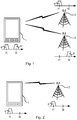
- FIGS. 1 and 2 illustrate communication environments wherein embodiments of the present invention may be employed.
- a radio-communication apparatus 1 illustrated as a terminal 1 for a cellular communication system, is in wireless communication with a cellular communication system in a carrier aggregation (CA) mode.
- the terminal 1 is depicted as a mobile telephone (or "cellular telephone", such as a so called smartphone), but it can also be any other type of terminal for a cellular communication system, such as a tablet computer, a portable computer, or a machine-type communication device (e.g. a sensor, sensor system, or similar arranged to communicate via a cellular communication system).
- the radio-communication apparatus 1 is in the following referred to as "the terminal 1".
- a radio-receiver circuit (further described below) of the terminal 1 is arranged to receive a plurality of (downlink) component carriers (CCs), which may be contiguous or non-contiguous.
- CCs downlink component carriers
- one of the CCs is a PCC of a PCell (described in the background section above), and the other CCs are SCCs of SCells (also described in the background section above).
- the plurality of CCs comprises a first frequency CC 6 at a first (RF) carrier frequency f1 and a second CC 8, which is separate from the first CC 6, at a second (RF) carrier frequency f2.
- the first CC 6 may e.g.
- the PCC may be the PCC
- the second CC 8 may e.g. be an SCC, or vice versa.
- there may be more than one SCell there may be more than two CCs in the plurality of CCs.
- the first CC 6 is illustrated as transmitted from a first base station 2
- the second CC 8 is illustrated as transmitted from a second base station 3, but in general they may also be transmitted from the same base station.
- the base station or base stations 2, 3 may e.g.
- the first and second CCs 6,8 are illustrated as non-contiguous (or non-adjacent) CCs having a frequency gap between them, but in other embodiments or scenarios, they may be contiguous (or adjacent) CCs.
- the terminal 1 is in wireless communication with the cellular communication system in a non-CA mode.
- the radio receiver circuit of the terminal 1 is arranged to receive a single CC.
- the single CC is illustrated as the same CC as the first CC 6 from the first base station 2 in Fig. 1 , but may well be some other CC (such as but not limited to the second CC 8 in Fig. 1 ) and/or from some other base station (such as but not limited to the second base station 3 in Fig. 1 ).
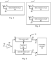
- Fig. 3 shows a simplified block diagram of a part of the terminal 1 according to an embodiment.
- the above-mentioned radio receiver circuit is denoted with reference number 10. It is operatively connected to an antenna 15 of the terminal 10 via an antenna port 20 of the radio receiver circuit 10.
- the terminal 1 may naturally also comprise many other parts as well, such as one or more transmitters, one or more processors, input and output devices (e.g. buttons, displays, touchscreens, etc), etc. For simplicity, such other parts are not shown in Fig. 3 .
- the terminal 1 is illustrated as having a single antenna 15. In other embodiments, the terminal 1 may have multiple antennas. For example, the terminal 1 may have multiple receive antennas for diversity reception.
- Fig. 4 shows a simplified block diagram of another embodiment of the terminal 1.
- the embodiment of the terminal 1 in Fig. 4 comprises the radio receiver circuit 10 operatively connected to the antenna 15 of the terminal 1 via the antenna port 20 of the radio receiver circuit 10.
- the terminal 1 comprises another radio receiver circuit 10' and another antenna 15', wherein the radio receiver circuit 10' is operatively connected to the antenna 15' of the terminal 1 via an antenna port 20' of the radio receiver circuit 10'.
- the radio receiver circuit 10' may e.g. be designed in the same way as the radio receiver circuit 10.
- Fig. 5 shows a block diagram of an embodiment of the radio receiver circuit 10.
- the radio receiver circuit 10 is configurable to operate in a CA mode, wherein the radio receiver circuit 10 is to receive a plurality of CCs, such as the CCs 6 and 8 ( Fig. 1 ).
- the radio receiver circuit 10 is configurable to operate in a non-CA mode, wherein the radio receiver circuit 10 is to receive a single CC, such as the CC 6 ( Fig. 2 ).
- the radio receiver circuit 10 may for example be adapted to operate in a cellular communication system.
- the radio receiver circuit 10 comprises a first receive path 30 arranged to be operatively connected to the antenna.
- the first receive path 30 has an input port 32 arranged to be operatively connected to the antenna 15.
- the first receive path 30 has an output port 34 arranged to provide an output signal of the first receive path 30.
- the radio receiver circuit 10 comprises a second receive path 40 arranged to be operatively connected to the same antenna 15.
- the second receive path 40 has an input port 42 arranged to be operatively connected to the antenna 15.
- the second receive path 40 has an output port 44 arranged to provide an output signal of the second receive path 40.
- the radio receiver circuit 10 comprises an LNA (Low-Noise Amplifier) 60 common to the first receive path 30 and the second receive path 40.
- the LNA 60 is arranged to operatively connect both the first receive path 30 and the second receive path 40 to the antenna 15, via the antenna port 20 of the radio receiver circuit 10.
- the radio receiver circuit 10 may comprise separate LNAs arranged to operatively connect the first receive path 30 and the second receive path 40, respectively, to the antenna 15, via the antenna port 20 of the radio receiver circuit 10.
- the radio receiver circuit 10 further comprises a control unit 50 operatively connected to the first receive path 30 and the second receive path 40 for controlling the operation of the first receive path 30 and the second receive path 40.
- the radio receiver circuit 10 comprises processing circuitry 70 operatively connected to the first receive path 30 and the second receive path 40 and arranged to process the output signals from the first receive path 30 and the second receive path 40.
- the processing circuitry 70 may have an input port 72 connected to the output port 34 of the first receive path 30, and an input port 74 connected to the output port 44 of the second receive path 40.
- the processing circuitry 70 may for example comprise, be, or be part of a digital signal processor, such as a baseband processor of the radio receiver circuit 10.
- the control unit 50 may comprise, be, or be part of a digital signal processor, such as a baseband processor of the radio receiver circuit 10, potentially the same digital signal processor as for the processing circuitry 70 mentioned in the preceding sentence.
- the control unit 50 is adapted to, in the CA mode, control the first receive path 30 to receive a first CC 6 of said plurality of frequency bands and control the second receive path to receive a second CC 8 of said plurality of CCs.
- the processing circuitry 70 can then process the output signals from the first receive path 30 and the second receive path 40, e.g. according to well-known techniques, including for example demodulation and decoding of the output signals, to recover the data transmitted on the signals in the respective frequency bands.
- the control unit 50 is adapted to, in the non-CA mode, selectively control the first receive path 30 and the second receive path 40 to both receive the same single CC 6.
- the control unit 50 is adapted to, in the non-CA mode, selectively disable the second receive path 40.
- Fig. 6 is a block diagram of an embodiment of the radio receiver circuit 10, showing some more details than the block diagram in Fig. 5 .
- the first receive path 30 may comprise a mixer unit 100 arranged to be driven by a first local oscillator (LO) signal.
- the second receive path 40 may comprise a mixer unit 200 arranged to be driven by a second LO signal.
- the control unit 50 may be adapted to, in the CA mode, control the frequency of the first LO signal to enable reception of the first CC 6 by the first receive path 30 and control the frequency of the second LO signal to enable reception of the second CC 8 by the second receive path 40.
- the first LO signal and the second LO signal are distinct LO signals generated by distinct LO units.
- the first receive path 30 may comprise a LO unit 110 arranged to generate the first LO signal
- the second receive path 40 may comprise a separate LO unit 210 arranged to generate the second LO signal.
- the first receive path 30 and the second receive path 40 may then, for example, both operate as direct conversion receivers.
- the control unit 50 may be adapted to, in the CA mode, control the frequency of the first LO signal and the frequency of the second LO signal to be equal, or approximately equal, to the center frequency f1 of the first CC 6 and the center frequency f2 of the second CC 8, respectively.
- control unit 50 may be adapted to, in the non-CA mode, control the frequency of the first LO signal to be the same as the frequency of the second LO signal.
- This same frequency may, for instance, be equal, or approximately equal, to the center frequency f1 of the single CC 6, in which case both the first receive path 30 and the second receive path 40 are arranged to operate as direct-conversion receivers.
- the first LO signal and the second LO signal may, at least in the non-CA mode, be the same LO signal, generated by a common LO unit (e.g. the LO unit 110 or the LO unit 210 in Fig. 6 ) comprised in the radio receiver circuit 10.
- a common LO unit e.g. the LO unit 110 or the LO unit 210 in Fig. 6
- the LO units mentioned above may be any kind of suitable circuit capable of synthesizing the LO signals in question.
- the LO units may be or comprise a phase-locked loop (PLL) or similar circuit.
- PLL phase-locked loop
- Such circuits are well-known in the art of radio receiver circuit design and are therefore not described in any further detail.
- the mixer units 100 and 200 are implemented as quadrature mixers.
- Quadrature mixers are capable of rejecting image-signal components generated in the down-conversion process, and are therefore beneficially used in many radio receiver circuits.
- a quadrature mixer has an in-phase (I) branch, arranged to generate an I output signal of the quadrature mixer and comprising a mixer, referred to as the I mixer, driven by an I component of the LO signal.
- a quadrature mixer has a quadrature-phase (Q) branch, arranged to generate a Q output and comprising a mixer, referred to as the Q mixer, driven by a Q component of the LO signal.
- the I and Q components of the LO signal both have the same frequency, but a mutual 90-degree (or ⁇ /4 rad) phase shift.
- An LO signal comprising an I and a Q component can be referred to as a quadrature LO signal.
- the LO units mentioned above might therefore be quadrature LO units, i.e. LO units capable of generating quadrature LO signals.
- quadrature LO units are well known in the art of radio receiver circuit design and therefore not described in any further detail.
- the first receive path 30 may comprise a filter unit 120 operatively connected, at an input port of the filter unit 120, to an output port of the mixer unit 100.
- the first receive path 30 may comprise an analog-to-digital converter (ADC) unit 130 operatively connected, at an input port of the ADC unit 130, to an output port of the filter unit 120.
- the ADC unit 130 may be arranged to generate the output signal of the first receive path 30 as a digital output signal on the output port 34 of the first receive path 30.
- the filter unit 120 may be arranged to perform one or more of the tasks of: channel selection filtering and acting as an anti-aliasing filtering for the ADC unit 130.
- the filter unit 120 may comprise a separate filter for each of the I and the Q branch, and similarly, the ADC unit 130 may comprise a separate ADC for each of the I and Q branch.
- the second receive path 40 may comprise a filter unit 220 operatively connected, at an input port of the filter unit 220, to an output port of the mixer unit 200.
- the second receive path 40 may comprise an ADC unit 230 operatively connected, at an input port of the ADC unit 230, to an output port of the filter unit 220.
- the ADC unit 230 may be arranged to generate the output signal of the second receive path 40 as a digital output signal on the output port 44 of the second receive path 40.
- the filter unit 220 may be arranged to perform one or more of the tasks of: channel selection filtering and acting as an anti-aliasing filtering for the ADC unit 230.
- the filter unit 220 may comprise a separate filter for each of the I and the Q branch, and similarly, the ADC unit 230 may comprise a separate ADC for each of the I and Q branch.
- the dynamic range in the non-CA mode can be increased by combining, or summing, the output signal of the first receive path 30 with the output signal of the second receive path 40, thereby generating a combined output signal.
- Each of the output signal from the first receive path 30 and the output signal from the second receive path 40 comprises a desired signal component and an undesired signal component (e.g. noise and distortion).
- the desired signal components in these output signals will combine constructively in the combined output signal, whereby at least uncorrelated parts (typically arising from noise, such as thermal noise) of the undesired signal components of these output signals will be effectively suppressed compared with the desired signal components in the combined output signal.
- the output signal from the first receive path and the output signal from the second receive path should have a relatively small mutual phase difference. For the best performance, they should be combined in phase with each other.
- phase in this context, does not mean “exactly in phase", because that is not possible to achieve in practice, e.g. due to noise and limited computational precision, but should be interpreted as “approximately in phase” (within tolerances that depend on the implementation).
- the magnitude of the desired signal component in the combined output signal will be scaled with a factor cos( ⁇ /2) compared with the ideal case, and the corresponding signal power of the desired signal component will thus change with 20 log 10 cos( ⁇ /2) dB compared with the ideal case, whereas the signal power of the uncorrelated unwanted signal components will stay unchanged compared with the ideal case.
- the processing circuitry 70 is arranged to, in the non-CA mode, combine the output signal of the first receive path 30 with the output signal of the second receive path 40, thereby generating the combined output signal.
- the processing circuitry 70 is arranged to, in the non-CA mode, combine the output signal of the first receive path 30 in phase with the output signal of the second receive path 40, thereby generating the combined output signal.
- Fig. 7 illustrates an embodiment of the processing circuitry 70 arranged to combine the output signal from the first receive path 30 and the second receive path 40.
- the processing circuitry 70 may comprise a phase adjust unit 310 adapted to adjust the phase of the output signal from the first receive path 30.
- the processing circuitry 70 may comprise a phase adjust unit 320 adapted to adjust the phase of the output signal from the second receive path 40.
- the phase adjust unit 310 and/or the phase adjust unit 320 may be adapted to adjust the phase of the output signal from the first receive path 30 and/or the output signal from the second receive path, respectively, such that they are in phase with each other before combining.
- Fig. 7 illustrates an embodiment of the processing circuitry 70 arranged to combine the output signal from the first receive path 30 and the second receive path 40.
- the processing circuitry 70 may comprise a phase adjust unit 310 adapted to adjust the phase of the output signal from the first receive path 30.
- the processing circuitry 70 may comprise a phase adjust unit 320 adapted to adjust the phase of
- the processing circuitry 70 may comprise an adder unit 330 arranged to generate the combined output signal on an output 340 of the adder unit 330 by combining, or adding, the (optionally phase adjusted) output signals from the first receive path 30 and the second receive path 40.
- the processing circuitry 70 is implemented by means of a digital signal processor, any of the units 310, 320, and 330 may be implemented in software on the digital signal processor.
- the phase adjust units 310 and 320 are indicated in Fig. 7 as being optional. In some embodiments, only one of them is included. Furthermore, in some embodiments, the output signals from the first receive path 30 and the second receive path 40 are already adequately phase aligned such that no phase adjustment is needed in the processing circuitry 70. For example, in embodiments where the mixer units 100 and 200 ( Fig. 6 ) are arranged to be driven with a common LO signal in the non-CA mode, an adequate phase alignment between the output signals from the two receive paths 30 and 40 can be provided, provided that the two receive paths are relatively well matched. Alternatively, in embodiments where the mixer units 100 and 200 ( Fig. 6 ) are arranged to be driven with separate LO signals from the LO units 110 and 210 ( Fig. 6 ), the control unit 50 can be arranged to control the LO units 110 and 210 in order to phase align the LO signals such that an adequate phase alignment of the output signals from the two receive paths 30 and 40 is provided.
- Detection of a phase difference between the output signals from the first receive path 30 and the second receive path can be performed by correlating these output signals, for example in the processing circuitry 70.
- the processing circuitry 70 may be adapted to derive the phase difference, e.g. by correlating the output signals from the first receive path 30 and the second receive path with each other.
- the convergence of such a correlation method might be relatively slow. In some embodiments, this might therefore not be sufficiently good.
- Another alternative that can be faster is to utilize the LO signals from the LO units 110 and 210 to detect the phase difference between the output signals from the first receive path 30 and the second receive path 40, e.g. by means of a time-to-digital converter (not shown) arranged to measure a time difference between the arrival (such as the arrival of a falling or rising edge) of the LO signals from the LO units 110 and 120.
- control unit 50 or the processing circuitry 70 is adapted to derive the phase difference between the output signals from the first receive path 30 and the second receive path 40 based on the LO signals from the LO unit 110 and the LO unit 210.
- the processing circuitry 70 may be adapted to adjust the phase(s) of the output signal from the first receive path 30 and/or the output signal from second receive path 40 based on the derived phase difference, for example by means of the phase adjust unit 310 and/or the phase adjust unit 320.
- the control unit 50 may be adapted to control the LO unit 110 and/or the LO unit 120 to phase align the LO signals from the LO units 110 and 210.
- phase difference is detected and adjusted, it should be noted from the calculations above that the requirement on phase accuracy is normally relatively relaxed. For example, using the formula 20 log 10 cos( ⁇ /2) dB for the dynamic-range degradation derived above, it can be concluded that if, for example, a 0.3 dB degradation (compared with the ideal case) could be acceptable, an absolute phase difference of almost 30 degrees would be OK. Thus, the detection of and adjustment of the phase difference can be made relatively coarse, which is advantageous from an implementation perspective.
- the control unit 50 may be adapted to, in the non-CA mode, control at least one (in some embodiments both) of a gain and a frequency bandwidth of the first receive path 30 to be the same as that of the second receive path 40 when the first receive path 30 and the second receive path 40 are controlled to both receive the same single CC 6.
- the filter units 120 and 220 might have a controllable gain (or attenuation) and/or a controllable frequency bandwidth.
- the control unit 50 may be adapted to control the gain and/or frequency bandwidth of the first receive path 30 and the second receive path 40 by controlling the filter units 120 and 220.
- the processing circuitry 70 is adapted to combine the output signals from the first receive path 30 and the second receive path 40.
- the processing circuitry 70 is arranged to, in the non-CA mode, separately process an output signal of the first receive path 30 and an output signal of the second receive path 40, thereby generating a first processed signal and a second processed signal, respectively.
- the processing circuitry 70 comprises a first processing path 350 arranged to separately process the output signal from the first receive path 30 and a second processing path 360 arranged to separately process the output signal from the second receive path 40.
- Processing of an output signal from a receive path may in this context e.g. include well-known operations such as but not limited to equalization, demodulation and decoding. It may also, as is further described below, include making signal-strength measurements.
- the power of the desired signal is unknown.
- the terminal 1 performs measurements.
- the terminal 1 may be connected to a serving cell, but periodically make measurements on neighboring cells, e.g. in order to facilitate identification of suitable targets cells for handover or for use as SCells.
- the receive path has a certain dynamic range, i.e. range of input signal power levels that it is capable of handling.
- the signal would be hidden in noise and other unwanted signal components in the receive path.
- the dynamic range depends on the gain setting of the receive path; with increasing gain, the receive path is capable of handling lower input signal power levels, but at the same time starts clipping, or saturating, at a lower input signal power level as well.
- the dynamic range of the radio receiver circuit 10 can be increased by selecting different gain settings for the first receive path 30 and the second receive path 40, and processing the output signal from the first receive path 30 and the output signal from the second receive path 40 separately.
- the two receive paths 30 and 40 together cover a larger range of possible input signal power levels than a single receive path would.
- the gain of the first receive path 30 is set higher than the gain of the second receive path 40 (although it may well be the other way around in some embodiments), and wherein the dynamic ranges of the first receive path 30 and the second receive path 40 partially overlap, such that there is an overlapping range of input signal power levels that can be handled by both receive paths 30 and 40. Then there is a lower range of input signal power levels below that overlapping range that cannot be handled by the second receive path 40, but can be handled by the first receive path 30. There is also an upper range of input signal power levels above that overlapping range that cannot be handled by the first receive path 30, but can be handled by the second receive path 40.
- the combined dynamic range of the first receive path 30 and the second receive path 40 is then the union of the lower range, the overlapping range, and the upper range (which is the union of the dynamic range of the first receive path 30 and the second receive path 40).
- This combined dynamic range is larger than the dynamic range of the first receive path 30 and the dynamic range of the second receive path 40 individually.
- control unit 50 is adapted to, in the non-CA mode, control a gain of one of the first receive path 30 and the second receive path 40 to be higher than a gain of the other one of the first receive path 30 and the second receive path 40 when the first receive path and the second receive path are controlled to both receive the same single CC 6.
- control unit 50 may be adapted to set the gain of said one of the receive paths 30, 40 to the highest possible gain and the gain of said other one of the receive paths 30, 40 to the lowest possible gain, thereby providing the maximum achievable dynamic range available when using two receive paths in this manner.
- the gain might need to be adjusted iteratively in order to find a gain setting adequate for making a reliable measurement, whereby such a measurement can be relatively slow. If instead two receive paths are used simultaneously with different gain settings as described above, the increased dynamic range facilitates an increased measurement speed, with less required gain adjustments, if any at all.
- the gain of one of the receive paths 30 and 40 is set to the maximum possible gain and the gain of the other one of the receive paths 30 and 40 is set to the minimum possible gain, then their combined dynamic range is such that at least one of the receive paths 30 and 40 can correctly detect an input signal with any signal power level detectable with a single receive path, without having to perform any iterative gain adjustment (provided that the individual dynamic ranges of the receive paths 30 and 40 overlap, such that there is no intermediate input signal power level for which none of the receive paths 30 and 40 can correctly detect the input signal).
- the measurements can be performed significantly faster than using a single receive path.
- measurements on neighboring cells can be performed in a so called compressed mode.
- the compressed mode signal transmissions are scheduled with measurement gaps, where no transmission takes place from the serving base station to the terminal, in between.
- the terminal is enabled to make measurements on neighboring cells.
- the terminal will be able to complete the measurements during shorter measurement gaps than would otherwise be possible, thereby enabling decreasing the duration of the measurement gaps and allowing more data to be transmitted during compressed mode.
- the duration of the measurement gaps are not decreased, it enables more measurements to be made during each measurement gap.
- the improved measurement speed can be utilized to quickly determine a correct gain setting to be used during further reception in the non-CA mode.
- the processing circuitry 70 is arranged to perform signal-strength measurements on the output signal from the first receive path 30 and on the output signal from the second receive path 40.
- the processing circuitry 70 may be arranged to perform signal-strength measurements on the output signal from the first receive path 30 and on the output signal from the second receive path 40 for determining a gain setting to be used during further reception in the non-CA mode.
- the processing circuitry 70 may be adapted to communicate said determined gain setting to the control unit 50.
- the control unit 50 may be adapted to control the first receive path 30 and/or the second receive path 40 to apply said determined gain setting during further reception in the non-CA mode.
- applying the determined gain setting during further reception in the non-CA mode means applying the determined gain setting as an initial gain setting.
- the gain setting can then be further adjusted using an automatic gain-control (AGC) algorithm during the further reception in the non-CA mode, e.g. to account for varying reception conditions.
- AGC automatic gain-control
- processing circuitry 70 in the non-CA mode, is arranged to combine the output signals from the first processing path 30 and the second processing path 40. Furthermore, other embodiments have been described where the processing circuitry 70, in the non-CA mode, is arranged to process the output signals from the first processing path 30 and the second processing path 40 separately. In some further embodiments, the processing circuitry 70 is arranged to do both.
- control unit 50 can be adapted to control the gain of one of the first receive path 30 and the second receive path 40 to be higher than the gain of the other one of the first receive path 30 and the second receive path 40, and the processing circuitry 70 may be arranged to separately process the output signals from the first receive path 30 and the second receive path 40 and perform signal strength measurements to determine a gain setting to be used during further reception in the non-CA mode.
- control unit 50 may be adapted to control the first receive path 30 and/or the second receive path 40 to apply said determined gain setting, and the processing circuitry 70 may be adapted to combine the output signals from the first receive path 30 and the second receive path. In some embodiments, depending on the signal strength, the control unit 50 may be adapted to selectively disable one of the receive paths 30 and 40 during the second time period for saving power.
- a method of operating the radio receiver circuit 10. comprises controlling, in the CA mode and by the control unit 50, the first receive path 30 to receive a first CC 6 of said plurality of CCs 6, 8 and the second receive path 40 to receive a second CC 8, separate from the first CC 6, of said plurality of CCs 6, 8.
- the method further comprises selectively controlling, in the non-CA mode and by the control unit 50, the first receive path 30 and the second receive path 40 to both receive the same single CC 6.
- step 410 it is checked whether the radio receiver circuit 10 operates in the CA mode or the non-CA mode. If it operates in the CA mode (YES branch from step 410), the control unit 50 controls the first receive path 30, in step 420, to receive the first CC 6 and the second receive path 40, in step 430, to receive the second CC 8. The operation of the method is then ended in step 440. If the radio receiver circuit 10 operates in the non-CA mode (NO branch from step 410), the control unit 50 selectively controls, in step 450, the first receive path 30 and the second receive path 40 to both receive the same single CC 6. The operation of the method is then ended in step 440.
- selectively controlling the first receive path 30 and the second receive path 40 to both receive the same single CC 6 can, in some embodiments, include controlling the first receive path 30 and the second receive path 40 to both receive the same single CC 6 when an increased dynamic range (compared with using a single receive path) is needed, and otherwise disabling the second receive path 40 for saving power.
- an increased dynamic range can e.g. be needed in situations where the received signal is relatively weak, situations with presence of blocking interferer(s), and during signal measurements when the strength of the received signal is initially unknown to the radio receiver circuit 10.
- Fig. 10 is a flow chart for an embodiment of step 450 ( Fig. 9 ). The operation of step 450 is started in step 500.
- step 510 it is checked by the control unit 50 whether an increased dynamic range is needed. If so (YES branch from step 510), the control unit 50 controls the first receive path 30 and the second receive path 40 to both receive the same single CC 6. Then, the operation of step 450 is ended in step 530. If not (NO branch from step 510), the control unit 50 disables the second receive path 40 for saving power. Then, the operation of step 450 is ended in step 530.
- Embodiments of the present invention provides a capability for boosting the dynamic range of a radio receiver circuit during non-CA operation by efficiently reusing circuitry intended for receiving multiple CCs during CA operation.
- the reuse of circuitry intended for receiving multiple CCs using CA operation for providing the boost in dynamic range is advantageous, for instance in that relatively little overhead, e.g. in terms of hardware, is needed for providing the boost in dynamic range.
- control unit 50 may be implemented as a dedicated application-specific hardware unit.
- control unit 50 or parts thereof, may be implemented with programmable and/or configurable hardware units, such as but not limited to one or more field-programmable gate arrays (FPGAs), processors, or microcontrollers.
- FPGAs field-programmable gate arrays
- the control unit 50 may be a programmable control unit.
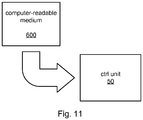
- embodiments of the present invention may be embedded in a computer program product, which enables implementation of the method and functions described herein. Therefore, according to embodiments of the present invention, there is provided a computer program product, comprising instructions arranged to cause the programmable control unit to perform the steps of any of the embodiments of said methods.
- the computer program product may comprise program code which is stored on a computer readable medium 600, as illustrated in Fig. 11 , which can be loaded and executed by said programmable control unit, to cause it to perform the steps of any of the embodiments of said methods.
- the computer-readable medium 600 may e.g. be a non-transitory computer-readable medium.
Landscapes
- Engineering & Computer Science (AREA)
- Signal Processing (AREA)
- Computer Networks & Wireless Communication (AREA)
- Power Engineering (AREA)
- Circuits Of Receivers In General (AREA)
- Input Circuits Of Receivers And Coupling Of Receivers And Audio Equipment (AREA)
- Transceivers (AREA)
- Mobile Radio Communication Systems (AREA)
- Noise Elimination (AREA)
Claims (15)
- Funkempfängerschaltung (10) für ein zellulares Kommunikationssystem, umfassend:einen ersten Direktmischempfänger (30), der dazu ausgelegt, in Wirkbeziehung mit einer Antenne (15) verbunden zu werden und umfassend einen Quadraturmischer, der dazu ausgelegt ist, von einem ersten Lokaloszillator (LO)-Signal angetrieben zu werden, eine Filtereinheit (120), die mit einem Ausgangsanschluss des Quadraturmischers verbunden ist, und eine Analog-Digital-Wandler, ADC,-Einheit (130), die mit einem Ausgangsanschluss der Filtereinheit (120) verbunden ist;einen zweiten Direktmischempfänger (40), der dazu ausgelegt ist, in Wirkbeziehung mit der gleichen Antenne (15) verbunden zu werden und umfassend einen Quadraturmischer, der dazu ausgelegt ist, von einem zweiten Lokaloszillator (LO)-Signal angetrieben zu werden, eine Filtereinheit (220), die mit einem Ausgangsanschluss des Quadraturmischers verbunden ist, und eine ADC-Einheit (230), die mit einem Ausgangsanschluss der Filtereinheit (220) verbunden ist; undeinen Digitalsignalprozessor, der zum Verarbeiten von Ausgangssignalen von der ADC-Einheit des ersten Digitalsignalprozessors und der ADC-Einheit des zweiten Digitalsignalprozessors konfiguriert ist;wobei die Funkempfängerschaltung (10) Folgendes aufweist:eine erste Betriebsart, die ein Carrier Aggregation-Modus ist, wobei die ersten und zweiten LO-Signale verschieden Frequenzen haben, wodurch der erste Direktmischempfänger (30) und der zweite Direktmischempfänger (40) einsatzbereit sind für den Empfang verschiedener Hochfrequenzträger; undeine zweite Betriebsart, die nicht ein Carrier Aggregation-Modus ist, wobei die ersten und zweiten LO-Signale die gleiche Frequenz haben, wodurch der erste Direktmischempfänger (30) und der zweite Direktmischempfänger (40) einsatzbereit sind für den Empfang des gleichen Hochfrequenzträgers.
- Funkempfängerschaltung (10) nach Anspruch 1, umfassend einen rauscharmen Verstärker (60), der dazu ausgelegt ist, sowohl den ersten Direktmischempfänger (30) als auch den zweiten Direktmischempfänger (40) in Wirkbeziehung mit der Antenne (15) zu verbinden.
- Funkempfängerschaltung (10) nach Anspruch 1 oder 2, wobei der Digitalsignalprozessor dazu konfiguriert ist, im zweiten Modus ein Ausgangssignal der ADC-Einheit des ersten Direktmischempfängers (30) mit einem Ausgangssignal der ADC-Einheit des zweiten Digitalsignalprozessors (40) zu kombinieren und dadurch ein kombiniertes Ausgangssignal zu erzeugen.
- Funkempfängerschaltung (10) nach Anspruch 1 oder 2, wobei der Digitalsignalprozessor dazu konfiguriert ist, im zweiten Modus ein Ausgangssignal der ADC-Einheit des ersten Direktmischempfängers (30) und ein Ausgangssignal der ADC-Einheit des zweiten Digitalsignalprozessors (40) getrennt zu verarbeiten und dadurch jeweils ein erstes verarbeitetes Signal und ein zweites verarbeitetes Signal zu erzeugen; wobei beim Betrieb im zweiten Modus der erste Direktmischempfänger dazu gesteuert wird, eine höhere Verstärkung zu haben, als der zweite Direktmischempfänger.
- Funkempfängerschaltung (10) nach Anspruch 4, wobei der Digitalsignalprozessor (70) dazu ausgelegt ist, Signalstärkemessungen auf dem Ausgangssignal von der ADC-Einheit des ersten Direktmischempfängers (30) und auf dem Ausgangssignal von der ADC-Einheit des zweiten Digitalsignalprozessors (40) durchzuführen.
- Funkempfängerschaltung (10) nach Anspruch 5, wobei der Digitalsignalprozessor (70) dazu ausgelegt ist, die Signalstärkemessungen durchzuführen, um eine Verstärkungseinstellung zu ermitteln, die während weiterem Empfang vom gleichen Hochfrequenzträger angewendet werden soll.
- Funkkommunikationsanordnung (1) für ein zellulares Kommunikationssystem, umfassend:eine Funkempfängerschaltung (10) nach einem der vorhergehenden Ansprüche; undeine Antenne (15), mit der sowohl der erste Direktmischempfänger als auch den zweiten Direktmischempfänger der Funkempfängerschaltung (10) in Wirkbeziehung stehen.
- Funkkommunikationsanordnung (1) nach Anspruch 7, wobei die Funkkommunikationsanordnung (1) ein Endgerät für ein zellulares Kommunikationssystem ist.
- Funkkommunikationsanordnung (1) nach Anspruch 8, wobei das Endgerät ein Mobiltelefon, ein Tabletcomputer, ein tragbarer Computer ist.
- Funkkommunikationsanordnung nach Anspruch 8, wobei das Endgerät eine Kommunikationsvorrichtung des Maschinentyps ist.
- Verfahren zum Betreiben einer Funkempfängerschaltung (10) für ein zellulares Kommunikationssystem, wobei die Funkempfängerschaltung Folgendes umfasst:einen ersten Direktmischempfänger (30), der dazu ausgelegt, in Wirkbeziehung mit einer Antenne (15) verbunden zu werden und umfassend einen Quadraturmischer, der dazu ausgelegt ist, von einem ersten Lokaloszillator (LO)-Signal angetrieben zu werden, eine Filtereinheit, die mit einem Ausgangsanschluss des Quadraturmischers verbunden ist, und eine Analog-Digital-Wandler (ADC)-Einheit, die mit einem Ausgangsanschluss der Filtereinheit verbunden ist;einen zweiten Direktmischempfänger (40), der dazu ausgelegt ist, in Wirkbeziehung mit der gleichen Antenne (15) verbunden zu werden und umfassend einen Quadraturmischer, der dazu ausgelegt ist, von einem zweiten Lokaloszillator (LO)-Signal angetrieben zu werden, eine Filtereinheit, die mit einem Ausgangsanschluss des Quadraturmischers verbunden ist, und eine ADC-Einheit, die mit einem Ausgangsanschluss der Filtereinheit verbunden ist; undeinen Digitalsignalprozessor, der zum Verarbeiten von Ausgangssignalen von der ADC-Einheit des ersten Digitalsignalprozessors und der ADC-Einheit des zweiten Digitalsignalprozessors konfiguriert ist;wobei das Verfahren Folgendes umfasst:Steuern, in einer ersten Betriebsart, die ein Carrier Aggregation-Modus ist, dass die ersten und zweiten LO-Signale verschieden Frequenzen haben, wodurch der erste Direktmischempfänger und der zweite Direktmischempfänger einsatzbereit sind für den Empfang verschiedener Hochfrequenzträger; undSteuern, in einer zweiten Betriebsart, die nicht ein Carrier Aggregation-Modus ist, dass die ersten und zweiten LO-Signale die gleiche Frequenz haben, wodurch der erste Direktmischempfänger und der zweite Direktmischempfänger einsatzbereit sind für den Empfang des gleichen Hochfrequenzträgers.
- Verfahren nach Anspruch 11, umfassend, im zweiten Modus, das Kombinieren durch den Digitalsignalprozessor, eines Ausgangssignals der ADC-Einheit des ersten Direktmischempfängers (30) mit einem Ausgangssignal der ADC-Einheit des zweiten Digitalsignalprozessors (40) und dadurch Erzeugen eines kombinierten Ausgangssignals.
- Verfahren nach Anspruch 11, umfassend, im zweiten Modus, das Steuern des ersten Direktmischempfängers eine höhere Verstärkung zu haben, als der zweite Direktmischempfänger; und
das getrennte Verarbeiten, durch den Digitalsignalprozessor eines Ausgangssignals der ADC-Einheit des ersten Direktmischempfängers (30) und eines Ausgangssignals der ADC-Einheit des zweiten Digitalsignalprozessors (40) und dadurch Erzeugen jeweils eines ersten verarbeiteten Signals und eines zweiten verarbeiteten Signals. - Verfahren nach Anspruch 13, umfassend
Durchführen, durch den Digitalsignalprozessor (70), von Signalstärkemessungen auf dem Ausgangssignal von der ADC-Einheit des ersten Direktmischempfängers (30) und auf dem Ausgangssignal von der ADC-Einheit des zweiten Digitalsignalprozessors (40). - Verfahren nach Anspruch 14, umfassend Ermitteln, durch den Digitalsignalprozessor (70), einer Verstärkungseinstellung, die während weiterem Empfang vom gleichen Hochfrequenzträger angewendet werden soll, auf Grundlage der Signalstärkemessungen.
Priority Applications (4)
| Application Number | Priority Date | Filing Date | Title |
|---|---|---|---|
| PL18154125T PL3355478T3 (pl) | 2014-09-10 | 2014-09-10 | Odbiornik radiowy do agregacji nośnych |
| DK18154125T DK3355478T3 (da) | 2014-09-10 | 2014-09-10 | Radiomodtager til bæreraggregering |
| ES18154125T ES2754790T3 (es) | 2014-09-10 | 2014-09-10 | Receptor de radio para agregación de portadora |
| EP18154125.1A EP3355478B1 (de) | 2014-09-10 | 2014-09-10 | Funkempfänger für trägeraggregation |
Applications Claiming Priority (3)
| Application Number | Priority Date | Filing Date | Title |
|---|---|---|---|
| EP14761994.4A EP3192179B1 (de) | 2014-09-10 | 2014-09-10 | Funkempfänger für trägeraggregation |
| EP18154125.1A EP3355478B1 (de) | 2014-09-10 | 2014-09-10 | Funkempfänger für trägeraggregation |
| PCT/EP2014/069280 WO2016037649A1 (en) | 2014-09-10 | 2014-09-10 | Radio receiver for carrier aggregation |
Related Parent Applications (2)
| Application Number | Title | Priority Date | Filing Date |
|---|---|---|---|
| EP14761994.4A Division EP3192179B1 (de) | 2014-09-10 | 2014-09-10 | Funkempfänger für trägeraggregation |
| EP14761994.4A Division-Into EP3192179B1 (de) | 2014-09-10 | 2014-09-10 | Funkempfänger für trägeraggregation |
Publications (2)
| Publication Number | Publication Date |
|---|---|
| EP3355478A1 EP3355478A1 (de) | 2018-08-01 |
| EP3355478B1 true EP3355478B1 (de) | 2019-08-07 |
Family
ID=51535429
Family Applications (2)
| Application Number | Title | Priority Date | Filing Date |
|---|---|---|---|
| EP18154125.1A Active EP3355478B1 (de) | 2014-09-10 | 2014-09-10 | Funkempfänger für trägeraggregation |
| EP14761994.4A Active EP3192179B1 (de) | 2014-09-10 | 2014-09-10 | Funkempfänger für trägeraggregation |
Family Applications After (1)
| Application Number | Title | Priority Date | Filing Date |
|---|---|---|---|
| EP14761994.4A Active EP3192179B1 (de) | 2014-09-10 | 2014-09-10 | Funkempfänger für trägeraggregation |
Country Status (17)
| Country | Link |
|---|---|
| US (3) | US9344318B2 (de) |
| EP (2) | EP3355478B1 (de) |
| JP (1) | JP6307662B2 (de) |
| KR (2) | KR101866707B1 (de) |
| CN (1) | CN106688187B (de) |
| AU (2) | AU2014405866B2 (de) |
| BR (1) | BR112017003677A2 (de) |
| CA (1) | CA2960736C (de) |
| DK (2) | DK3355478T3 (de) |
| ES (2) | ES2671558T3 (de) |
| HU (1) | HUE037929T2 (de) |
| IL (1) | IL250669A (de) |
| MX (1) | MX366605B (de) |
| MY (1) | MY191230A (de) |
| PL (2) | PL3355478T3 (de) |
| RU (1) | RU2657244C1 (de) |
| WO (1) | WO2016037649A1 (de) |
Families Citing this family (15)
| Publication number | Priority date | Publication date | Assignee | Title |
|---|---|---|---|---|
| EP3355478B1 (de) * | 2014-09-10 | 2019-08-07 | Telefonaktiebolaget LM Ericsson (publ) | Funkempfänger für trägeraggregation |
| US9755767B2 (en) * | 2014-10-31 | 2017-09-05 | Qualcomm Incorporated | Mechanism to measure, report, and allocate a highest possible rank for each cell in a carrier aggregation (CA) mode receiver-limited user equipment (UE) |
| US10263754B2 (en) * | 2015-09-21 | 2019-04-16 | Qualcomm Incorporated | Wireless device architecture to support very-high-reliability (VHR) communication |
| US10574278B2 (en) | 2015-11-13 | 2020-02-25 | Texas Instruments Incorporated | High dynamic range ask wake-up receiver |
| US10389456B2 (en) | 2016-08-26 | 2019-08-20 | Texas Instruments Incorporated | Wake up receiver using multiphase peak detector and demodulator |
| WO2018098825A1 (zh) * | 2016-12-02 | 2018-06-07 | 华为技术有限公司 | 一种工作模式的切换方法及用户设备 |
| KR102631348B1 (ko) | 2018-04-19 | 2024-01-31 | 삼성전자주식회사 | 반송파 집적(Carrier Aggregation)을 이용하여 신호를 송수신하는 무선 통신 장치 |
| WO2020005224A1 (en) * | 2018-06-27 | 2020-01-02 | Intel IP Corporation | Dynamic low if mechanism for blocker avoidance |
| KR102653889B1 (ko) * | 2019-10-18 | 2024-04-02 | 삼성전자주식회사 | 반송파 집성을 지원하는 수신기 및 이를 포함하는 무선 통신 장치 |
| KR102653890B1 (ko) * | 2019-10-18 | 2024-04-02 | 삼성전자주식회사 | 반송파 집성을 지원하는 rfic 및 이를 포함하는 무선 통신 장치 |
| CN113691269B (zh) * | 2021-08-30 | 2022-03-25 | 上海航天测控通信研究所 | 一种可变频点的星用高灵敏度测控接收机 |
| EP4164134B1 (de) * | 2021-10-06 | 2025-07-02 | Nxp B.V. | Kommunikationsvorrichtung und betriebsverfahren |
| CN113872622B (zh) * | 2021-10-15 | 2022-05-27 | 上海航天测控通信研究所 | 一种可变频点的星用测控发射机 |
| EP4354742A1 (de) * | 2022-10-12 | 2024-04-17 | Nokia Technologies Oy | Flexibler empfang |
| GB2642286A (en) * | 2024-06-28 | 2026-01-07 | Nokia Technologies Oy | Method, apparatus and computer program |
Family Cites Families (18)
| Publication number | Priority date | Publication date | Assignee | Title |
|---|---|---|---|---|
| US8363744B2 (en) | 2001-06-10 | 2013-01-29 | Aloft Media, Llc | Method and system for robust, secure, and high-efficiency voice and packet transmission over ad-hoc, mesh, and MIMO communication networks |
| EP1944887B1 (de) | 2007-01-11 | 2013-11-06 | Harman Becker Automotive Systems GmbH | Radioempfänger für hybride Sendersysteme |
| EP2120336B1 (de) * | 2008-05-14 | 2010-07-14 | Telefonaktiebolaget L M Ericsson (Publ) | Verfahren zur Steuerung einer Empfängerverstärkung |
| KR101347295B1 (ko) * | 2010-11-02 | 2014-01-03 | 한국전자통신연구원 | 반송파 집적 환경에서 스케일러블 대역폭을 지원하는 수신장치 및 송신장치 |
| US9602145B2 (en) * | 2011-02-07 | 2017-03-21 | Qualcomm Incorporated | Insertion loss improvement in a multi-band device |
| US9252827B2 (en) | 2011-06-27 | 2016-02-02 | Qualcomm Incorporated | Signal splitting carrier aggregation receiver architecture |
| US8892057B2 (en) * | 2011-08-23 | 2014-11-18 | Rf Micro Devices, Inc. | Carrier aggregation radio system |
| EP2590351A3 (de) * | 2011-11-04 | 2013-05-22 | ST-Ericsson SA | Aggregation nicht aneinandergrenzender Träger |
| WO2013138755A1 (en) * | 2012-03-15 | 2013-09-19 | Broadcom Corporation | Reducing complexity and power consumption in cellular networks with carrier aggregation |
| GB2500265B (en) * | 2012-03-16 | 2014-03-05 | Broadcom Corp | Reconfigurable radio frequency circuits and methods of receiving |
| CN103517401A (zh) * | 2012-06-29 | 2014-01-15 | 中兴通讯股份有限公司 | 无线传输方法、装置及系统 |
| WO2014007697A1 (en) * | 2012-07-04 | 2014-01-09 | Telefonaktiebolaget L M Ericsson (Publ) | A radio network node, a user equipment and methods therein |
| TWI465050B (zh) * | 2012-12-19 | 2014-12-11 | Ind Tech Res Inst | 載波聚合接收裝置與發射裝置及收發裝置 |
| KR102180573B1 (ko) * | 2013-10-22 | 2020-11-18 | 삼성전자주식회사 | 신호를 수신하는 방법 및 전자 장치 |
| US9628163B2 (en) * | 2014-03-25 | 2017-04-18 | Marvell International Ltd. | Low-complexity communication terminal with enhanced receive diversity |
| US9681447B2 (en) * | 2014-05-15 | 2017-06-13 | Qualcomm Incorporated | Dynamic local oscillator (LO) scheme and switchable receive (RX) chain for carrier aggregation |
| US9712226B2 (en) * | 2014-05-15 | 2017-07-18 | Qualcomm Incorporated | Multi-way diversity receiver with multiple synthesizers in a carrier aggregation transceiver |
| EP3355478B1 (de) * | 2014-09-10 | 2019-08-07 | Telefonaktiebolaget LM Ericsson (publ) | Funkempfänger für trägeraggregation |
-
2014
- 2014-09-10 EP EP18154125.1A patent/EP3355478B1/de active Active
- 2014-09-10 MX MX2017003081A patent/MX366605B/es active IP Right Grant
- 2014-09-10 PL PL18154125T patent/PL3355478T3/pl unknown
- 2014-09-10 CN CN201480081831.4A patent/CN106688187B/zh not_active Expired - Fee Related
- 2014-09-10 MY MYPI2017700690A patent/MY191230A/en unknown
- 2014-09-10 PL PL14761994T patent/PL3192179T3/pl unknown
- 2014-09-10 DK DK18154125T patent/DK3355478T3/da active
- 2014-09-10 DK DK14761994.4T patent/DK3192179T3/en active
- 2014-09-10 CA CA2960736A patent/CA2960736C/en not_active Expired - Fee Related
- 2014-09-10 US US14/768,380 patent/US9344318B2/en not_active Expired - Fee Related
- 2014-09-10 RU RU2017111650A patent/RU2657244C1/ru active
- 2014-09-10 KR KR1020177009670A patent/KR101866707B1/ko not_active Expired - Fee Related
- 2014-09-10 KR KR1020187015374A patent/KR102063564B1/ko not_active Expired - Fee Related
- 2014-09-10 WO PCT/EP2014/069280 patent/WO2016037649A1/en not_active Ceased
- 2014-09-10 AU AU2014405866A patent/AU2014405866B2/en not_active Ceased
- 2014-09-10 EP EP14761994.4A patent/EP3192179B1/de active Active
- 2014-09-10 JP JP2017513536A patent/JP6307662B2/ja not_active Expired - Fee Related
- 2014-09-10 BR BR112017003677A patent/BR112017003677A2/pt active Search and Examination
- 2014-09-10 ES ES14761994.4T patent/ES2671558T3/es active Active
- 2014-09-10 ES ES18154125T patent/ES2754790T3/es active Active
- 2014-09-10 HU HUE14761994A patent/HUE037929T2/hu unknown
-
2016
- 2016-04-25 US US15/137,669 patent/US10014824B2/en active Active
-
2017
- 2017-02-19 IL IL250669A patent/IL250669A/en active IP Right Grant
-
2018
- 2018-02-26 AU AU2018201359A patent/AU2018201359B2/en not_active Ceased
- 2018-06-01 US US15/995,811 patent/US10326403B2/en not_active Expired - Fee Related
Non-Patent Citations (1)
| Title |
|---|
| None * |
Also Published As
Similar Documents
| Publication | Publication Date | Title |
|---|---|---|
| US10326403B2 (en) | Radio receiver for carrier aggregation | |
| US9674810B2 (en) | Method, apparatus and computer program for search and synchronisation | |
| US10727800B2 (en) | Method for gain control and related wireless receivers and devices | |
| US20170104507A1 (en) | Adjusting local oscillator frequency during gaps in data transmission | |
| US20160014724A1 (en) | Wireless communication device and wireless communication method | |
| WO2016200358A1 (en) | Enhanced overlaid code division multiple access (cdma) | |
| OA20931A (en) | Radio receiver carrier aggregation | |
| RU2710538C2 (ru) | Радиоприемник для агрегации несущих | |
| US20130064145A1 (en) | Method, apparatus and computer program for setting a radio frequency gain | |
| US20250392328A1 (en) | Fast automatic gain control in a wireless receiver | |
| GB2630809A (en) | Irregular channel bandwidth support mechanism | |
| US9191905B2 (en) | Method, apparatus and computer readable medium for setting a radio frequency gain | |
| WO2012176139A1 (en) | Method, apparatus and computer program for setting a radio frequency gain |
Legal Events
| Date | Code | Title | Description |
|---|---|---|---|
| PUAI | Public reference made under article 153(3) epc to a published international application that has entered the european phase |
Free format text: ORIGINAL CODE: 0009012 |
|
| STAA | Information on the status of an ep patent application or granted ep patent |
Free format text: STATUS: THE APPLICATION HAS BEEN PUBLISHED |
|
| AC | Divisional application: reference to earlier application |
Ref document number: 3192179 Country of ref document: EP Kind code of ref document: P |
|
| AK | Designated contracting states |
Kind code of ref document: A1 Designated state(s): AL AT BE BG CH CY CZ DE DK EE ES FI FR GB GR HR HU IE IS IT LI LT LU LV MC MK MT NL NO PL PT RO RS SE SI SK SM TR |
|
| STAA | Information on the status of an ep patent application or granted ep patent |
Free format text: STATUS: REQUEST FOR EXAMINATION WAS MADE |
|
| GRAP | Despatch of communication of intention to grant a patent |
Free format text: ORIGINAL CODE: EPIDOSNIGR1 |
|
| STAA | Information on the status of an ep patent application or granted ep patent |
Free format text: STATUS: GRANT OF PATENT IS INTENDED |
|
| 17P | Request for examination filed |
Effective date: 20190123 |
|
| RBV | Designated contracting states (corrected) |
Designated state(s): AL AT BE BG CH CY CZ DE DK EE ES FI FR GB GR HR HU IE IS IT LI LT LU LV MC MK MT NL NO PL PT RO RS SE SI SK SM TR |
|
| INTG | Intention to grant announced |
Effective date: 20190306 |
|
| RIN1 | Information on inventor provided before grant (corrected) |
Inventor name: JAKOBSSON, PETER Inventor name: NILSSON, MAGNUS |
|
| GRAS | Grant fee paid |
Free format text: ORIGINAL CODE: EPIDOSNIGR3 |
|
| GRAA | (expected) grant |
Free format text: ORIGINAL CODE: 0009210 |
|
| STAA | Information on the status of an ep patent application or granted ep patent |
Free format text: STATUS: THE PATENT HAS BEEN GRANTED |
|
| AC | Divisional application: reference to earlier application |
Ref document number: 3192179 Country of ref document: EP Kind code of ref document: P |
|
| AK | Designated contracting states |
Kind code of ref document: B1 Designated state(s): AL AT BE BG CH CY CZ DE DK EE ES FI FR GB GR HR HU IE IS IT LI LT LU LV MC MK MT NL NO PL PT RO RS SE SI SK SM TR |
|
| REG | Reference to a national code |
Ref country code: GB Ref legal event code: FG4D |
|
| REG | Reference to a national code |
Ref country code: CH Ref legal event code: EP Ref country code: AT Ref legal event code: REF Ref document number: 1165392 Country of ref document: AT Kind code of ref document: T Effective date: 20190815 |
|
| REG | Reference to a national code |
Ref country code: DE Ref legal event code: R096 Ref document number: 602014051618 Country of ref document: DE |
|
| REG | Reference to a national code |
Ref country code: IE Ref legal event code: FG4D |
|
| REG | Reference to a national code |
Ref country code: NL Ref legal event code: FP |
|
| REG | Reference to a national code |
Ref country code: DK Ref legal event code: T3 Effective date: 20191029 |
|
| REG | Reference to a national code |
Ref country code: NO Ref legal event code: T2 Effective date: 20190807 |
|
| REG | Reference to a national code |
Ref country code: LT Ref legal event code: MG4D |
|
| PG25 | Lapsed in a contracting state [announced via postgrant information from national office to epo] |
Ref country code: HR Free format text: LAPSE BECAUSE OF FAILURE TO SUBMIT A TRANSLATION OF THE DESCRIPTION OR TO PAY THE FEE WITHIN THE PRESCRIBED TIME-LIMIT Effective date: 20190807 Ref country code: LT Free format text: LAPSE BECAUSE OF FAILURE TO SUBMIT A TRANSLATION OF THE DESCRIPTION OR TO PAY THE FEE WITHIN THE PRESCRIBED TIME-LIMIT Effective date: 20190807 Ref country code: BG Free format text: LAPSE BECAUSE OF FAILURE TO SUBMIT A TRANSLATION OF THE DESCRIPTION OR TO PAY THE FEE WITHIN THE PRESCRIBED TIME-LIMIT Effective date: 20191107 Ref country code: FI Free format text: LAPSE BECAUSE OF FAILURE TO SUBMIT A TRANSLATION OF THE DESCRIPTION OR TO PAY THE FEE WITHIN THE PRESCRIBED TIME-LIMIT Effective date: 20190807 Ref country code: PT Free format text: LAPSE BECAUSE OF FAILURE TO SUBMIT A TRANSLATION OF THE DESCRIPTION OR TO PAY THE FEE WITHIN THE PRESCRIBED TIME-LIMIT Effective date: 20191209 Ref country code: SE Free format text: LAPSE BECAUSE OF FAILURE TO SUBMIT A TRANSLATION OF THE DESCRIPTION OR TO PAY THE FEE WITHIN THE PRESCRIBED TIME-LIMIT Effective date: 20190807 |
|
| REG | Reference to a national code |
Ref country code: AT Ref legal event code: MK05 Ref document number: 1165392 Country of ref document: AT Kind code of ref document: T Effective date: 20190807 |
|
| PG25 | Lapsed in a contracting state [announced via postgrant information from national office to epo] |
Ref country code: RS Free format text: LAPSE BECAUSE OF FAILURE TO SUBMIT A TRANSLATION OF THE DESCRIPTION OR TO PAY THE FEE WITHIN THE PRESCRIBED TIME-LIMIT Effective date: 20190807 Ref country code: IS Free format text: LAPSE BECAUSE OF FAILURE TO SUBMIT A TRANSLATION OF THE DESCRIPTION OR TO PAY THE FEE WITHIN THE PRESCRIBED TIME-LIMIT Effective date: 20191207 Ref country code: LV Free format text: LAPSE BECAUSE OF FAILURE TO SUBMIT A TRANSLATION OF THE DESCRIPTION OR TO PAY THE FEE WITHIN THE PRESCRIBED TIME-LIMIT Effective date: 20190807 Ref country code: AL Free format text: LAPSE BECAUSE OF FAILURE TO SUBMIT A TRANSLATION OF THE DESCRIPTION OR TO PAY THE FEE WITHIN THE PRESCRIBED TIME-LIMIT Effective date: 20190807 Ref country code: GR Free format text: LAPSE BECAUSE OF FAILURE TO SUBMIT A TRANSLATION OF THE DESCRIPTION OR TO PAY THE FEE WITHIN THE PRESCRIBED TIME-LIMIT Effective date: 20191108 |
|
| REG | Reference to a national code |
Ref country code: ES Ref legal event code: FG2A Ref document number: 2754790 Country of ref document: ES Kind code of ref document: T3 Effective date: 20200420 |
|
| PG25 | Lapsed in a contracting state [announced via postgrant information from national office to epo] |
Ref country code: EE Free format text: LAPSE BECAUSE OF FAILURE TO SUBMIT A TRANSLATION OF THE DESCRIPTION OR TO PAY THE FEE WITHIN THE PRESCRIBED TIME-LIMIT Effective date: 20190807 Ref country code: AT Free format text: LAPSE BECAUSE OF FAILURE TO SUBMIT A TRANSLATION OF THE DESCRIPTION OR TO PAY THE FEE WITHIN THE PRESCRIBED TIME-LIMIT Effective date: 20190807 Ref country code: RO Free format text: LAPSE BECAUSE OF FAILURE TO SUBMIT A TRANSLATION OF THE DESCRIPTION OR TO PAY THE FEE WITHIN THE PRESCRIBED TIME-LIMIT Effective date: 20190807 |
|
| PG25 | Lapsed in a contracting state [announced via postgrant information from national office to epo] |
Ref country code: IS Free format text: LAPSE BECAUSE OF FAILURE TO SUBMIT A TRANSLATION OF THE DESCRIPTION OR TO PAY THE FEE WITHIN THE PRESCRIBED TIME-LIMIT Effective date: 20200224 Ref country code: MC Free format text: LAPSE BECAUSE OF FAILURE TO SUBMIT A TRANSLATION OF THE DESCRIPTION OR TO PAY THE FEE WITHIN THE PRESCRIBED TIME-LIMIT Effective date: 20190807 Ref country code: SK Free format text: LAPSE BECAUSE OF FAILURE TO SUBMIT A TRANSLATION OF THE DESCRIPTION OR TO PAY THE FEE WITHIN THE PRESCRIBED TIME-LIMIT Effective date: 20190807 Ref country code: SM Free format text: LAPSE BECAUSE OF FAILURE TO SUBMIT A TRANSLATION OF THE DESCRIPTION OR TO PAY THE FEE WITHIN THE PRESCRIBED TIME-LIMIT Effective date: 20190807 |
|
| REG | Reference to a national code |
Ref country code: DE Ref legal event code: R097 Ref document number: 602014051618 Country of ref document: DE |
|
| PLBE | No opposition filed within time limit |
Free format text: ORIGINAL CODE: 0009261 |
|
| STAA | Information on the status of an ep patent application or granted ep patent |
Free format text: STATUS: NO OPPOSITION FILED WITHIN TIME LIMIT |
|
| PG2D | Information on lapse in contracting state deleted |
Ref country code: IS |
|
| PG25 | Lapsed in a contracting state [announced via postgrant information from national office to epo] |
Ref country code: IE Free format text: LAPSE BECAUSE OF NON-PAYMENT OF DUE FEES Effective date: 20190910 Ref country code: LU Free format text: LAPSE BECAUSE OF NON-PAYMENT OF DUE FEES Effective date: 20190910 |
|
| REG | Reference to a national code |
Ref country code: BE Ref legal event code: MM Effective date: 20190930 |
|
| 26N | No opposition filed |
Effective date: 20200603 |
|
| PG25 | Lapsed in a contracting state [announced via postgrant information from national office to epo] |
Ref country code: SI Free format text: LAPSE BECAUSE OF FAILURE TO SUBMIT A TRANSLATION OF THE DESCRIPTION OR TO PAY THE FEE WITHIN THE PRESCRIBED TIME-LIMIT Effective date: 20190807 Ref country code: BE Free format text: LAPSE BECAUSE OF NON-PAYMENT OF DUE FEES Effective date: 20190930 |
|
| PG25 | Lapsed in a contracting state [announced via postgrant information from national office to epo] |
Ref country code: CY Free format text: LAPSE BECAUSE OF FAILURE TO SUBMIT A TRANSLATION OF THE DESCRIPTION OR TO PAY THE FEE WITHIN THE PRESCRIBED TIME-LIMIT Effective date: 20190807 |
|
| PG25 | Lapsed in a contracting state [announced via postgrant information from national office to epo] |
Ref country code: HU Free format text: LAPSE BECAUSE OF FAILURE TO SUBMIT A TRANSLATION OF THE DESCRIPTION OR TO PAY THE FEE WITHIN THE PRESCRIBED TIME-LIMIT; INVALID AB INITIO Effective date: 20140910 Ref country code: MT Free format text: LAPSE BECAUSE OF FAILURE TO SUBMIT A TRANSLATION OF THE DESCRIPTION OR TO PAY THE FEE WITHIN THE PRESCRIBED TIME-LIMIT Effective date: 20190807 |
|
| PGFP | Annual fee paid to national office [announced via postgrant information from national office to epo] |
Ref country code: CZ Payment date: 20210831 Year of fee payment: 8 Ref country code: IT Payment date: 20210922 Year of fee payment: 8 Ref country code: NL Payment date: 20210926 Year of fee payment: 8 Ref country code: FR Payment date: 20210927 Year of fee payment: 8 |
|
| PGFP | Annual fee paid to national office [announced via postgrant information from national office to epo] |
Ref country code: NO Payment date: 20210929 Year of fee payment: 8 Ref country code: PL Payment date: 20210820 Year of fee payment: 8 Ref country code: GB Payment date: 20210927 Year of fee payment: 8 Ref country code: TR Payment date: 20210827 Year of fee payment: 8 Ref country code: DK Payment date: 20210929 Year of fee payment: 8 |
|
| PGFP | Annual fee paid to national office [announced via postgrant information from national office to epo] |
Ref country code: ES Payment date: 20211001 Year of fee payment: 8 |
|
| PGFP | Annual fee paid to national office [announced via postgrant information from national office to epo] |
Ref country code: CH Payment date: 20211004 Year of fee payment: 8 |
|
| PG25 | Lapsed in a contracting state [announced via postgrant information from national office to epo] |
Ref country code: MK Free format text: LAPSE BECAUSE OF FAILURE TO SUBMIT A TRANSLATION OF THE DESCRIPTION OR TO PAY THE FEE WITHIN THE PRESCRIBED TIME-LIMIT Effective date: 20190807 |
|
| PGFP | Annual fee paid to national office [announced via postgrant information from national office to epo] |
Ref country code: DE Payment date: 20220629 Year of fee payment: 9 |
|
| REG | Reference to a national code |
Ref country code: NO Ref legal event code: MMEP |
|
| PG25 | Lapsed in a contracting state [announced via postgrant information from national office to epo] |
Ref country code: CZ Free format text: LAPSE BECAUSE OF NON-PAYMENT OF DUE FEES Effective date: 20220910 |
|
| REG | Reference to a national code |
Ref country code: CH Ref legal event code: PL |
|
| REG | Reference to a national code |
Ref country code: DK Ref legal event code: EBP Effective date: 20220930 |
|
| REG | Reference to a national code |
Ref country code: NL Ref legal event code: MM Effective date: 20221001 |
|
| GBPC | Gb: european patent ceased through non-payment of renewal fee |
Effective date: 20220910 |
|
| PG25 | Lapsed in a contracting state [announced via postgrant information from national office to epo] |
Ref country code: NL Free format text: LAPSE BECAUSE OF NON-PAYMENT OF DUE FEES Effective date: 20221001 |
|
| PG25 | Lapsed in a contracting state [announced via postgrant information from national office to epo] |
Ref country code: NO Free format text: LAPSE BECAUSE OF NON-PAYMENT OF DUE FEES Effective date: 20220930 Ref country code: LI Free format text: LAPSE BECAUSE OF NON-PAYMENT OF DUE FEES Effective date: 20220930 Ref country code: FR Free format text: LAPSE BECAUSE OF NON-PAYMENT OF DUE FEES Effective date: 20220930 Ref country code: CH Free format text: LAPSE BECAUSE OF NON-PAYMENT OF DUE FEES Effective date: 20220930 |
|
| REG | Reference to a national code |
Ref country code: ES Ref legal event code: FD2A Effective date: 20231027 |
|
| PG25 | Lapsed in a contracting state [announced via postgrant information from national office to epo] |
Ref country code: IT Free format text: LAPSE BECAUSE OF NON-PAYMENT OF DUE FEES Effective date: 20220910 Ref country code: GB Free format text: LAPSE BECAUSE OF NON-PAYMENT OF DUE FEES Effective date: 20220910 Ref country code: DK Free format text: LAPSE BECAUSE OF NON-PAYMENT OF DUE FEES Effective date: 20220930 |
|
| PG25 | Lapsed in a contracting state [announced via postgrant information from national office to epo] |
Ref country code: ES Free format text: LAPSE BECAUSE OF NON-PAYMENT OF DUE FEES Effective date: 20220911 |
|
| PG25 | Lapsed in a contracting state [announced via postgrant information from national office to epo] |
Ref country code: ES Free format text: LAPSE BECAUSE OF NON-PAYMENT OF DUE FEES Effective date: 20220911 |
|
| REG | Reference to a national code |
Ref country code: DE Ref legal event code: R119 Ref document number: 602014051618 Country of ref document: DE |
|
| PG25 | Lapsed in a contracting state [announced via postgrant information from national office to epo] |
Ref country code: PL Free format text: LAPSE BECAUSE OF NON-PAYMENT OF DUE FEES Effective date: 20220910 |
|
| PG25 | Lapsed in a contracting state [announced via postgrant information from national office to epo] |
Ref country code: DE Free format text: LAPSE BECAUSE OF NON-PAYMENT OF DUE FEES Effective date: 20240403 |