EP4154517B1 - Multidynamischer bilddetektor - Google Patents
Multidynamischer bilddetektor Download PDFInfo
- Publication number
- EP4154517B1 EP4154517B1 EP21733536.3A EP21733536A EP4154517B1 EP 4154517 B1 EP4154517 B1 EP 4154517B1 EP 21733536 A EP21733536 A EP 21733536A EP 4154517 B1 EP4154517 B1 EP 4154517B1
- Authority
- EP
- European Patent Office
- Prior art keywords
- reset
- reset curve
- light
- signal
- curve
- Prior art date
- Legal status (The legal status is an assumption and is not a legal conclusion. Google has not performed a legal analysis and makes no representation as to the accuracy of the status listed.)
- Active
Links
Images


Classifications
-
- H—ELECTRICITY
- H04—ELECTRIC COMMUNICATION TECHNIQUE
- H04N—PICTORIAL COMMUNICATION, e.g. TELEVISION
- H04N25/00—Circuitry of solid-state image sensors [SSIS]; Control thereof
- H04N25/50—Control of the SSIS exposure
- H04N25/57—Control of the dynamic range
- H04N25/571—Control of the dynamic range involving a non-linear response
- H04N25/575—Control of the dynamic range involving a non-linear response with a response composed of multiple slopes
-
- H—ELECTRICITY
- H04—ELECTRIC COMMUNICATION TECHNIQUE
- H04N—PICTORIAL COMMUNICATION, e.g. TELEVISION
- H04N25/00—Circuitry of solid-state image sensors [SSIS]; Control thereof
- H04N25/70—SSIS architectures; Circuits associated therewith
- H04N25/76—Addressed sensors, e.g. MOS or CMOS sensors
- H04N25/779—Circuitry for scanning or addressing the pixel array
-
- H—ELECTRICITY
- H04—ELECTRIC COMMUNICATION TECHNIQUE
- H04N—PICTORIAL COMMUNICATION, e.g. TELEVISION
- H04N25/00—Circuitry of solid-state image sensors [SSIS]; Control thereof
- H04N25/70—SSIS architectures; Circuits associated therewith
- H04N25/709—Circuitry for control of the power supply
-
- H—ELECTRICITY
- H04—ELECTRIC COMMUNICATION TECHNIQUE
- H04N—PICTORIAL COMMUNICATION, e.g. TELEVISION
- H04N25/00—Circuitry of solid-state image sensors [SSIS]; Control thereof
- H04N25/70—SSIS architectures; Circuits associated therewith
- H04N25/76—Addressed sensors, e.g. MOS or CMOS sensors
- H04N25/77—Pixel circuitry, e.g. memories, A/D converters, pixel amplifiers, shared circuits or shared components
-
- H—ELECTRICITY
- H04—ELECTRIC COMMUNICATION TECHNIQUE
- H04N—PICTORIAL COMMUNICATION, e.g. TELEVISION
- H04N25/00—Circuitry of solid-state image sensors [SSIS]; Control thereof
- H04N25/70—SSIS architectures; Circuits associated therewith
- H04N25/76—Addressed sensors, e.g. MOS or CMOS sensors
- H04N25/7795—Circuitry for generating timing or clock signals
Definitions
- the present invention relates to a digital image acquisition device of the type comprising at least a plurality of photosensitive elements, or pixels, each provided with at least one reset, selection and reading terminal to respectively allow the reset and control of the discharge of the photosensor, the selection of the pixel to enable reading and the reading thereof, and control and selection elements which allow selecting the photosensitive elements individually or in subgroups and controlling the discharge thereof, in which said control elements are connected to the photosensitive elements.
- the image acquisition device ensures a high quality of images in the presence of scenes with low brightness, high brightness, and with a light intensity variable in a wide range passing from very low to very high light intensity.
- Electro-optical sensors comprising a plurality of photodetector devices adapted to detect light signals by means of a photosensitive element and to transmit them, in the form of electrical signals, to a computing unit which processes them, obtaining images. Such images are then transmitted to storage or display devices which allow a user to view such images or information derived therefrom, even over time.
- electro-optical sensors are generally based on CMOS-type (Complementary Metal Oxide Semiconductor) silicon technology, and are adapted to detect scenes with a fixed and normally limited brightness range, by means of a linear transformation of the information conveyed by the incident light into an electrical signal (linear response sensors).
- the light information is acquired during a time interval, called integration or exposure time.
- the photosensitive element discharges more or less quickly depending on the amount of incident light until the time interval defined for the integration ends, a condition in which an electrical signal is output from the photosensitive element which corresponds to the incident light, or to the state corresponding to the complete discharge of the photosensitive element, a condition defined saturation, and which means that the photosensitive element is no longer able to map the light information.
- a condition in which an electrical signal is output from the photosensitive element which corresponds to the incident light or to the state corresponding to the complete discharge of the photosensitive element, a condition defined saturation, and which means that the photosensitive element is no longer able to map the light information.
- Such sensors are normally able to offer high image quality even under highly diversified lighting conditions within the same scene, exploiting different conversion techniques and mapping the light information in a more than linear manner into a corresponding electrical signal.
- Such techniques which aim to extend the range of light intensity manageable by the photosensitive element before it reaches the saturation level, are defined as high light dynamics.
- US 2017/251151 A1 also discloses a reset pulse technique similar to the previous one.
- the architecture of the system disclosed includes the presence of a block which generates signals for PRST, RST and TX to apply reset pulses.
- the technique of acquiring multiple linear images to obtain information in different brightness ranges is also known and widespread, which are then combined to obtain a single image which contains the information deriving from the different images and thus obtaining images with high light dynamics.
- Such a technique is implemented both through the aid of software tools and directly on physical substrates, typically silicon, which integrate, in addition to the photosensitive element, also the electronics necessary to implement the control system and generate the images deriving from the combination of the acquired images.
- the advantages of this technique are the high flexibility in programming the output light dynamics, both in amplitude and shape, based on the reset control signal and, consequently, the possibility of optimizing the response in terms of dynamics and resolution in the desired light range, rather than increasing the compression thereof and obtaining very high dynamic images. All the above with the acquisition of a single image, and thus avoiding artefacts, limiting processing complexity and obtaining high quality in any light condition.
- HDRView a publicly available application
- US 7492375 a similar technique is also presented in US 7492375 .
- all the techniques known in the state of the art have the disadvantage of requiring operator intervention and being implemented entirely in software with the consequent need for a large computational load and a large memory to maintain all the information necessary to enable such a function.
- HDR monitors Another technique for solving the problem of displaying high dynamic images is the use of high dynamic light monitors, called HDR monitors, which allow a much wider number of grey levels (10-12-bit) than traditional monitors to be displayed.
- neuromorphic vision sensors are known in the state of the art which boast of operating like the human eye because they do not detect the image itself but the events occurring in the scene. These sensors are based on high dynamic image acquisition with logarithmic technique and have the advantage of producing a much smaller volume of data when dealing with complete and detailed images, but have the inherent disadvantage of containing less information, demonstrating less versatility with respect to different application fields.
- An object of the present invention is to provide an electro-optical device which can be integrated into a support element, or substrate, suitable to realize small electronic circuits, for example of silicon, and which is suitable for providing good quality images at a high repetition frequency both in the case of low brightness and in the presence of a wide range of brightnesses present in the observed scene.
- a specific object is to realize an electro-optical device which is capable of operating both in controlled and non-controlled light conditions, allowing to adapt the response dynamics of the sensor both to lighting conditions and to the needs of the user and/or the application.
- a further object of the present invention is to realize an electro-optical sensor which comprises a plurality of photosensitive elements arranged according to a matrix, or in another desired arrangement, and which allows to independently manage the reset state even of a single photosensitive element, or of a desired subset, variable in size and shape, going to control the discharge of the photosensitive elements individually or in subgroups.
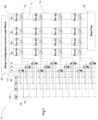
- an electro-optical image acquisition device comprises: a plurality of light-sensing sub-blocks (20), each comprising at least one photosensitive element (80) which comprises a photodetector element for the conversion of light information into an electrical signal and electronic media controllable by reset signals and capable of resetting the relevant photodetector; a detected signal reading block for reading the output signal from the photosensitive elements; row and column selection elements, which enable access to different photosensitive elements of the matrix and their reading by means of the aforementioned detected signal reading block; and pixel discharge control circuitry.
- the pixel discharge control circuits are configured so as to combine a plurality of input voltage signals, to generate one or more reset curves which are transported to the photosensitive elements by means of reset curve distribution lines.
- Said pixel discharge control circuits are configured to generate a plurality of reset curves and to dynamically select, for each photosensitive element, an appropriate reset curve among those available transported by said reset curve distribution lines while storing such a selection until the next selection.
- the pixel discharge control circuits comprise reset curve generation elements configured to allow the selective propagation in succession of the various line-by-line reset curves over time, so as to ensure a high dynamic response even in the event of operation with uncontrolled light.
- the device outlined above allows to obtain zones of the matrix of photosensitive elements with different light dynamics within the scene itself and to obtain so-called "multidynamic" images. This allows to both optimize the quality of the image by enabling an overall dynamic response which can even exceed the dynamics of the individual photosensitive elements and to enable schemes which allow to maximize the information content if the image is subsequently processed by a computer.
- the proposed technique allows to obtain images with a higher number of bits than the native number of the electro-optical sensor by virtue of the application of one or more flags which identify the associated dynamics within the information extracted from each photosensitive element. Such information is used during the reconstruction of the image to increase the contrast of the image as a whole.
- the image thus constructed can then be displayed on HDR monitors or exploited with image processing techniques to optimize the information processing and extraction processes.
- an electro-optical device for the acquisition of digital images 10 comprises: a plurality of light-sensing sub-blocks, 20, arranged in rows and columns to form a matrix structure, which could have any geometry, even linear; elements for generating a reset curve, 30, capable of appropriately combining input voltage signals, 40, available and transported along the entire matrix, so as to generate appropriate reset curves transported by means of reset curve distribution lines 13 to the light-sensing sub-blocks 20.
- input voltage signals 40 can be constants, such as mass, power or other intermediate values generated inside or outside the electro-optical device, or be programmable voltages, such as those generated by digital-analog converters, called DACs.
- the various input voltage signals 40 are brought to the various reset curve generation elements 30 by means of matrix-level voltage signal transport lines 15, and row-level voltage signal transport lines 16.
- the reset curve generation elements 30 act as selectors in that they select, from time to time, one of the input voltage signals 40; however, they can be suitable to perform a combination or alteration of said input voltage signals 40 to generate an appropriate reset curve.
- the device 10 further comprises a control block 50 adapted to generate an appropriate sequence of signals useful to the reset curve generation elements 30 and the light-sensing sub-blocks 20 for generating and propagating the reset voltage within the device in an appropriate manner.
- the aforementioned signals are transmitted from the control block 50 to the reset curve generation elements 30, and to the light-sensing sub-blocks 20, by means of lines of the reset curve generation control signal 12 (hereinafter also referred to simply as control signal lines), and lines of the reset curve selection signal at the pixel level 11, respectively.
- the distribution of the reset curves occurs, by means of the reset curve distribution lines 13, per row, but this is only one implementation example. In fact, it can occur by column or other configuration without thereby departing from the objects of the present invention.
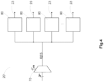
- row and column selection elements are not depicted in the figure because they are known to the state of the art, but are present in that they are necessary for the operation of the device; they enable access to the different photosensitive elements of the matrix and the reading thereof by means of a detected signal reading block 60, whose implementation mode is also known in the state of the art.
- the various light-sensing sub-blocks 20 are connected to the detected signal reading block 60 by means of detected signal reading lines 14.
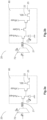
- Each sub-block 20 includes a reset curve selection circuit 70, and a photosensitive element 80, or pixel.
- the photosensitive element 80 has at least one reset terminal 21, one selection terminal 22 and one reading terminal 23.
- the reset terminal 21 is connected to the reset curve selection circuit 70.
- a light-sensing sub-block 20' includes a reset curve selection circuit 70, to which a plurality of photosensitive elements 80 are connected. Within the sub-block 20', the individual photosensitive elements 80 can then be directed independently or in groups for reading the relevant output signal 23.
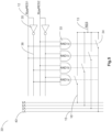
- a reset curve generation element 30 in the device 10 comprises:
- circuits adapted to realize the AND 33, and NOT 35 logic ports are of purely digital type, as well as the switches 34 and can advantageously be implemented in CMOS technology as known in the state of the art.
- the reset curve generation element 30 shown in Fig.5 is an example which allows the management of four input voltage signals 40, indicated with V1, V2, V3 and V4, and directed by the control signals, RowRES1 and RowRES2, corresponding to two lines of the control signal 12, but can be easily extended to a variant of 2 n input voltage signals 40, and n lines of the control signal 12. In such a case, 2 n AND ports 33, n NOT ports 35, and 2 n switches 34 will be required.
- the structure presented in Fig.5 allows to bring the reset curve to all the photosensitive elements of the matrix at the same time and therefore continues to ensure appropriate operation with controlled light.
- the number of input voltage signals 40 constant or programmable, is 2 n , with the number n defined at the implementation step, and consequently the number of lines of the control signal 12, for each reset curve generation element 30, is n to make all the voltages available at the input of the generation blocks 30 accessible.
- the number of reset curves generated and propagated to the various photosensitive elements line by line by means of the reset curve distribution lines 13 is 2 m , as designed, and consequently the number of lines of the selection signal 11 which will go to each light-sensing sub-block 20 is m.
- m 0 (zero)
- the structure composed of 2 m reset curve generation elements 30 is repeated row by row. It is evident that row propagation is only one variant, while other configurations are possible.
- a different group of input voltage signals 40 is associated with each reset curve generation element 30 of a row.
- the structure consisting of m reset curve generation elements 30 is repeated line by line and the various groups of input voltage signals 40 are similarly associated with the m reset curve generation elements 30 of each line.
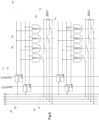
- FIG.6 A variant of a reset curve generation element 30' is shown in Fig.6 .
- This variant represents the next stage with respect to the variant of Fig.5 .
- the input voltage signals 40 are still present, transported by means of the voltage signal transport lines 15 and 16, and the AND ports 33, which allow the combination of the signals 40, as well as the switches 34, which exclusively connect the signal transport lines 16 to two terminals, RES1 and RES2, connecting to respective reset curve distribution lines 13 exiting from the reset curve generation element 30.
- the control signals of the AND ports 33 are generated by flip-flops, 37, and transported by the lines of the ports 32 and 36.
- Such flip-flops 37 are known in the state of the art and in the proposed implementation are repeated per row/sub-block, allowing, in addition to generating the negated signal, the sliding of a signature along the matrix of light-sensing sub-blocks 20 at each clock cycle 39, by means of control signals RowRES1 and RowRES2 transported by the control signal lines 12. Thereby, over time, there will be a delay of a clock cycle 39 in the signal configuration for each row/sub-block, thus realizing the sliding of a certain reset curve along the distribution lines 13, and therefore along the matrix of photosensitive elements 80. This enables the possibility of the sensor to work even in uncontrolled light and in the so-called rolling shutter condition.
- Fig.6 also shows an example with four input voltage signals 40 (V1, V2, V3 and V4) and two control signal lines 12 (RowRES1 and RowRES2 signals) which allow the generation of a reset curve 13 for each row/sub-block, where in this case the number of rows/sub-blocks is equal to two.
- V1, V2, V3 and V4 input voltage signals 40
- RowRES1 and RowRES2 signals two control signal lines 12
- the reset curve selection circuit 70 may not be present and the light-sensing sub-blocks 20 would then comprise only the photosensitive elements 80.
- Fig.7 and Fig.8 use four input voltage signals 40, which correspond to fixed or programmable voltages available within the electro-optical device set at different time points, identified with T1, T2, T3 and T4.
- T1, T2, T3 and T4 the example can be easily extended to 2 n input voltage signals 40 enabled at different time points in a number not necessarily equal to the number of signals. In fact, the different voltage signals available may not all be used or be used multiple times.
- Fig.7 and Fig.8 also show the control signals RowRES1 and RowRES2 transmitted by means of the control signal lines 12 and used for generating the reset curves shown in the graphs and the related conversion tables.
- a selection circuit 70 has a structure similar to that of the reset curve generation element 30' shown in Fig.6 , and this structure is used in the sub-block 20 to select the appropriate reset curve 13 from those transmitted by the reset curve distribution lines 13 associated with the sub-block 20 itself.
- the sub-block-level structure 20 includes a memory element, such as a flip-flop, adapted to maintain the configuration which selects the appropriate reset curve for as long as necessary for the generation and acquisition of an image, i.e., for the integration and reading time, or a multiple thereof.
- the flip-flop structure facilitates matrix programming prior to the image generation and acquisition step by scrolling a programming signature along the different columns, or rows, or sub-blocks of different shapes. It should be noted that the clock 39 of Fig.6 will be different if such a configuration is used to select the appropriate reset curve at the sub-block level 20, i.e., in the selection circuit 70, with respect to what occurs in the reset curve generation element 30, 30'.
- the structure shown in Fig. 6 is only one example of an implementation of the structure usable to implement the selection circuit 70.
- it can be alternatively considered to combine any memory element in the selection circuit 70, the implementation of which is known in the state of the art in the different forms thereof, with a selection element of the single sub-block 20 implemented with a row and column decoder which allows the selection of the single sub-block 20 and the consequent programming thereof.
- Fig. 9 shows an example of signal propagation along the lines, always referring to an example in which there are four input voltage signals 40, two control signal lines, 12, and two rows of sub-blocks for detecting light 20. Thereby, the generated reset curve will slide along the different rows/sub-blocks of the matrix.
- an electro-optical image acquisition device has several advantages with respect to the more common devices of the known art. Firstly, it allows to obtain dynamic images of variable light in any lighting condition, generating a response which can be adapted very precisely to lighting conditions and operator needs. Furthermore, different areas of the matrix of photosensitive elements can be programmed with different light dynamics so as to maximize the information contained in the final image, rather than the information available to the operator and/or the computer to extract useful information. It should be noted that the capillarity of the matrix programming can reach, depending on the implementation choices, even the single pixel or be managed by sub-blocks.
- a light-sensing sub-block 20, consisting of a selection circuit, 70, and a plurality of photosensitive elements 80 associated therewith could comprise not all of the photosensitive elements 80 of a row but any number of pixels 80 with any arrangement in the matrix; and the device 10 could comprise a plurality of light-sensing sub-blocks 20, not identical to each other, i.e., composed of different numbers of pixels 80.
Landscapes
- Engineering & Computer Science (AREA)
- Multimedia (AREA)
- Signal Processing (AREA)
- Physics & Mathematics (AREA)
- Nonlinear Science (AREA)
- Transforming Light Signals Into Electric Signals (AREA)
- Facsimile Heads (AREA)
- Solid State Image Pick-Up Elements (AREA)
Claims (9)
- Elektro-optische Bilderfassungsvorrichtung (10) die folgendes aufweist:- eine Vielzahl von Lichtsensor-Unterblöcken (20), die jeweils mindestens ein lichtempfindliches Element (80) umfassen, das ein Fotodetektorelement zur Umwandlung von Lichtinformationen in ein elektrisches Signal und elektronische Medien enthält, die durch Rücksetzsignale steuerbar sind und den betreffenden Fotodetektor zurücksetzen können;- einen Block (60) zum Lesen des detektierten Signals, der dazu dient, das Ausgangssignal von den lichtempfindlichen Elementen (80) zu lesen;- Zeilen- und Spaltenauswahlelemente, die den Zugriff auf verschiedene lichtempfindliche Elemente (80) der Vorrichtung und deren Auslesen mittels des Blocks (60) zum Lesen des erfassten Signals ermöglichen; und- Pixelentladungs-Steuerschaltungen;wobei die Pixelentladungssteuerschaltungen so konfiguriert sind, dass sie eine Vielzahl von Eingangsspannungssignalen (40) kombinieren, um mindestens eine Rücksetzkurve zu erzeugen, die durch mindestens eine Rücksetzkurvenverteilungsleitung (13) zu einem oder mehreren der Lichtsensor-Unterblöcken (20) transportiert wird,dadurch gekennzeichnet, dass die Pixelentladungs-Steuerschaltungen Folgendes umfassen:- Rücksetzkurven-Erzeugungselemente (30), die dafür ausgelegt sind, die Eingangsspannungssignale (40) zu kombinieren, um eine definierte Anzahl von Rücksetzkurven zu erzeugen,- mindestens einen Steuerblock (50), der geeignet ist, eine geeignete Folge von Signalen zu erzeugen, die für die Rücksetzkurven-Erzeugungselemente (30) nützlich sind, um die Rücksetzkurven innerhalb der Vorrichtung (10) auf geeignete Weise zu erzeugen und weiterzuleiten;wobei jedes der Rücksetzkurven-Erzeugungselemente (30) Folgendes umfasst:- AND-Ports (33), die Schalter (34) steuern, die auf den Spannungssignaltransportleitungen (16) vorhanden sind, und die ausschließlich die Eingangsspannungssignale (40) mit einer Verteilungsleitung der Rückstellkurve (13) verbinden, die von dem Rückstellkurven-Erzeugungselement (30) ausgeht:- NOT-Ports (35) zur Erzeugung eines negierten Signals (36) aus dem Signal der Signalsteuerleitungen (12), so dass das Signal der Signalsteuerleitungen (12) und das zugehörige negierte Signal (36) den Eingang der AND-Ports (33) bilden.
- Elektro-optische Bilderfassungsvorrichtung (10) nach Anspruch 1, dadurch gekennzeichnet, dass die Pixelentladungs-Steuerschaltungen so ausgelegt sind, dass sie eine Vielzahl von Rücksetzkurven erzeugen und für jeden der Lichtsensor-Unterblöcken (20) dynamisch eine geeignete Rücksetzkurve unter den verfügbaren auswählen, die von den Verteilungsleitungen der Rücksetzkurven (13) transportiert werden, während sie diese Auswahl bis zur nächsten Auswahl speichern.
- Elektro-optische Vorrichtung nach Anspruch 2, dadurch gekennzeichnet, dass mindestens einer der Lichtsensor-Unterblöcken (20) eine Rückstellkurven-Auswahlschaltung (70) umfasst, die mit einer Vielzahl von lichtempfindlichen Elementen (80) verbunden ist.
- Elektro-optische Bilderfassungsvorrichtung (10) nach Anspruch 2, dadurch gekennzeichnet, dass die Pixelentladungs-Steuerschaltungen Folgendes umfassen:- Rücksetzkurven-Auswahlschaltungen (70), die jeweils mindestens einem der lichtempfindlichen Elemente (80) zugeordnet sind, um einen Lichterfassungs-Unterblock (20) zu bilden, wobei die Rücksetzkurven-Auswahlschaltungen (70) so konfiguriert sind, dass sie aus einer Vielzahl von Rücksetzkurven, die über eine entsprechende Vielzahl von Rücksetzkurven-Verteilungsleitungen (13) empfangen werden, eine geeignete Rücksetzkurve unter denjenigen auswählen, die über die Rücksetzkurven-Verteilungsleitungen (13) verfügbar sind, und diese Auswahl bis zu einer späteren Auswahl speichern;- mindestens einen Steuerblock (50), der geeignet ist, eine geeignete Folge von Signalen zu erzeugen, die für die Rückstellkurven-Erzeugungselemente (30) nützlich sind, um eine geeignete Rückstellkurve unter denjenigen auszuwählen, die durch die Rückstellkurven-Verteilungsleitungen (13) übertragen werden.
- Elektro-optische Bilderfassungsvorrichtung (10) nach Anspruch 1, dadurch gekennzeichnet, dass die Steuerschaltung für die Pixelentladung Elemente für die Erzeugung der Rückstellkurven (30') enthält, die für die selektive Ausbreitung verschiedener Rückstellkurven Zeile für Zeile im Laufe der Zeit ausgelegt sind, um eine hohe Dynamik auch im Falle eines unkontrollierten Lichtbetriebs zu gewährleisten.
- Elektro-optische Bilderfassungsvorrichtung (10) nach Anspruch 1, dadurch gekennzeichnet, dass jedes der Erzeugungselemente zur Erzeugung der Rücksetzkurven (30') Flip-Flops (37) umfasst, die so ausgelegt sind, dass sie Steuersignale, die von den Signalsteuerleitungen (12) übertragen werden, und ein Taktsignal (39) empfangen, um Steuersignale der AND-Ports (33) zu erzeugen, so dass zusätzlich zur Erzeugung des negierten Signals bei jedem Taktzyklus (39) das Scrollen einer Signatur entlang der Lichtsensor-Unterblöcke (20) ermöglicht wird.
- Elektro-optische Bilderfassungsvorrichtung (10) nach dem vorhergehenden Anspruch, dadurch gekennzeichnet, dass jede der Auswahlschaltungen zur Auswahl der Rücksetzkurve (70) eine Struktur analog zu derjenigen der Erzeugungselemente zur Erzeugung der Rücksetzkurven (30') aufweist, wobei eine solche Struktur in dem jeweiligen lichtempfindlichen Unterblock (20) verwendet wird, um die geeignete Rücksetzkurve unter denjenigen auszuwählen, die von den dem Unterblock (20) selbst zugeordneten Rücksetzkurven-Verteilungsleitungen (13) übertragen werden, wobei die Schaltung (70) zur Auswahl der Rückstellkurve ein Speicherelement enthält, das geeignet ist, die Konfiguration beizubehalten, die die geeignete Rückstellkurve für die gesamte für die Erzeugung und Erfassung eines Bildes notwendige Zeit, d.h. für die Zeit der Integration und des Lesens, oder ein Vielfaches davon, auswählt.
- Elektro-optische Bilderfassungsvorrichtung (10) nach Anspruch 1, dadurch gekennzeichnet, dass die logischen Ports AND (33) und NOT (35) und die Schalter (34) rein digitaler Art in CMOS-Technologie sind.
- Elektro-optische Bilderfassungsvorrichtung (10') nach Anspruch 3, dadurch gekennzeichnet, dass die lichterfassenden Unterblöcke (20) in Zeilen und Spalten angeordnet sind, um eine Matrixstruktur zu bilden, wobei jedem Rücksetzkurven-Erzeugungselement (30) einer Zeile eine andere Gruppe von Eingangsspannungssignalen (40) zugeordnet ist, wobei eine Struktur, die aus einer Vielzahl von Rücksetzkurven-Erzeugungselementen (30) besteht, zeilenweise wiederholt wird und die verschiedenen Gruppen von Eingangsspannungssignalen (40) den Rücksetzkurven-Erzeugungselementen (30) jeder Zeile auf ähnliche Weise zugeordnet sind.
Applications Claiming Priority (2)
| Application Number | Priority Date | Filing Date | Title |
|---|---|---|---|
| IT202000011380 | 2020-05-18 | ||
| PCT/IB2021/054268 WO2021234566A1 (en) | 2020-05-18 | 2021-05-18 | Multidynamics vision sensor |
Publications (3)
| Publication Number | Publication Date |
|---|---|
| EP4154517A1 EP4154517A1 (de) | 2023-03-29 |
| EP4154517C0 EP4154517C0 (de) | 2024-11-13 |
| EP4154517B1 true EP4154517B1 (de) | 2024-11-13 |
Family
ID=71994859
Family Applications (1)
| Application Number | Title | Priority Date | Filing Date |
|---|---|---|---|
| EP21733536.3A Active EP4154517B1 (de) | 2020-05-18 | 2021-05-18 | Multidynamischer bilddetektor |
Country Status (2)
| Country | Link |
|---|---|
| EP (1) | EP4154517B1 (de) |
| WO (1) | WO2021234566A1 (de) |
Families Citing this family (2)
| Publication number | Priority date | Publication date | Assignee | Title |
|---|---|---|---|---|
| WO2025243215A1 (en) | 2024-05-21 | 2025-11-27 | Eye-Tech S.R.L. | Method for controlling the discharge of a photosensitive element in a photodetector and photodetector thereof |
| CN118566668B (zh) * | 2024-06-20 | 2025-07-04 | 清华大学深圳国际研究生院 | 设备局部放电监测方法及装置、电子设备及存储介质 |
Citations (4)
| Publication number | Priority date | Publication date | Assignee | Title |
|---|---|---|---|---|
| US20020043610A1 (en) * | 2000-07-28 | 2002-04-18 | Smal Camera Technologies, Inc. | Precise MOS imager transfer function control for expanded dynamic range imaging |
| US20050167602A1 (en) * | 1998-02-09 | 2005-08-04 | Bart Dierickx | Imaging device having a pixel structure with high dynamic range read-out signal |
| US20070216789A1 (en) * | 2006-03-15 | 2007-09-20 | Honeywell International, Inc. | System and apparatus for high dynamic range sensor |
| US20170251151A1 (en) * | 2016-02-26 | 2017-08-31 | Intel Corporation | Image sensor operation for shutter modulation and high dynamic range |
-
2021
- 2021-05-18 WO PCT/IB2021/054268 patent/WO2021234566A1/en not_active Ceased
- 2021-05-18 EP EP21733536.3A patent/EP4154517B1/de active Active
Patent Citations (4)
| Publication number | Priority date | Publication date | Assignee | Title |
|---|---|---|---|---|
| US20050167602A1 (en) * | 1998-02-09 | 2005-08-04 | Bart Dierickx | Imaging device having a pixel structure with high dynamic range read-out signal |
| US20020043610A1 (en) * | 2000-07-28 | 2002-04-18 | Smal Camera Technologies, Inc. | Precise MOS imager transfer function control for expanded dynamic range imaging |
| US20070216789A1 (en) * | 2006-03-15 | 2007-09-20 | Honeywell International, Inc. | System and apparatus for high dynamic range sensor |
| US20170251151A1 (en) * | 2016-02-26 | 2017-08-31 | Intel Corporation | Image sensor operation for shutter modulation and high dynamic range |
Also Published As
| Publication number | Publication date |
|---|---|
| WO2021234566A1 (en) | 2021-11-25 |
| EP4154517A1 (de) | 2023-03-29 |
| EP4154517C0 (de) | 2024-11-13 |
Similar Documents
| Publication | Publication Date | Title |
|---|---|---|
| CN102625059B (zh) | 用于移动式应用的cmos图像传感器的动态范围扩展 | |
| KR101348522B1 (ko) | 고체 촬상 장치 및 거리 화상 측정 장치 | |
| CN102238345B (zh) | 具有减少的列固定图案噪声的成像传感器 | |
| EP4154517B1 (de) | Multidynamischer bilddetektor | |
| KR101188598B1 (ko) | 화상 처리 방법, 물리량 분포 검출용 반도체 장치 및 전자 기기 | |
| KR20080067963A (ko) | 고체 상태 촬상 장치 및 촬상 장치 | |
| US11190717B2 (en) | Solid state image sensor, image capturing apparatus, and image capturing method | |
| JP2023545370A (ja) | 量子化動作を低減したデジタル画素センサ | |
| JP2023506277A (ja) | 錐体及び桿体のバイモーダル生体模倣視覚センサ | |
| EP3185541A1 (de) | Bildsensorkonfiguration | |
| CN116052598B (zh) | 显示装置及其驱动方法 | |
| DE102020103858A1 (de) | Biometrische signalmessvorrichtung | |
| Zhang et al. | A closed-loop, all-electronic pixel-wise adaptive imaging system for high dynamic range videography | |
| KR100657145B1 (ko) | 스케일러를 구비한 이미지센서 및 이미지센서의 이미지 스케일링 방법 | |
| CN113035112B (zh) | 显示面板的驱动方法、驱动芯片及显示装置 | |
| JP7116620B2 (ja) | 撮像素子及び撮像装置 | |
| KR100569734B1 (ko) | 프로그램 가능한 감마 기준전압 발생회로 및 이를 이용한 액정표시 장치 | |
| US5030947A (en) | Device to generate brilliance levels on a display screen | |
| US5856666A (en) | Multiplexer circuit | |
| KR101653622B1 (ko) | 엣지 정보 추출을 위한 이미지 센서 | |
| JP2023053350A (ja) | 光電変換装置および撮像システム | |
| KR101444014B1 (ko) | 이미지 센서의 구동 회로 및 구동 방법 | |
| CN112750401A (zh) | 显示驱动装置及方法 | |
| CN112600996B (zh) | 紫外仿生视觉传感器 | |
| JP4322562B2 (ja) | 固体撮像装置 |
Legal Events
| Date | Code | Title | Description |
|---|---|---|---|
| STAA | Information on the status of an ep patent application or granted ep patent |
Free format text: STATUS: UNKNOWN |
|
| STAA | Information on the status of an ep patent application or granted ep patent |
Free format text: STATUS: THE INTERNATIONAL PUBLICATION HAS BEEN MADE |
|
| PUAI | Public reference made under article 153(3) epc to a published international application that has entered the european phase |
Free format text: ORIGINAL CODE: 0009012 |
|
| STAA | Information on the status of an ep patent application or granted ep patent |
Free format text: STATUS: REQUEST FOR EXAMINATION WAS MADE |
|
| 17P | Request for examination filed |
Effective date: 20221212 |
|
| AK | Designated contracting states |
Kind code of ref document: A1 Designated state(s): AL AT BE BG CH CY CZ DE DK EE ES FI FR GB GR HR HU IE IS IT LI LT LU LV MC MK MT NL NO PL PT RO RS SE SI SK SM TR |
|
| DAV | Request for validation of the european patent (deleted) | ||
| DAX | Request for extension of the european patent (deleted) | ||
| REG | Reference to a national code |
Ref country code: DE Ref legal event code: R079 Free format text: PREVIOUS MAIN CLASS: H04N0005355000 Ipc: H04N0025571000 Ref document number: 602021021800 Country of ref document: DE |
|
| GRAP | Despatch of communication of intention to grant a patent |
Free format text: ORIGINAL CODE: EPIDOSNIGR1 |
|
| STAA | Information on the status of an ep patent application or granted ep patent |
Free format text: STATUS: GRANT OF PATENT IS INTENDED |
|
| RIC1 | Information provided on ipc code assigned before grant |
Ipc: H04N 25/779 20230101ALI20240503BHEP Ipc: H04N 25/77 20230101ALI20240503BHEP Ipc: H04N 25/709 20230101ALI20240503BHEP Ipc: H04N 25/571 20230101AFI20240503BHEP |
|
| INTG | Intention to grant announced |
Effective date: 20240612 |
|
| GRAS | Grant fee paid |
Free format text: ORIGINAL CODE: EPIDOSNIGR3 |
|
| GRAA | (expected) grant |
Free format text: ORIGINAL CODE: 0009210 |
|
| STAA | Information on the status of an ep patent application or granted ep patent |
Free format text: STATUS: THE PATENT HAS BEEN GRANTED |
|
| AK | Designated contracting states |
Kind code of ref document: B1 Designated state(s): AL AT BE BG CH CY CZ DE DK EE ES FI FR GB GR HR HU IE IS IT LI LT LU LV MC MK MT NL NO PL PT RO RS SE SI SK SM TR |
|
| REG | Reference to a national code |
Ref country code: GB Ref legal event code: FG4D |
|
| REG | Reference to a national code |
Ref country code: CH Ref legal event code: EP |
|
| REG | Reference to a national code |
Ref country code: IE Ref legal event code: FG4D |
|
| REG | Reference to a national code |
Ref country code: DE Ref legal event code: R096 Ref document number: 602021021800 Country of ref document: DE |
|
| U01 | Request for unitary effect filed |
Effective date: 20241118 |
|
| U07 | Unitary effect registered |
Designated state(s): AT BE BG DE DK EE FI FR IT LT LU LV MT NL PT RO SE SI Effective date: 20241128 |
|
| PG25 | Lapsed in a contracting state [announced via postgrant information from national office to epo] |
Ref country code: IS Free format text: LAPSE BECAUSE OF FAILURE TO SUBMIT A TRANSLATION OF THE DESCRIPTION OR TO PAY THE FEE WITHIN THE PRESCRIBED TIME-LIMIT Effective date: 20250313 Ref country code: HR Free format text: LAPSE BECAUSE OF FAILURE TO SUBMIT A TRANSLATION OF THE DESCRIPTION OR TO PAY THE FEE WITHIN THE PRESCRIBED TIME-LIMIT Effective date: 20241113 |
|
| PG25 | Lapsed in a contracting state [announced via postgrant information from national office to epo] |
Ref country code: ES Free format text: LAPSE BECAUSE OF FAILURE TO SUBMIT A TRANSLATION OF THE DESCRIPTION OR TO PAY THE FEE WITHIN THE PRESCRIBED TIME-LIMIT Effective date: 20241113 |
|
| PG25 | Lapsed in a contracting state [announced via postgrant information from national office to epo] |
Ref country code: NO Free format text: LAPSE BECAUSE OF FAILURE TO SUBMIT A TRANSLATION OF THE DESCRIPTION OR TO PAY THE FEE WITHIN THE PRESCRIBED TIME-LIMIT Effective date: 20250213 |
|
| PG25 | Lapsed in a contracting state [announced via postgrant information from national office to epo] |
Ref country code: GR Free format text: LAPSE BECAUSE OF FAILURE TO SUBMIT A TRANSLATION OF THE DESCRIPTION OR TO PAY THE FEE WITHIN THE PRESCRIBED TIME-LIMIT Effective date: 20250214 |
|
| PG25 | Lapsed in a contracting state [announced via postgrant information from national office to epo] |
Ref country code: PL Free format text: LAPSE BECAUSE OF FAILURE TO SUBMIT A TRANSLATION OF THE DESCRIPTION OR TO PAY THE FEE WITHIN THE PRESCRIBED TIME-LIMIT Effective date: 20241113 |
|
| PG25 | Lapsed in a contracting state [announced via postgrant information from national office to epo] |
Ref country code: RS Free format text: LAPSE BECAUSE OF FAILURE TO SUBMIT A TRANSLATION OF THE DESCRIPTION OR TO PAY THE FEE WITHIN THE PRESCRIBED TIME-LIMIT Effective date: 20250213 |
|
| U20 | Renewal fee for the european patent with unitary effect paid |
Year of fee payment: 5 Effective date: 20250519 |
|
| PG25 | Lapsed in a contracting state [announced via postgrant information from national office to epo] |
Ref country code: SM Free format text: LAPSE BECAUSE OF FAILURE TO SUBMIT A TRANSLATION OF THE DESCRIPTION OR TO PAY THE FEE WITHIN THE PRESCRIBED TIME-LIMIT Effective date: 20241113 |
|
| PG25 | Lapsed in a contracting state [announced via postgrant information from national office to epo] |
Ref country code: SK Free format text: LAPSE BECAUSE OF FAILURE TO SUBMIT A TRANSLATION OF THE DESCRIPTION OR TO PAY THE FEE WITHIN THE PRESCRIBED TIME-LIMIT Effective date: 20241113 |
|
| PG25 | Lapsed in a contracting state [announced via postgrant information from national office to epo] |
Ref country code: CZ Free format text: LAPSE BECAUSE OF FAILURE TO SUBMIT A TRANSLATION OF THE DESCRIPTION OR TO PAY THE FEE WITHIN THE PRESCRIBED TIME-LIMIT Effective date: 20241113 |
|
| RAP4 | Party data changed (patent owner data changed or rights of a patent transferred) |
Owner name: EYE-TECH S.R.L. |
|
| U1H | Name or address of the proprietor changed after the registration of the unitary effect |
Owner name: EYE-TECH S.R.L.; IT |
|
| PLBE | No opposition filed within time limit |
Free format text: ORIGINAL CODE: 0009261 |
|
| STAA | Information on the status of an ep patent application or granted ep patent |
Free format text: STATUS: NO OPPOSITION FILED WITHIN TIME LIMIT |
|
| 26N | No opposition filed |
Effective date: 20250814 |
|
| REG | Reference to a national code |
Ref country code: CH Ref legal event code: H13 Free format text: ST27 STATUS EVENT CODE: U-0-0-H10-H13 (AS PROVIDED BY THE NATIONAL OFFICE) Effective date: 20251223 |
|
| PG25 | Lapsed in a contracting state [announced via postgrant information from national office to epo] |
Ref country code: CH Free format text: LAPSE BECAUSE OF NON-PAYMENT OF DUE FEES Effective date: 20250531 |
|
| GBPC | Gb: european patent ceased through non-payment of renewal fee |
Effective date: 20250518 |
|
| PG25 | Lapsed in a contracting state [announced via postgrant information from national office to epo] |
Ref country code: MC Free format text: LAPSE BECAUSE OF FAILURE TO SUBMIT A TRANSLATION OF THE DESCRIPTION OR TO PAY THE FEE WITHIN THE PRESCRIBED TIME-LIMIT Effective date: 20241113 |