EP4154180B1 - Verfahren zur elektrochemischen metallisierung einer doppelseitigen elektrischen schaltung für eine chipkarte und mit diesem verfahren hergestellte elektrische schaltung - Google Patents
Verfahren zur elektrochemischen metallisierung einer doppelseitigen elektrischen schaltung für eine chipkarte und mit diesem verfahren hergestellte elektrische schaltung Download PDFInfo
- Publication number
- EP4154180B1 EP4154180B1 EP21725219.6A EP21725219A EP4154180B1 EP 4154180 B1 EP4154180 B1 EP 4154180B1 EP 21725219 A EP21725219 A EP 21725219A EP 4154180 B1 EP4154180 B1 EP 4154180B1
- Authority
- EP
- European Patent Office
- Prior art keywords
- antenna
- connection
- chip
- electrical circuit
- contacts
- Prior art date
- Legal status (The legal status is an assumption and is not a legal conclusion. Google has not performed a legal analysis and makes no representation as to the accuracy of the status listed.)
- Active
Links
Images


Classifications
-
- G—PHYSICS
- G06—COMPUTING OR CALCULATING; COUNTING
- G06K—GRAPHICAL DATA READING; PRESENTATION OF DATA; RECORD CARRIERS; HANDLING RECORD CARRIERS
- G06K19/00—Record carriers for use with machines and with at least a part designed to carry digital markings
- G06K19/06—Record carriers for use with machines and with at least a part designed to carry digital markings characterised by the kind of the digital marking, e.g. shape, nature, code
- G06K19/067—Record carriers with conductive marks, printed circuits or semiconductor circuit elements, e.g. credit or identity cards also with resonating or responding marks without active components
- G06K19/07—Record carriers with conductive marks, printed circuits or semiconductor circuit elements, e.g. credit or identity cards also with resonating or responding marks without active components with integrated circuit chips
- G06K19/077—Constructional details, e.g. mounting of circuits in the carrier
- G06K19/07749—Constructional details, e.g. mounting of circuits in the carrier the record carrier being capable of non-contact communication, e.g. constructional details of the antenna of a non-contact smart card
- G06K19/07766—Constructional details, e.g. mounting of circuits in the carrier the record carrier being capable of non-contact communication, e.g. constructional details of the antenna of a non-contact smart card comprising at least a second communication arrangement in addition to a first non-contact communication arrangement
- G06K19/07769—Constructional details, e.g. mounting of circuits in the carrier the record carrier being capable of non-contact communication, e.g. constructional details of the antenna of a non-contact smart card comprising at least a second communication arrangement in addition to a first non-contact communication arrangement the further communication means being a galvanic interface, e.g. hybrid or mixed smart cards having a contact and a non-contact interface
-
- G—PHYSICS
- G06—COMPUTING OR CALCULATING; COUNTING
- G06K—GRAPHICAL DATA READING; PRESENTATION OF DATA; RECORD CARRIERS; HANDLING RECORD CARRIERS
- G06K19/00—Record carriers for use with machines and with at least a part designed to carry digital markings
- G06K19/06—Record carriers for use with machines and with at least a part designed to carry digital markings characterised by the kind of the digital marking, e.g. shape, nature, code
- G06K19/067—Record carriers with conductive marks, printed circuits or semiconductor circuit elements, e.g. credit or identity cards also with resonating or responding marks without active components
- G06K19/07—Record carriers with conductive marks, printed circuits or semiconductor circuit elements, e.g. credit or identity cards also with resonating or responding marks without active components with integrated circuit chips
- G06K19/077—Constructional details, e.g. mounting of circuits in the carrier
- G06K19/0772—Physical layout of the record carrier
- G06K19/07722—Physical layout of the record carrier the record carrier being multilayered, e.g. laminated sheets
-
- G—PHYSICS
- G06—COMPUTING OR CALCULATING; COUNTING
- G06K—GRAPHICAL DATA READING; PRESENTATION OF DATA; RECORD CARRIERS; HANDLING RECORD CARRIERS
- G06K19/00—Record carriers for use with machines and with at least a part designed to carry digital markings
- G06K19/06—Record carriers for use with machines and with at least a part designed to carry digital markings characterised by the kind of the digital marking, e.g. shape, nature, code
- G06K19/067—Record carriers with conductive marks, printed circuits or semiconductor circuit elements, e.g. credit or identity cards also with resonating or responding marks without active components
- G06K19/07—Record carriers with conductive marks, printed circuits or semiconductor circuit elements, e.g. credit or identity cards also with resonating or responding marks without active components with integrated circuit chips
- G06K19/077—Constructional details, e.g. mounting of circuits in the carrier
- G06K19/07749—Constructional details, e.g. mounting of circuits in the carrier the record carrier being capable of non-contact communication, e.g. constructional details of the antenna of a non-contact smart card
- G06K19/07773—Antenna details
- G06K19/07794—Antenna details the record carrier comprising a booster or auxiliary antenna in addition to the antenna connected directly to the integrated circuit
Definitions
- the invention relates to the field of smart cards and more particularly to the field of electronic modules for smart cards.
- Smart cards have multiple uses: credit cards, SIM cards for mobile phones, transport cards, identity cards, etc.
- These cards generally consist of a rigid support, for example made of plastic, constituting the main part of the card, in which is incorporated an electronic module manufactured separately.
- This electronic module comprises for example a flexible electrical circuit provided with an electronic chip (integrated circuit) and means for connecting the chip to a device for reading and/or writing data recorded in the chip.
- the invention relates in particular to the field of so-called “Dual” cards, i.e. cards having a double communication interface with the chip. In other words, these cards allow communication with or without contacts. They are also called “Combi” cards.
- the contacts are connected to the chip and are flush on one side of the module to allow an electrical connection to the reading and/or writing device, when the card is inserted into this device.
- an antenna arranged in the card holder (also called card body) is electrically connected to the chip.
- the chip can exchange data with a reading/writing device, either by making a direct electrical connection between the reading/writing device and the contacts of the module, or by making a direct electromagnetic coupling between the antenna and the reading/writing device.
- a first antenna called a “module antenna” is integrated into the module and allows electromagnetic coupling, by inductive coupling (therefore without electrical connection) with a second antenna, called a “booster or master antenna", incorporated in the rigid support of the card mentioned above.
- the first antenna is smaller than the second antenna.
- the second antenna can cover a larger area on the card than that of the module. This makes it possible to obtain a greater communication range.
- the chip can exchange data with a reading/writing device, either by making a direct electrical connection between the reading/writing device and the contacts of the module, or by making an electromagnetic coupling between the module antenna and the booster antenna on the one hand, and the booster antenna and the reading/writing device on the other hand.
- the module antenna communicates (with a resonance effect) in fact thus with a contactless reading and/or writing device, via the booster antenna. So the only physical connections in this second type of Dual cards are at the module level, between the chip and the contacts and between the chip and the module antenna. All these connections are made on the module. This avoids having to make an electrical connection between the antenna incorporated in the card body and the chip incorporated in the module.
- modules comprising a flexible electrical circuit with a front face supporting contacts and a back face supporting the chip and the module antenna. Holes (also called “wells” or “vias”) are then made in the electrical circuit, then the internal wall of these holes is metallized to electrically connect the front and back faces of the module and thus connect the contacts to the chip and to the two ends of the module antenna.
- the antenna In order to facilitate the integration of the module into the card, the antenna must be contained in a module whose dimensions are defined by the ISO 7816-2 standard. Within these dimensions, it is necessary to provide on the rear face of the module an area for placing the chip, areas for the metallized holes, an area with bonding pads or solder pads (also called “bonding pads” in English terminology) for connecting the chip to the contacts and the antenna. In addition, the antenna turns must be made in sufficient number, with a certain width and with a minimum distance between the turns to obtain the desired electromagnetic characteristics.
- connection pads Furthermore, in order to establish, on the connection pads, a reliable and sufficiently low-resistance weld, of the connection wires which electrically connect these connection pads to the chip, it is necessary, on these connection pads, to have one or more metal layers, of sufficient thickness.
- these metal layers are deposited electrochemically, and the current necessary for the electrochemical deposition is supplied by current leads located on the front face (see the document FR3006549 A1 ), the connection pads dedicated to connecting the chip to the contacts are supplied with current via the contacts and the metallized holes.
- connection pads dedicated to connecting the chip to the antenna can also be supplied by the front face via the current leads, possibly a conductive track on the front face having the shape of a tab ("strap" in English) and/or contacts not used for connection with a contact reading and/or writing device, and at least for one of them by the turns of the antenna.
- the current required for electrochemical deposition passes through the antenna turns, relatively large inhomogeneities are observed between, on the one hand, the thickness of the metal layers electrodeposited on the pads dedicated to connecting the chip to the contacts and, on the other hand, the thickness of the metal layers electrodeposited on the pad(s) dedicated to connecting the chip to the antenna and powered via the antenna turns. It also follows that in order to obtain a sufficient thickness of the metal layers electrodeposited on the latter, the deposition time must be considerably increased.
- a method for electrochemical metallization of a double-sided electrical circuit for a smart card communicating with and without contact in which a flexible dielectric substrate is provided having a front face and a rear face. Contacts and current leads electrically connected to at least some of the contacts are arranged on the front face. Connection pads and an antenna are arranged on the rear face. These connection pads are dedicated, for some, to the connection of a chip to the contacts, and for others, to the connection of the chip to the antenna.
- At least one layer of electrically conductive material is deposited by an electrochemical deposition operation at least on some of the connection pads, by supplying these connection pads with current via the current leads, contacts and metallized holes establishing electrical continuity between the front face and the rear face.
- this method comprises, after the electrochemical deposition operation of at least one layer of electrically conductive material, an operation consisting in electrically isolating a metallized hole (i.e. at least one of the additional metallized holes mentioned above), from a connection pad dedicated to the connection of the chip to the antenna.
- a metallized hole i.e. at least one of the additional metallized holes mentioned above
- the additional metallized hole it is possible to supply current to a connection pad dedicated to the connection of the chip to the antenna, directly from the front face and without going through the turns of the antenna. But the use of this additional metallized hole is temporary (during the electrochemical deposition operation). This additional metallized hole is no longer used in the finalized module produced from the electrical circuit obtained by the process according to the invention.
- the invention relates to a double-sided electrical circuit for a smart card communicating with and without contact.
- This circuit comprises a flexible dielectric substrate, with a front face and a back face. Contacts and current leads are located on the front face. An antenna and bonding pads are located on the backside. Some of the bonding pads are dedicated to connecting a chip to the contacts and others are dedicated to connecting the chip to the antenna.
- this circuit includes at least one contact closing at least two plated holes. One of these plated holes is connected to a contact bonding pad dedicated to connecting the chip to this contact. The other of these plated holes is electrically isolated from an antenna bonding pad dedicated to connecting the chip to the antenna. It is not used for electrical conduction during operational use of the electrical circuit in a module.
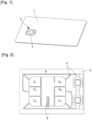
- a smart card 1 communicating with and without contact comprises a module 2.
- a module 2 comprises in particular an electrical circuit 3 and a chip 100 (not visible on the figure 1 ).
- Module 2 is made as a separate element which is inserted into a cavity provided in the body of card 1.
- a booster antenna (not shown) is integrated into the body of card 1 in a known manner.
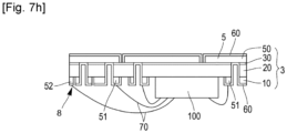
- the electrical circuit 3 comprises several contacts 5 to which the chip 100 is connected (see figure 7H ).
- the electrical circuit 3 is shown in the figure 2 , by its front face 6 (contact face). It is also represented on the figure 3 seen from its rear face 7 (bonding face).
- the electrical circuit 3 shown on the figures 2 And 3 corresponds to a double-sided printed circuit for a “dual” card, with contacts 5 on the front face 6 and an antenna 8 on the rear face 7.
- only a portion of the electrical circuit is shown in the figures. This portion essentially corresponds to that necessary for the production of a module 2.
- Several similar portions can be supported by the same flexible substrate, for example for a continuous implementation of the method according to the invention (i.e. in "reel-to-reel” or "roll-to-roll” in English).
- the contacts 5 are for example six in number: C1, C2, C3, C5, C6 and C7.
- Contact C1 is used for a connection to the positive power-on terminal of the chip 100.
- Contact C2 is used for a connection to the reset terminal of the chip 100.
- Contact C3 is used for a connection to the clock signal terminal of the chip 100.
- Contact C5 is used for a connection to the ground terminal of the chip 100.
- Contact C6 is not directly connected to the chip 100, in the applications targeted by the invention.
- Contact C7 is used for a connection to the input/output terminal of the chip 100.
- each of the contacts C1, C2, C3, C5 and C7 is therefore respectively connected to a terminal of the chip 100, via a metallized hole 40, a contact connection pad 51 (i.e. dedicated to the connection of a contact to the chip) and by an electrically conductive wire 70 connecting a contact connection pad 51 to a terminal of the chip 100 (see Fig. 7h ).
- a contact connection pad 51 i.e. dedicated to the connection of a contact to the chip
- an electrically conductive wire 70 connecting a contact connection pad 51 to a terminal of the chip 100
- FIG. 7h On the figure 3 are identified by C'1, C'2, C'3, C'5 and C'7 the connection pads 51 each respectively connected to a contact 5 (respectively C1, C2, C3, C5 or C7), by means of a metallized hole 40.
- Figures 4 and 3 are not to the same scale.
- figure 3 is actually mirrored (which is on the right in the figure 3 corresponds to what is on the left on the figure 2 and should therefore be to the left and vice versa) of the actual configuration in order to facilitate the identification of the contact connection pads 51 (C'1, C'2, C'3, C'5 and C'7) relative to the contacts 5 (C1, C2, C3, C5 and C7) as shown in the figure 2 .
- these metallized holes 40 serve both to connect, in the finalized module 2, a contact 5 to a contact connection pad 51 and to a terminal of the chip 100, but they are also used during the operation(s) of electrochemical metallization to allow one or more layers of electrically conductive material 60 (for example nickel and gold) to be deposited on these contact connection pads 51.
- electrically conductive material 60 for example nickel and gold
- the chip must also be connected to each of the two ends of the antenna 8.
- two internal and external antenna connection pads 52 i.e. dedicated to the connection of the antenna 8 to the chip 100
- the antenna 8 comprises several turns wound around a central zone corresponding to a fixing zone of the chip 100.
- all the contact 51 and antenna 52 connection pads are located around this central zone, inside the turns of the antenna 8.
- the current leads 4 are conductive tracks which make it possible to establish an electrical connection between an electrode of an electroplating cell and the contacts 5.
- the external antenna connection pad 52 is connected to the external end 81 of the antenna 8 via two metallized holes 40 and a conductive track 9 connecting, on the front face 6, these two metallized holes 40.
- This conductive track 9 is of course itself connected to a current supply 4.
- This conductive track 9 is present in the embodiment described in relation to the figures 2 And 3 , but may be removed and replaced by a contact 5 or a portion of contact 5 according to other embodiments.
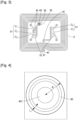
- the internal antenna connection pad 52 is connected to the internal end 82 of the antenna 8 and to the contact C5 by a metallized hole 40I (on the figure 3 this metallized hole 40I is shown already electrically isolated from the internal antenna connection pad 52, but during the metallization phase, it is well connected to it).
- this contact C5 is used in the finalized module 2 for grounding
- this metallized hole 40I is electrically isolated from the internal antenna connection pad 52, for example by releasing, using a laser beam, an insulating ring 90, on the rear face 7 around this metallized hole 40I.
- An enlargement of this region including the metallized hole 40I is shown in the figure 4 .
- the laser beam was moved over the surface of a conductive area connecting the metallized hole 401 to the internal antenna connection pad 52, without leaving this surface, all around this metallized hole 401.
- the width L of the insulating region 90 resulting from the abrasion of the conductive layers using a laser beam is 17 micrometers.
- contact C5 is used for the metallization of the connection pad C'5
- contact C6, not used in the finished and functional module is used for the metallization of the connection pad 52 connected to the external end 81 of the antenna 8.
- the external end 81 of the antenna 8 is connected to contact C6 by a first metallized hole 40, then is connected to the connection pad 52 by a second metallized hole connecting contact C6 to the connection pad 52.
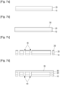
- FIGS. 7a to 7h schematically illustrate different steps of an example of a method according to the invention for manufacturing the electrical circuit 3, this method being implemented continuously.
- a structure comprising a first sheet of electrically conductive material 10 laminated to a substrate of electrically insulating material 20.
- This structure (also called a "clad” in English) can be obtained by directly laminating together the first sheet of electrically conductive material 10 and the substrate of electrically insulating material 20.
- a layer of adhesive material not shown can be coated or laminated onto the first sheet of electrically conductive material 10 and/or the substrate of electrically insulating material 20, before laminating them together with the layer of adhesive material between the two.
- the first sheet of electrically conductive material 10 may be formed from a metal such as copper, steel, aluminum or an alloy of these metals.
- the first sheet of electrically conductive material 10 is for example 18 micrometers or 25 micrometers thick.
- the substrate of electrically insulating material 20 is formed of a dielectric material for example of the composite type (glass-epoxy) or of the plastic type (PET, PEN, polyimide, etc.).
- the substrate of electrically insulating material 20 is generally thin (its thickness is for example of the order of 100 micrometers) to maintain a flexibility compatible with continuous manufacturing processes of electronic modules 3.
- the assembly consisting of the substrate of electrically insulating material 20 covered with the first sheet of electrically conductive material 10 also forms a flexible circuit compatible with continuous manufacturing processes of electronic modules 3.
- a film or layer of adhesive material 30 is applied to the face of the substrate of electrically insulating material 20, opposite that on which the first sheet of electrically conductive material 10 is located.
- holes 40, 40I are punched through the entire structure obtained in the previous step.
- the holes 40, 40I are punched in a direction substantially perpendicular to the plane of this structure.
- a second sheet of electrically conductive material 50 is laminated, on the layer of adhesive material 30, on the face of the substrate of electrically insulating material 20 opposite that on which the first sheet of electrically conductive material 10 is located.
- the bottom of these holes 40, 40I is closed by the second sheet of electrically conductive material 50.
- the holes 40, 40I then become blind holes, also called connection wells (as explained later, these holes 40, 40I are metallized at a later stage to make them electrically conductive).
- the second sheet of electrically conductive material 50 may be formed of a metal such as copper, steel, aluminum or an alloy of these metals.
- the second sheet of electrically conductive material 50 is for example 18, 25 or 35 micrometers thick.
- patterns are produced in a known manner, by photolithography, in each of the first 10 and second 50 sheets of electrically conductive material.
- these patterns comprise contacts 5 and current leads 4 (not visible on the figure 7e ).
- these patterns mainly comprise contact connection pads 51 and antenna 51, as well as an antenna 8.
- one or more layers of electrically conductive materials 60 are deposited electrochemically on at least the contacts 5, on the connection pads 51, 52 and in holes 40. Part of this step (for example the step for making the holes conductive) may have been carried out previously.
- the layer(s) of electrically conductive materials 60 may comprise one or more of the metals included in the following list: nickel, gold, palladium, silver and/or alloys thereof. Masks are optionally used to selectively deposit some of these electrically conductive materials on certain areas and not on others, or in greater or lesser thicknesses depending on the areas and/or the electrically conductive material deposited.
- the electrochemical deposition of this or these layers of electrically conductive materials 60 is important in order to be able to then reliably solder electrically conductive wires 70 electrically connecting the chip 100 to the connection pads 51, 52 onto the connection pads 51, 52.
- the electrochemical deposition of this or these layers of electrically conductive materials 60 onto the rear face 7 is made possible by the passage of current, via the metallized holes 40, 40I, between the current leads 4 and the contacts 5 located on the front face 6 and the connection pads 51, 52, the antenna 8 and any other tracks located on the rear face 7.
- certain contacts 5 are electrically connected to a single metallized hole 40 and essentially to a connection pad 51, while at least one other (on the left on the figure 7f ) is electrically connected to two metallized 40 holes and essentially to a contact connection pad 51 and an antenna connection pad 51.
- the two metallized holes 40 and the two connection pads 51, 52 are therefore short-circuited at least by the front face 6.
- the next step essentially consists of short-circuiting at least some metallized holes 40 and the connection pads 51, 52 electrically connected to each other.
- the insulation is done in particular for the holes that it is essential to isolate.
- This can be done advantageously using a laser beam.
- a circle 90 is made in the layer(s) of electrically conductive materials 60, as well as in the first sheet of electrically conductive material 10. The laser beam thus makes it possible to uncover the substrate of electrically insulating material 20, that is to say to remove at the level of this circle, the layer(s) of electrically conductive materials 60, as well as the first sheet of electrically conductive material 10.
- a closed shape will be preferred which corresponds to a movement of the beam on a material whose structure is homogeneous.
- a movement of the laser beam passing from an area at which the substrate of electrically insulating material 10 is in the bare state, to an area covered with the layer(s) of electrically conductive materials 60, and the first sheet of electrically conductive material 10 requires adjusting the parameters on the laser beam in a suitable manner for each of these areas, which, without being impossible, requires a lot of precision.
- an adjustment of the laser beam is easier to control when it is a question of releasing the substrate of electrically insulating material 20 from a stack of identical layers over the entire path of the laser beam.
- this short-circuiting step illustrated by the Figure 7G can be carried out by photolithography, for example by implementing steps such as the application of a film resistant to electro-deposition ("plating resist" in English), exposure and development of the film, before metallization and etching.
- steps such as the application of a film resistant to electro-deposition ("plating resist" in English), exposure and development of the film, before metallization and etching.
- a chip 100 is attached to the rear face 7 of the electrically insulating material substrate 20. Then conductive wires 70 can be connected to the chip 100, on the one hand, and to the connection pads 51, 52, on the other hand.
- connection wires 70 and the chip 100 in a resin can then be implemented.
- cutting of the electrical circuit 3 to obtain individualized modules 2 can then be implemented.
- the antenna 8 being able to be connected at each of its ends to the front face 6 by a metallized hole 40, a better distribution of the deposition of this or these layers of conductive material 60 is obtained. This makes it possible to reduce the inductance of the antenna 8 and thus improve its radiofrequency performance.
Landscapes
- Engineering & Computer Science (AREA)
- Microelectronics & Electronic Packaging (AREA)
- Computer Hardware Design (AREA)
- Physics & Mathematics (AREA)
- General Physics & Mathematics (AREA)
- Theoretical Computer Science (AREA)
- Computer Networks & Wireless Communication (AREA)
- Credit Cards Or The Like (AREA)
- Details Of Aerials (AREA)
- Printing Elements For Providing Electric Connections Between Printed Circuits (AREA)
Claims (10)
- Verfahren zur elektrochemischen Metallisierung einer doppelseitigen elektrischen Schaltung (3) für eine Chipkarte, die mit und ohne Kontakt kommuniziert, bei dem ein flexibles dielektrisches Substrat (20) mit einer Vorderseite (6) und einer Rückseite (7) bereitgestellt wird, wobei auf der Vorderseite (6) Kontakte (5) und Stromzuführungen (4) vorhanden sind, die mit mindestens einigen der Kontakte (5) elektrisch verbunden sind, und wobei auf der Rückseite (7) eine Antenne (8) und Anschlussflächen (51, 52) vorhanden sind, die für einige (51) gewidmet sind, der Verbindung eines Chips (100) mit den Kontakten (5) und für andere (52) der Verbindung des Chips (100) mit der Antenne (8) dienen, umfasst dieses Verfahren einen Vorgang der elektrochemischen Abscheidung von mindestens einer Schicht aus elektrisch leitendem Material (60) zumindest auf einigen der Anschlussflächen (51, 52), wobei diese Anschlussflächen (51, 52) über die Stromzuführungen (4), Kontakte (5) und metallisierte Löcher (40) mit Strom versorgt werden, die eine elektrische Kontinuität zwischen der Vorderseite (6) und der Rückseite (7) herstellen,
dadurch gekennzeichnet, dass sie nach dem Vorgang der elektrochemischen Abscheidung mindestens einer Schicht aus elektrisch leitfähigem Material (60) einen Vorgang umfasst, der darin besteht, mindestens ein metallisiertes Loch (40I) eines Anschlussflecks (52), der der Verbindung des Chips (100) mit der Antenne (8) gewidmet ist, elektrisch zu isolieren. - Verfahren nach Anspruch 1, bei dem mindestens zwei metallisierte Löcher (40) während des Vorgangs der elektrochemischen Abscheidung mindestens einer Schicht aus elektrisch leitfähigem Material (60) verwendet werden, um einen inneren Antennenanschlussfleck (52) und einen äußeren Antennenanschlussfleck (52) zu metallisieren , wobei mindestens eines dieser beiden metallisierten Löcher (40) in einem Vorgang nach dem elektrochemischen Abscheiden mindestens einer Schicht aus elektrisch leitfähigem Material (60) von den inneren und äußeren Antennenanschlussflächen (52) elektrisch isoliert wird.
- Verfahren nach einem der vorhergehenden Ansprüche, bei dem ein und derselbe Kontakt (5) auf der Vorderseite (6) verwendet wird, der mit zwei getrennten Anschlussflächen (51, 52) verbunden ist, um diese beiden Anschlussflächen (51, 52) während des Vorgangs der elektrochemischen Abscheidung mindestens einer Schicht aus elektrisch leitfähigem Material (60) über zwei metallisierte Löcher (40) mit Strom zu versorgen, wobei mindestens eines dieser beiden metallisierten Löcher (40) anschließend von jeder der Anschlussflächen (51, 52) elektrisch isoliert wird.
- Verfahren nach einem der vorhergehenden Ansprüche, bei dem ein Vorgang der elektrischen Isolierung mindestens eines metallisierten Lochs (40) eines Verbindungsstücks (52), das der Verbindung des Chips (100) mit der Antenne (8) gewidmet ist, mit Hilfe eines Laserstrahls durchgeführt wird.
- Verfahren nach dem vorhergehenden Anspruch, bei dem der Laserstrahl auf der Oberfläche eines leitenden Bereichs bewegt wird, der das metallisierte Loch (40) mit der Anschlussfläche (52) verbindet, die der Verbindung des Chips (100) mit der Antenne (8) gewidmet ist, ohne diese Oberfläche zu verlassen, um das metallisierte Loch (40) herum, um dieses metallisierte Loch (40) vom Rest der Anschlussfläche (52) zu isolieren, die der Verbindung des Chips (100) mit der Antenne (8) gewidmet ist.
- Doppelseitige elektrische Schaltung (3) für eine Chipkarte, die mit und ohne Kontakt kommuniziert, wobei die elektrische Schaltung ein flexibles dielektrisches Substrat (20) mit einer Vorderseite (6) und einer Rückseite (7) umfasst, wobei sich auf der Vorderseite (6) Kontakte (5) und Stromzuführungen (4) befinden, eine Antenne (8) und Anschlussflächen (51, 52), die sich auf der Rückseite (7) befinden, wobei einige (51) der Anschlussflächen der Verbindung eines Chips (100) mit den Kontakten (5) gewidmet sind und andere (52) der Verbindung des Chips (100) mit der Antenne (8) gewidmet sind, dadurch gekennzeichnet, dass er mindestens einen Kontakt (5) umfasst, der mindestens zwei metallisierte Löcher (40) verschließt, wobei eines der metallisierten Löcher (40) mit einem Kontaktanschlussflächen (51) verbunden ist, der der Verbindung des Chips (100) mit diesem Kontakt (5) gewidmet ist, und das andere dieser metallisierten Löcher (40I) elektrisch von einem Antennenanschlussfleck (52) isoliert ist, der der Verbindung des Chips (100) mit der Antenne (8) gewidmet ist.
- Elektrische Schaltung nach dem vorhergehenden Anspruch, bei der ein externes Anschlussfläches (52) der Antenne (8) über zwei metallisierte Löcher (40), die durch eine Leiterbahn (9) verschlossen sind, die sich an der Vorderseite (6) befindet, elektrisch mit der Antenne (8) verbunden ist.
- Elektrische Schaltung nach Anspruch 6, bei der ein externer Anschlussflächer (52) der Antenne (8) über einen Kontakt (5) elektrisch mit der Antenne (8) verbunden ist.
- Elektrische Schaltung nach einem der Ansprüche 6 bis 8, bei der die Antenne (8) mindestens eine Schleife um einen zentralen Bereich bildet, der einem Bereich zur Befestigung des Chips (100) entspricht, und bei der alle Anschlussflächen (51, 52) der Kontakte und der Antenne um diesen zentralen Bereich innerhalb einer Schleife der Antenne angeordnet sind.
- Elektrische Schaltung nach einem der Ansprüche 6 bis 9, wobei mindestens ein metallisiertes Loch (40I), das von allen Anschlussflächen (51, 52) elektrisch isoliert ist, von einem isolierenden Bereich (90) umgeben ist, der durch Abschleifen mit einem Laserstrahl entstanden ist.
Applications Claiming Priority (2)
| Application Number | Priority Date | Filing Date | Title |
|---|---|---|---|
| FR2005425A FR3110735B1 (fr) | 2020-05-21 | 2020-05-21 | Procédé de métallisation électro-chimique d’un circuit électrique double-face pour carte à puce et circuit électrique obtenu par ce procédé. |
| PCT/EP2021/063066 WO2021233869A1 (fr) | 2020-05-21 | 2021-05-18 | Procédé de métallisation électro-chimique d'un circuit électrique double-face pour carte à puce et circuit électrique obtenu par ce procédé. |
Publications (2)
| Publication Number | Publication Date |
|---|---|
| EP4154180A1 EP4154180A1 (de) | 2023-03-29 |
| EP4154180B1 true EP4154180B1 (de) | 2024-08-28 |
Family
ID=72178764
Family Applications (1)
| Application Number | Title | Priority Date | Filing Date |
|---|---|---|---|
| EP21725219.6A Active EP4154180B1 (de) | 2020-05-21 | 2021-05-18 | Verfahren zur elektrochemischen metallisierung einer doppelseitigen elektrischen schaltung für eine chipkarte und mit diesem verfahren hergestellte elektrische schaltung |
Country Status (6)
| Country | Link |
|---|---|
| US (1) | US12106168B2 (de) |
| EP (1) | EP4154180B1 (de) |
| KR (1) | KR20230014742A (de) |
| CN (1) | CN115668213A (de) |
| FR (1) | FR3110735B1 (de) |
| WO (1) | WO2021233869A1 (de) |
Families Citing this family (2)
| Publication number | Priority date | Publication date | Assignee | Title |
|---|---|---|---|---|
| DE102021112447B4 (de) * | 2021-05-12 | 2024-06-20 | Infineon Technologies Ag | Chipkarten-Biometrie-Sensor-Bauteil, Chipkarte, Verfahren zum Bilden eines Chipkarten-Biometrie-Sensor-Bauteils und Verfahren zum Bilden einer Chipkarte |
| KR102744706B1 (ko) * | 2023-02-01 | 2024-12-19 | 주식회사 에이아이엘 | 양방향 비접촉식 결제 기능을 가지는 메탈 소재의 rf 디바이스 |
Family Cites Families (15)
| Publication number | Priority date | Publication date | Assignee | Title |
|---|---|---|---|---|
| TW484101B (en) * | 1998-12-17 | 2002-04-21 | Hitachi Ltd | Semiconductor device and its manufacturing method |
| US7948381B2 (en) * | 2004-04-30 | 2011-05-24 | Binforma Group Limited Liability Company | Reversibly deactivating a radio frequency identification data tag |
| FR2890212B1 (fr) | 2005-08-30 | 2009-08-21 | Smart Packaging Solutions Sps | Module electronique a double interface de communication, notamment pour carte a puce |
| US9272370B2 (en) * | 2010-08-12 | 2016-03-01 | Féinics Amatech Teoranta | Laser ablating structures for antenna modules for dual interface smartcards |
| US8870080B2 (en) * | 2010-08-12 | 2014-10-28 | Féinics Amatech Teoranta | RFID antenna modules and methods |
| FR2994005B1 (fr) * | 2012-07-25 | 2017-05-26 | Microconnections Sas | Module electronique pour carte a puce et circuit imprime pour la realisation d'un tel module |
| FR2997782B1 (fr) * | 2012-11-05 | 2016-01-15 | Linxens Holding | Procede de fabrication d'un connecteur pour module de carte a puce, connecteur de carte a puce obtenu par ce procede et module de carte a puce comportant un tel connecteur. |
| US11354558B2 (en) * | 2013-01-18 | 2022-06-07 | Amatech Group Limited | Contactless smartcards with coupling frames |
| FR3006546B1 (fr) | 2013-05-28 | 2019-03-29 | Sgame | Module de diode electroluminescente lumiere blanche |
| FR3006549B1 (fr) * | 2013-06-03 | 2016-10-14 | Linxens Holding | Procede de realisation d'un circuit electrique et circuit electrique realise par ce procede |
| EP2892012A1 (de) * | 2014-01-06 | 2015-07-08 | Gemalto SA | Elektronisches Modul, sein Herstellungsverfahren und dieses Modul umfassende elektronische Vorrichtung |
| EP3269215B1 (de) * | 2015-03-12 | 2020-04-22 | AT & S Austria Technologie & Systemtechnik Aktiengesellschaft | Leiterplatte und herstellungsverfahren dieser leiterplatte |
| JP6200106B2 (ja) * | 2015-07-08 | 2017-09-20 | コンポーズキュア,リミティド ライアビリティ カンパニー | デュアルインターフェース能力を有する金属スマートカード |
| EP3151167B1 (de) * | 2015-09-30 | 2020-05-20 | Nxp B.V. | Dual-interface ic-kartenmodul |
| US11315003B2 (en) * | 2019-08-14 | 2022-04-26 | Federal Card Services, LLC | RFID enabled metal transaction cards |
-
2020
- 2020-05-21 FR FR2005425A patent/FR3110735B1/fr active Active
-
2021
- 2021-05-18 EP EP21725219.6A patent/EP4154180B1/de active Active
- 2021-05-18 KR KR1020227044913A patent/KR20230014742A/ko active Pending
- 2021-05-18 US US17/926,158 patent/US12106168B2/en active Active
- 2021-05-18 WO PCT/EP2021/063066 patent/WO2021233869A1/fr not_active Ceased
- 2021-05-18 CN CN202180036188.3A patent/CN115668213A/zh active Pending
Also Published As
| Publication number | Publication date |
|---|---|
| CN115668213A (zh) | 2023-01-31 |
| FR3110735B1 (fr) | 2022-04-29 |
| KR20230014742A (ko) | 2023-01-30 |
| EP4154180A1 (de) | 2023-03-29 |
| US12106168B2 (en) | 2024-10-01 |
| FR3110735A1 (fr) | 2021-11-26 |
| WO2021233869A1 (fr) | 2021-11-25 |
| US20230196053A1 (en) | 2023-06-22 |
Similar Documents
| Publication | Publication Date | Title |
|---|---|---|
| EP2877965B1 (de) | Elektronisches modul für eine chipkarte und gedruckte schaltung zur erzeugung eines solchen moduls | |
| EP0671705B1 (de) | Herstellungsverfahren einer Kombi-Karte | |
| EP3437028B1 (de) | Verfahren zur herstellung von chipkarten und von chipkartenantennenträgern | |
| EP3005846B1 (de) | Verfahren zur herstellung einer bestückten schaltung | |
| EP4154180B1 (de) | Verfahren zur elektrochemischen metallisierung einer doppelseitigen elektrischen schaltung für eine chipkarte und mit diesem verfahren hergestellte elektrische schaltung | |
| EP3092604B1 (de) | Elektronisches modul, sein herstellungsverfahren und dieses modul umfassende elektronische vorrichtung | |
| EP3408799B1 (de) | Verfahren zur herstellung eines chipkartenmoduls und chipkarte | |
| WO2015071619A1 (fr) | Procede de fabrication d'un support d'une puce electronique,support de puce et ensemble de tels supports | |
| CA2968070C (fr) | Procede de fabrication d'un module electronique simple face comprenant des zones d'interconnexion | |
| WO2000025265A1 (fr) | Procede de fabrication d'une carte a puce et d'un module electronique destine a etre insere dans une telle carte | |
| EP2866173B1 (de) | Verfahren zur Erzeugung eines elektrischen Schaltkreises, und mit diesem Verfahren erzeugter Schaltkreis | |
| EP2915104B1 (de) | Verfahren zur herstellung einer anschlussvorrichtung für das modul einer smart card, durch das verfahren erhaltene anschlussvorrichtung und modul mit smart card anschlussvorrichtung | |
| WO2002001495A1 (fr) | Carte hybride a ensemble de contact ohmique et puits delocalises | |
| WO2020126573A1 (fr) | Procede de fabrication d'un insert de carte a puce radiofrequence comportant une plaque metallique | |
| WO2017191414A1 (fr) | Procédé de fabrication de cartes à puce et carte à puce obtenue par ce procédé | |
| EP3020068B1 (de) | Elektronisches modul und verfahren zur herstellung davon | |
| EP1201007B1 (de) | Antenne für kontaktlose chipkarte, hybridkarten und elektronische etiketten | |
| EP4571572A1 (de) | Metallchipkarte und verfahren zur herstellung einer metallchipkarte | |
| WO2005064533A1 (fr) | Procedes de fabrication d'une carte du type sans contacts externes, et carte ainsi obtenue | |
| WO2001015504A1 (fr) | Procede de fabrication de cartes a puce hybrides et cartes a puce obtenues par ledit procede | |
| FR3084188A1 (fr) | Carte a puce equipee d'une pluralite d'antennes |
Legal Events
| Date | Code | Title | Description |
|---|---|---|---|
| STAA | Information on the status of an ep patent application or granted ep patent |
Free format text: STATUS: UNKNOWN |
|
| STAA | Information on the status of an ep patent application or granted ep patent |
Free format text: STATUS: THE INTERNATIONAL PUBLICATION HAS BEEN MADE |
|
| PUAI | Public reference made under article 153(3) epc to a published international application that has entered the european phase |
Free format text: ORIGINAL CODE: 0009012 |
|
| STAA | Information on the status of an ep patent application or granted ep patent |
Free format text: STATUS: REQUEST FOR EXAMINATION WAS MADE |
|
| 17P | Request for examination filed |
Effective date: 20221109 |
|
| AK | Designated contracting states |
Kind code of ref document: A1 Designated state(s): AL AT BE BG CH CY CZ DE DK EE ES FI FR GB GR HR HU IE IS IT LI LT LU LV MC MK MT NL NO PL PT RO RS SE SI SK SM TR |
|
| DAV | Request for validation of the european patent (deleted) | ||
| DAX | Request for extension of the european patent (deleted) | ||
| GRAP | Despatch of communication of intention to grant a patent |
Free format text: ORIGINAL CODE: EPIDOSNIGR1 |
|
| STAA | Information on the status of an ep patent application or granted ep patent |
Free format text: STATUS: GRANT OF PATENT IS INTENDED |
|
| INTG | Intention to grant announced |
Effective date: 20240424 |
|
| RIN1 | Information on inventor provided before grant (corrected) |
Inventor name: DUMONT, THIERRY Inventor name: MICHAUDET, NICOLAS |
|
| GRAS | Grant fee paid |
Free format text: ORIGINAL CODE: EPIDOSNIGR3 |
|
| GRAA | (expected) grant |
Free format text: ORIGINAL CODE: 0009210 |
|
| STAA | Information on the status of an ep patent application or granted ep patent |
Free format text: STATUS: THE PATENT HAS BEEN GRANTED |
|
| AK | Designated contracting states |
Kind code of ref document: B1 Designated state(s): AL AT BE BG CH CY CZ DE DK EE ES FI FR GB GR HR HU IE IS IT LI LT LU LV MC MK MT NL NO PL PT RO RS SE SI SK SM TR |
|
| REG | Reference to a national code |
Ref country code: CH Ref legal event code: EP |
|
| REG | Reference to a national code |
Ref country code: DE Ref legal event code: R096 Ref document number: 602021017934 Country of ref document: DE |
|
| REG | Reference to a national code |
Ref country code: IE Ref legal event code: FG4D Free format text: LANGUAGE OF EP DOCUMENT: FRENCH |
|
| REG | Reference to a national code |
Ref country code: NL Ref legal event code: FP |
|
| REG | Reference to a national code |
Ref country code: LT Ref legal event code: MG9D |
|
| PG25 | Lapsed in a contracting state [announced via postgrant information from national office to epo] |
Ref country code: NO Free format text: LAPSE BECAUSE OF FAILURE TO SUBMIT A TRANSLATION OF THE DESCRIPTION OR TO PAY THE FEE WITHIN THE PRESCRIBED TIME-LIMIT Effective date: 20241128 |
|
| REG | Reference to a national code |
Ref country code: AT Ref legal event code: MK05 Ref document number: 1718774 Country of ref document: AT Kind code of ref document: T Effective date: 20240828 |
|
| PG25 | Lapsed in a contracting state [announced via postgrant information from national office to epo] |
Ref country code: PL Free format text: LAPSE BECAUSE OF FAILURE TO SUBMIT A TRANSLATION OF THE DESCRIPTION OR TO PAY THE FEE WITHIN THE PRESCRIBED TIME-LIMIT Effective date: 20240828 Ref country code: GR Free format text: LAPSE BECAUSE OF FAILURE TO SUBMIT A TRANSLATION OF THE DESCRIPTION OR TO PAY THE FEE WITHIN THE PRESCRIBED TIME-LIMIT Effective date: 20241129 Ref country code: FI Free format text: LAPSE BECAUSE OF FAILURE TO SUBMIT A TRANSLATION OF THE DESCRIPTION OR TO PAY THE FEE WITHIN THE PRESCRIBED TIME-LIMIT Effective date: 20240828 Ref country code: PT Free format text: LAPSE BECAUSE OF FAILURE TO SUBMIT A TRANSLATION OF THE DESCRIPTION OR TO PAY THE FEE WITHIN THE PRESCRIBED TIME-LIMIT Effective date: 20241230 |
|
| PG25 | Lapsed in a contracting state [announced via postgrant information from national office to epo] |
Ref country code: BG Free format text: LAPSE BECAUSE OF FAILURE TO SUBMIT A TRANSLATION OF THE DESCRIPTION OR TO PAY THE FEE WITHIN THE PRESCRIBED TIME-LIMIT Effective date: 20240828 |
|
| PG25 | Lapsed in a contracting state [announced via postgrant information from national office to epo] |
Ref country code: LV Free format text: LAPSE BECAUSE OF FAILURE TO SUBMIT A TRANSLATION OF THE DESCRIPTION OR TO PAY THE FEE WITHIN THE PRESCRIBED TIME-LIMIT Effective date: 20240828 |
|
| PG25 | Lapsed in a contracting state [announced via postgrant information from national office to epo] |
Ref country code: IS Free format text: LAPSE BECAUSE OF FAILURE TO SUBMIT A TRANSLATION OF THE DESCRIPTION OR TO PAY THE FEE WITHIN THE PRESCRIBED TIME-LIMIT Effective date: 20241228 Ref country code: AT Free format text: LAPSE BECAUSE OF FAILURE TO SUBMIT A TRANSLATION OF THE DESCRIPTION OR TO PAY THE FEE WITHIN THE PRESCRIBED TIME-LIMIT Effective date: 20240828 |
|
| PG25 | Lapsed in a contracting state [announced via postgrant information from national office to epo] |
Ref country code: HR Free format text: LAPSE BECAUSE OF FAILURE TO SUBMIT A TRANSLATION OF THE DESCRIPTION OR TO PAY THE FEE WITHIN THE PRESCRIBED TIME-LIMIT Effective date: 20240828 |
|
| PG25 | Lapsed in a contracting state [announced via postgrant information from national office to epo] |
Ref country code: RS Free format text: LAPSE BECAUSE OF FAILURE TO SUBMIT A TRANSLATION OF THE DESCRIPTION OR TO PAY THE FEE WITHIN THE PRESCRIBED TIME-LIMIT Effective date: 20241128 Ref country code: ES Free format text: LAPSE BECAUSE OF FAILURE TO SUBMIT A TRANSLATION OF THE DESCRIPTION OR TO PAY THE FEE WITHIN THE PRESCRIBED TIME-LIMIT Effective date: 20240828 |
|
| PG25 | Lapsed in a contracting state [announced via postgrant information from national office to epo] |
Ref country code: RS Free format text: LAPSE BECAUSE OF FAILURE TO SUBMIT A TRANSLATION OF THE DESCRIPTION OR TO PAY THE FEE WITHIN THE PRESCRIBED TIME-LIMIT Effective date: 20241128 Ref country code: PT Free format text: LAPSE BECAUSE OF FAILURE TO SUBMIT A TRANSLATION OF THE DESCRIPTION OR TO PAY THE FEE WITHIN THE PRESCRIBED TIME-LIMIT Effective date: 20241230 Ref country code: PL Free format text: LAPSE BECAUSE OF FAILURE TO SUBMIT A TRANSLATION OF THE DESCRIPTION OR TO PAY THE FEE WITHIN THE PRESCRIBED TIME-LIMIT Effective date: 20240828 Ref country code: NO Free format text: LAPSE BECAUSE OF FAILURE TO SUBMIT A TRANSLATION OF THE DESCRIPTION OR TO PAY THE FEE WITHIN THE PRESCRIBED TIME-LIMIT Effective date: 20241128 Ref country code: LV Free format text: LAPSE BECAUSE OF FAILURE TO SUBMIT A TRANSLATION OF THE DESCRIPTION OR TO PAY THE FEE WITHIN THE PRESCRIBED TIME-LIMIT Effective date: 20240828 Ref country code: IS Free format text: LAPSE BECAUSE OF FAILURE TO SUBMIT A TRANSLATION OF THE DESCRIPTION OR TO PAY THE FEE WITHIN THE PRESCRIBED TIME-LIMIT Effective date: 20241228 Ref country code: HR Free format text: LAPSE BECAUSE OF FAILURE TO SUBMIT A TRANSLATION OF THE DESCRIPTION OR TO PAY THE FEE WITHIN THE PRESCRIBED TIME-LIMIT Effective date: 20240828 Ref country code: GR Free format text: LAPSE BECAUSE OF FAILURE TO SUBMIT A TRANSLATION OF THE DESCRIPTION OR TO PAY THE FEE WITHIN THE PRESCRIBED TIME-LIMIT Effective date: 20241129 Ref country code: FI Free format text: LAPSE BECAUSE OF FAILURE TO SUBMIT A TRANSLATION OF THE DESCRIPTION OR TO PAY THE FEE WITHIN THE PRESCRIBED TIME-LIMIT Effective date: 20240828 Ref country code: ES Free format text: LAPSE BECAUSE OF FAILURE TO SUBMIT A TRANSLATION OF THE DESCRIPTION OR TO PAY THE FEE WITHIN THE PRESCRIBED TIME-LIMIT Effective date: 20240828 Ref country code: BG Free format text: LAPSE BECAUSE OF FAILURE TO SUBMIT A TRANSLATION OF THE DESCRIPTION OR TO PAY THE FEE WITHIN THE PRESCRIBED TIME-LIMIT Effective date: 20240828 Ref country code: AT Free format text: LAPSE BECAUSE OF FAILURE TO SUBMIT A TRANSLATION OF THE DESCRIPTION OR TO PAY THE FEE WITHIN THE PRESCRIBED TIME-LIMIT Effective date: 20240828 |
|
| PG25 | Lapsed in a contracting state [announced via postgrant information from national office to epo] |
Ref country code: DK Free format text: LAPSE BECAUSE OF FAILURE TO SUBMIT A TRANSLATION OF THE DESCRIPTION OR TO PAY THE FEE WITHIN THE PRESCRIBED TIME-LIMIT Effective date: 20240828 Ref country code: SM Free format text: LAPSE BECAUSE OF FAILURE TO SUBMIT A TRANSLATION OF THE DESCRIPTION OR TO PAY THE FEE WITHIN THE PRESCRIBED TIME-LIMIT Effective date: 20240828 Ref country code: RO Free format text: LAPSE BECAUSE OF FAILURE TO SUBMIT A TRANSLATION OF THE DESCRIPTION OR TO PAY THE FEE WITHIN THE PRESCRIBED TIME-LIMIT Effective date: 20240828 |
|
| PG25 | Lapsed in a contracting state [announced via postgrant information from national office to epo] |
Ref country code: EE Free format text: LAPSE BECAUSE OF FAILURE TO SUBMIT A TRANSLATION OF THE DESCRIPTION OR TO PAY THE FEE WITHIN THE PRESCRIBED TIME-LIMIT Effective date: 20240828 |
|
| PG25 | Lapsed in a contracting state [announced via postgrant information from national office to epo] |
Ref country code: CZ Free format text: LAPSE BECAUSE OF FAILURE TO SUBMIT A TRANSLATION OF THE DESCRIPTION OR TO PAY THE FEE WITHIN THE PRESCRIBED TIME-LIMIT Effective date: 20240828 |
|
| PG25 | Lapsed in a contracting state [announced via postgrant information from national office to epo] |
Ref country code: SK Free format text: LAPSE BECAUSE OF FAILURE TO SUBMIT A TRANSLATION OF THE DESCRIPTION OR TO PAY THE FEE WITHIN THE PRESCRIBED TIME-LIMIT Effective date: 20240828 Ref country code: IT Free format text: LAPSE BECAUSE OF FAILURE TO SUBMIT A TRANSLATION OF THE DESCRIPTION OR TO PAY THE FEE WITHIN THE PRESCRIBED TIME-LIMIT Effective date: 20240828 |
|
| REG | Reference to a national code |
Ref country code: DE Ref legal event code: R097 Ref document number: 602021017934 Country of ref document: DE |
|
| PGFP | Annual fee paid to national office [announced via postgrant information from national office to epo] |
Ref country code: NL Payment date: 20250522 Year of fee payment: 5 |
|
| PLBE | No opposition filed within time limit |
Free format text: ORIGINAL CODE: 0009261 |
|
| STAA | Information on the status of an ep patent application or granted ep patent |
Free format text: STATUS: NO OPPOSITION FILED WITHIN TIME LIMIT |
|
| PGFP | Annual fee paid to national office [announced via postgrant information from national office to epo] |
Ref country code: DE Payment date: 20250519 Year of fee payment: 5 |
|
| PGFP | Annual fee paid to national office [announced via postgrant information from national office to epo] |
Ref country code: GB Payment date: 20250522 Year of fee payment: 5 |
|
| PGFP | Annual fee paid to national office [announced via postgrant information from national office to epo] |
Ref country code: FR Payment date: 20250523 Year of fee payment: 5 |
|
| 26N | No opposition filed |
Effective date: 20250530 |
|
| PG25 | Lapsed in a contracting state [announced via postgrant information from national office to epo] |
Ref country code: SE Free format text: LAPSE BECAUSE OF FAILURE TO SUBMIT A TRANSLATION OF THE DESCRIPTION OR TO PAY THE FEE WITHIN THE PRESCRIBED TIME-LIMIT Effective date: 20240828 |
|
| REG | Reference to a national code |
Ref country code: CH Ref legal event code: H13 Free format text: ST27 STATUS EVENT CODE: U-0-0-H10-H13 (AS PROVIDED BY THE NATIONAL OFFICE) Effective date: 20251223 |
|
| PG25 | Lapsed in a contracting state [announced via postgrant information from national office to epo] |
Ref country code: LU Free format text: LAPSE BECAUSE OF NON-PAYMENT OF DUE FEES Effective date: 20250518 |
|
| PG25 | Lapsed in a contracting state [announced via postgrant information from national office to epo] |
Ref country code: CH Free format text: LAPSE BECAUSE OF NON-PAYMENT OF DUE FEES Effective date: 20250531 |
|
| REG | Reference to a national code |
Ref country code: BE Ref legal event code: MM Effective date: 20250531 |
|
| PG25 | Lapsed in a contracting state [announced via postgrant information from national office to epo] |
Ref country code: MC Free format text: LAPSE BECAUSE OF FAILURE TO SUBMIT A TRANSLATION OF THE DESCRIPTION OR TO PAY THE FEE WITHIN THE PRESCRIBED TIME-LIMIT Effective date: 20240828 |
|
| PG25 | Lapsed in a contracting state [announced via postgrant information from national office to epo] |
Ref country code: IE Free format text: LAPSE BECAUSE OF NON-PAYMENT OF DUE FEES Effective date: 20250518 |
|
| PG25 | Lapsed in a contracting state [announced via postgrant information from national office to epo] |
Ref country code: BE Free format text: LAPSE BECAUSE OF NON-PAYMENT OF DUE FEES Effective date: 20250531 |