EP4152913A1 - Lichtemittierende vorrichtung und elektronische vorrichtung damit - Google Patents
Lichtemittierende vorrichtung und elektronische vorrichtung damit Download PDFInfo
- Publication number
- EP4152913A1 EP4152913A1 EP22195349.0A EP22195349A EP4152913A1 EP 4152913 A1 EP4152913 A1 EP 4152913A1 EP 22195349 A EP22195349 A EP 22195349A EP 4152913 A1 EP4152913 A1 EP 4152913A1
- Authority
- EP
- European Patent Office
- Prior art keywords
- group
- compound
- light
- emitting device
- blue
- Prior art date
- Legal status (The legal status is an assumption and is not a legal conclusion. Google has not performed a legal analysis and makes no representation as to the accuracy of the status listed.)
- Pending
Links
Images














Classifications
-
- H—ELECTRICITY
- H10—SEMICONDUCTOR DEVICES; ELECTRIC SOLID-STATE DEVICES NOT OTHERWISE PROVIDED FOR
- H10K—ORGANIC ELECTRIC SOLID-STATE DEVICES
- H10K59/00—Integrated devices, or assemblies of multiple devices, comprising at least one organic light-emitting element covered by group H10K50/00
- H10K59/30—Devices specially adapted for multicolour light emission
- H10K59/32—Stacked devices having two or more layers, each emitting at different wavelengths
-
- H—ELECTRICITY
- H10—SEMICONDUCTOR DEVICES; ELECTRIC SOLID-STATE DEVICES NOT OTHERWISE PROVIDED FOR
- H10K—ORGANIC ELECTRIC SOLID-STATE DEVICES
- H10K50/00—Organic light-emitting devices
- H10K50/10—OLEDs or polymer light-emitting diodes [PLED]
- H10K50/11—OLEDs or polymer light-emitting diodes [PLED] characterised by the electroluminescent [EL] layers
- H10K50/12—OLEDs or polymer light-emitting diodes [PLED] characterised by the electroluminescent [EL] layers comprising dopants
- H10K50/121—OLEDs or polymer light-emitting diodes [PLED] characterised by the electroluminescent [EL] layers comprising dopants for assisting energy transfer, e.g. sensitization
-
- H—ELECTRICITY
- H10—SEMICONDUCTOR DEVICES; ELECTRIC SOLID-STATE DEVICES NOT OTHERWISE PROVIDED FOR
- H10K—ORGANIC ELECTRIC SOLID-STATE DEVICES
- H10K50/00—Organic light-emitting devices
- H10K50/10—OLEDs or polymer light-emitting diodes [PLED]
- H10K50/11—OLEDs or polymer light-emitting diodes [PLED] characterised by the electroluminescent [EL] layers
- H10K50/125—OLEDs or polymer light-emitting diodes [PLED] characterised by the electroluminescent [EL] layers specially adapted for multicolour light emission, e.g. for emitting white light
- H10K50/13—OLEDs or polymer light-emitting diodes [PLED] characterised by the electroluminescent [EL] layers specially adapted for multicolour light emission, e.g. for emitting white light comprising stacked EL layers within one EL unit
-
- H—ELECTRICITY
- H10—SEMICONDUCTOR DEVICES; ELECTRIC SOLID-STATE DEVICES NOT OTHERWISE PROVIDED FOR
- H10K—ORGANIC ELECTRIC SOLID-STATE DEVICES
- H10K50/00—Organic light-emitting devices
- H10K50/10—OLEDs or polymer light-emitting diodes [PLED]
- H10K50/19—Tandem OLEDs
-
- H—ELECTRICITY
- H10—SEMICONDUCTOR DEVICES; ELECTRIC SOLID-STATE DEVICES NOT OTHERWISE PROVIDED FOR
- H10K—ORGANIC ELECTRIC SOLID-STATE DEVICES
- H10K59/00—Integrated devices, or assemblies of multiple devices, comprising at least one organic light-emitting element covered by group H10K50/00
- H10K59/30—Devices specially adapted for multicolour light emission
- H10K59/38—Devices specially adapted for multicolour light emission comprising colour filters or colour changing media [CCM]
-
- H—ELECTRICITY
- H10—SEMICONDUCTOR DEVICES; ELECTRIC SOLID-STATE DEVICES NOT OTHERWISE PROVIDED FOR
- H10K—ORGANIC ELECTRIC SOLID-STATE DEVICES
- H10K85/00—Organic materials used in the body or electrodes of devices covered by this subclass
- H10K85/30—Coordination compounds
- H10K85/341—Transition metal complexes, e.g. Ru(II)polypyridine complexes
- H10K85/342—Transition metal complexes, e.g. Ru(II)polypyridine complexes comprising iridium
-
- H—ELECTRICITY
- H10—SEMICONDUCTOR DEVICES; ELECTRIC SOLID-STATE DEVICES NOT OTHERWISE PROVIDED FOR
- H10K—ORGANIC ELECTRIC SOLID-STATE DEVICES
- H10K85/00—Organic materials used in the body or electrodes of devices covered by this subclass
- H10K85/30—Coordination compounds
- H10K85/341—Transition metal complexes, e.g. Ru(II)polypyridine complexes
- H10K85/346—Transition metal complexes, e.g. Ru(II)polypyridine complexes comprising platinum
Definitions
- the present disclosure relates to light-emitting devices and electronic apparatuses including the same.
- OLEDs organic light-emitting devices
- OLEDs are self-emission devices, which have improved characteristics in terms of viewing angles, response time, luminance, driving voltage, and response speed, and produce full-color images.
- an organic light-emitting device includes an anode, a cathode, and an organic layer located between the anode and the cathode, wherein the organic layer includes an emission layer.
- a hole transport region may be located between the anode and the emission layer, and an electron transport region may be located between the emission layer and the cathode.
- Holes provided from the anode may move toward the emission layer through the hole transport region, and electrons provided from the cathode may move toward the emission layer through the electron transport region.
- the holes and the electrons recombine in the emission layer to produce excitons. These excitons transition from an excited state to a ground state to thereby generate light.
- a light-emitting device including a plurality of color conversion elements uses a blue-organic light-emitting device substrate or a white-organic light-emitting device substrate as a light source.
- light-emitting devices having high luminescence efficiency and long lifespans, and electronic apparatuses including the same.
- a light-emitting device includes:
- Both the first compound and the second compound may emit a green light.
- a light-emitting device includes:
- an organic light-emitting device (OLED) substrate including a structure in which at least one blue emission unit and at least one green emission unit are stacked, wherein the OLED substrate emits blue light and green light,
- Both the first compound and the second compound may emit a green light.
- an organic light-emitting device (OLED) substrate including a structure in which at least one blue emission unit and at least one green emission unit are stacked, wherein the OLED substrate emits blue light and green light,
- an electronic apparatus includes the light-emitting device.
- first, second, third etc. may be used herein to describe various elements, components, regions, layers, and/or sections, these elements, components, regions, layers, and/or sections should not be limited by these terms. These terms are only used to distinguish one element, component, region, layer, or section from another element, component, region, layer, or section. Thus, a first element, component, region, layer, or section discussed below could be termed a second element, component, region, layer, or section without departing from the teachings of the present embodiments.
- Exemplary embodiments are described herein with reference to cross section illustrations that are schematic illustrations of idealized embodiments. As such, variations from the shapes of the illustrations as a result, for example, of manufacturing techniques and/or tolerances, are to be expected. Thus, embodiments described herein should not be construed as limited to the particular shapes of regions as illustrated herein but are to include deviations in shapes that result, for example, from manufacturing. For example, a region illustrated or described as flat may, typically, have rough and/or nonlinear features. Moreover, sharp angles that are illustrated may be rounded. Thus, the regions illustrated in the figures are schematic in nature and their shapes are not intended to illustrate the precise shape of a region and are not intended to limit the scope of the present claims.
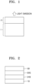
- FIG. 1 is a cross-sectional view illustrating a light-emitting device according to one or more embodiments.
- the light-emitting device of FIG. 1 may include an organic light-emitting device (OLED) substrate 1 and a color control unit 2 located in a path of light emitted from the OLED substrate 1 to control the color of light generated from the OLED substrate 1.
- OLED substrate 1 may act as a light source.
- the number of emission units included in the OLED substrate 1 may be two or more, or for example, 2 to 20, or 2 to 10. In one or more embodiments, the number of emission units included in the OLED substrate 1 may be 2, 3, 4, or 5.
- the OLED substrate 1 includes a structure in which at least one blue emission unit and at least one green emission unit are stacked, for example sequentially stacked.
- the at least one blue emission unit and the at least one green emission unit may be connected in series to each other to form a tandem structure. Accordingly, the OLED substrate 1 may have a tandem structure.
- Each of the blue emission units may emit a blue light having an emission peak wavelength of about 440 nanometers (nm) to about 500 nm, or about 450 nm to about 480 nm.
- Each of the green emission units may emit a green light having an emission peak wavelength of about 500 nm to about 570 nm, or about 510 nm to about 550 nm.
- the number of the blue emission units included in the OLED substrate 1 may be the same as or greater than the number of the green emission units. In one or more embodiments, the ratio of the number of the blue emission units to the number of the green emission units may be 1:1 to 10:1, or 1:1 to 5:1.
- the number of the blue emission units may be 1, 2, 3, 4, or 5 and the number of the green emission units may be 1, 2, 3, or 4.
- the number of the blue emission units may be 1, 2, or 3, and the number of the green emission units may be 1 or 2.
- the number of the blue emission units may be 2 or 3, and the number of the green emission units may be 1 or 2. In one or more embodiments, the number of the blue emission units may 3, and the number of the green emission units may be 1.
- the stacking order of the at least one blue emission unit and the at least one green emission unit may be variously modified.
- the at least one blue emission unit and the at least one green emission unit may be alternately stacked.
- the at least one green emission unit (for example, all green emission units) may be located closer to the color control unit 2 than the at least one blue emission unit (for example, all blue emission units).
- mixed light including blue light and green light is emitted.
- the at least one green emission units of the OLED substrate 1 includes a first compound and a second compound, for example, the first compound and the second compound may be mixed.
- the first compound and the second compound are different from each other.
- the at least one green emission units of the OLED substrate 1 may include a layer including a mixture of the first compound and the second compound.
- the layer including the mixture of the first compound and the second compound may be formed by i) a co-deposition process or ii) a soluble process including providing a first solution and a heat treatment.
- a deposition target material may include a first compound and a second compound
- the first solution may include the first compound and the second compound. Therefore, the "layer including the mixture of the first compound and the second compound" is clearly distinguished from, for example, a double-layer structure in which a layer containing the first compound and a layer containing the second compound are stacked.
- the color control unit 2 may include a quantum dot, an inorganic phosphor, an organic fluorescent material, an organic phosphorescent material, or a combination thereof. In one or more embodiments, the color control unit 2 may include a plurality of quantum dots.
- the color control unit 2 may include a first color control element for green conversion and a second color control element for red conversion.
- the first color control element and the second color control element may be patterned for corresponding pixels capable of emitting a different color of light.
- the color control unit 2 may include a first color control element for green conversion, a second color control element for red conversion, and a third color control element for blue conversion.
- the first color control element, the second color control element, and the third color control element may be patterned for corresponding pixels capable of emitting a different color of light.
- each of the first color control element and the second color control element may be a color conversion element.
- each of the first color control element and the second color control element may be a quantum dot-containing color conversion element.
- the third color control element may be a color conversion element or a color filter.
- the third color control element may be a quantum dot-containing color conversion element or an absorption type color filter.
- the color control unit 2 may include a first color control element including a first quantum dot for green conversion, a second color control element including a second quantum dot for red conversion, and a third color control element for blue conversion.
- the color control unit 2 may further include a first color filter located on the first color control element, and a second color filter located on the second color control element.
- the light-emitting device may further include a thin-film transistor (TFT) array substrate including a plurality of TFTs (not shown).
- the plurality of TFTs of the TFT array substrate may be a device for driving pixel (subpixel) regions of the OLED substrate 1.
- the TFT array substrate may be located under or below the OLED substrate 1.
- the TFT array substrate may be located between the OLED substrate 1 and the color control unit 2.
- Located between the OLED substrate 1 and the color control unit 2 may be an optical film (for example, a selective reflection film, a capping layer, or the like) that may control the optical characteristics of the light-emitting device in various ways; an encapsulating member to prevent oxygen and/or moisture from external air from reaching the OLED substrate 1; or the like.
- an optical film for example, a selective reflection film, a capping layer, or the like
- an encapsulating member to prevent oxygen and/or moisture from external air from reaching the OLED substrate 1; or the like.
- a selective reflection film may be additionally located between the OLED substrate 1 and the color control unit 2.
- the selective reflection film may be configured to transmit blue light and green light and to reflect red light.
- the selective reflection film may act to transmit a wavelength band of about 440 nm to about 550 nm and reflect a wavelength band of about 610 nm to about 760 nm. Accordingly, the mixed light including blue light and green light emitted from the OLED substrate 1 may be irradiated to the color control unit 2 through the selective reflection film.
- red light emitted downward from the second color control element 70b which will be described later, may be reflected by the selective reflection film and emitted upward. Accordingly, the optical efficiency may be improved by the selective reflection film.
- the selective reflection film may be optionally formed only under the second color control element 70b, which will be described later.
- the selective reflection film may be formed in a distributed Bragg reflector (DBR) structure.
- DBR distributed Bragg reflector
- a DBR structure that passes or reflects only the desired wavelength band may be created by repeatedly stacking two material layers (dielectrics) having different refractive indices and adjusting the thickness and the number of layers to be stacked of the material layers.
- the DBR structure may be applied to the selective reflection film.
- a first dielectric layer and a second dielectric layer may be repeatedly stacked, and the reflectance or transmittance of the desired wavelength band may be increased by adjusting the material, the thickness, and the number of layers to be stacked of the material layers.
- the selective reflection film may have a dichroic mirror structure.
- the light-emitting device may not emit white light.
- the first compound emits first light having a first spectrum and AP(1) is a first emission peak wavelength (nm) of the first spectrum
- the second compound emits second light having a second spectrum and ⁇ P(2) is a second emission peak wavelength (nm) in the second spectrum.
- the absolute value of the difference between the ⁇ P(1) and ⁇ P(2) is from 0 nm to about 30 nm, 0 nm to about 25 nm, 0 nm to about 20 nm, 0 nm to about 15 nm, or 0 nm to about 10 nm
- ⁇ P(1) and ⁇ P(2) are each independently about 500 nm to about 570 nm, or about 500 nm to about 550 nm.
- each of ⁇ P(1) and AP(2) may independently be about 500 nm to about 540 nm, or about 510 nm to about 540 nm.
- ⁇ P(1) and AP(2) are evaluated from the photoluminescence (PL) spectra measured with respect to the first film and the second film, respectively, and are emission peak wavelengths in the corresponding photoluminescence spectra, respectively.
- ⁇ P(1) is evaluated from a first photoluminescence spectrum measured from a first film comprising the first compound and is an emission peak wavelengths in the first photoluminescence spectrum
- ⁇ P(2) is evaluated from a second photoluminescence spectrum measured from a second film comprising the second compound and is an emission peak wavelengths in the second photoluminescence spectrum.
- first film refers to a film including the first compound
- second film refers to a film including the second compound.
- the first film and the second film may be manufactured using various methods, for example, a vacuum deposition method, and a coating and heating method.
- the first film and the second film may further include a compound, for example, a host described herein, other than the first compound and the second compound.
- the first compound and the second compound may each be an emitter.
- both the first compound and the second compound may emit a green light.
- the first compound and the second compound may each be an emitter, and AP(1) and ⁇ P(2) may each independently be about 510 nm to about 540 nm.
- the first compound may be a sensitizer
- the second compound may be an emitter
- the first compound may be a sensitizer
- the second compound may be an emitter
- ⁇ P(1) may be about 500 nm to about 520 nm
- AP(2) may be about 510 nm to about 540 nm.
- the first compound and the second compound may each be a phosphorescent compound.
- the phosphorescent compound may be an organometallic compound containing a transition metal (for example, iridium, platinum, osmium, or the like), and may be electrically neutral.
- a transition metal for example, iridium, platinum, osmium, or the like
- the phosphorescent compound may be a platinum-containing organometallic compound or an iridium-containing organometallic compound.
- the platinum-containing organometallic compound may be a platinum-containing organometallic compound including platinum and a tetradentate ligand bonded to the platinum.
- the tetradentate ligand includes a carbon atom and an oxygen atom (or, a sulfur atom) of the tetradentate ligand
- the platinum-containing organometallic compound may include a chemical bond between the carbon atom of the tetradentate ligand and the platinum, and a chemical bond between the oxygen atom (or, the sulfur atom) and the platinum.
- the first compound may be a phosphorescent compound
- the second compound may be a fluorescent compound
- the first compound and the second compound may each independently be a fluorescent compound.
- the fluorescent compound may be a thermally-activated delayed fluorescence (TADF) compound, or a prompt fluorescent compound.
- TADF thermally-activated delayed fluorescence
- each of the first compound and the second compound may independently be a fluorescent compound, wherein the first compound may be a thermally-activated delayed fluorescence compound, and the second compound may be a prompt fluorescent compound.
- the first compound and the second compound may satisfy Condition 1 or Condition 2:
- the first compound is a platinum-containing organometallic compound including platinum and a tetradentate ligand bonded to the platinum, and the second compound is an iridium-containing organometallic compound.
- Each of the first compound and the second compound is independently an iridium-containing organometallic compound.
- the first compound and the second compound may satisfy Condition 1
- aggregation among molecules of the first compound in the mixture, aggregation among molecules of the second compound in the mixture, and/or aggregation among molecules of the first compound and molecules of the second compound in the mixture may be substantially minimized. Accordingly, without any consideration about intermolecular aggregation, the amounts (for example, weight) of the first compound and the second compound in the mixture may be relatively increased. Accordingly, a layer including the mixture and a light-emitting device including the mixture may have excellent luminescence efficiency and lifespan characteristics.
- an emission unit of a light-emitting device contains a mixture of the first compound and the second compound which satisfy Condition 1
- the hole flux in the emission unit is increased due to the mixture, so that an exciton recombination zone in the emission unit may be spaced apart from each of the interface between an emission layer and a hole transport region and the interface between an emission layer and an electron transport region, resulting in improved lifespan characteristics of the light-emitting device.
- the platinum-containing organometallic compound includes one platinum atom and may contain no metal(s) other than platinum.
- the platinum-containing organometallic compound may contain no ligands other than the tetradentate ligand bound to the platinum.
- the tetradentate ligand bound to platinum in the platinum-containing organometallic compounds may have excellent electrical characteristics and structural rigidity.
- the platinum-containing organometallic compound having the tetradentate ligand bound to platinum has a planar structure and may have a relatively small dipole moment.
- the layer including the platinum-containing organometallic compound or the light-emitting device including the platinum-containing organometallic compound have excellent luminescence efficiency and a long lifespan.
- the iridium-containing organometallic compound contains one iridium atom and may contain no metal(s) other than iridium.
- the terms “electric dipole moment of the first compound” and “electric dipole moment of the second compound” as used herein may refer to “total permanent dipole moment in the molecule of the first compound” and “total permanent dipole moment in the molecule of the second compound”, respectively.
- ⁇ (Pt) may be from about 0.5 debye to about 5.0 debye.
- ⁇ (Pt) may be from about 0.5 debye to about 3.0 debye, about 1.0 debye to about 3.0 debye, about 1.5 debye to about 3.0 debye, about 1.7 debye to about 3.0 debye, or about 1.7 debye to about 2.7 debye.
- ⁇ (Pt) may be from about 2.0 debye to about 5.0 debye, about 3.0 debye to about 5.0 debye, or about 4.0 debye to about 5.0 debye.
- ⁇ (Ir) may be from about 4.0 debye to about 9.0 debye, about 4.5 debye to about 7.5 debye, or about 5.0 debye to about 7.0 debye.
- ⁇ (Ir) - ⁇ (Pt) may be from about 0.3 debye to about 4.0 debye.
- ⁇ (Ir) - ⁇ (Pt) may be from about 2.0 debye to about 4.0 debye or about 2.0 debye to about 3.0 debye.
- ⁇ (Ir) - ⁇ (Pt) may be from about 0.3 debye to about 1.0 debye.
- the light emitting device may satisfy Condition 2, and at least one of Equation 1 to Equation 4. Accordingly, a light-emitting device including the first compound and the second compound satisfies Condition 2 may have better luminescence efficiency and long lifespan: ⁇ P Ir 1 > ⁇ P Ir 2 PLQY Ir 1 > PLYQ Ir 2 k r Ir 1 > k r Ir 2 HOR Ir 1 > HOR Ir 2 wherein, in Equation 1, ⁇ P(Ir1) is the first emission peak wavelength ⁇ P(1) of the first compound, as evaluated from the first photoluminescence spectrum measured from the first film comprising the first compound, and ⁇ P(Ir2) is the second emission peak wavelength ⁇ P(2) of the second compound, as evaluated from the second photoluminescence spectrum measured from the second film comprising the second compound,.
- PLQY(Ir1) is the first photoluminescence (PL) quantum yield of the first compound, as evaluated from the first PL spectrum measured from the first film comprising the first compound
- PLQY(Ir2) is the second PL quantum yield of the second compound, as evaluated from the second PL spectrum measured from the second film comprising the second compound.
- kr(Ir1) is a first radiative decay rate of the first compound, as evaluated from the first PL spectrum and first time-resolved PL spectra measured from the first film comprising the first compound
- kr(lr2) is a second radiative decay rate of the second compound, as evaluated from the second PL spectrum and second time-resolved PL spectra measured from the second film comprising the second compound.
- HOR(Ir1) is a first horizontal orientation ratio of the first compound, as evaluated from a first emission intensity with respect to a first angle measured from the first film comprising the first compound
- HOR(Ir2) is a second horizontal orientation ratio of the second compound, as evaluated from a second emission intensity with respect to a second angle measured from the second film comprising the second compound.
- the first film and the second film are those described in the present specification.
- the light-emitting device including the first compound and the second compound that satisfies Condition 2 may satisfy:
- the light-emitting device including the first compound and the second compound that satisfy Condition 2 may further satisfy Equation 5: HOMO Ir 1 ⁇ HOMO Ir 2 wherein, in Equation 5,
- Each of HOMO (Ir1) and HOMO (Ir2) may be a negative value measured using an atmospheric photoelectron spectrometer, for example, AC3 manufactured by RIKEN KEIKI Co., Ltd.
- the second compound in the mixture has a shallower HOMO energy level than the first compound, and a relatively greater amount of holes may be trapped in the second compound.
- the light-emitting device including the mixture without the phenomenon in which the first compound and the second compound are changed into an anionic state due to electrons injected into the mixture and the increase in the driving voltage, holes and electrons may effectively recombine in the first compound and/or the second compound. Accordingly, the light-emitting device may have excellent luminescence efficiency characteristics and excellent lifespan characteristics.
- the platinum-containing organometallic compound in Condition 1 may include a chemical bond between a carbon atom of the tetradentate ligand and the platinum, and
- the platinum-containing organometallic compound may be an organometallic compound represented by Formula 1
- the iridium-containing organometallic compound may be an organometallic compound represented by Formula 2: Formula 2 M 2 (L 11 ) n11 (L 12 ) n12 (L 13 ) n13
- Platinum (Pt) as M 1 in Formula 1 may be replaced by palladium (Pd) or gold (Au). That is, the platinum-containing organometallic compound may be replaced with a palladium-containing or a gold-containing organometallic compound.
- n11 to n13 each indicates the number of L 11 (s) to the number of L 13 (s), respectively, and may each independently be 0, 1, 2, or 3, wherein n11 + n12 + n13 may be 3.
- n11 may be 1, 2, or 3, and n12 and n13 may each independently be 0, 1, or 2.
- n12 may be 1, 2, or 3, and n11 and n13 may each independently be 0, 1, or 2.
- n11 may be 1, n12 may be 2, and n13 may be 0.
- n11 may be 2, n12 may be 1, and n13 may be 0.
- n11 may be 3, and n12 and n13 may each be 0.
- n12 may be 3, and n11 and n13 may each be 0.
- the iridium-containing organometallic compound represented by Formula 2 may be a heteroleptic complex or a homoleptic complex.
- the iridium-containing organometallic compound may be a heteroleptic complex.
- X 1 to X 4 and Y 1 to Y 4 may each independently be C or N.
- At least one of X 1 to X 4 in Formula 1 may be C.
- X 1 in Formula 1 may be C.
- X 1 and X 3 may each be C, and X 2 and X 4 may each be N, or ii) X 1 and X 4 may each be C, and X 2 and X 3 may each be N.
- Y 1 and Y 3 may each be N, and Y 2 and Y 4 may each be C.
- R' and R" may each be the same as described herein.
- X 5 in Formula 1 may not be a chemical bond.
- X 5 in Formula 1 may be O or S.
- X 5 may be O or S
- X 6 to X 8 may each be a chemical bond.
- two bonds of a bond between X 5 or X 1 and M 1 , a bond between X 6 or X 2 and M 1 , a bond between X 7 or X 3 and M 1 , and a bond between X 8 or X 4 and M 1 may each be a coordinate bond, and the other two bonds may each be a covalent bond.
- a bond between X 2 and M in Formula 1 may be a coordinate bond.
- a bond between X 5 or X 1 and M and a bond between X 3 and M may each be a covalent bond, and a bond between X 2 and M and a bond between X 4 and M may each be a coordinate bond.
- the platinum-containing organometallic compound and iridium-containing organometallic compound may each be electrically neutral.
- ring CY 1 to ring CY 4 and ring A 1 to ring A 4 may each independently be a C 5 -C 30 carbocyclic group or a C 1 -C 30 heterocyclic group.
- each of ring CY 1 , ring CY 3 , and ring CY 4 may not be a benzimidazole group.
- ring CY 1 to ring CY 4 and ring A 1 to A 4 may each independently be i) a first ring, ii) a second ring, iii) a condensed ring in which two or more first rings are condensed with each other, iv) a condensed ring in which two or more second rings are condensed with each other, or v) a condensed ring in which one or more first rings are condensed with one or more second rings,
- ring CY 1 to ring CY 4 and ring A 1 to ring A 4 may each independently be a cyclopentane group, a cyclohexane group, a cyclohexene group, a benzene group, a naphthalene group, an anthracene group, a phenanthrene group, a triphenylene group, a pyrene group, a chrysene group, a 1,2,3,4-tetrahydronaphthalene group, a cyclopentadiene group, a pyrrole group, a furan group, a thiophene group, a silole group, a borole group, a phosphole group, a germole group, a selenophene group, an indene group, an indole group, a benzofuran group, a benzothiophen
- ring CY 1 and ring CY 3 in Formula 1 may each independently be:
- ring CY 2 in Formula 1 may be:
- ring CY 4 in Formula 1 may be:
- ring A 1 and ring A 3 may be the same as or different from each other.
- a Y 1 -containing monocyclic group in ring A 1 , a Y 2 -containing monocyclic group in ring A 2 , and Y 4 -containing monocyclic group in ring A 4 may each be a 6-membered ring.
- a Y 3 -containing monocyclic group in ring A 3 may be a 6-membered ring.
- a Y 3 -containing monocyclic group in ring A 3 may be a 5-membered ring.
- a Y 1 -containing monocyclic group in ring A 1 may be a 6-membered ring
- a Y 3 -containing monocyclic group in ring A 3 may be a 5-membered ring.
- ring A 1 and ring A 3 may each independently be i) one of Group A, ii) a polycyclic group in which two or more of Group A are condensed with each other, or iii) a polycyclic group in which at least one of Group A and at least one of Group B are condensed with each other,
- ring A 3 may be i) one of Group C, ii) a polycyclic group in which two or more of Group C are condensed with each other, or iii) a polycyclic group in which at least one of Group C and at least one of Group D are condensed with each other,
- ring A 1 in Formula 2-1 may be:
- ring A 3 in Formula 2-2 may be:
- ring A 2 and ring A 4 in Formulae 2-1 and 2-2 may be different from each other.
- ring A 2 and ring A 4 may each independently be i) one of Group E, ii) a polycyclic group in which two or more of Group E are condensed with each other, or iii) a polycyclic group in which at least one of Group E and at least one of Group F are condensed with each other,
- ring A 2 may be a polycyclic group in which two or more of Group E and at least one of Group F are condensed with each other.
- ring A 4 may be a polycyclic group in which two or more of Group E and at least one of Group F are condensed with each other.
- ring A 2 in Formula 2-1 may be:
- ring A 4 in Formula 2-2 may be:
- T 11 and T 12 in Formula 1 may be a single bond
- T 13 may be a single bond, *-N(R 5a )-*', *-B(R 5a )-*', *-P(R 5a )-*', *-C(R 5a )(R 5b )-*', *-Si(R 5a )(R 5b )-*', *-Ge(R 5a )(R 5b )-*', *-S-*', or *-O-*', wherein * and *' each indicates a binding site to an adjacent atom.
- n1 to n4 in Formula 1 indicate numbers of T 11 to T 14 , respectively, and may each independently be 0 or 1, wherein three or more of n1 to n4 may each be 1. That is, an organometallic compound represented by Formula 1 may have a tetradentate ligand.
- T 11 does not exist (that is, ring CY 1 and ring CY 2 are not linked to each other)
- T 12 does not exist (that is, ring CY 2 and ring CY 3 are not linked to each other)
- T 13 does not exist (that is, ring CY 3 and ring CY 4 are not linked to each other)
- T 14 does not exist (that is, ring CY 4 and ring CY 1 are not linked to each other).
- n1 to n3 may each be 1, and n4 may be 0.
- L 1 to L 4 and W 1 to W 4 in Formulae 1, 2-1, and 2-2 may each independently be a single bond, a C 1 -C 20 alkylene group that is unsubstituted or substituted with at least one R 10a , a C 5 -C 30 carbocyclic group that is unsubstituted or substituted with at least one R 10a , or a C 1 -C 30 heterocyclic group that is unsubstituted or substituted with at least one R 10a
- L 1 to L 4 and W 1 to W 4 may each independently be:
- L 1 to L 4 and W 1 to W 4 in Formulae 1, 2-1, and 2-2 may each independently be:
- L 1 to L 4 and W 1 to W 4 may each independently be:
- b1 to b4 in Formula 1 indicate the number of L 1 (s) to the number of L 4 (s), respectively, and may each independently be an integer from 1 to 10.
- b1 is 2 or more
- two or more of L 1 (s) may be identical to or different from each other
- two or more of L 2 (s) may be identical to or different from each other
- b3 is 2 or more
- two or more of L 3 (s) may be identical to or different from each other
- b4 is 2 or more
- two or more of L 4 (s) may be identical to or different from each other.
- b1 to b4 may each independently be 1, 2, or 3.
- R 1 to R 4 , R 5a , R 5b , R', R", and Z 1 to Z 4 in Formulae 1, 2-1, and 2-2 may each independently be hydrogen, deuterium, -F, -CI, -Br, -I, -SFs, a hydroxyl group, a cyano group, a nitro group, an amino group, an amidino group, a hydrazine group, a hydrazone group, a carboxylic acid group or a salt thereof, a sulfonic acid group or a salt thereof, a phosphoric acid group or a salt thereof, a substituted or unsubstituted C 1 -C 60 alkyl group, a substituted or unsubstituted C 2 -C 60 alkenyl group, a substituted or unsubstituted C 2 -C 60 alkynyl group, a substituted or unsubstituted C 1 -C 60 alkoxy group, a substituted or
- R 1 to R 4 , R 5a , R 5b , R, R", and Z 1 to Z 4 in Formulae 1, 2-1, and 2-2 may each independently be:
- R 1 to R 4 , R 5a , R 5b , R, R", and Z 1 to Z 4 may each independently be:
- each of e1 and d1 may not be 0, and at least one of a plurality of Z 1 (s) may be a deuterated C 1 -C 20 alkyl group, - Si(Q 3 )(Q 4 )(Q 5 ), or -Ge(Q 3 )(Q 4 )(Q 5 ).
- Q 3 to Q 5 are as described in the present specification.
- Q 3 to Q 5 may each independently be:
- Q 3 to Q 5 may each independently be:
- Q 3 to Q 5 may be identical to each other.
- two or more of Q 3 to Q 5 may be different from each other.
- the iridium-containing organometallic compound may satisfy at least one of Condition 10-1 to Condition 10-8:
- Each of e1 and d1 in Formula 2-1 is not 0, and at least one Z 1 includes deuterium.
- Each of e2 and d2 in Formula 2-1 is not 0, and at least one Z 2 includes deuterium.
- Each of e3 and d3 in Formula 2-2 is not 0, and at least one Z 3 includes deuterium.
- Each of e4 and d4 in Formula 2-2 is not 0, and at least one Z 4 includes deuterium.
- Each of e1 and d1 in Formula 2-1 is not 0, and at least one Z 1 includes a fluoro group.
- Each of e2 and d2 in Formula 2-1 is not 0, and at least one Z 2 includes a fluoro group.
- Each of e3 and d3 in Formula 2-2 is not 0, and at least one Z 3 includes a fluoro group.
- Each of e4 and d4 in Formula 2-2 is not 0, and at least one Z 4 includes a fluoro group.
- R 1 to R 4 , R 5a , R 5b , R, R", and Z 1 to Z 4 may each independently be hydrogen, deuterium, -F, -CH 3 , -CD 3 , -CD 2 H, -CDH 2 , -CF 3 , -CF 2 H, -CFH 2 , a C 2 -C 10 alkenyl group, a C 1 -C 10 alkoxy group, a C 1 -C 10 alkylthio group, a group represented by one of Formulae 9-1 to 9-39, a group represented by one of Formulae 9-1 to 9-39 in which at least one hydrogen is substituted with deuterium, a group represented by one of Formulae 9-1 to 9-39 in which at least one hydrogen is substituted with -F, a group represented by one of Formulae 9-201 to 9-227, a group represented by one of Formulae 9-201 to 9-227 in which at least one of Formulae 9-201 to 9-227 in which at least
- the "group represented by one of Formulae 9-1 to 9-39 in which at least one hydrogen is substituted with deuterium” and the "group represented by one of Formulae 9-201 to 9-227 in which at least one hydrogen is substituted with deuterium” may each be, for example, a group represented by one of Formulae 9-501 to 9-514 and 9-601 to 9-636:
- the "group represented by one of Formulae 9-1 to 9-39 in which at least one hydrogen is substituted with -F" and the "group represented by one of Formulae 9-201 to 9-227 in which at least one hydrogen is substituted with -F" may each be, for example, a group represented by one of Formulae 9-701 to 9-710:
- the "group in which at least one hydrogen in Formulae 10-1 to 10-129 is substituted with deuterium” and "the group in which at least one hydrogen in Formulae 10-201 to 10-350 is substituted with deuterium” may be, for example, a group represented by one of Formulae 10-501 to 10-553:
- the "group in which at least one hydrogen in Formulae 10-1 to 10-129 is substituted with -F" and "the group in which at least one hydrogen in Formulae 10-201 to 10-350 is substituted with -F" may be, for example, a group represented by one of Formulae 10-601 to 10-617:
- c1 to c4 indicate the number of R 1 (s) to the number of R 4 (s), respectively; a1 to a4 indicate the number of groups represented by *-[(L 1 ) b1 -(R 1 ) c1 ], the number of groups represented by *-[(L 2 ) b2 -(R 2 ) c2 ], the number of groups represented by *-[(L 3 ) b3 -(R 3 ) c3 ], and the number of groups represented by *-[(L 4 ) b4 -(R 4 ) c4 ], respectively; e1 to e4 indicate the number of Z 1 (s) to the number of Z 4 (s), respectively; and d1 to d4 indicate the number of a group(s) represented by *-[W 1 -(Z 1 ) e1 ], the number of groups represented by *-[W 2 -(Z 2 ) e2 ], the number of
- R 1 When c1 is 2 or more, two or more R 1 (s) may be identical to or different from each other, when c2 is 2 or more, two or more R 2 (s) may be identical to or different from each other, when c3 is 2 or more, two or more R 3 (s) may be identical to or different from each other, when c4 is 2 or more, two or more R 4 (s) may be identical to or different from each other, when a1 is 2 or more, two or more groups represented by *-[(L 1 ) b1 -(R 1 ) c1 ] may be identical to or different from each other, when a2 is 2 or more, two or more groups represented by *-[(L 2 ) b2 -(R 2 ) c2 ] may be identical to or different from each other, when a3 is 2 or more, two or more groups represented by *-[(L 3 ) b3 -(R 3 ) c3 ] may be identical to or different from each other,
- a case where Y 1 is N, ring A 1 is a pyridine group, Y 2 is C, ring A 2 is a benzene group, and each of d1 and d2 is 0 may be excluded.
- two or more substituents in at least one of i) two or more of a plurality of R 1 (s), ii) two or more of a plurality of R 2 (s), iii) two or more of a plurality of R 3 (s), iv) two or more of a plurality of R 4 (s), v) R 5a and R 5b , vi) two or more of a plurality of Z 1 (s), vii) two or more of a plurality of Z 2 (s), viii) two or more of a plurality of Z 3 (s), ix) two or more of a plurality of Z 4 (s), x) two or more of R 1 to R 4 , R 5a , and R 5b , and xi) two or more of Z 1 to Z 4 may optionally be linked to each other to form a C 5 -C 30 carbocyclic group that is unsubstituted or substituted with at least one R 10a
- R 10a may be as described in connection with R 1 .
- n1 may not be 0, n4 may be 0, and a group represented by may be a group represented by one of Formulae CY 1 (1) to CY 1 (23): wherein, in Formulae CY1(1) to CY1(23),
- n1 may be 1, n4 may be 0, and a group represented by may be a group represented by one of Formulae CY1-1 to CY1-18: wherein, in Formulae CY1-1 to CY1-18,
- n1 and n2 may each be 1, and ring CY 2 may be a group represented by Formula CY2A or CY2B: wherein, in Formulae CY2A and CY2B,
- each of n1 and n2 may not be 0, and a group represented by may be a group represented by one of Formulae CY2(1) to CY2(21): wherein, in Formulae CY2(1) to CY2(21),
- each of n1 and n2 may be 1, and a group represented by may be a group represented by one of Formulae CY2-1 to CY2-16: wherein, in Formulae CY2-1 to CY2-16,
- each of n2 and n3 may not be 0, and a group represented by may be a group represented by one of Formulae CY3(1) to CY3(15): wherein, in Formulae CY3(1) to CY3(15),
- each of n2 and n3 may be 1, and a group represented by may be a group represented by one of Formulae CY3-1 to CY3-13: wherein, in Formulae CY3-1 to CY3-31,
- n3 may not be 0, n4 may be 0, and a group represented by may be a group represented by one of Formulae CY4(1) to CY4(20): wherein, in Formulae CY4(1) to CY4(20),
- n3 may be 1
- n4 may be 0, and a group represented by may be a group represented by one of Formulae CY4-1 to CY4-16: wherein, in Formulae CY4-1 to CY4-16,
- the platinum-containing organometallic compound may be a compound represented by one of Formulae 1-1 to 1-3: wherein, in Formulae 1-1 to 1-3,
- Z 14 may be a deuterated C 1 -C 20 alkyl group, -Si(Q 3 )(Q 4 )(Q 5 ), or -Ge(Q 3 )(Q 4 )(Q 5 ).
- the platinum-containing organometallic compound may include at least one deuterium.
- the iridium-containing organometallic compound may include at least one deuterium.
- the platinum-containing organometallic compound may be a compound of Group 1-1 to Group 1-4:
- the iridium-containing organometallic compound may be a compound of Group 2-1 to Group 2-6:
- OMe is a methoxy group
- TMS is a trimethylsilyl group
- TMG is a trimethylgermyl group.
- the iridium-containing organometallic compound may not be a compound of Group B: R' and R" of Group B may each be an alkyl group.
- the fluorescent compound may include at least one 6-membered ring containing at least one nitrogen atom and at least one boron atom.
- the fluorescent compound may be a compound represented by Formula 3 or a compound represented by Formula 4: wherein, in Formulae 3 and 4, ring A 31 to ring A 33 , ring A 41 , and ring A 42 may each independently be a C 5 -C 30 carbocyclic group or a C 1 -C 30 heterocyclic group,
- ring A 31 to ring A 33 , ring A 41 and ring A 42 are each the same as described in connection with ring A 1 in Formula 2-1.
- ring A 31 and A 32 may each be a benzene group, and ring A 33 may be a benzene group, a quinoline group, or an isoquinoline group.
- T 34 in Formula 3 may be N-[W 34 -(Z 34 ) e34 ].
- T 34 in Formula 3 may be N-[W 34 -(Z 34 ) e34 ], and Z 34 and ring A 31 and/or Z 34 and Z 31 may be bonded to each other via a single bond, or a linking group including O, S, N, B, C, or a combination thereof.
- T 35 in Formula 3 may be N-[W 35 -(Z 35 ) e35 ].
- T 35 in Formula 3 may be N-[W 35 -(Z 35 ) e35 ], and Z 35 and ring A 32 and/or Z 35 and Z 32 may be bonded to each other via a single bond or a linking group including O, S, N, B, C, or a combination thereof.
- ring A 41 and ring A 42 in Formula 4 may each be pyrrolyl.
- T 41 and T 42 may each be N.
- the fluorescent compound may be a compound of Group 3 or Group 4:
- a weight ratio of the first compound to the second compound included in the mixture including the first compound and the second compound may be about 90:10 to about 10:90, about 80:20 to about 20:80, about 70:30 to about 30:70, or about 60:40 to about 40:60.
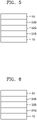
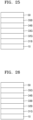
- FIGS. 2 to 31 each show a cross-sectional view of an OLED substrate according to one or more embodiments.
- the OLED substrate of FIG. 2 has a tandem structure in which a first electrode 10, a blue first emission unit 31B, a green second emission unit 32G, and a second electrode 50 are vertically stacked in sequence. That is, the OLED substrate of FIG. 2 includes one blue emission unit 31B and one green emission unit 32G.
- a color control unit 2 may be located above the second electrode 50. That is, the green second emission unit 32G of FIG. 2 may be located closer to the color control unit 2 than the blue first emission unit 31B.
- the first electrode 10 may be anode, which is a hole injection electrode, and the second electrode 50 may be a cathode, which is an electron injection electrode.
- the first electrode 10 may be a cathode, which is an electron injection electrode, and the second electrode 50 may be an anode, which is a hole injection electrode.
- a thin-film transistor (TFT) array substrate including a plurality of TFT (not shown) may be provided under the first electrode 10, and an OLED substrate 1 may be provided on the TFT array substrate.
- TFT thin-film transistor
- the first electrode 10 may be formed by, for example, applying a material for forming the first electrode 10 onto the substrate by using a deposition or sputtering method.
- the first electrode 10 may be an anode.
- the material for forming the first electrode 10 may include materials with a high work function to facilitate hole injection.
- the first electrode 10 may be a reflective electrode, a semi-transmissive electrode, or a transmissive electrode.
- the material for forming the first electrode 10 may be indium tin oxide (ITO), indium zinc oxide (IZO), tin oxide (SnO 2 ), or zinc oxide (ZnO).
- the material for forming the first electrode 10 may be metal, such as magnesium (Mg), aluminum (Al), silver (Ag), aluminum-lithium (Al-Li), calcium (Ca), magnesium-indium (Mg-In), or magnesium-silver (Mg-Ag).
- metal such as magnesium (Mg), aluminum (Al), silver (Ag), aluminum-lithium (Al-Li), calcium (Ca), magnesium-indium (Mg-In), or magnesium-silver (Mg-Ag).
- the first electrode 10 may have a single-layered structure or a multi-layered structure including a plurality of layers.
- the first electrode 10 may have a three-layered structure of ITO/Ag/ITO.
- the first electrode 10 may be a patterned element corresponding to each subpixel area and electrically connected to each TFT element of the TFT array substrate (not shown).
- the blue first emission unit 31B may include a blue luminescent compound (i.e., a blue light-emitting compound).
- the blue luminescent compound may include a blue phosphorescent compound, and a blue fluorescent compound (thermal activated delayed fluorescence (TADF) compound and/or prompt fluorescent compound).
- TADF thermal activated delayed fluorescence
- the blue luminescent compound may be an iridium-containing organometallic compound or a platinum-containing organometallic compound.
- the iridium-containing organometallic compound may include a ligand having a carbene moiety, and the carbon of the carbene moiety of the ligand and the iridium of the iridium-containing organometallic compound may be connected by a chemical bond.
- the blue luminescent compound may be a fluorescent compound including at least one boron (B) atom and at least one nitrogen (N) atom.
- the blue luminescent compound may include a C 6 -C 60 polycyclic group in which a 6-membered ring containing boron atom and a nitrogen atom as ring-forming atoms and a cyclic group are condensed with each other.
- the green second emission unit 32G may include a mixture of the first compound and the second compound as described herein.
- the second electrode 50 may be the cathode.
- a material for forming the second electrode 50 may be metal, an alloy, an electrically conductive compound, or a combination thereof, which have a relatively low work function.
- lithium (Li), magnesium (Mg), aluminum (Al), silver (Ag), aluminum-lithium (Al-Li), calcium (Ca), magnesium-indium (Mg-In), magnesium-silver (Mg-Ag), or the like may be used as the material for forming the second electrode 50.
- the second electrode 50 may be an unpatterned common electrode, or may be patterned with a plurality of electrode elements.
- a protective layer may additionally be located on the second electrode 50.
- the protective layer may include a transparent insulating material.
- the blue light emitted from the blue first emission unit 31B and the green light emitted from the green second emission unit 32G pass through the second electrode 50 and the color of each light is adjusted by the color control unit 2 and then the adjusted each light is emitted toward outside the light-emitting device.
- the OLED substrate of FIG. 3 has a tandem structure in which the first electrode 10, a green first emission unit 31G, a blue second emission unit 32B, and the second electrode 50 are vertically stacked in this order.
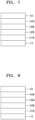
- the OLED substrate may include two blue emission units and one green emission unit, as illustrated in FIGS. 4 to 6 .
- the OLED substrate of FIG. 4 has a tandem structure in which the first electrode 10, the blue first emission unit 31B, the blue second emission unit 32B, a green third emission unit 33G, and the second electrode 50 are vertically stacked in this order.
- the OLED substrate of FIG. 5 has a tandem structure in which the first electrode 10, the blue first emission unit 31B, the green second emission unit 32G, a blue third emission unit 33B, and the second electrode 50 are vertically stacked in this order.
- the OLED substrate of FIG. 6 has a tandem structure in which the first electrode 10, the green first emission unit 31G, the blue second emission unit 32B, the blue third emission unit 33B, and the second electrode 50 are vertically stacked in this order.
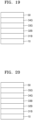
- the OLED substrate may include three blue emission units and one green emission unit, as illustrated in FIGS. 7 to 10 .
- the OLED substrate of FIG. 7 has a tandem structure in which the first electrode 10, the blue first emission unit 31B, the blue second emission unit 32B, the blue third emission unit 33B, a green fourth emission unit 34G, and the second electrode 50 are vertically stacked in this order.
- the OLED substrate of FIG. 8 has a tandem structure in which the first electrode 10, the blue first emission unit 31B, the blue second emission unit 32B, the green third emission unit 33G, a blue fourth emission unit 34B, and the second electrode 50 are vertically stacked in this order.
- the OLED substrate of FIG. 9 has a tandem structure in which the first electrode 10, the blue first emission unit 31B, the green second emission unit 32G, the blue third emission unit 33B, the blue fourth emission unit 34B and the second electrode 50 are vertically stacked in this order.
- the OLED substrate of FIG. 10 has a tandem structure in which the first electrode 10, the green first emission unit 31G, the blue second emission unit 32B, the blue third emission unit 33B, the blue fourth emission unit 34B, and the second electrode 50 are vertically stacked in this order.
- the OLED substrate may include four blue emission units and one green emission unit, as illustrated in FIGS. 11 to 15 .
- the OLED substrate of FIG. 11 has a tandem structure in which the first electrode 10, the blue first emission unit 31B, the blue second emission unit 32B, the blue third emission unit 33B, the blue fourth emission unit 34B, a green fifth emission unit 35G, and the second electrode 50 are vertically stacked in this order.
- the OLED substrate of FIG. 12 has a tandem structure in which the first electrode 10, the blue first emission unit 31B, the blue second emission unit 32B, a blue third emission unit 33B, a green fourth emission unit 34G, a blue fifth emission unit 35B, and the second electrode 50 are vertically stacked in this order.
- the OLED substrate of FIG. 13 has a tandem structure in which the first electrode 10, the blue first emission unit 31B, the blue second emission unit 32B, the green third emission unit 33G, the blue fourth emission unit 34B, the blue fifth emission unit 35B, and the second electrode 50 are vertically stacked in this order.
- the OLED substrate of FIG. 14 has a tandem structure in which the first electrode 10, the blue first emission unit 31B, the green second emission unit 32G, the blue third emission unit 33B, the blue fourth emission unit 34B, the blue fifth emission unit 35B, and the second electrode 50 are vertically stacked in this order.
- the OLED substrate of FIG. 15 has a tandem structure in which the first electrode 10, the green first emission unit 31G, the blue second emission unit 32B, the blue third emission unit 33B, the blue fourth emission unit 34B, the blue fifth emission unit 35B, and the second electrode 50 are vertically stacked in this order.
- the OLED substrate may include two blue emission units and two green emission units, as illustrated in FIGS. 16 to 19 .
- the OLED substrate of FIG. 16 has a tandem structure in which the first electrode 10, the green first emission unit 31G, the green second emission unit 32G, the blue third emission unit 33B, the blue fourth emission unit 34B, and the second electrode 50 are vertically stacked in this order.
- the OLED substrate of FIG. 17 has a tandem structure in which the first electrode 10, the green first emission unit 31G, the blue second emission unit 32B, the green third emission unit 33G, the blue fourth emission unit 34B, and the second electrode 50 are vertically stacked in this order.
- the OLED substrate of FIG. 18 has a tandem structure in which the first electrode 10, the blue first emission unit 31B, the green second emission unit 32G, the green third emission unit 33G, the blue fourth emission unit 34B, and the second electrode 50 are vertically stacked in this order.
- the OLED substrate of FIG. 19 has a tandem structure in which the first electrode 10, the blue first emission unit 31B, the blue second emission unit 32B, the green third emission unit 33G, the green fourth emission unit 34G, and the second electrode 50 are vertically stacked in this order.
- the OLED substrate may include three blue emission units and two green emission units, as illustrated in FIGS. 20 to 29 .
- the OLED substrate of FIG. 20 has a tandem structure in which the first electrode 10, the blue first emission unit 31B, the blue second emission unit 32B, the blue third emission unit 33B, the green fourth emission unit 34G, the green fifth emission unit 35G, and the second electrode 50 are vertically stacked in this order.
- the OLED substrate of FIG. 21 has a tandem structure in which the first electrode 10, the blue first emission unit 31B, the blue second emission unit 32B, the green third emission unit 33G, the blue fourth emission unit 34B, the green fifth emission unit 35G, and the second electrode 50 are vertically stacked in this order.
- the OLED substrate of FIG. 22 has a tandem structure in which the first electrode 10, the blue first emission unit 31B, the blue second emission unit 32B, the green third emission unit 33G, the green fourth emission unit 34G, the blue fifth emission unit 35B, and the second electrode 50 are vertically stacked in this order.
- the OLED substrate of FIG. 23 has a tandem structure in which the first electrode 10, the blue first emission unit 31B, the green second emission unit 32G, the blue third emission unit 33B, the blue fourth emission unit 34B, the green fifth emission unit 35G, and the second electrode 50 are vertically stacked in this order.
- the OLED substrate of FIG. 24 has a tandem structure in which the first electrode 10, the blue first emission unit 31B, the green second emission unit 32G, the blue third emission unit 33B, the green fourth emission unit 34G, the blue fifth emission unit 35B, and the second electrode 50 are vertically stacked in this order.
- the OLED substrate of FIG. 25 has a tandem structure in which the first electrode 10, the blue first emission unit 31B, the green second emission unit 32G, the green third emission unit 33G, the blue fourth emission unit 34B, the blue fifth emission unit 35B, and the second electrode 50 are vertically stacked in this order.
- the OLED substrate of FIG. 26 has a tandem structure in which the first electrode 10, the green first emission unit 31G, the blue second emission unit 32B, the blue third emission unit 33B, the blue fourth emission unit 34B, the green fifth emission unit 35G, and the second electrode 50 are vertically stacked in this order.
- the OLED substrate of FIG. 27 has a tandem structure in which the first electrode 10, the green first emission unit 31G, the blue second emission unit 32B, the blue third emission unit 33B, the green fourth emission unit 34G, the blue fifth emission unit 35B, and the second electrode 50 are vertically stacked in this order.
- the OLED substrate of FIG. 28 has a tandem structure in which the first electrode 10, the green first emission unit 31G, the blue second emission unit 32B, the green third emission unit 33G, the blue fourth emission unit 34B, the blue fifth emission unit 35B, and the second electrode 50 are vertically stacked in this order.
- the OLED substrate of FIG. 29 has a tandem structure in which the first electrode 10, the green first emission unit 31G, the green second emission unit 32G, the blue third emission unit 33B, the blue fourth emission unit 34B, the blue fifth emission unit 35B, and the second electrode 50 are vertically stacked in this order.
- the OLED substrates of FIGS. 3 to 29 may be understood by referring to the OLED substrate of FIG. 2 except that the number of emission units and/or the emission color has been changed.
- the OLED substrate of FIG. 30 has a tandem structure in which the first electrode 10, the blue first emission unit 31B, a first charge generation layer 61, the blue second emission unit 32B, a second charge generation layer 62, the blue third emission unit 33B, a third charge generation layer 63, the green fourth emission unit 34G, an electron transport region 40, and the second electrode 50 are vertically stacked in this order.
- Each of the first electrode 10, the blue first emission unit 31B, the blue second emission unit 32B, the blue third emission unit 33B, the green fourth emission unit 34G, and the second electrode 50 of FIG. 30 is the same as described in connection with FIG. 7 .
- the first charge generation layer 61 may supply charges to the blue first emission unit 31B and/or the blue second emission unit 32B, and the second charge generation layer 62 may supply charges to the blue second emission unit 32B and/or the blue third emission unit 33B, and the third charge generation layer 63 may supply charges to the blue third emission unit 33B and/or the green fourth emission unit 34G. Accordingly, the three blue emission units 31B, 32B, and 33B and one green emission unit 34G may emit light effectively.
- the electron transport region 40 may transfer electrons injected from the second electrode 50 to the green fourth emission unit 34G.
- the electron transport region 40 may include a hole-blocking layer, an electron transport layer, an electron injection layer, or a combination thereof.
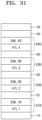
- the OLED substrate of FIG. 31 is a diagram illustrating details of the structure of each of the blue first emission unit 31B, the blue second emission unit 32B, the blue third emission unit 33B, and the green fourth emission unit 34G of the OLED substrate of FIG. 30 .
- the blue first emission unit 31B may include a first hole transport region HTL 1 and a blue first emission layer EML 1B
- the blue second emission unit 32B may include a second hole transport region HTL 2 and a blue second emission layer EML 2B
- the blue third emission unit 33B may include a third hole transport region HTL 3 and a blue third emission layer EML 3B
- the green fourth emission unit 34G may include a fourth hole transport region HTL 4 and a green fourth emission layer EML 4G.
- the first hole transport region HTL 1, the second hole transport region HTL 2, the third hole transport region HTL 3, and the fourth hole transport region HTL 4 may transfer holes to the blue first emission layer EML 1B, the blue second emission layer EML 2B, the blue third emission layer EML 3B, and the green fourth emission layer EML 4G, respectively.
- Each of the first hole transport region HTL 1, the second hole transport region HTL 2, the third hole transport region HTL 3, and the fourth hole transport region HTL 4 may include a hole injection layer, a hole transport layer, an electron-blocking layer, a buffer layer, or a combination thereof.
- the blue first emission layer EML 1B, the blue second emission layer EML 2B, and the blue third emission layer EML 3B may include the blue luminescent compound as described above, and the green fourth emission layer EML 4G may include a mixture of the first compound and the second compound as described herein.
- the green fourth emission layer EML 4G may include a host in addition to the mixture of the first compound and the second compound.
- the host may include a hole-transporting host, an electron-transporting host, a bipolar host, or a combination thereof.
- the green fourth emission layer EML 4G may be formed by i) co-depositing a first compound, a second compound, and a host or ii) a soluble process in which a solution including a first compound, a second compound, and a host is provided, and heat treatment is performed.
- the OLED substrate of FIGS. 2 to 6 and 8 to 29 may be variously changed with reference to the first charge generation layer 61, the second charge generation layer 62 and/or the third charge generation layer 63 of FIG. 30 and the first hole transport region HTL 1, the second hole transport region HTL 2, the third hole transport region HTL 3, the fourth hole transport region HTL 4, the blue first emission layer EML 1B, the blue second emission layer EML 2B, the blue third emission layer EML 3B, and/or the green fourth emission layer EML 4G of FIG. 31 .
- FIG. 32 is a cross-sectional view illustrating a light-emitting device according to one or more embodiments.
- the light-emitting device of FIG. 32 may include an OLED substrate 100 and a color control unit 200.
- the OLED substrate 100 may be the same as described above (for example, with reference to FIGS. 2 to 31 ).
- the color control unit 200 may include a first color control element 70a including a first quantum dot (green light emitting quantum dot (G-QD)) for green conversion, a second color control element 70b including a second quantum dot (red light emitting quantum dot (R-QD)) for red conversion, and a third color control element 75c for blue expression.
- the color control element is not limited to including a quantum dot.
- an inorganic material, an organic material, or a combination thereof that absorbs blue light or/and green light and converts the same to green light or red light may be used as the color control element.
- the color control unit 200 may further include a first color filter 80a located on the first color control element 70a and a second color filter 80b located on the second color control element 70b.
- the first color control element 70a may be a green-QD-containing layer, and may convert light generated from the OLED substrate 100 into green light G.
- the second color control element 70b may be a red-QD containing layer and may convert light generated from the OLED substrate 100 to red light R. Accordingly, the first color control element 70a may be referred to as a first color conversion element, and the second color control element 70b may be referred to as a second color conversion element.
- the color conversion element may include a resin material, a plurality of quantum dots, and a light scattering agent.
- the resin material may include, for example, a photoresist (PR) material.
- the third color control element 75c may be a color filter that optionally allows the blue (B) wavelength region of the light generated from the OLED substrate 100 to pass therethrough.
- the third color control element 75c may be a blue-color filter (C/F or CF).
- the third color control element 75c may be an absorption type color filter including a specific pigment(s) or quantum dot(s). The absorption type color filter may absorb light of wavelength band except light of the target wavelength band.
- the first color filter 80a may cut the remaining blue region wavelength of the light that has passed through the first color control element 70a.
- the second color filter 80b may cut the remaining blue and green regions wavelength of the light that has passed through the second color control element 70b.
- the first color filter 80a may be referred to as a blue-cut filter
- the second color filter 80b may be referred to as a blue and green-cut filter. Accordingly, color-controlling/filtering characteristics may be improved by the first color filter 80a and the second color filter 80b.
- a separate optical film may be additionally located on the third color control element 75c. Full colors of RGB may be realized by using the color control unit 200.
- the arrangement order or arrangement method of the RGB subpixels is an example, and may be variously changed.
- the first quantum dot that may be included in the first color control element 70a may be green-QD
- the second quantum dot that may be included in the second color control element 70b may be red-QD.
- a quantum dot refers to a semiconductor particle of a small sphere of nanometer (nm) size or a similar shape, and may have a size (diameter) of about several nm to several tens of nm.
- a quantum dot may have a monolithic structure or a core-shell structure, and in the case of a core-shell structure, the quantum dot may have a single shell structure or a multi-shell structure.
- a quantum dot may have a core portion (center) including a first semiconductor and a shell portion including a second semiconductor.
- a material for the core portion may be cadmium selenide (CdSe), cadmium telluride (CdTe), or cadmium sulfide (CdS), and a material for the shell portion may be zinc sulfide (ZnS).
- a non-cadmium-based quantum dot QD may be used. That is, various materials not including cadmium (Cd) may be applied to the quantum dot.
- the materials specifically presented here are exemplary, and other various materials may be applied to the quantum dot.
- the quantum dot may include at least one of a group II-VI semiconductor, a group III-V semiconductor, a group IV-VI semiconductor, a group IV semiconductor, or combination thereof.
- quantum dots are very small in size, quantum dots may exhibit a quantum confinement effect.
- electrons in the particle form a discontinuous energy state by the outer wall of the particle.
- the energy state of the electrons is relatively high, and the energy band gap increases. This effect is called as the quantum confinement effect.
- light such as ultraviolet rays or visible rays is incident on a quantum dot, light of various wavelengths may be generated.
- the wavelength of light generated from a quantum dot may be determined by the size, material, and/or structure of the particle (quantum dot).
- the quantum dot when light with a wavelength greater than the energy band width is incident on the quantum dot, the quantum dot may be excited by absorbing the energy of the light and may transit to a ground state while emitting light of a specific wavelength.
- the size of the quantum dot or, the core portion of the quantum dot
- light of a relatively short wavelength for example, bluish light or greenish light
- the size of the quantum dot or, the core portion of the quantum dot
- light of a relatively long wavelength for example, reddish light may be generated. Therefore, light of various colors may be realized according to the size of the quantum dot (or the core portion of the quantum dot).
- Quantum dot particles that may emit greenish light may be referred to as green light quantum dot particles
- quantum dot particles that may emit reddish light may be referred to as red light quantum dot particles
- green light quantum dot particles (or the core portion thereof) may be particles having a particle width (diameter) of about 2 nm to about 3 nm
- red light quantum dot particles (or the core portion thereof) may be particles having a particle width (diameter) of about 5 nm to about 6 nm.
- the emission wavelength may be controlled not only by the size (diameter) of the quantum dot but also by the material and structure.
- the first color control element 70a may be regarded as a kind of color filter that converts colors using quantum dots, the first color control element 70a may be referred to as a "first QD color filter”.
- the second color control element 70b may be referred to as a "second QD color filter”.
- the first color filter 80a and the second color filter 80b of a cut-off filter type may be formed in, for example, a distributed Bragg reflector (DBR) structure.
- DBR distributed Bragg reflector
- a DBR structure that passes or reflects only the desired wavelength band may be created by repeatedly stacking two material layers (dielectrics) having different refractive indices and adjusting the thickness and the number of layers to be stacked of the material layers.
- the DBR structure may be applied to the first color filter 80a and the second color filter 80b.
- a SiO 2 layer and a TiO 2 layer may be repeatedly stacked under ⁇ /4 condition (here, "A" represents a wavelength of light), and the thickness and the number of layers to be stacked may be controlled to increase a reflectance and a transmittance of a desired wavelength band.
- A represents a wavelength of light
- the thickness and the number of layers to be stacked may be controlled to increase a reflectance and a transmittance of a desired wavelength band.
- the DBR structure is well known, the detailed descriptions thereof are omitted herein.
- at least one of the first color filter 80a and the second color filter 80b may have a structure other than the DBR structure, for example, a high-contrast grating (HCG) structure.
- HCG high-contrast grating
- FIG. 33 is a cross-sectional view illustrating a light-emitting device according to one or more embodiments.
- the light-emitting device of FIG. 33 may include the OLED substrate 100 and a color control unit 201.
- the OLED substrate 100 may be the same as described above (for example, with reference to FIGS. 2 to 31 ).
- the color control unit 201 of FIG. 33 is the same as the color control unit 200 of FIG. 32 except that a light scattering element 71c located between the third color control element 75c and the OLED substrate 100 is added.
- the light scattering element 71c may include a resin material and a light scattering agent.
- the resin material may include a photoresist (PR) material.
- the light scattering agent may include, for example, titanium oxide (TiO 2 ).
- the first color control element 70a and the second color control element 70b may each include a light scattering agent. Accordingly, by positioning the light scattering element 71c under the third color control element 75c, the impression of colors may be balanced. In other words, change in visibility in a RGB region may be reduced.
- FIG. 34 is a cross-sectional view illustrating a light-emitting device according to one or more embodiments.
- the light-emitting device of FIG. 34 may include the OLED substrate 100 and a color control unit 202.
- the OLED substrate 100 may be the same as described above (for example, with reference to FIGS. 2 to 31 ).
- the color control unit 202 of FIG. 34 is the same as the color control unit 200 of FIG. 32 except that a blue-QD(blue light-emitting quantum dot)-containing layer as the third color control element 70c is used instead of the blue-color filter (B-C/F) as the third color control element 75c, and a third color filter 80c disposed on the third color control element 75c may be further included.
- the third color filter 80c may optionally be included.
- the third color control element 70c may convert the light generated from the OLED substrate 100 into blue light B. Accordingly, the third color control element 70c may be referred to as a third color conversion element.
- the third color control element 70c may include a resin material, quantum dots, and a light scattering agent.
- the third color filter 80c may cut the remaining green region wavelength of the light that has passed through the third color control element 70c. That is, the third color filter 80c may be a green-cut filter.
- FIG. 35 is a cross-sectional view illustrating a light-emitting device according to one or more embodiments.
- the light-emitting device of FIG. 35 may include the OLED substrate 100 and a color control unit 203.
- the OLED substrate 100 may be the same as described above (for example, with reference to FIGS. 2 to 31 ).
- the color control unit 203 of FIG. 35 is the same as the color control unit 201 of FIG. 33 , except that a first color filter 75a and a second color filter 75b are used instead of the first color filter 80a and the second color filter 80b that are of a cut-off filter type, respectively.
- An absorption-type green-color filter may be used as the first color filter 75a, and an absorption-type red-color filter (R-C/F) may be used as the second color filter 75b.
- the green-color filter 75a may selectively transmit light in the green wavelength region and absorb light in the other wavelength region.
- the red-color filter 75b may selectively transmit light in the red wavelength region and absorb light in the other wavelength region.
- the color control unit 203 of the present embodiment uses absorption type color filters 75a, 75b, and 75c respectively for the R-subpixel, G-subpixel and B-subpixel regions.
- the third color control element 70c containing the blue-QD in FIG. 34 may be used instead of the light scattering element 71c.
- the light-emitting device may further include a fourth sub-pixel, in addition to a R-sub-pixel (first sub-pixel), a G-sub-pixel (second sub-pixel), and a B-sub-pixel (third sub-pixel).
- the fourth sub-pixel may be configured to exhibit a color (a fourth color) other than R, G, and B.
- the other color (fourth color) may be, for example, cyan (C).
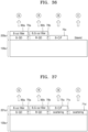
- FIGS. 36 to 39 Embodiments of the light-emitting device further including the fourth sub-pixel area are illustrated in FIGS. 36 to 39 .
- 100a denotes an OLED substrate
- 200a, 201a, 202a, and 203a denote color control units.
- the present embodiment is similar to the configuration described in connection with FIG. 32 , except that a portion of the OLED substrate 100a is a blank region.
- the blank region may correspond to the fourth sub-pixel region, and cyan (C) color may be exhibited from the blank region.
- the present embodiment is similar to the configuration described in connection with FIG. 33 , except that a light scattering element 71d may be further included in the fourth sub-pixel area of the OLED substrate 100a.
- the light scattering element 71c provided under the third color control element 75c is a first light scattering element, and the light scattering element 71d provided in the fourth sub-pixel area may be referred to as a second light scattering element.
- the first light scattering element 71c and the second light scattering element 71d may have the same or similar material composition.
- the present embodiment is similar to the configuration described in connection with FIG. 34 , except that a light scattering element 71d may be further included in the fourth sub-pixel area of the OLED substrate 100a.
- the present embodiment is similar to the configuration described in connection with FIG. 35 , except that the light scattering element 71d may be further included in the fourth sub-pixel area of the OLED substrate 100a.
- the arrangement order and method of the R-subpixel (the first subpixel), the G-subpixel (the second subpixel), the B-subpixel (the third subpixel), and the C-subpixel (the fourth subpixel) are illustrative only, and various alterations may be made.
- the R, G, B, and C subpixel regions may be arranged such that a square shape matrix form may be formed when viewed from a top view.
- the color exhibited in the C-subpixel (the fourth subpixel) region may be any other color other than cyan (C).
- FIG. 40 shows a graph of a PL quantum yield (%) according to the wavelength (nm) of a green-QD containing color conversion element and a red-QD containing color conversion element which may be applicable to a light-emitting device according to one or more embodiments.
- the green-QD containing color conversion element provides the PL quantum yield up to approximately the green wavelength region
- the red-QD containing color conversion element provides the PL quantum yield up to approximately the red wavelength region.
- the green-QD containing color conversion element and the red-QD containing color conversion element may be applicable to the first color control element 70a and the second color control element 70b of FIGS. 32 to 39 , respectively.
- FIG. 41 shows a graph of transmittance (%) according to the wavelength of a green-QD containing color conversion element and a red-QD containing color conversion element which may be applicable to a light-emitting device according to one or more embodiments.
- the green-QD containing color conversion element provides the transmittance from a wavelength corresponding to approximately in the green region
- the red-QD containing color conversion element provides the transmittance from a wavelength corresponding to approximately in the red region.
- FIG. 42 shows a graph of transmittance (%) according to wavelength of an absorption type color filter that may be applicable to a light-emitting device according to one or more embodiments.
- Results for absorption type red-color filter (CF-Red), absorption type green-color filter (CF-Green) and absorption type blue-color filter (CF-Blue) are included.
- results for absorption type low reflection red-color filter (low reflection R), absorption type low reflection green-color filter (low reflection G) and absorption type low reflection blue-color filter (low reflection B) are also included.
- the term "low reflection" in the absorption type low reflection red-color filter refers to the case where the reflectance is relatively lower than that of the absorption type red-color filter.
- This description is also applicable to the low reflection green-color filter and the low reflection blue-color filter.
- the reflectance and transmittance thereof may be appropriately adjusted.
- the absorption type low reflection green-color filter, the absorption type low reflection red-color filter, and the absorption type low reflection blue-color filter may also be applied to the first color filter 75a, the second color filter 75b and the third color control element 75c, respectively.
- the reflectivity on a panel may be reduced, so that the contrast ratio in the bright room can be increased without a circular polarizer.
- FIG. 43 shows a graph showing a difference in spectral radiance when a light scattering agent is applied to blue light and when no light scattering agent is applied.
- OLED substrates A, B, C, 1 and 2 each having the structure illustrated in FIG. 31 , were fabricated.
- OLED substrates A, B, C, 1 and 2 are identical to each other except that, for each OLED substrate, the dopant compound(s) included in the EML4G of the green fourth emission unit 34G is as shown in Table 1.
- Table 1 Each of Ir1, Ir2 and Pt1 in Table 1 emit a green light.
- the luminescence efficiency (candela per ampere, cd/A) and lifespan (LT 95 , hr, relative %) of each of OLED substrates A, B, C, 1 and 2 were measured using a current-voltmeter (Keithley 2400) and a luminance meter (Minolta Cs-1000A), under the luminance conditions described in in Table 1. Results thereof are shown as a relative value (%) in Table 1.
- the Lifespan (LT 95 ) refers to a time that is taken for the luminance to become 95% with respect to the initial luminance of 100%.
- EML4G is consisted of the dopant compound(s) and the hosts.
- FIG. 44 shows a graph of the EL spectrum of OLED substrate 2. Referring to FIG. 44 , it can be seen that OLED substrate 2 emits light in which blue light is mixed with green light.
- Light Emitting Device 1 having the structure illustrated in FIG. 35 was manufactured including: OLED substrate 2 as the OLED substrate 100;
- FIG. 45 shows a graph of the PL spectrum of the Light Emitting Device 1. As illustrated in FIG. 45 , it can be seen that the blue light and green light emitted from OLED substrate 2 are effectively emitted in the form of red light, green light, and blue light after passing through the color control unit 203.
- the light-emitting devices according to the embodiments described above may be applicable to various electronic apparatuses such as display apparatus.
- the light emitting devices may be usefully applied to small-sized electronic devices such as portable devices and wearable devices, and medium- to large-sized electronic devices such as home appliances.
- C 1 -C 60 alkyl group refers to a linear or branched saturated aliphatic hydrocarbons monovalent group having 1 to 60 carbon atoms
- C 1 -C 60 alkylene group refers to a divalent group having the same structure as the C 1 -C 60 alkyl group.
- Examples of the C 1 -C 60 alkyl group, the C 1 -C 20 alkyl group, and/or the C 1 -C 10 alkyl group are a methyl group, an ethyl group, an n-propyl group, an isopropyl group, an n-butyl group, a sec-butyl group, an isobutyl group, a tert-butyl group, an n-pentyl group, a tert-pentyl group, a neopentyl group, an isopentyl group, a sec-pentyl group, a 3-pentyl group, a sec-isopentyl group, an n-hexyl group, an isohexyl group, a sec-hexyl group, a tert-hexyl group, an n-heptyl group, an isoheptyl group, a sec-heptyl group, a ter
- C 1 -C 60 alkoxy group refers to a monovalent group represented by -OA 101 (wherein A 101 is the C 1 -C 60 alkyl group), and examples thereof are a methoxy group, an ethoxy group, a propoxy group, a butoxy group, and a pentoxy group.
- C 1 -C 60 alkylthio group refers to a monovalent group represented by -SA 101 (wherein A 101 is the C 1 -C 60 alkyl group).
- C 2 -C 60 alkenyl group refers to a hydrocarbon group formed by substituting at least one carbon-carbon double bond in the middle or at the terminus of the C 2 -C 60 alkyl group, and examples thereof include an ethenyl group, a propenyl group, and a butenyl group.
- C 2 -C 60 alkenylene group refers to a divalent group having the same structure as the C 2 -C 60 alkenyl group.
- C 2 -C 60 alkynyl group refers to a hydrocarbon group formed by substituting at least one carbon-carbon triple bond in the middle or at the terminus of the C 2 -C 60 alkyl group, and examples thereof include an ethynyl group, and a propynyl group.
- C 2 -C 60 alkynylene group refers to a divalent group having the same structure as the C 2 -C 60 alkynyl group.
- C 3 -C 10 cycloalkyl group refers to a monovalent saturated hydrocarbon cyclic group having 3 to 10 carbon atoms
- C 3 -C 10 cycloalkylene group refers to a divalent group having the same structure as the C 3 -C 10 cycloalkyl group.
- Examples of the C 3 -C 10 cycloalkyl group are a cyclopropyl group, a cyclobutyl group, a cyclopentyl, cyclohexyl group, a cycloheptyl group, a cyclooctyl group, an adamantanyl group, a norbornanyl group (or a bicyclo[2.2.1]heptyl group), a bicyclo[1.1.1]pentyl group, a bicyclo[2.1.1]hexyl group, and a bicyclo[2.2.2]octyl group.
- C 1 -C 10 heterocycloalkyl group refers to a monovalent saturated cyclic group that includes at least one heteroatom selected from N, O, P, Si, S, Se, Ge, and B as a ring-forming atom and 1 to 10 carbon atoms
- C 1 -C 10 heterocycloalkylene group refers to a divalent group having the same structure as the C 1 -C 10 heterocycloalkyl group.
- Examples of the C 1 -C 10 heterocycloalkyl group are a silolanyl group, a silinanyl group, tetrahydrofuranyl group, a tetrahydro-2H-pyranyl group, and a tetrahydrothiophenyl group.
- C 3 -C 10 cycloalkenyl group refers to a monovalent monocyclic group that has 3 to 10 carbon atoms and at least one carbon-carbon double bond in the ring thereof and no aromaticity, and non-limiting examples thereof include a cyclopentenyl group, a cyclohexenyl group, and a cycloheptenyl group.
- C 3 -C 10 cycloalkenylene group refers to a divalent group having the same structure as the C 3 -C 10 cycloalkenyl group.
- C 1 -C 10 heterocycloalkenyl group refers to a monovalent monocyclic group that has at least one heteroatom selected from N, O, P, Si, S, Se, Ge, and B as a ring-forming atom, 1 to 10 carbon atoms, and at least one double bond in its ring.
- Examples of the C 1 -C 10 heterocycloalkenyl group are a 2,3-dihydrofuranyl group, and a 2,3-dihydrothiophenyl group.
- C 1 -C 10 heterocycloalkenylene group refers to a divalent group having the same structure as the C 1 -C 10 heterocycloalkenyl group.
- C 6 -C 60 aryl group refers to a monovalent group having a carbocyclic aromatic system having 6 to 60 carbon atoms
- C 6 -C 60 arylene group refers to a divalent group having a carbocyclic aromatic system having 6 to 60 carbon atoms.
- Examples of the C 6 -C 60 aryl group include a phenyl group, a naphthyl group, an anthracenyl group, a phenanthrenyl group, a pyrenyl group, and a chrysenyl group.
- the C 6 -C 60 aryl group and the C 6 -C 60 arylene group each include two or more rings, the rings may be fused to each other.
- C 7 -C 60 alkyl aryl group refers to a C 6 -C 60 aryl group substituted with at least one C 1 -C 60 alkyl group.
- C 7 -C 60 aryl alkyl group refers to a C 1 -C 60 alkyl group substituted with at least one C 6 -C 60 aryl group.
- C 1 -C 60 heteroaryl group refers to a monovalent group that includes at least one heteroatom selected from N, O, P, Si, S, Se, Ge, and B as a ring-forming atom and a cyclic aromatic system having 1 to 60 carbon atoms
- C 1 -C 60 heteroarylene group refers to a divalent group that includes at least one heteroatom selected from N, O, P, Si, S, Se, Ge, and B as a ring-forming atom and a carbocyclic aromatic system having 1 to 60 carbon atoms.
- Examples of the C 1 -C 60 heteroaryl group include a pyridinyl group, a pyrimidinyl group, a pyrazinyl group, a pyridazinyl group, a triazinyl group, a quinolinyl group, and an isoquinolinyl group.
- the C 1 -C 60 heteroaryl group and the C 1 -C 60 heteroarylene group each include two or more rings, the rings may be fused to each other.
- C 2 -C 60 alkyl heteroaryl group refers to a C 1 -C 60 heteroaryl group substituted with at least one C 1 -C 60 alkyl group.
- C 2 -C 60 heteroaryl alkyl group refers to a C 1 -C 60 alkyl group substituted with at least one C 1 -C 60 heteroaryl group.
- C 6 -C 60 aryloxy group indicates -OA 102 (wherein A 102 indicates the C 6 -C 60 aryl group), and the term “C 6 -C 60 arylthio group” as used herein indicates -SA 103 (wherein A 103 indicates the C 6 -C 60 aryl group).
- C 1 -C 60 heteroaryloxy group indicates -OA 102' (wherein A 102' indicates the C 1 -C 60 heteroaryl group), and the term C 1 -C 60 heteroarylthio group” as used herein indicates -SA 103' (wherein A 103' indicates the C 1 -C 60 heteroaryl group).
- the term "monovalent non-aromatic condensed polycyclic group” as used herein refers to a monovalent group (for example, having 8 to 60 carbon atoms) having two or more rings condensed to each other, only carbon atoms as ring-forming atoms, and no aromaticity in its entire molecular structure.
- Examples of the monovalent non-aromatic condensed polycyclic group include a fluorenyl group.
- divalent non-aromatic condensed polycyclic group refers to a divalent group having the same structure as the monovalent non-aromatic condensed polycyclic group described above.
- the term "monovalent non-aromatic condensed heteropolycyclic group” as used herein refers to a monovalent group (for example, having 1 to 60 carbon atoms) having two or more rings condensed to each other, at least one heteroatom selected from N, O, P, Si, S, Se, Ge, and B, other than carbon atoms, as a ring-forming atom, and no aromaticity in its entire molecular structure.
- Examples of the monovalent non-aromatic condensed heteropolycyclic group include a carbazolyl group.
- divalent non-aromatic condensed heteropolycyclic group refers to a divalent group having the same structure as the monovalent non-aromatic condensed heteropolycyclic group described above.
- C 5 -C 30 carbocyclic group refers to a saturated or unsaturated cyclic group having, as a ring-forming atom, 5 to 30 carbon atoms only.
- the C 5 -C 30 carbocyclic group may be a monocyclic group or a polycyclic group.
- Examples of the "C 5 -C 30 carbocyclic group (unsubstituted or substituted with at least one R 10a )" used herein are an adamantane group, a norbornene group, a bicyclo[1.1.1]pentane group, a bicyclo[2.1.1]hexane group, a bicyclo[2.2.1]heptane(norbornane) group, a bicyclo[2.2.2]octane group, a cyclopentane group, a cyclohexane group, a cyclohexene group, a benzene group, a naphthalene group, an anthracene group, a phenanthrene group, a triphenylene group, a pyrene group, a chrysene group, a 1,2,3,4-tetrahydronaphthalene group, a cyclopentadiene group, and a fluorene group
- C 1 -C 30 heterocyclic group refers to a saturated or unsaturated cyclic group having, as a ring-forming atom, at least one heteroatom selected from N, O, P, Si, S, Se, Ge, and B other than 1 to 30 carbon atoms.
- the C 1 -C 30 heterocyclic group may be a monocyclic group or a polycyclic group.
- the "C 1 -C 30 heterocyclic group (unsubstituted or substituted with at least one R 10a )" may be, for example, a thiophene group, a furan group, a pyrrole group, a silole group, borole group, a phosphole group, a selenophene group, a germole group, a benzothiophene group, a benzofuran group, an indole group, a benzosilole group, a benzoborole group, a benzophosphole group, a benzoselenophene group, a benzogermole group, a dibenzothiophene group, a dibenzofuran group, a carbazole group, a dibenzosilole group, a dibenzoborole group, a dibenzophosphole group, a dibenzoselenophene group, a dibenzogermole group, a dibenzo
- Examples of the "C 5 -C 30 carbocyclic group” and the "C 1 -C 30 heterocyclic group” as used herein are i) a first ring, ii) a second ring, iii) a condensed ring in which two or more first rings are condensed with each other, iv) a condensed ring in which two or more second rings are condensed with each other, or v) a condensed ring in which at least one first ring is condensed with at least one second ring,
- fluorinated C 1 -C 60 alkyl group (or a fluorinated C 1 -C 20 alkyl group or the like)
- fluorinated C 3 -C 10 cycloalkyl group "fluorinated C 1 -C 10 heterocycloalkyl group”
- fluorinated phenyl group respectively indicate a C 1 -C 60 alkyl group (or a C 1 -C 20 alkyl group or the like), a C 3 -C 10 cycloalkyl group, a C 1 -C 10 heterocycloalkyl group, and a phenyl group, each substituted with at least one fluoro group (-F).
- fluorinated C 1 alkyl group that is, a fluorinated methyl group
- fluorinated C 1 alkyl group includes -CF 3 , - CF 2 H, and -CFH 2 .
- the "fluorinated C 1 -C 60 alkyl group (or, a fluorinated C 1 -C 20 alkyl group, or the like)", "the fluorinated C 3 -C 10 cycloalkyl group", “the fluorinated C 1 -C 10 heterocycloalkyl group”, or “the fluorinated a phenyl group” may be i) a fully fluorinated C 1 -C 60 alkyl group (or, a fully fluorinated C 1 -C 20 alkyl group, or the like), a fully fluorinated C 3 -C 10 cycloalkyl group, a fully fluorinated C 1 -C 10 heterocycloalkyl group, or a fully fluorinated pheny
- deuterated C 1 -C 60 alkyl group (or a deuterated C 1 -C 20 alkyl group or the like)
- deuterated C 3 -C 10 cycloalkyl group "deuterated C 1 -C 10 heterocycloalkyl group”
- deuterated phenyl group respectively indicate a C 1 -C 60 alkyl group (or a C 1 -C 20 alkyl group or the like), a C 3 -C 10 cycloalkyl group, a C 1 -C 10 heterocycloalkyl group, and a phenyl group, each substituted with at least one deuterium.
- the "deuterated C 1 alkyl group (that is, the deuterated methyl group)" may include -CD 3 , - CD 2 H, and -CDH 2 , and examples of the “deuterated C 3 -C 10 cycloalkyl group” are, for example, Formula 10-501 and the like.
- the "deuterated C 1 -C 60 alkyl group (or, the deuterated C 1 -C 20 alkyl group or the like)", “the deuterated C 3 -C 10 cycloalkyl group”, “the deuterated C 1 -C 10 heterocycloalkyl group”, or “the deuterated phenyl group” may be i) a fully deuterated C 1 -C 60 alkyl group (or, a fully deuterated C 1 -C 20 alkyl group or the like), a fully deuterated C 3 -C 10 cycloalkyl group, a fully deuterated C 1 -C 10 heterocycloalkyl group, or a fully deuterated phenyl group, in which, in each group, all hydrogen included therein are substituted with deuterium, or ii) a partially deuterated C 1 -C 60 alkyl group (or, a partially deuterated C 1 -C 20 alkyl group or the like), a partially deuterated
- (C 1 -C 20 alkyl) 'X' group refers to a 'X' group that is substituted with at least one C 1 -C 20 alkyl group.
- the term "(C 1 -C 20 alkyl)C 3 -C 10 cycloalkyl group” as used herein refers to a C 3 -C 10 cycloalkyl group substituted with at least one C 1 -C 20 alkyl group
- the term “(C 1 -C 20 alkyl)phenyl group” as used herein refers to a phenyl group substituted with at least one C 1 -C 20 alkyl group.
- An example of a (C 1 alkyl)phenyl group is a toluyl group.
- Q 1 to Q 9 , Q 11 to Q 19 , Q 21 to Q 29 , and Q 31 to Q 39 may each independently be: hydrogen, deuterium, -F, -Cl, -Br, -I, -SF 5 , a hydroxyl group, a cyano group, a nitro group, a substituted or unsubstituted C 1 -C 60 alkyl group, a substituted or unsubstituted C 2 -C 60 alkenyl group, a substituted or unsubstituted C 2 -C 60 alkynyl group, a substituted or unsubstituted C 1 -C 60 alkoxy group, a substituted or unsubstituted C 1 -C 60 alkylthio group, a substituted or unsubstituted C 3 -C 10 cycloalkyl group, a substituted or unsubstituted C 1 -C 10 heterocycloalkyl group, a substituted or unsub
- Q 1 to Q 9 , Q 11 to Q 19 , Q 21 to Q 29 and Q 31 to Q 39 described herein may each independently be:
- the light-emitting device described above has high luminescence efficiency and long lifespan. Accordingly, an electronic apparatus including the same can be a high-quality electronic apparatus.
Landscapes
- Chemical & Material Sciences (AREA)
- Physics & Mathematics (AREA)
- Optics & Photonics (AREA)
- Crystallography & Structural Chemistry (AREA)
- Inorganic Chemistry (AREA)
- Engineering & Computer Science (AREA)
- Materials Engineering (AREA)
- Electroluminescent Light Sources (AREA)
- General Physics & Mathematics (AREA)
Applications Claiming Priority (1)
| Application Number | Priority Date | Filing Date | Title |
|---|---|---|---|
| KR1020210124268A KR102760051B1 (ko) | 2021-09-16 | 2021-09-16 | 발광 장치 및 이를 포함한 전자 기기 |
Publications (1)
| Publication Number | Publication Date |
|---|---|
| EP4152913A1 true EP4152913A1 (de) | 2023-03-22 |
Family
ID=83319320
Family Applications (1)
| Application Number | Title | Priority Date | Filing Date |
|---|---|---|---|
| EP22195349.0A Pending EP4152913A1 (de) | 2021-09-16 | 2022-09-13 | Lichtemittierende vorrichtung und elektronische vorrichtung damit |
Country Status (4)
| Country | Link |
|---|---|
| US (1) | US20230165095A1 (de) |
| EP (1) | EP4152913A1 (de) |
| KR (1) | KR102760051B1 (de) |
| CN (1) | CN115835752A (de) |
Families Citing this family (1)
| Publication number | Priority date | Publication date | Assignee | Title |
|---|---|---|---|---|
| CN115440908A (zh) * | 2021-06-03 | 2022-12-06 | 三星电子株式会社 | 组合物、包括该组合物的层、包括该组合物的发光器件、和包括该发光器件的电子设备 |
Citations (2)
| Publication number | Priority date | Publication date | Assignee | Title |
|---|---|---|---|---|
| US20200251040A1 (en) * | 2017-06-23 | 2020-08-06 | Samsung Electronics Co., Ltd. | Display apparatus |
| US20210020847A1 (en) * | 2019-07-17 | 2021-01-21 | Lg Display Co., Ltd | Organic compound, organic light emitting diode and organic light emitting device including the organic compound |
Family Cites Families (4)
| Publication number | Priority date | Publication date | Assignee | Title |
|---|---|---|---|---|
| KR102718623B1 (ko) * | 2016-12-16 | 2024-10-16 | 가부시키가이샤 한도오따이 에네루기 켄큐쇼 | 유기 금속 착체, 발광 소자, 발광 장치, 전자 기기, 및 조명 장치 |
| KR102477097B1 (ko) * | 2017-06-23 | 2022-12-13 | 삼성전자주식회사 | 디스플레이 장치 |
| KR102837685B1 (ko) * | 2019-11-01 | 2025-07-23 | 삼성디스플레이 주식회사 | 양자점-함유 복합체, 이를 포함한 발광 소자, 광학 부재 및 장치 |
| KR20210098361A (ko) * | 2020-01-30 | 2021-08-10 | 삼성디스플레이 주식회사 | 발광 소자 및 전자 장치 |
-
2021
- 2021-09-16 KR KR1020210124268A patent/KR102760051B1/ko active Active
-
2022
- 2022-09-13 EP EP22195349.0A patent/EP4152913A1/de active Pending
- 2022-09-15 US US17/932,421 patent/US20230165095A1/en active Pending
- 2022-09-16 CN CN202211128037.3A patent/CN115835752A/zh active Pending
Patent Citations (2)
| Publication number | Priority date | Publication date | Assignee | Title |
|---|---|---|---|---|
| US20200251040A1 (en) * | 2017-06-23 | 2020-08-06 | Samsung Electronics Co., Ltd. | Display apparatus |
| US20210020847A1 (en) * | 2019-07-17 | 2021-01-21 | Lg Display Co., Ltd | Organic compound, organic light emitting diode and organic light emitting device including the organic compound |
Non-Patent Citations (2)
| Title |
|---|
| BENJAMIN HELEN ET AL: "Unusual dual-emissive heteroleptic iridium complexes incorporating TADF cyclometalating ligands", DALTON TRANSACTION, vol. 49, no. 7, 31 January 2020 (2020-01-31), UK, pages 2190 - 2208, XP055879503, ISSN: 1477-9226, DOI: 10.1039/C9DT04672K * |
| GUTI�RREZ-LLORENTE ARACELI ED - BULOVI VLADIMIR ET AL: "Effect of an assistant dopant on the vibrational satellites of a phosphorescent emitter: Application to solution-processed single-layer white organic light-emitting diodes", ORGANIC ELECTRONICS, ELSEVIER, AMSTERDAM, NL, vol. 84, 28 April 2020 (2020-04-28), XP086183934, ISSN: 1566-1199, [retrieved on 20200428], DOI: 10.1016/J.ORGEL.2020.105786 * |
Also Published As
| Publication number | Publication date |
|---|---|
| CN115835752A (zh) | 2023-03-21 |
| KR20230040758A (ko) | 2023-03-23 |
| KR102760051B1 (ko) | 2025-01-24 |
| US20230165095A1 (en) | 2023-05-25 |
Similar Documents
| Publication | Publication Date | Title |
|---|---|---|
| EP3663308B1 (de) | Organometallische verbindung, organische lichtemittierende vorrichtung mit der organometallischen verbindung und diagnostische zusammensetzung mit der organometallischen verbindung | |
| TWI781123B (zh) | 用於有機電激發光裝置之材料 | |
| KR102167199B1 (ko) | 유기 전계발광 소자 | |
| EP3617215A1 (de) | Organometallische verbindung, organische lichtemittierende vorrichtung mit der organometallischen verbindung und diagnostische zusammensetzung mit der organometallischen verbindung | |
| CN110003281A (zh) | 有机金属化合物、包括其的有机发光器件、和包括其的诊断组合物 | |
| CN110066296A (zh) | 有机金属化合物、以及包括其的有机发光器件和诊断组合物 | |
| CN109963857A (zh) | 作为用于有机电致发光器件(oled)的材料的双苯并呋喃稠合的2,8-二氨基茚并[1,2-b]芴衍生物和相关化合物 | |
| CN107683281A (zh) | 用于有机电致发光器件的材料 | |
| TW201726589A (zh) | 用於電子裝置之化合物 | |
| TW201726660A (zh) | 有機電發光裝置用的材料 | |
| CN110872326A (zh) | 有机金属化合物、包括该有机金属化合物的有机发光器件和诊断组合物 | |
| EP3392258B1 (de) | Organometallische verbindung, organische lichtemittierende vorrichtung mit der organometallischen verbindung und diagnostische zusammensetzung mit der organometallischen verbindung | |
| EP3862360B1 (de) | Organometallische verbindung, organische lichtemittierende vorrichtung damit und elektronische einrichtung mit der organischen lichtemittierenden vorrichtung | |
| CN111747990A (zh) | 有机金属化合物、包括其的有机发光器件和包括其的诊断组合物 | |
| EP3865553A1 (de) | Organometallische verbindung, organische lichtemittierende vorrichtung damit und elektronische einrichtung mit der organischen lichtemittierenden vorrichtung | |
| CN110573515A (zh) | 用于电子器件的化合物 | |
| EP3772517B1 (de) | Organometallische verbindung, organische lichtemittierende vorrichtung damit und diagnosezusammensetzung damit | |
| EP3725793B1 (de) | Organometallische verbindung, organische lichtemittierende vorrichtung mit der organometallischen verbindung und diagnostische zusammensetzung mit der organometallischen verbindung | |
| EP3395823B1 (de) | Organometallische verbindung, organische lichtemittierende vorrichtung damit und diagnosezusammensetzung mit der organometallischen verbindung | |
| EP3722301B1 (de) | Organometallische verbindung, organische lichtemittierende vorrichtung mit der organometallischen verbindung, diagnostische zusammensetzung mit der organometallischen verbindung | |
| TW202136181A (zh) | 有機電致發光裝置用的材料 | |
| EP4152913A1 (de) | Lichtemittierende vorrichtung und elektronische vorrichtung damit | |
| CN115466616A (zh) | 组合物、包括该组合物的层、包括该组合物的发光器件、和包括该发光器件的电子设备 | |
| CN112812086B (zh) | 有机金属络合物的辅助配体以及包括其的装置和调配物 | |
| TWI802656B (zh) | 用於有機電致發光裝置之材料 |
Legal Events
| Date | Code | Title | Description |
|---|---|---|---|
| PUAI | Public reference made under article 153(3) epc to a published international application that has entered the european phase |
Free format text: ORIGINAL CODE: 0009012 |
|
| STAA | Information on the status of an ep patent application or granted ep patent |
Free format text: STATUS: THE APPLICATION HAS BEEN PUBLISHED |
|
| AK | Designated contracting states |
Kind code of ref document: A1 Designated state(s): AL AT BE BG CH CY CZ DE DK EE ES FI FR GB GR HR HU IE IS IT LI LT LU LV MC MK MT NL NO PL PT RO RS SE SI SK SM TR |
|
| STAA | Information on the status of an ep patent application or granted ep patent |
Free format text: STATUS: REQUEST FOR EXAMINATION WAS MADE |
|
| 17P | Request for examination filed |
Effective date: 20230329 |
|
| RBV | Designated contracting states (corrected) |
Designated state(s): AL AT BE BG CH CY CZ DE DK EE ES FI FR GB GR HR HU IE IS IT LI LT LU LV MC MK MT NL NO PL PT RO RS SE SI SK SM TR |
|
| P01 | Opt-out of the competence of the unified patent court (upc) registered |
Effective date: 20230519 |
|
| STAA | Information on the status of an ep patent application or granted ep patent |
Free format text: STATUS: EXAMINATION IS IN PROGRESS |
|
| 17Q | First examination report despatched |
Effective date: 20240819 |
|
| RAP1 | Party data changed (applicant data changed or rights of an application transferred) |
Owner name: SAMSUNG DISPLAY CO., LTD. |