EP4152608A1 - Phase and amplitude error correction in a transmission circuit - Google Patents
Phase and amplitude error correction in a transmission circuit Download PDFInfo
- Publication number
- EP4152608A1 EP4152608A1 EP22196188.1A EP22196188A EP4152608A1 EP 4152608 A1 EP4152608 A1 EP 4152608A1 EP 22196188 A EP22196188 A EP 22196188A EP 4152608 A1 EP4152608 A1 EP 4152608A1
- Authority
- EP
- European Patent Office
- Prior art keywords
- voltage
- circuit
- phase correction
- modulated
- target
- Prior art date
- Legal status (The legal status is an assumption and is not a legal conclusion. Google has not performed a legal analysis and makes no representation as to the accuracy of the status listed.)
- Pending
Links
Images






Classifications
-
- H—ELECTRICITY
- H03—ELECTRONIC CIRCUITRY
- H03F—AMPLIFIERS
- H03F3/00—Amplifiers with only discharge tubes or only semiconductor devices as amplifying elements
- H03F3/20—Power amplifiers, e.g. Class B amplifiers, Class C amplifiers
- H03F3/24—Power amplifiers, e.g. Class B amplifiers, Class C amplifiers of transmitter output stages
- H03F3/245—Power amplifiers, e.g. Class B amplifiers, Class C amplifiers of transmitter output stages with semiconductor devices only
-
- H—ELECTRICITY
- H03—ELECTRONIC CIRCUITRY
- H03F—AMPLIFIERS
- H03F1/00—Details of amplifiers with only discharge tubes, only semiconductor devices or only unspecified devices as amplifying elements
- H03F1/02—Modifications of amplifiers to raise the efficiency, e.g. gliding Class A stages, use of an auxiliary oscillation
- H03F1/0205—Modifications of amplifiers to raise the efficiency, e.g. gliding Class A stages, use of an auxiliary oscillation in transistor amplifiers
- H03F1/0211—Modifications of amplifiers to raise the efficiency, e.g. gliding Class A stages, use of an auxiliary oscillation in transistor amplifiers with control of the supply voltage or current
- H03F1/0216—Continuous control
- H03F1/0222—Continuous control by using a signal derived from the input signal
-
- H—ELECTRICITY
- H03—ELECTRONIC CIRCUITRY
- H03F—AMPLIFIERS
- H03F1/00—Details of amplifiers with only discharge tubes, only semiconductor devices or only unspecified devices as amplifying elements
- H03F1/32—Modifications of amplifiers to reduce non-linear distortion
- H03F1/3241—Modifications of amplifiers to reduce non-linear distortion using predistortion circuits
- H03F1/3282—Acting on the phase and the amplitude of the input signal
- H03F1/3288—Acting on the phase and the amplitude of the input signal to compensate phase shift as a function of the amplitude
-
- H—ELECTRICITY
- H03—ELECTRONIC CIRCUITRY
- H03F—AMPLIFIERS
- H03F3/00—Amplifiers with only discharge tubes or only semiconductor devices as amplifying elements
- H03F3/189—High-frequency amplifiers, e.g. radio frequency amplifiers
- H03F3/19—High-frequency amplifiers, e.g. radio frequency amplifiers with semiconductor devices only
-
- H—ELECTRICITY
- H03—ELECTRONIC CIRCUITRY
- H03F—AMPLIFIERS
- H03F3/00—Amplifiers with only discharge tubes or only semiconductor devices as amplifying elements
- H03F3/189—High-frequency amplifiers, e.g. radio frequency amplifiers
- H03F3/19—High-frequency amplifiers, e.g. radio frequency amplifiers with semiconductor devices only
- H03F3/195—High-frequency amplifiers, e.g. radio frequency amplifiers with semiconductor devices only in integrated circuits
-
- H—ELECTRICITY
- H04—ELECTRIC COMMUNICATION TECHNIQUE
- H04B—TRANSMISSION
- H04B1/00—Details of transmission systems, not covered by a single one of groups H04B3/00 - H04B13/00; Details of transmission systems not characterised by the medium used for transmission
- H04B1/02—Transmitters
- H04B1/04—Circuits
- H04B1/0475—Circuits with means for limiting noise, interference or distortion
-
- H—ELECTRICITY
- H03—ELECTRONIC CIRCUITRY
- H03F—AMPLIFIERS
- H03F2200/00—Indexing scheme relating to amplifiers
- H03F2200/451—Indexing scheme relating to amplifiers the amplifier being a radio frequency amplifier
-
- H—ELECTRICITY
- H03—ELECTRONIC CIRCUITRY
- H03F—AMPLIFIERS
- H03F2201/00—Indexing scheme relating to details of amplifiers with only discharge tubes, only semiconductor devices or only unspecified devices as amplifying elements covered by H03F1/00
- H03F2201/32—Indexing scheme relating to modifications of amplifiers to reduce non-linear distortion
- H03F2201/3233—Adaptive predistortion using lookup table, e.g. memory, RAM, ROM, LUT, to generate the predistortion
-
- H—ELECTRICITY
- H04—ELECTRIC COMMUNICATION TECHNIQUE
- H04B—TRANSMISSION
- H04B1/00—Details of transmission systems, not covered by a single one of groups H04B3/00 - H04B13/00; Details of transmission systems not characterised by the medium used for transmission
- H04B1/02—Transmitters
- H04B1/04—Circuits
- H04B2001/0408—Circuits with power amplifiers
- H04B2001/0425—Circuits with power amplifiers with linearisation using predistortion
Definitions
- the technology of the disclosure relates generally to correcting amplitude-amplitude (AM-AM) and amplitude-phase (AM-PM) errors in a transmission circuit.
- AM-AM amplitude-amplitude
- AM-PM amplitude-phase
- Mobile communication devices have become increasingly common in current society for providing wireless communication services.
- the prevalence of these mobile communication devices is driven in part by the many functions that are now enabled on such devices.
- Increased processing capability in such devices means that mobile communication devices have evolved from being pure communication tools into sophisticated mobile multimedia centers that enable enhanced user experiences.
- the redefined user experience relies on a higher data rate offered by advanced fifth generation (5G) and 5G new radio (5G-NR) technologies, which typically transmit and receive radio frequency (RF) signals in millimeter wave spectrums.
- 5G fifth generation
- 5G-NR 5G new radio
- RF radio frequency
- the RF signals are typically amplified by state-of-the-art power amplifiers to help boost the RF signals to higher power before transmission.
- a transceiver circuit is configured to generate an RF signal
- a power management circuit is configured to generate a modulated voltage
- a power amplifier circuit is configured to amplify the RF signal based on the modulated voltage
- an antenna circuit is configured to transmit the RF signal in one or more transmission frequencies.
- the power amplifier circuit can be further coupled to the antenna circuit via an RF front-end circuit (e.g., filter, switches, etc.).
- an output reflection coefficient (e.g., S 22 ) of the power amplifier circuit can interact with an input reflection coefficient (e.g., S 11 ) of the RF front-end circuit to cause a group delay in the RF signal to potentially create an amplitude-to-amplitude (AM-AM) error in the modulated voltage and/or an amplitude-to-phase (AM-PM) error in the RF signal.
- AM-AM amplitude-to-amplitude
- AM-PM amplitude-to-phase
- Embodiments of the disclosure relate to phase and amplitude error correction in a transmission circuit.
- the transmission circuit includes a transceiver circuit, a power management integrated circuit (PMIC), and a power amplifier circuit(s).
- the transceiver circuit generates a radio frequency (RF) signal(s) from an input vector
- the PMIC generates a modulated voltage
- the power amplifier circuit(s) amplifies the RF signal(s) based on the modulated voltage.
- RF radio frequency
- an output reflection coefficient (e.g., S 22 ) of the power amplifier circuit(s) can interact with an input reflection coefficient (e.g., S 11 ) of the RF front-end circuit to create unwanted amplitude-amplitude (AM-AM) and amplitude-phase (AM-PM) errors across a modulation bandwidth of the transmission circuit.
- the input vector is equalized based on multiple complex filters to thereby cause the AM-AM and AM-PM errors to be corrected in the transmission circuit. As a result, it is possible to reduce undesired instantaneous excessive compression and/or spectrum regrowth across the modulation bandwidth of the transmission circuit.
- a transmission circuit in one aspect, includes a PMIC.
- the PMIC includes a phase correction circuit.
- the phase correction circuit is configured to receive a modulated target voltage and an indication of a selected target frequency among multiple target frequencies.
- the phase correction circuit is also configured to determine a reference phase correction voltage corresponding to a reference frequency based on the modulated target voltage.
- the phase correction circuit is also configured to determine a scaling factor corresponding to the selected target frequency.
- the phase correction circuit is also configured to generate the phase correction voltage based on the determined reference phase correction voltage and the determined scaling factor.
- the PMIC also includes a power amplifier circuit.
- the power amplifier circuit includes a phase shifter.
- the phase shifter is configured to determine a phase shift based on the phase correction voltage.
- the phase shifter is also configured to apply the phase shift to an RF signal modulated for transmission in the selected target frequency to thereby generate a phase-shifted RF signal.
- a method for correcting phase and amplitude errors in a transmission circuit includes receiving a modulated target voltage and an indication of a selected target frequency among multiple target frequencies. The method also includes determining a reference phase correction voltage corresponding to a reference frequency based on the modulated target voltage. The method also includes determining a scaling factor corresponding to the selected target frequency. The method also includes generating a phase correction voltage based on the determined reference phase correction voltage and the determined scaling factor. The method also includes determining a phase shift based on the phase correction voltage. The method also includes applying the phase shift to an RF signal modulated for transmission in the selected target frequency to thereby generate a phase-shifted RF signal.
- a PMIC in another aspect, includes a phase correction circuit.
- the phase correction circuit is configured to receive a modulated target voltage and an indication of a selected target frequency among multiple target frequencies.
- the phase correction circuit is also configured to determine a reference phase correction voltage corresponding to a reference frequency based on the modulated target voltage.
- the phase correction circuit is also configured to determine a scaling factor corresponding to the selected target frequency.
- the phase correction circuit is also configured to generate a phase correction voltage based on the determined reference phase correction voltage and the determined scaling factor.
- the PMIC also includes a voltage modulation circuit.
- the voltage modulation circuit is configured to generate a modulated voltage based on the modulated target voltage.
- Embodiments of the disclosure relate to phase and amplitude error correction in a transmission circuit.
- the transmission circuit includes a transceiver circuit, a power management integrated circuit (PMIC), and a power amplifier circuit(s).
- the transceiver circuit generates a radio frequency (RF) signal(s) from an input vector
- the PMIC generates a modulated voltage
- the power amplifier circuit(s) amplifies the RF signal(s) based on the modulated voltage.
- RF radio frequency
- an output reflection coefficient (e.g., S 22 ) of the power amplifier circuit(s) can interact with an input reflection coefficient (e.g., S 11 ) of the RF front-end circuit to create unwanted amplitude-amplitude (AM-AM) and amplitude-phase (AM-PM) errors across a modulation bandwidth of the transmission circuit.
- the input vector is equalized based on multiple complex filters to thereby cause the AM-AM and AM-PM errors to be corrected in the transmission circuit. As a result, it is possible to reduce undesired instantaneous excessive compression and/or spectrum regrowth across the modulation bandwidth of the transmission circuit.
- FIG. 1A is a schematic diagram of an example existing transmission circuit 10, wherein an unwanted voltage distortion filter H IV (s) may be created on a power amplifier circuit 12 when the power amplifier circuit 12 is coupled to an RF front-end circuit 14.
- an unwanted voltage distortion filter H IV s
- the existing transmission circuit 10 includes a transceiver circuit 16, a power management integrated circuit (PMIC) 18, and a transmitter circuit 20, which can include an antenna(s) (not shown) as an example.
- PMIC power management integrated circuit
- the transceiver circuit 16 is configured to generate an RF signal 22 having a time-variant input power P IN (t) that corresponds to a time-variant voltage envelope 24 and provides the RF signal 22 to the power amplifier circuit 12.
- the transceiver circuit 16 is also configured to generate a time-variant target voltage V TGT , which is associated with a time-variant target voltage envelope 26 that tracks the time-variant voltage envelope 24 of the RF signal 22.
- the PMIC 18 is configured to generate a modulated voltage Vcc having a time-variant modulated voltage envelope 28 that tracks the time-variant target voltage envelope 26 of the time-variant target voltage V TGT and provides the modulated voltage Vcc to the power amplifier circuit 12.
- the power amplifier circuit 12 is configured to amplify the RF signal 22 based on the modulated voltage Vcc to a time-variant output voltage V OUT associated with a time-variant output voltage envelope 30.
- the power amplifier circuit 12 then provides the amplified RF signal 22 to the RF front-end circuit 14.
- the RF front-end circuit 14 may include, for example, a filter circuit that performs further frequency filtering on the amplified RF signal 22 before providing the amplified RF signal 22 to the transmitter circuit 20 for transmission.
- Figure 1B is a schematic diagram providing an example illustration of an output stage 32 of the power amplifier circuit 12 in Figure 1A .
- Common elements between Figures 1A and 1B are shown therein with common element numbers and will not be re-described herein.
- the output stage 32 can include at least one transistor 34, such as a bipolar junction transistor (BJT) or a complementary metal-oxide semiconductor (CMOS) transistor.
- the transistor 34 can include a base electrode B, a collector electrode C, and an emitter electrode E.
- the base electrode B is configured to receive a bias voltage V BIAS and the collector electrode C is configured to receive the modulated voltage Vcc.
- the collector electrode C is also coupled to the RF front-end circuit 14 and configured to output the amplified RF signal 22 at the output voltage V OUT .
- the output voltage V OUT can be a function of the modulated voltage V cc .
- the power amplifier circuit 12 will operate with good efficiency and linearity when the time-variant modulated voltage envelope 28 is aligned with the time-variant output voltage envelope 30.
- Figure 1C is a schematic diagram of an example equivalent model 36 providing an example illustration of the voltage distortion filter H IV (s) created by the coupling between the power amplifier circuit 12 and the RF front-end circuit 14 in the existing transmission circuit 10 of Figure 1A .
- H IV voltage distortion filter
- V PA and Z PA represent the output stage 32 of the power amplifier circuit 12 and an inherent impedance of the power amplifier circuit 12, respectively, and Z 11 represents an inherent impedance associated with an input port of the RF front-end circuit 14.
- V OUT represents an output voltage associated with the RF signal 22 before the power amplifier circuit 12 is coupled to the RF front-end circuit 14
- V' OUT represents an output voltage associated with the RF signal 22 after the power amplifier circuit 12 is coupled to the RF front-end circuit 14.
- the output voltages V OUT and V' OUT are referred to as “non-coupled output voltage" and “coupled output voltage,” respectively, for distinction.
- T PA (S) represents a reflection coefficient looking back into the output stage 32 of the power amplifier circuit 12 and T I (s) represents a reflection coefficient looking into the RF front-end circuit 14.
- T PA (S) and T I (s) are complex filters containing amplitude and phase information.
- the T PA (S), the T I (S), and, therefore, the voltage distortion filter H IV (s) are dependents of such factors as modulation bandwidth, RF frequency, and/or voltage standing wave ratio (VSWR).
- Equation (Eq. 1) shows that the coupled output voltage V' OUT will be altered from the non-coupled output voltage V OUT by the voltage distortion filter H IV (s) when the power amplifier circuit 12 is coupled to the RF front-end circuit 14. Moreover, the variation of the non-coupled output voltage V OUT caused by the voltage distortion filter H IV (s) can happen across all frequencies in an entire modulation bandwidth of the RF signal 22. As a result, the coupled output voltage V' OUT may become misaligned from the modulated voltage V cc across the modulation bandwidth of the RF signal 22, thus causing a frequency dependent AM-AM error AM ERR across the modulation bandwidth of the existing transmission circuit 10.
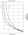
- FIG. 1D is a graphic diagram illustrating a distribution of the group delay ⁇ across multiple transmission frequencies F 1 -F M within a modulation bandwidth of the RF signal 22 in Figure 1A .
- each of the transmission frequencies F 1 -F M is associated with a respective one of multiple variable group delays ⁇ 1 (P IN )- ⁇ M (P IN ), and each of the variable group delays ⁇ 1 (P IN )- ⁇ M (P IN ) varies independently in accordance with the time-variant input power P IN (t).
- FIG. 1E is a graphic diagram illustrating a distribution of the variable phase errors ⁇ ⁇ 1 (P IN )- ⁇ ⁇ M (P IN ) across the transmission frequencies F 1 -F M of the RF signal 22 in Figure 1A .
- each of the transmission frequencies F 1 -F M is associated with a respective one of multiple variable phase errors ⁇ ⁇ 1 (P IN )- ⁇ ⁇ M (P IN ).
- FIG. 1F is a graphic diagram illustrating a distribution of the AM-AM and AM-PM errors across the transmission frequencies F 1 -F M of the RF signal 22 in Figure 1A .
- the AM-PM error ⁇ ERR varies according to the modulated voltage V CC in each of the transmission frequencies F 1 -F M .
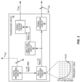
- Figure 2 is a schematic diagram of an example transmission circuit 38 that can be configured according to embodiments of the present disclosure to correct the AM-AM AM ERR and the AM-PM error ⁇ ERR in the existing transmission circuit 10 of Figure 1A across a modulation bandwidth that includes multiple transmission frequencies (a.k.a. target frequencies) F 1 -F M .
- the transmission circuit 38 includes a transceiver circuit 40, a PMIC 42, and a power amplifier circuit 44.
- the transceiver circuit 40 is configured to generate an RF signal 46 in a time-variant input power P IN (t) and for transmission in a selected transmission frequency (a.k.a. selected target frequency) F TGT among the transmission frequencies F 1 -F M .
- the power amplifier circuit 44 is configured to amplify the RF signal 46 from the time-variant input power P IN (t) to a time-variant output power P OUT (t) based on a modulated voltage Vcc to thereby generate an amplified RF signal 46AMP.
- the PMIC 42 is configured to generate the modulated voltage Vcc, which can be an envelope tracking (ET) modulated voltage or an average power tracking (APT) modulated voltage, based on a modulated target voltage V TGT .
- the transceiver circuit 40 is also configured to generate the modulated target voltage V TGT that tracks the time-variant input power P IN (t) and provides the modulated target voltage V TGT to the PMIC 42.
- the modulated target voltage V TGT tracks the time-variant input power P IN (t)
- the modulated voltage Vcc tracks the modulated target voltage V TGT
- the modulated voltage Vcc should be in good alignment with the time-variant input power P lN (t).
- the power amplifier circuit 44 can operate with a linear gain
- the time-variant output power P OUT (t) should also be linearly related to the time-variant input power P lN (t) by the linear gain of the power amplifier circuit 44.
- the power amplifier circuit 44 can also include the output stage 32 (as shown in Figure 1B ) and be coupled to an RF front-end circuit 48 (e.g., a filter, multiplexer, and/or switches).
- the transmission circuit 38 may also suffer the frequency dependent AM-AM error AM ERR and the frequency dependent AM-PM error ⁇ ERR as in the existing transmission circuit 10 of Figure 1A .
- the output reflection coefficient (e.g., S 22 ) of the power amplifier circuit 44 can interact with the input reflection coefficient (e.g., S 11 ) of the RF front-end circuit 48 to create the voltage distortion filter H IV (s) and, consequently, cause the AM-AM error AM ERR and the AM-PM error ⁇ ERR .
- the power amplifier circuit 44 includes a phase shifter 50 and a power amplifier 52.
- the phase shifter 50 is configured to apply a phase shift ⁇ ⁇ to the RF signal 46 to correct the AM-PM error ⁇ ERR . More specifically, the phase shifter 50 is configured to receive a modulated phase correction voltage V ⁇ from the PMIC 42 and determine the phase shift ⁇ ⁇ based on the modulated phase correction voltage V ⁇ .
- the phase shifter 50 may include internal storage (not shown), such as registers for example, to store a correlation between various levels of the modulated phase correction voltage V ⁇ and various degrees of phase shift ⁇ ⁇ .
- the phase shifter 50 can store a correlation between the modulated phase correction voltage V ⁇ of 0 V, 1 V, and 2 V and the phase shift ⁇ ⁇ of 0°, 1°, and 2°, respectively. Accordingly, the phase shifter 50 can determine the correct phase shift ⁇ ⁇ based on the modulated phase correction voltage V ⁇ and apply the determined phase shift ⁇ ⁇ to the RF signal 46 to generate a phase-shifted RF signal 46 ⁇ . Understandably, since the phase shifter 50 only applies the phase shift ⁇ ⁇ to the RF signal 46, the phase-shifted RF signal 46 ⁇ will have the same time-variant input power P IN (t) and in the same selected target frequency F TGT .
- the power amplifier 52 can amplify the phase-shifted RF signal 46 ⁇ based on a modulate voltage, such as an envelope tracking (ET) voltage or an average power tracking (APT) voltage, to generate the amplified RF signal 46AMP. Understandably, since the power amplifier 52 only changes the time-variant input power P IN (t) in the phase-shifted RF signal 46 ⁇ to the time-variant output power P OUT (t) in the amplified RF signal 46AMP, the amplified RF signal 46AMP will maintain the same phase as in the phase-shifted RF signal 46 ⁇ . Thus, by generating the modulated phase correction voltage V ⁇ at a proper voltage level, it is possible to correct the AM-PM error ⁇ ERR in the amplified RF signal 46AMP.
- a modulate voltage such as an envelope tracking (ET) voltage or an average power tracking (APT) voltage
- the transceiver circuit 40 is configured to generate the modulated voltage V TGT and provide the modulated target voltage V TGT to the voltage modulation circuit 54 and the phase correction circuit 56.
- Figure 3 is a schematic diagram illustrating the transceiver circuit 40 configured according to an embodiment of the present disclosure. Common elements between Figures 2 and 3 are shown therein with common element numbers and will not be re-described herein.
- the input vector b MOD can be associated with multiple variable group delays ⁇ 1 (P IN )- ⁇ M (P IN ), each corresponding to a respective one of the transmission frequencies F 1 -F M .
- the variable group delays ⁇ 1 (P IN )- ⁇ M (P IN ) can be different from one another between the transmission frequencies F 1 -F M .
- the delay equalizer circuit 60 is configured to apply a delay equalization filter H ⁇ (s) to the input vector b MOD to convert each of the variable group delays ⁇ 1 (P IN )- ⁇ M (P IN ) into a respective one of multiple constant group delays ⁇ 1 - ⁇ M , as illustrated in Figure 4A.
- Figure 4A is a graphic diagram illustrating a distribution of the constant group delays ⁇ 1 - ⁇ M across the transmission frequencies F 1 -F M as a result of applying the delay equalization filter H ⁇ (s) to the input vector b MOD . As shown in Figure 4A , for each of the transmission frequencies F 1 -F M , the respective one of the group delays ⁇ 1 - ⁇ M stays constant relative to the time-variant input power P IN (t).
- variable phase errors ⁇ ⁇ 1 (P IN )- ⁇ ⁇ M (P IN ) will in turn exhibit a linear relationship across the transmission frequencies F 1 -F M , as illustrated in Figure 4B .
- Figure 4B is a graphic diagram illustrating a distribution of the variable phase errors ⁇ ⁇ 1 (P IN )- ⁇ ⁇ M (P IN ) across the transmission frequencies F 1 -F M as a result of applying the delay equalization filter H ⁇ (s) to the input vector b MOD .
- each of the variable phase errors ⁇ ⁇ 1 (P IN )- ⁇ ⁇ M (P IN ) can be moved up or down based on an appropriate scaling factor F SCALE to superimpose on another one of the variable phase errors ⁇ ⁇ 1 (P IN )- ⁇ ⁇ M (P IN ).
- the delay equalizer circuit 60 by applying the delay equalization filter H ⁇ (s) to the input vector b MOD , the delay equalizer circuit 60 generates a delay-equalized vector b MOD ⁇ ⁇ ⁇ .
- the delay-equalized vector b MOD - ⁇ can be associated with a respective one of the constant group delays ⁇ 1 - ⁇ M corresponding to the selected target frequency F TGT .
- the signal conversion circuit 66 which may include, for example, a digital-to-analog converter (DAC) and a frequency converter, can then convert the delay-equalized vector b MOD - ⁇ in the RF signal 46 in the selected target frequency F TGT .
- the digital processing circuit 58 may be configured to generate an indication 68 that indicates the selected target frequency F TGT and provide the indication 68 to the phase correction circuit 56.
- the amplitude correction circuit 62 is configured to equalize the delay-equalized vector b MOD - ⁇ to thereby generate a delay-gain-equalized vector b MOD ⁇ FG ⁇ having a constant gain in the selected target frequency F TGT .
- the target voltage circuit 64 in turn, generates the modulated target voltage V TGT from the delay-gain-equalized vector b MOD ⁇ ⁇ G ⁇ and provides the modulated target voltage V TGT to the PMIC 42.
- the amplitude correction circuit 62 please refer to U.S. Patent Application Number 17/700,826 , entitled "ENVELOPE TRACKING VOLTAGE CORRECTION IN A TRANSMISSION CIRCUIT.”
- the phase correction circuit 56 is configured to explore the linearity and scalability characteristics of variable phase errors ⁇ ⁇ 1 (P IN )- ⁇ ⁇ M (P IN ) across the transmission frequencies F 1 -F M , as illustrated in Figure 4B , to thereby determine the modulated phase correction voltage V ⁇ .
- the phase correction circuit 56 includes a phase correction voltage lookup table (LUT) circuit 70 and a scaling circuit 72.
- the phase correction voltage LUT circuit 70 may include a phase correction voltage LUT (not shown) that correlates the modulated target voltage V TGT with various levels of a reference phase correction voltage V ⁇ -REF predefined for a reference frequency F REF .
- the reference frequency F REF can be any of the target frequencies F 1 -F M , a center frequency of the modulation bandwidth of the transmission circuit 38, or even an arbitrary frequency. Moreover, the reference frequency F REF may be identical to or different from the selected target frequency F TGT . In this regard, the phase correction voltage LUT circuit 70 can look up the phase correction LUT to select the reference phase correction voltage V ⁇ -REF based on the modulated target voltage V TGT .
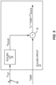
- Figure 5 is a schematic diagram illustrating the scaling circuit 72 in the phase correction circuit 56 in Figure 2 . Common elements between Figures 2 and 5 are shown therein with common element numbers and will not be re-described herein.
- the scaling circuit 72 includes a scaling LUT circuit 74 and a multiplier 76.
- the scaling LUT circuit 74 is configured to determine the scaling factor F SCALE corresponding to the selected target frequency F TGT based on, for example, a scaling LUT (not shown) stored in the scaling LUT circuit 74.
- the transmission circuit 38 of Figure 2 can be configured to correct the AM-AM error AM ERR and the AM-PM error ⁇ ERR based on a process.
- Figure 6 is a flowchart of an example process 200 that can be employed by the transmission circuit of Figure 2 to correct the AM-AM error AM ERR and the AM-PM error ⁇ ERR .
- the phase correction circuit 56 receives the modulated target voltage V TGT and the indication 68 that indicates the selected target frequency F TGT among the target frequencies F 1 -F M (step 202). Accordingly, the phase correction circuit 56 determines the reference phase correction voltage V ⁇ -REF corresponding to a reference frequency F REF based on the modulated target voltage V TGT (step 204). Next, the phase correction circuit 56 determines the scaling factor F SCALE corresponding to the selected target frequency F TGT (step 206). Subsequently, the phase correction circuit 56 generates the phase correction voltage V ⁇ based on the determined reference phase correction voltage V ⁇ -REF and the determined scaling factor F SCALE (step 208).
- the phase shifter 50 determines the phase shift ⁇ ⁇ based on the phase correction voltage V ⁇ (step 210). Accordingly, the phase shifter applies the phase shift ⁇ ⁇ to the RF signal 46, which is modulated for transmission in the selected target frequency F TGT , to thereby generate a phase-shifted RF signal 46 ⁇ (step 212).
- the transmission circuit includes a transceiver circuit, a power management integrated circuit (PMIC), and a power amplifier circuit(s).
- the transceiver circuit generates a radio frequency (RF) signal(s) from an input vector
- the PMIC generates a modulated voltage
- the power amplifier circuit(s) amplifies the RF signal(s) based on the modulated voltage.
- RF radio frequency
- the power amplifier circuit(s) is coupled to an RF front-end circuit, unwanted amplitude-amplitude (AM-AM) and amplitude-phase (AM-PM) errors may be created across a modulation bandwidth of the transmission circuit.
- AM-AM unwanted amplitude-amplitude
- AM-PM amplitude-phase
- the input vector is equalized based on multiple complex filters to thereby cause the AM-AM and AM-PM errors to be corrected in the transmission circuit.
- the input vector is equalized based on multiple complex filters to thereby cause the AM-AM and AM-PM errors to be corrected in the transmission circuit.
Landscapes
- Engineering & Computer Science (AREA)
- Power Engineering (AREA)
- Physics & Mathematics (AREA)
- Nonlinear Science (AREA)
- Computer Networks & Wireless Communication (AREA)
- Signal Processing (AREA)
- Microelectronics & Electronic Packaging (AREA)
- Transmitters (AREA)
Abstract
Description
- This application claims the benefit of provisional patent application serial number
63/245,160, filed September 16, 2021 63/245,151, filed September 16, 2021 - The technology of the disclosure relates generally to correcting amplitude-amplitude (AM-AM) and amplitude-phase (AM-PM) errors in a transmission circuit.
- Mobile communication devices have become increasingly common in current society for providing wireless communication services. The prevalence of these mobile communication devices is driven in part by the many functions that are now enabled on such devices. Increased processing capability in such devices means that mobile communication devices have evolved from being pure communication tools into sophisticated mobile multimedia centers that enable enhanced user experiences.
- The redefined user experience relies on a higher data rate offered by advanced fifth generation (5G) and 5G new radio (5G-NR) technologies, which typically transmit and receive radio frequency (RF) signals in millimeter wave spectrums. Given that the RF signals are more susceptible to attenuation and interference in the millimeter wave spectrums, the RF signals are typically amplified by state-of-the-art power amplifiers to help boost the RF signals to higher power before transmission.
- In a typical transmission circuit, a transceiver circuit is configured to generate an RF signal, a power management circuit is configured to generate a modulated voltage, a power amplifier circuit is configured to amplify the RF signal based on the modulated voltage, and an antenna circuit is configured to transmit the RF signal in one or more transmission frequencies. The power amplifier circuit can be further coupled to the antenna circuit via an RF front-end circuit (e.g., filter, switches, etc.). Notably, an output reflection coefficient (e.g., S22) of the power amplifier circuit can interact with an input reflection coefficient (e.g., S11) of the RF front-end circuit to cause a group delay in the RF signal to potentially create an amplitude-to-amplitude (AM-AM) error in the modulated voltage and/or an amplitude-to-phase (AM-PM) error in the RF signal. As such, it is desirable to correct the AM-AM and AM-PM errors in all of the transmission frequencies to help prevent undesired amplitude distortion and/or spectrum regrowth, particularly when the RF signal is modulated across a wide modulation bandwidth (e.g., ≥ 200 MHz).
- The invention is defined in the appended claims. Embodiments of the disclosure relate to phase and amplitude error correction in a transmission circuit. The transmission circuit includes a transceiver circuit, a power management integrated circuit (PMIC), and a power amplifier circuit(s). The transceiver circuit generates a radio frequency (RF) signal(s) from an input vector, the PMIC generates a modulated voltage, and the power amplifier circuit(s) amplifies the RF signal(s) based on the modulated voltage. When the power amplifier circuit(s) is coupled to an RF front-end circuit (e.g., filter/multiplexer), an output reflection coefficient (e.g., S22) of the power amplifier circuit(s) can interact with an input reflection coefficient (e.g., S11) of the RF front-end circuit to create unwanted amplitude-amplitude (AM-AM) and amplitude-phase (AM-PM) errors across a modulation bandwidth of the transmission circuit. In this regard, in embodiments disclosed herein, the input vector is equalized based on multiple complex filters to thereby cause the AM-AM and AM-PM errors to be corrected in the transmission circuit. As a result, it is possible to reduce undesired instantaneous excessive compression and/or spectrum regrowth across the modulation bandwidth of the transmission circuit.
- In one aspect, a transmission circuit is provided. The transmission circuit includes a PMIC. The PMIC includes a phase correction circuit. The phase correction circuit is configured to receive a modulated target voltage and an indication of a selected target frequency among multiple target frequencies. The phase correction circuit is also configured to determine a reference phase correction voltage corresponding to a reference frequency based on the modulated target voltage. The phase correction circuit is also configured to determine a scaling factor corresponding to the selected target frequency. The phase correction circuit is also configured to generate the phase correction voltage based on the determined reference phase correction voltage and the determined scaling factor. The PMIC also includes a power amplifier circuit. The power amplifier circuit includes a phase shifter. The phase shifter is configured to determine a phase shift based on the phase correction voltage. The phase shifter is also configured to apply the phase shift to an RF signal modulated for transmission in the selected target frequency to thereby generate a phase-shifted RF signal.
- In another aspect, a method for correcting phase and amplitude errors in a transmission circuit is provided. The method includes receiving a modulated target voltage and an indication of a selected target frequency among multiple target frequencies. The method also includes determining a reference phase correction voltage corresponding to a reference frequency based on the modulated target voltage. The method also includes determining a scaling factor corresponding to the selected target frequency. The method also includes generating a phase correction voltage based on the determined reference phase correction voltage and the determined scaling factor. The method also includes determining a phase shift based on the phase correction voltage. The method also includes applying the phase shift to an RF signal modulated for transmission in the selected target frequency to thereby generate a phase-shifted RF signal.
- In another aspect, a PMIC is provided. The PMIC includes a phase correction circuit. The phase correction circuit is configured to receive a modulated target voltage and an indication of a selected target frequency among multiple target frequencies. The phase correction circuit is also configured to determine a reference phase correction voltage corresponding to a reference frequency based on the modulated target voltage. The phase correction circuit is also configured to determine a scaling factor corresponding to the selected target frequency. The phase correction circuit is also configured to generate a phase correction voltage based on the determined reference phase correction voltage and the determined scaling factor. The PMIC also includes a voltage modulation circuit. The voltage modulation circuit is configured to generate a modulated voltage based on the modulated target voltage.
- Those skilled in the art will appreciate the scope of the present disclosure and realize additional aspects thereof after reading the following detailed description of the preferred embodiments in association with the accompanying drawing figures.
- The accompanying drawing figures incorporated in and forming a part of this specification illustrate several aspects of the disclosure, and together with the description serve to explain the principles of the disclosure.
-
Figure 1A is a schematic diagram of an example existing transmission circuit, wherein unwanted amplitude-amplitude (AM-AM) and amplitude-phase (AM-PM) errors may be created when a power amplifier circuit is coupled to a radio frequency (RF) front-end circuit; -
Figure 1B is a schematic diagram providing an example illustration of an output stage of the power amplifier circuit inFigure 1A ; -
Figure 1C is a schematic diagram of an example equivalent model providing an example illustration of the unwanted voltage distortion filter created by a coupling between the power amplifier circuit and the RF front-end circuit 14 inFigure 1A ; -
Figure 1D is a graphic diagram illustrating a distribution of multiple group delays across multiple transmission frequencies; -
Figure 1E is a graphic diagram illustrating a distribution of multiple variable phase errors across multiple transmission frequencies; -
Figure 1F is a graphic diagram illustrating a distribution of the AM-AM and AM-PM errors across multiple transmission frequencies; -
Figure 2 is a schematic diagram of an example transmission circuit that can be configured according to embodiments of the present disclosure to correct the AM-AM and the AM-PM errors across a modulation bandwidth that includes multiple transmission frequencies; -
Figure 3 is a schematic diagram illustrating a transceiver circuit in the transmission circuit ofFigure 2 configured according to an embodiment of the present disclosure; -
Figure 4A is a graphic diagram illustrating a distribution of multiple constant group delays across multiple transmission frequencies; -
Figure 4B is a graphic diagram illustrating a distribution of multiple linearly related variable phase errors across the multiple transmission frequencies inFigure 4A ; -
Figure 5 is a schematic diagram illustrating a scaling circuit in the transmission circuit ofFigure 2 configured according to an embodiment of the present disclosure; and -
Figure 6 is a flowchart of an example process that can be performed by the transmission circuit ofFigure 2 to correct the AM-AM and AM-PM errors in the transmission circuit. - The embodiments set forth below represent the necessary information to enable those skilled in the art to practice the embodiments and illustrate the best mode of practicing the embodiments. Upon reading the following description in light of the accompanying drawing figures, those skilled in the art will understand the concepts of the disclosure and will recognize applications of these concepts not particularly addressed herein. It should be understood that these concepts and applications fall within the scope of the disclosure and the accompanying claims.
- It will be understood that, although the terms first, second, etc. may be used herein to describe various elements, these elements should not be limited by these terms. These terms are only used to distinguish one element from another. For example, a first element could be termed a second element, and, similarly, a second element could be termed a first element, without departing from the scope of the present disclosure. As used herein, the term "and/or" includes any and all combinations of one or more of the associated listed items.
- It will be understood that when an element such as a layer, region, or substrate is referred to as being "on" or extending "onto" another element, it can be directly on or extend directly onto the other element or intervening elements may also be present. In contrast, when an element is referred to as being "directly on" or extending "directly onto" another element, there are no intervening elements present. Likewise, it will be understood that when an element such as a layer, region, or substrate is referred to as being "over" or extending "over" another element, it can be directly over or extend directly over the other element or intervening elements may also be present. In contrast, when an element is referred to as being "directly over" or extending "directly over" another element, there are no intervening elements present. It will also be understood that when an element is referred to as being "connected" or "coupled" to another element, it can be directly connected or coupled to the other element or intervening elements may be present. In contrast, when an element is referred to as being "directly connected" or "directly coupled" to another element, there are no intervening elements present.
- Relative terms such as "below" or "above" or "upper" or "lower" or "horizontal" or "vertical" may be used herein to describe a relationship of one element, layer, or region to another element, layer, or region as illustrated in the Figures. It will be understood that these terms and those discussed above are intended to encompass different orientations of the device in addition to the orientation depicted in the Figures.
- The terminology used herein is for the purpose of describing particular embodiments only and is not intended to be limiting of the disclosure. As used herein, the singular forms "a," "an," and "the" are intended to include the plural forms as well, unless the context clearly indicates otherwise. It will be further understood that the terms "comprises," "comprising," "includes," and/or "including" when used herein specify the presence of stated features, integers, steps, operations, elements, and/or components, but do not preclude the presence or addition of one or more other features, integers, steps, operations, elements, components, and/or groups thereof.
- Unless otherwise defined, all terms (including technical and scientific terms) used herein have the same meaning as commonly understood by one of ordinary skill in the art to which this disclosure belongs. It will be further understood that terms used herein should be interpreted as having a meaning that is consistent with their meaning in the context of this specification and the relevant art and will not be interpreted in an idealized or overly formal sense unless expressly so defined herein.
- Embodiments of the disclosure relate to phase and amplitude error correction in a transmission circuit. The transmission circuit includes a transceiver circuit, a power management integrated circuit (PMIC), and a power amplifier circuit(s). The transceiver circuit generates a radio frequency (RF) signal(s) from an input vector, the PMIC generates a modulated voltage, and the power amplifier circuit(s) amplifies the RF signal(s) based on the modulated voltage. When the power amplifier circuit(s) is coupled to an RF front-end circuit (e.g., filter/multiplexer), an output reflection coefficient (e.g., S22) of the power amplifier circuit(s) can interact with an input reflection coefficient (e.g., S11) of the RF front-end circuit to create unwanted amplitude-amplitude (AM-AM) and amplitude-phase (AM-PM) errors across a modulation bandwidth of the transmission circuit. In this regard, in embodiments disclosed herein, the input vector is equalized based on multiple complex filters to thereby cause the AM-AM and AM-PM errors to be corrected in the transmission circuit. As a result, it is possible to reduce undesired instantaneous excessive compression and/or spectrum regrowth across the modulation bandwidth of the transmission circuit.
- Before discussing the transmission circuit according to the present disclosure, starting at
Figure 2 , a brief discussion of an existing transmission circuit is first provided to help understand how unwanted AM-AM and AM-PM errors may be created when a power amplifier circuit is coupled to an RF front-end circuit, such as a filter/multiplexer circuit. -
Figure 1A is a schematic diagram of an example existingtransmission circuit 10, wherein an unwanted voltage distortion filter HIV(s) may be created on apower amplifier circuit 12 when thepower amplifier circuit 12 is coupled to an RF front-end circuit 14. Notably, in the unwanted voltage distortion filter HIV(s), "s" is a notation of Laplace transform. The existingtransmission circuit 10 includes atransceiver circuit 16, a power management integrated circuit (PMIC) 18, and atransmitter circuit 20, which can include an antenna(s) (not shown) as an example. - The
transceiver circuit 16 is configured to generate anRF signal 22 having a time-variant input power PIN(t) that corresponds to a time-variant voltage envelope 24 and provides theRF signal 22 to thepower amplifier circuit 12. Thetransceiver circuit 16 is also configured to generate a time-variant target voltage VTGT, which is associated with a time-varianttarget voltage envelope 26 that tracks the time-variant voltage envelope 24 of theRF signal 22. ThePMIC 18 is configured to generate a modulated voltage Vcc having a time-variant modulatedvoltage envelope 28 that tracks the time-varianttarget voltage envelope 26 of the time-variant target voltage VTGT and provides the modulated voltage Vcc to thepower amplifier circuit 12. Thepower amplifier circuit 12 is configured to amplify theRF signal 22 based on the modulated voltage Vcc to a time-variant output voltage VOUT associated with a time-variantoutput voltage envelope 30. Thepower amplifier circuit 12 then provides the amplifiedRF signal 22 to the RF front-end circuit 14. The RF front-end circuit 14 may include, for example, a filter circuit that performs further frequency filtering on the amplifiedRF signal 22 before providing the amplifiedRF signal 22 to thetransmitter circuit 20 for transmission. -
Figure 1B is a schematic diagram providing an example illustration of anoutput stage 32 of thepower amplifier circuit 12 inFigure 1A . Common elements betweenFigures 1A and1B are shown therein with common element numbers and will not be re-described herein. - The
output stage 32 can include at least onetransistor 34, such as a bipolar junction transistor (BJT) or a complementary metal-oxide semiconductor (CMOS) transistor. Taking the BJT as an example, thetransistor 34 can include a base electrode B, a collector electrode C, and an emitter electrode E. The base electrode B is configured to receive a bias voltage VBIAS and the collector electrode C is configured to receive the modulated voltage Vcc. The collector electrode C is also coupled to the RF front-end circuit 14 and configured to output the amplifiedRF signal 22 at the output voltage VOUT. In this regard, the output voltage VOUT can be a function of the modulated voltage Vcc. Understandably, thepower amplifier circuit 12 will operate with good efficiency and linearity when the time-variant modulatedvoltage envelope 28 is aligned with the time-variantoutput voltage envelope 30. -
Figure 1C is a schematic diagram of an exampleequivalent model 36 providing an example illustration of the voltage distortion filter HIV(s) created by the coupling between thepower amplifier circuit 12 and the RF front-end circuit 14 in the existingtransmission circuit 10 ofFigure 1A . Common elements betweenFigures 1A-1C are shown therein with common element numbers and will not be re-described herein - In the
equivalent model 36, VPA and ZPA represent theoutput stage 32 of thepower amplifier circuit 12 and an inherent impedance of thepower amplifier circuit 12, respectively, and Z11 represents an inherent impedance associated with an input port of the RF front-end circuit 14. Herein, VOUT represents an output voltage associated with theRF signal 22 before thepower amplifier circuit 12 is coupled to the RF front-end circuit 14, and V'OUT represents an output voltage associated with theRF signal 22 after thepower amplifier circuit 12 is coupled to the RF front-end circuit 14. Hereinafter, the output voltages VOUT and V'OUT are referred to as "non-coupled output voltage" and "coupled output voltage," respectively, for distinction. - A Laplace transform representative of the coupled output voltage V'OUT can be expressed in equation (Eq. 1) below.


- In the equation (Eq. 1) above, T PA(S) represents a reflection coefficient looking back into the
output stage 32 of thepower amplifier circuit 12 and T I(s) represents a reflection coefficient looking into the RF front-end circuit 14. Notably, T PA(S) and T I(s) are complex filters containing amplitude and phase information. In this regard, the T PA(S), the T I(S), and, therefore, the voltage distortion filter HIV(s) are dependents of such factors as modulation bandwidth, RF frequency, and/or voltage standing wave ratio (VSWR). - The equation (Eq. 1) shows that the coupled output voltage V'OUT will be altered from the non-coupled output voltage VOUT by the voltage distortion filter HIV(s) when the
power amplifier circuit 12 is coupled to the RF front-end circuit 14. Moreover, the variation of the non-coupled output voltage VOUT caused by the voltage distortion filter HIV(s) can happen across all frequencies in an entire modulation bandwidth of theRF signal 22. As a result, the coupled output voltage V'OUT may become misaligned from the modulated voltage Vcc across the modulation bandwidth of theRF signal 22, thus causing a frequency dependent AM-AM error AMERR across the modulation bandwidth of the existingtransmission circuit 10. - With reference back to
Figure 1A , when thepower amplifier circuit 12 is coupled to the RF front-end circuit 14, an output reflection coefficient (e.g., S22) of thepower amplifier circuit 12 can interact with an input reflection coefficient (e.g., S11) of the RF front-end circuit 14 to create a group delay τ in theRF signal 22. The group delay τ , which can be expressed in equation (Eq. 2) below, can cause a phase error Δφ at thepower amplifier circuit 12 to thereby create an AM-PM error φ ERR in theRF signal 22.
- Studies have shown that the group delay τ in each of the transmission frequencies varies in accordance with the time-variant input power PIN(t), as illustrated in
Figure 1D. Figure 1D is a graphic diagram illustrating a distribution of the group delay τ across multiple transmission frequencies F1-FM within a modulation bandwidth of theRF signal 22 inFigure 1A . As shown inFigure 1D , each of the transmission frequencies F1-FM is associated with a respective one of multiple variable group delays τ 1(PIN)- τ M(PIN), and each of the variable group delays τ 1(PIN)- τ M(PIN) varies independently in accordance with the time-variant input power PIN(t). - Given the relationship between the group delay τ and the phase error Δφ in equation (Eq. 2), the phase error Δφ associated with each of the variable group delays τ 1(PIN)- τ M(PIN) will also vary according to the time-variant input power PIN(t).
Figure 1E is a graphic diagram illustrating a distribution of the variable phase errors Δφ 1(PIN)-Δφ M(PIN) across the transmission frequencies F1-FM of theRF signal 22 inFigure 1A . As shown inFigure 1E , each of the transmission frequencies F1-FM is associated with a respective one of multiple variable phase errors Δφ 1(PIN)-Δφ M(PIN). Moreover, for any given level of the time-variant input power PIN(t), each of the variable phase errors Δφ 1(PIN)-Δφ M(PIN) associated with a respective one of the transmission frequencies F1-FM is nonlinear relative to any other variable phase errors Δφ 1(PIN)-Δφ M(PIN) associated with any other transmission frequencies F1-FM. For example, the variable phase errors Δφ 1(PIN) associated with the transmission frequency F1 is nonlinearly related to the variable phase errors Δφ M(PIN) associated with the transmission frequency FM for any given value of the time-variant input power PIN(t). - Similar to the frequency dependent amplitude error AMERR, the AM-PM error φ ERR resulted from the variable phase errors Δφ1(PIN)-Δφ M(PIN) are also frequency dependent.
Figure 1F is a graphic diagram illustrating a distribution of the AM-AM and AM-PM errors across the transmission frequencies F1-FM of theRF signal 22 inFigure 1A . - As shown in
Figure 1F , the AM-PM error φ ERR varies according to the modulated voltage VCC in each of the transmission frequencies F1-FM. In this regard, it is necessary to correct both the AM-AM and the AM-PM errors in the existingtransmission circuit 10 to ensure proper alignment between the time-variant voltage envelope 24, the time-variant modulatedvoltage envelope 28, and the time-variantoutput voltage envelope 30. - In this regard,
Figure 2 is a schematic diagram of anexample transmission circuit 38 that can be configured according to embodiments of the present disclosure to correct the AM-AM AMERR and the AM-PM error φ ERR in the existingtransmission circuit 10 ofFigure 1A across a modulation bandwidth that includes multiple transmission frequencies (a.k.a. target frequencies) F1-FM. Herein, thetransmission circuit 38 includes atransceiver circuit 40, aPMIC 42, and apower amplifier circuit 44. - The
transceiver circuit 40 is configured to generate anRF signal 46 in a time-variant input power PIN(t) and for transmission in a selected transmission frequency (a.k.a. selected target frequency) FTGT among the transmission frequencies F1-FM. Thepower amplifier circuit 44 is configured to amplify theRF signal 46 from the time-variant input power PIN(t) to a time-variant output power POUT(t) based on a modulated voltage Vcc to thereby generate an amplified RF signal 46AMP. ThePMIC 42 is configured to generate the modulated voltage Vcc, which can be an envelope tracking (ET) modulated voltage or an average power tracking (APT) modulated voltage, based on a modulated target voltage VTGT. Thetransceiver circuit 40 is also configured to generate the modulated target voltage VTGT that tracks the time-variant input power PIN(t) and provides the modulated target voltage VTGT to thePMIC 42. Ideally, since the modulated target voltage VTGT tracks the time-variant input power PIN(t) and the modulated voltage Vcc tracks the modulated target voltage VTGT, the modulated voltage Vcc should be in good alignment with the time-variant input power PlN(t). In this regard, if thepower amplifier circuit 44 can operate with a linear gain, the time-variant output power POUT(t) should also be linearly related to the time-variant input power PlN(t) by the linear gain of thepower amplifier circuit 44. - Like the
power amplifier circuit 12 inFigure 1A , thepower amplifier circuit 44 can also include the output stage 32 (as shown inFigure 1B ) and be coupled to an RF front-end circuit 48 (e.g., a filter, multiplexer, and/or switches). As such, thetransmission circuit 38 may also suffer the frequency dependent AM-AM error AMERR and the frequency dependent AM-PM error φ ERR as in the existingtransmission circuit 10 ofFigure 1A . In other words, in thetransmission circuit 38, the output reflection coefficient (e.g., S22) of thepower amplifier circuit 44 can interact with the input reflection coefficient (e.g., S11) of the RF front-end circuit 48 to create the voltage distortion filter HIV(s) and, consequently, cause the AM-AM error AMERR and the AM-PM error φ ERR. - As described in detail below, the
transmission circuit 38 can be configured according to various embodiments of the present disclosure to effectively correct the AM-AM error AMERR and the AM-PM error φ ERR. More specifically, thetransmission circuit 38 can concurrently correct the AM-AM and AM-PM errors via multiple complex filters. As a result, thetransmission circuit 38 can reduce undesired instantaneous excessive compression and/or spectrum regrowth to thereby improve efficiency and linearity of thepower amplifier circuit 44 across an entire modulation bandwidth of thetransmission circuit 38. - In an embodiment, the
power amplifier circuit 44 includes aphase shifter 50 and apower amplifier 52. Thephase shifter 50 is configured to apply a phase shift Δφ to theRF signal 46 to correct the AM-PM error φ ERR. More specifically, thephase shifter 50 is configured to receive a modulated phase correction voltage V φ from thePMIC 42 and determine the phase shift Δφ based on the modulated phase correction voltage V φ . In a non-limiting example, thephase shifter 50 may include internal storage (not shown), such as registers for example, to store a correlation between various levels of the modulated phase correction voltage V φ and various degrees of phase shift Δφ. For example, thephase shifter 50 can store a correlation between the modulated phase correction voltage V φ of 0 V, 1 V, and 2 V and the phase shift Δφ of 0°, 1°, and 2°, respectively. Accordingly, thephase shifter 50 can determine the correct phase shift Δφ based on the modulated phase correction voltage V φ and apply the determined phase shift Δφ to theRF signal 46 to generate a phase-shifted RF signal 46φ. Understandably, since thephase shifter 50 only applies the phase shift Δφ to theRF signal 46, the phase-shifted RF signal 46φ will have the same time-variant input power PIN(t) and in the same selected target frequency FTGT. - Subsequently, the
power amplifier 52 can amplify the phase-shifted RF signal 46φ based on a modulate voltage, such as an envelope tracking (ET) voltage or an average power tracking (APT) voltage, to generate the amplified RF signal 46AMP. Understandably, since thepower amplifier 52 only changes the time-variant input power PIN(t) in the phase-shifted RF signal 46φ to the time-variant output power POUT(t) in the amplified RF signal 46AMP, the amplified RF signal 46AMP will maintain the same phase as in the phase-shifted RF signal 46φ. Thus, by generating the modulated phase correction voltage V φ at a proper voltage level, it is possible to correct the AM-PM error φ ERR in the amplified RF signal 46AMP. - The
PMIC 42 includes avoltage modulation circuit 54 and aphase correction circuit 56. According to an embodiment of the present disclosure, thevoltage modulation circuit 54 is configured to generate the modulated voltage Vcc based on the modulated target voltage VTGT and provide the modulated voltage Vcc to thepower amplifier 52. Thephase correction circuit 56 is configured to generate the phase correction voltage V φ based on the modulated target voltage VTGT and provide the phase correction voltage V φ to thephase shifter 50. - In an embodiment, the
transceiver circuit 40 is configured to generate the modulated voltage VTGT and provide the modulated target voltage VTGT to thevoltage modulation circuit 54 and thephase correction circuit 56. In this regard,Figure 3 is a schematic diagram illustrating thetransceiver circuit 40 configured according to an embodiment of the present disclosure. Common elements betweenFigures 2 and3 are shown therein with common element numbers and will not be re-described herein. - Herein, the
transceiver circuit 40 includes adigital processing circuit 58, adelay equalizer circuit 60, anamplitude correction circuit 62, atarget voltage circuit 64, and asignal conversion circuit 66. Thedigital processing circuit 58, which can be a digital baseband circuit as an example, is configured to generate an input vectorbMOD corresponding to a time-variant amplitude AM(t). The input vectorbMOD may be modulated in a baseband frequency that can be converted to any of the transmission frequencies F1-FM within the modulation bandwidth of thetransmission circuit 38. - According to the previous discussion in
Figure 1D , the input vectorbMOD can be associated with multiple variable group delays τ 1(PIN)- τ M(PIN), each corresponding to a respective one of the transmission frequencies F1-FM. In other words, the variable group delays τ 1(PIN)- τ M(PIN) can be different from one another between the transmission frequencies F1-FM. - The
delay equalizer circuit 60 is configured to apply a delay equalization filter H τ (s) to the input vectorbMOD to convert each of the variable group delays τ 1(PIN)- τ M(PIN) into a respective one of multiple constant group delays τ 1- τ M, as illustrated inFigure 4A. Figure 4A is a graphic diagram illustrating a distribution of the constant group delays τ 1- τ M across the transmission frequencies F1-FM as a result of applying the delay equalization filter H τ (s) to the input vectorbMOD . As shown inFigure 4A , for each of the transmission frequencies F1-FM, the respective one of the group delays τ 1- τ M stays constant relative to the time-variant input power PIN(t). - Given the constant group delays τ 1- τ M and the τ-Δφ relationship established in equation (Eq. 2), the variable phase errors Δφ 1(PIN)-Δφ M(PIN) will in turn exhibit a linear relationship across the transmission frequencies F1-FM, as illustrated in
Figure 4B . -
Figure 4B is a graphic diagram illustrating a distribution of the variable phase errors Δφ 1(PIN)-Δφ M(PIN) across the transmission frequencies F1-FM as a result of applying the delay equalization filter H τ (s) to the input vectorbMOD . Given the linear relationship between the variable phase errors Δφ 1(PIN)-Δφ M(PIN), each of the variable phase errors Δφ 1(PIN)-Δφ M(PIN) can be moved up or down based on an appropriate scaling factor FSCALE to superimpose on another one of the variable phase errors Δφ 1(PIN)-Δφ M(PIN). For example, the variable phase errors Δφ 1(PIN) associated with the transmission frequency F1 can be moved downward to superimpose on the variable phase errors Δφ M(PIN) associated with the transmission frequency FM. Likewise, the variable phase errors Δφ M(PIN) associated with the transmission frequency FM can be moved upward to superimpose on the variable phase errors Δφ 1(PIN) associated with the transmission frequency F1. - With reference back to
Figure 3 , by applying the delay equalization filter H τ (s) to the input vectorbMOD , thedelay equalizer circuit 60 generates a delay-equalized vector
bMOD-τ can be associated with a respective one of the constant group delays τ 1- τ M corresponding to the selected target frequency FTGT. Thesignal conversion circuit 66, which may include, for example, a digital-to-analog converter (DAC) and a frequency converter, can then convert the delay-equalized vectorbMOD-τ in theRF signal 46 in the selected target frequency FTGT. In an embodiment, thedigital processing circuit 58 may be configured to generate anindication 68 that indicates the selected target frequency FTGT and provide theindication 68 to thephase correction circuit 56. - To correct the AM-AM error AMERR, the
amplitude correction circuit 62 is configured to equalize the delay-equalized vectorbMOD-τ to thereby generate a delay-gain-equalized vector
target voltage circuit 64, in turn, generates the modulated target voltage VTGT from the delay-gain-equalized vector
PMIC 42. For an in-depth description of theamplitude correction circuit 62, please refer toU.S. Patent Application Number 17/700,826 , entitled "ENVELOPE TRACKING VOLTAGE CORRECTION IN A TRANSMISSION CIRCUIT." - With reference back to
Figure 2 , to correct the AM-PM error φ ERR, thephase correction circuit 56 is configured to explore the linearity and scalability characteristics of variable phase errors Δφ 1(PIN)-Δφ M(PIN) across the transmission frequencies F1-FM, as illustrated inFigure 4B , to thereby determine the modulated phase correction voltage V φ . In an embodiment, thephase correction circuit 56 includes a phase correction voltage lookup table (LUT)circuit 70 and ascaling circuit 72. The phase correctionvoltage LUT circuit 70 may include a phase correction voltage LUT (not shown) that correlates the modulated target voltage VTGT with various levels of a reference phase correction voltage V φ-REF predefined for a reference frequency FREF. In a non-limiting example, the reference frequency FREF can be any of the target frequencies F1-FM, a center frequency of the modulation bandwidth of thetransmission circuit 38, or even an arbitrary frequency. Moreover, the reference frequency FREF may be identical to or different from the selected target frequency FTGT. In this regard, the phase correctionvoltage LUT circuit 70 can look up the phase correction LUT to select the reference phase correction voltage V φ-REF based on the modulated target voltage VTGT. -
Figure 5 is a schematic diagram illustrating the scalingcircuit 72 in thephase correction circuit 56 inFigure 2 . Common elements betweenFigures 2 and5 are shown therein with common element numbers and will not be re-described herein. - In an embodiment, the scaling
circuit 72 includes a scalingLUT circuit 74 and amultiplier 76. The scalingLUT circuit 74 is configured to determine the scaling factor FSCALE corresponding to the selected target frequency FTGT based on, for example, a scaling LUT (not shown) stored in the scalingLUT circuit 74. Themultiplier 76 is configured to multiply the reference phase correction voltage V φ-REF by the scaling factor FSCALE to thereby generate the phase correction voltage V φ (V φ = V φ-REF × FSCALE). - The
transmission circuit 38 ofFigure 2 can be configured to correct the AM-AM error AMERR and the AM-PM error φ ERR based on a process. In this regard,Figure 6 is a flowchart of anexample process 200 that can be employed by the transmission circuit ofFigure 2 to correct the AM-AM error AMERR and the AM-PM error φ ERR. - Herein, the
phase correction circuit 56 receives the modulated target voltage VTGT and theindication 68 that indicates the selected target frequency FTGT among the target frequencies F1-FM (step 202). Accordingly, thephase correction circuit 56 determines the reference phase correction voltage V φ-REF corresponding to a reference frequency FREF based on the modulated target voltage VTGT (step 204). Next, thephase correction circuit 56 determines the scaling factor FSCALE corresponding to the selected target frequency FTGT (step 206). Subsequently, thephase correction circuit 56 generates the phase correction voltage V φ based on the determined reference phase correction voltage V φ-REF and the determined scaling factor FSCALE (step 208). Thephase shifter 50 determines the phase shift Δφ based on the phase correction voltage V φ (step 210). Accordingly, the phase shifter applies the phase shift Δφ to theRF signal 46, which is modulated for transmission in the selected target frequency FTGT, to thereby generate a phase-shifted RF signal 46 φ (step 212). - Thus, from one perspective, phase and amplitude error correction in a transmission circuit is provided. The transmission circuit includes a transceiver circuit, a power management integrated circuit (PMIC), and a power amplifier circuit(s). The transceiver circuit generates a radio frequency (RF) signal(s) from an input vector, the PMIC generates a modulated voltage, and the power amplifier circuit(s) amplifies the RF signal(s) based on the modulated voltage. When the power amplifier circuit(s) is coupled to an RF front-end circuit, unwanted amplitude-amplitude (AM-AM) and amplitude-phase (AM-PM) errors may be created across a modulation bandwidth of the transmission circuit. In this regard, in embodiments disclosed herein, the input vector is equalized based on multiple complex filters to thereby cause the AM-AM and AM-PM errors to be corrected in the transmission circuit. As a result, it is possible to reduce undesired instantaneous excessive compression and/or spectrum regrowth across the modulation bandwidth of the transmission circuit.
- Those skilled in the art will recognize improvements and modifications to the preferred embodiments of the present disclosure. All such improvements and modifications are considered within the scope of the concepts disclosed herein and the claims that follow.
- Further examples of feature combinations taught by the present disclosure are set out in the following numbered clauses:
- 1. A transmission circuit comprising:
- a power management integrated circuit (PMIC) comprising a phase correction circuit configured to:
- receive a modulated target voltage and an indication of a selected target frequency among a plurality of target frequencies;
- determine a reference phase correction voltage corresponding to a reference frequency based on the modulated target voltage;
- determine a scaling factor corresponding to the selected target frequency; and
- generate a phase correction voltage based on the determined reference phase correction voltage and the determined scaling factor; and
- a power amplifier circuit comprising a phase shifter configured to:
- determine a phase shift based on the phase correction voltage; and
- apply the phase shift to a radio frequency (RF) signal modulated for transmission in the selected target frequency to thereby generate a phase-shifted RF signal.
- a power management integrated circuit (PMIC) comprising a phase correction circuit configured to:
- 2. The transmission circuit of clause 1, wherein:
- the power amplifier circuit further comprises a power amplifier configured to amplify the phase-shifted RF signal based on a modulated voltage for transmission in the respective one of the plurality of target frequencies; and
- the PMIC further comprises a voltage modulation circuit configured to generate the modulated voltage based on the modulated target voltage.
- 3. The transmission circuit of clause 1 or clause 2, wherein the phase correction circuit comprises:
- a phase correction voltage lookup table (LUT) circuit configured to determine the reference phase correction voltage corresponding to the reference frequency based on the modulated target voltage; and
- a scaling circuit configured to:
- determine the scaling factor corresponding to the selected target frequency; and
- multiply the reference phase correction voltage by the scaling factor to thereby generate the phase correction voltage.
- 4. The transmission circuit of clause 3, wherein the scaling circuit comprises:
- a scaling LUT circuit configured to determine the scaling factor corresponding to the selected target frequency; and
- a multiplier configured to multiply the reference phase correction voltage by the scaling factor to generate the phase correction voltage.
- 5. The transmission circuit of any preceding clause, wherein the reference frequency is identical to or different from the selected target frequency among the plurality of target frequencies.
- 6. The transmission circuit of any preceding clause, wherein the reference frequency is any one of the plurality of target frequencies.
- 7. The transmission circuit of any preceding clause, further comprising a transceiver circuit configured to:
- generate the RF signal based on an input vector and having a time-variant input power corresponding to a time-variant amplitude of the input vector; and
- generate the modulated target voltage based on the time-variant amplitude of the input vector.
- 8. The transmission circuit of
clause 7, wherein the transceiver circuit comprises:- a digital processing circuit configured to generate the input vector associated with a plurality of time-variant group delays each corresponding to a respective one of the plurality of target frequencies; and
- a delay equalizer circuit configured to:
- equalize the input vector based on a delay equalization filter to thereby convert the plurality of time-variant group delays into a plurality of constant group delays each corresponding to the respective one of the plurality of target frequencies; and
- generate a delay-equalized vector associated with a respective one of the plurality of constant group delays corresponding to the selected target frequency among the plurality of target frequencies; and
- a signal conversion circuit configured to generate the RF signal for transmission in the selected target frequency based on the delay-equalized vector.
- 9. The transmission circuit of clause 8, wherein the digital processing circuit is further configured to generate the indication of the selected target frequency among the plurality of target frequencies.
- 10. The transmission circuit of clause 8 or clause 9, wherein the transceiver circuit further comprises:
- an amplitude correction circuit configured to equalize the delay-equalized vector to thereby generate a delay-gain-equalized vector having a constant gain in the selected target frequency; and
- a target voltage circuit configured to generate the modulated target voltage based on the delay-gain-equalized vector.
- 11. A method for correcting phase and amplitude errors in a transmission circuit comprising:
- receiving a modulated target voltage and an indication of a selected target frequency among a plurality of target frequencies;
- determining a reference phase correction voltage corresponding to a reference frequency based on the modulated target voltage;
- determining a scaling factor corresponding to the selected target frequency;
- generating a phase correction voltage based on the determined reference phase correction voltage and the determined scaling factor;
- determining a phase shift based on the phase correction voltage; and
- applying the phase shift to a radio frequency (RF) signal modulated for transmission in the selected target frequency to thereby generate a phase-shifted RF signal.
- 12. The method of
clause 11, further comprising:- amplifying the phase-shifted RF signal based on a modulated voltage for transmission in the respective one of the plurality of target frequencies; and
- generating the modulated voltage based on the modulated target voltage.
- 13. The method of
clause 11 orclause 12, further comprising:- determining, from a phase correction voltage lookup table (LUT), the reference phase correction voltage corresponding to the reference frequency based on the modulated target voltage; and
- multiplying the reference phase correction voltage by the scaling factor to thereby generate the phase correction voltage.
- 14. The method of any of clauses 11-13, further comprising selecting the reference frequency to be one of:
- identical to the selected target frequency among the plurality of target frequencies; and
- different from the selected target frequency among the plurality of target frequencies.
- 15. The method of any of clauses 11-14, further comprising selecting the reference frequency to be any one of the plurality of target frequencies.
- 16. The method of any of clauses 11-15, further comprising:
- generating the RF signal based on an input vector and having a time-variant input power corresponding to a time-variant amplitude of the input vector; and
- generating the modulated target voltage based on the time-variant amplitude of the input vector.
- 17. The method of
clause 16, further comprising:- generating the input vector associated with a plurality of time-variant group delays each corresponding to a respective one of the plurality of target frequencies;
- equalizing the input vector based on a delay equalization filter to thereby convert the plurality of time-variant group delays into a plurality of constant group delays each corresponding to the respective one of the plurality of target frequencies;
- generating a delay-equalized vector associated with a respective one of the plurality of constant group delays corresponding to the selected target frequency among the plurality of target frequencies; and
- generating the RF signal for transmission in the selected target frequency based on the delay-equalized vector.
- 18. The method of clause 17, further comprising:
- equalizing the delay-equalized vector to thereby generate a delay-gain-equalized vector having a constant gain in the selected target frequency; and
- generating the modulated target voltage based on the delay-gain-equalized vector.
- 19. A power management integrated circuit (PMIC) comprising:
- a phase correction circuit configured to:
- receive a modulated target voltage and an indication of a selected target frequency among a plurality of target frequencies;
- determine a reference phase correction voltage corresponding to a reference frequency based on the modulated target voltage;
- determine a scaling factor corresponding to the selected target frequency; and
- generate a phase correction voltage based on the determined reference phase correction voltage and the determined scaling factor; and
- a voltage modulation circuit configured to generate a modulated voltage based on the modulated target voltage.
- a phase correction circuit configured to:
- 20. The PMIC of clause 19, wherein the phase correction circuit comprises:
- a phase correction voltage lookup table (LUT) circuit configured to determine the reference phase correction voltage corresponding to the reference frequency based on the modulated target voltage; and
- a scaling circuit configured to:
- determine the scaling factor corresponding to the selected target frequency; and
- multiply the reference phase correction voltage by the scaling factor to thereby generate the phase correction voltage.
Claims (15)
- A transmission circuit comprising:a power management integrated circuit (PMIC) comprising a phase correction circuit configured to:receive a modulated target voltage and an indication of a selected target frequency among a plurality of target frequencies;determine a reference phase correction voltage corresponding to a reference frequency based on the modulated target voltage;determine a scaling factor corresponding to the selected target frequency; andgenerate a phase correction voltage based on the determined reference phase correction voltage and the determined scaling factor; anda power amplifier circuit comprising a phase shifter configured to:determine a phase shift based on the phase correction voltage; andapply the phase shift to a radio frequency (RF) signal modulated for transmission in the selected target frequency to thereby generate a phase-shifted RF signal.
- The transmission circuit of claim 1, wherein:the power amplifier circuit further comprises a power amplifier configured to amplify the phase-shifted RF signal based on a modulated voltage for transmission in the respective one of the plurality of target frequencies; andthe PMIC further comprises a voltage modulation circuit configured to generate the modulated voltage based on the modulated target voltage.
- The transmission circuit of claim 1 or claim 2, wherein the phase correction circuit comprises:a phase correction voltage lookup table (LUT) circuit configured to determine the reference phase correction voltage corresponding to the reference frequency based on the modulated target voltage; anda scaling circuit configured to:determine the scaling factor corresponding to the selected target frequency; andmultiply the reference phase correction voltage by the scaling factor to thereby generate the phase correction voltage; andoptionally wherein the scaling circuit comprises:a scaling LUT circuit configured to determine the scaling factor corresponding to the selected target frequency; anda multiplier configured to multiply the reference phase correction voltage by the scaling factor to generate the phase correction voltage.
- The transmission circuit of any preceding claim, wherein the reference frequency is identical to or different from the selected target frequency among the plurality of target frequencies.
- The transmission circuit of any preceding claim, wherein the reference frequency is any one of the plurality of target frequencies.
- The transmission circuit of any preceding claim, further comprising a transceiver circuit configured to:generate the RF signal based on an input vector and having a time-variant input power corresponding to a time-variant amplitude of the input vector; andgenerate the modulated target voltage based on the time-variant amplitude of the input vector.
- The transmission circuit of claim 6, wherein the transceiver circuit comprises:a digital processing circuit configured to generate the input vector associated with a plurality of time-variant group delays each corresponding to a respective one of the plurality of target frequencies; anda delay equalizer circuit configured to:equalize the input vector based on a delay equalization filter to thereby convert the plurality of time-variant group delays into a plurality of constant group delays each corresponding to the respective one of the plurality of target frequencies; andgenerate a delay-equalized vector associated with a respective one of the plurality of constant group delays corresponding to the selected target frequency among the plurality of target frequencies; anda signal conversion circuit configured to generate the RF signal for transmission in the selected target frequency based on the delay-equalized vector; andoptionally wherein:the digital processing circuit is further configured to generate the indication of the selected target frequency among the plurality of target frequencies; and/or the transceiver circuit further comprises:an amplitude correction circuit configured to equalize the delay-equalized vector to thereby generate a delay-gain-equalized vector having a constant gain in the selected target frequency; anda target voltage circuit configured to generate the modulated target voltage based on the delay-gain-equalized vector.
- A method for correcting phase and amplitude errors in a transmission circuit comprising:receiving a modulated target voltage and an indication of a selected target frequency among a plurality of target frequencies;determining a reference phase correction voltage corresponding to a reference frequency based on the modulated target voltage;determining a scaling factor corresponding to the selected target frequency;generating a phase correction voltage based on the determined reference phase correction voltage and the determined scaling factor;determining a phase shift based on the phase correction voltage; andapplying the phase shift to a radio frequency (RF) signal modulated for transmission in the selected target frequency to thereby generate a phase-shifted RF signal.
- The method of claim 8, further comprising:amplifying the phase-shifted RF signal based on a modulated voltage for transmission in the respective one of the plurality of target frequencies; andgenerating the modulated voltage based on the modulated target voltage.
- The method of claim 8 or claim 9, further comprising:determining, from a phase correction voltage lookup table (LUT), the reference phase correction voltage corresponding to the reference frequency based on the modulated target voltage; andmultiplying the reference phase correction voltage by the scaling factor to thereby generate the phase correction voltage.
- The method of any of claims 8-10, further comprising selecting the reference frequency to be one of:identical to the selected target frequency among the plurality of target frequencies; anddifferent from the selected target frequency among the plurality of target frequencies.
- The method of any of claims 8-11, further comprising selecting the reference frequency to be any one of the plurality of target frequencies.
- The method of any of claims 8-12, further comprising:generating the RF signal based on an input vector and having a time-variant input power corresponding to a time-variant amplitude of the input vector; andgenerating the modulated target voltage based on the time-variant amplitude of the input vector; optionally further comprising:generating the input vector associated with a plurality of time-variant group delays each corresponding to a respective one of the plurality of target frequencies;equalizing the input vector based on a delay equalization filter to thereby convert the plurality of time-variant group delays into a plurality of constant group delays each corresponding to the respective one of the plurality of target frequencies;generating a delay-equalized vector associated with a respective one of the plurality of constant group delays corresponding to the selected target frequency among the plurality of target frequencies; andgenerating the RF signal for transmission in the selected target frequency based on the delay-equalized vector; and further optionally comprising:equalizing the delay-equalized vector to thereby generate a delay-gain-equalized vector having a constant gain in the selected target frequency; andgenerating the modulated target voltage based on the delay-gain-equalized vector.
- A power management integrated circuit (PMIC) comprising:a phase correction circuit configured to:receive a modulated target voltage and an indication of a selected target frequency among a plurality of target frequencies;determine a reference phase correction voltage corresponding to a reference frequency based on the modulated target voltage;determine a scaling factor corresponding to the selected target frequency; andgenerate a phase correction voltage based on the determined reference phase correction voltage and the determined scaling factor; anda voltage modulation circuit configured to generate a modulated voltage based on the modulated target voltage.
- The PMIC of claim 14, wherein the phase correction circuit comprises:a phase correction voltage lookup table (LUT) circuit configured to determine the reference phase correction voltage corresponding to the reference frequency based on the modulated target voltage; anda scaling circuit configured to:determine the scaling factor corresponding to the selected target frequency; andmultiply the reference phase correction voltage by the scaling factor to thereby generate the phase correction voltage.
Applications Claiming Priority (3)
| Application Number | Priority Date | Filing Date | Title |
|---|---|---|---|
| US202163245151P | 2021-09-16 | 2021-09-16 | |
| US202163245160P | 2021-09-16 | 2021-09-16 | |
| US17/939,372 US12401332B2 (en) | 2021-09-16 | 2022-09-07 | Phase and amplitude error correction in a transmission circuit |
Publications (1)
| Publication Number | Publication Date |
|---|---|
| EP4152608A1 true EP4152608A1 (en) | 2023-03-22 |
Family
ID=83361139
Family Applications (1)
| Application Number | Title | Priority Date | Filing Date |
|---|---|---|---|
| EP22196188.1A Pending EP4152608A1 (en) | 2021-09-16 | 2022-09-16 | Phase and amplitude error correction in a transmission circuit |
Country Status (4)
| Country | Link |
|---|---|
| US (1) | US12401332B2 (en) |
| EP (1) | EP4152608A1 (en) |
| KR (1) | KR20230040926A (en) |
| CN (1) | CN115865226A (en) |
Citations (3)
| Publication number | Priority date | Publication date | Assignee | Title |
|---|---|---|---|---|
| US20060209881A1 (en) * | 2002-10-18 | 2006-09-21 | Ipwireless, Inc. | Pre-equalisation for umts base station |
| US20140084996A1 (en) * | 2012-09-24 | 2014-03-27 | Motorola Mobility Llc | Method and apparatus for controlling or managing bandwidth of a filter circuit within a system having two integrated circuits |
| CN105812073A (en) * | 2014-12-31 | 2016-07-27 | 上海贝尔股份有限公司 | Horizontal and vertical combined calibration method and device for active antenna array |
Family Cites Families (190)
| Publication number | Priority date | Publication date | Assignee | Title |
|---|---|---|---|---|
| US4797898A (en) | 1986-11-21 | 1989-01-10 | Racal Data Communications Inc. | Method and apparatus for equalization of data transmission system |
| US6760451B1 (en) | 1993-08-03 | 2004-07-06 | Peter Graham Craven | Compensating filters |
| WO1995032561A1 (en) | 1994-05-19 | 1995-11-30 | Ortel Corporation | In-line predistorter for linearization of electronic and optical signals |
| US5793821A (en) | 1995-06-07 | 1998-08-11 | 3Com Corporation | Timing Recovery using group delay compensation |
| US6275685B1 (en) | 1998-12-10 | 2001-08-14 | Nortel Networks Limited | Linear amplifier arrangement |
| US6166601A (en) | 1999-01-07 | 2000-12-26 | Wiseband Communications Ltd. | Super-linear multi-carrier power amplifier |
| EP1104093A1 (en) | 1999-11-24 | 2001-05-30 | Telefonaktiebolaget Lm Ericsson | Method and apparatus for generation of a RF signal |
| CA2329100A1 (en) | 1999-12-21 | 2001-06-21 | Nortel Networks Limited | Phase and amplitude detector and method of determining errors |
| US6570444B2 (en) | 2000-01-26 | 2003-05-27 | Pmc-Sierra, Inc. | Low noise wideband digital predistortion amplifier |
| DE60005223T2 (en) | 2000-02-24 | 2004-07-15 | Fraunhofer-Gesellschaft zur Förderung der angewandten Forschung e.V. | DEVICE FOR PRE-DISTORMING AN INPUT SIGNAL FOR A POWER AMPLIFIER USING NON-ORTHOGONAL COORDINATES |
| US7076225B2 (en) | 2001-02-16 | 2006-07-11 | Qualcomm Incorporated | Variable gain selection in direct conversion receiver |
| US6646519B2 (en) | 2001-05-07 | 2003-11-11 | Viewsonics, Inc. | RF equalizer |
| US6856215B2 (en) | 2001-08-24 | 2005-02-15 | Powerwave Technologies, Inc. | System and method for adjusting group delay |
| US7049907B2 (en) | 2001-08-24 | 2006-05-23 | Powerwave Technologies, Inc. | System and method for adjusting group delay |
| SE0102885D0 (en) | 2001-08-28 | 2001-08-28 | Ericsson Telefon Ab L M | Calibration of an adaptive signal conditioning systern |
| US6806767B2 (en) | 2002-07-09 | 2004-10-19 | Anadigics, Inc. | Power amplifier with load switching circuit |
| ATE451795T1 (en) | 2002-07-10 | 2009-12-15 | Nxp Bv | STEREO SIGNAL PROCESSING DEVICE |
| US7332961B2 (en) | 2002-10-22 | 2008-02-19 | Nxp B.V. | Predistortion linearizing |
| US7583754B2 (en) | 2002-10-31 | 2009-09-01 | Zte Corporation | Method and system for broadband predistortion linearization |
| CN1255938C (en) | 2002-12-10 | 2006-05-10 | 株式会社Ntt都科摩 | Linear power amplifying method and linear power amplifier |
| GB2398648B (en) * | 2003-02-19 | 2005-11-09 | Nujira Ltd | Power supply stage for an amplifier |
| US7397863B2 (en) * | 2003-09-30 | 2008-07-08 | Broadcom Corporation | Implementation technique for linear phase equalization in multi-mode RF transmitters |
| US7522658B2 (en) | 2003-09-30 | 2009-04-21 | Broadcom Corporation | Design method and implementation of optimal linear IIR equalizers for RF transceivers |
| US7430248B2 (en) | 2004-01-27 | 2008-09-30 | Crestcom, Inc. | Predistortion circuit and method for compensating nonlinear distortion in a digital RF communications transmitter |
| SE0402289D0 (en) | 2004-09-21 | 2004-09-21 | Ericsson Telefon Ab L M | predistorter |
| US7336723B2 (en) | 2004-11-08 | 2008-02-26 | Photron Research And Development Pte Ltd. | Systems and methods for high-efficiency transmission of information through narrowband channels |
| WO2006087864A1 (en) | 2005-02-17 | 2006-08-24 | Hitachi Kokusai Electric Inc. | Predistorter |
| US7193462B2 (en) | 2005-03-22 | 2007-03-20 | Powerwave Technologies, Inc. | RF power amplifier system employing an analog predistortion module using zero crossings |
| JP5301831B2 (en) | 2005-06-30 | 2013-09-25 | 富士通株式会社 | Power amplifier having distortion compensation circuit |
| KR101002893B1 (en) | 2005-08-06 | 2010-12-21 | 삼성전자주식회사 | Multimode Power Amplification Method and Apparatus Using Predistorter |
| CN101258690A (en) | 2005-09-06 | 2008-09-03 | 三菱电机株式会社 | Leakage Signal Cancellation Device |
| US7889820B2 (en) | 2006-01-05 | 2011-02-15 | Qualcomm Incorporated | Phase compensation for analog gain switching in OFDM modulated physical channel |
| US7933570B2 (en) | 2006-02-03 | 2011-04-26 | Quantance, Inc. | Power amplifier controller circuit |
| CN100492921C (en) | 2006-05-30 | 2009-05-27 | 华为技术有限公司 | Receiver and method for receiving radio signal |
| US7471204B2 (en) | 2006-07-07 | 2008-12-30 | Broadcom Corporation | Receiver architecture for canceling blocking signals |
| US7945208B2 (en) * | 2006-08-14 | 2011-05-17 | Gct Semiconductor, Inc. | Radio frequency integrated circuit |
| US7830220B2 (en) | 2006-09-26 | 2010-11-09 | Infineon Technologies Ag | Modulator arrangement and method for signal modulation |
| KR20100014339A (en) | 2006-12-26 | 2010-02-10 | 달리 시스템즈 씨오. 엘티디. | Method and system for baseband predistortion linearization in multi-channel wideband communication systems |
| US8400338B2 (en) | 2006-12-29 | 2013-03-19 | Teradyne, Inc. | Compensating for harmonic distortion in an instrument channel |
| US20120244824A1 (en) | 2007-02-12 | 2012-09-27 | Texas Instruments Incorporated | Minimization of rms phase error in a phase locked loop by dithering of a frequency reference |
| US7755429B2 (en) | 2007-02-16 | 2010-07-13 | Microelectronics Technology Inc. | System and method for dynamic drain voltage adjustment to control linearity, output power, and efficiency in RF power amplifiers |
| US7688157B2 (en) | 2007-04-05 | 2010-03-30 | Panasonic Corporation | Selective envelope modulation enabling reduced current consumption |
| US20090004981A1 (en) | 2007-06-27 | 2009-01-01 | Texas Instruments Incorporated | High efficiency digital transmitter incorporating switching power supply and linear power amplifier |
| US7859338B2 (en) | 2007-07-26 | 2010-12-28 | Broadcom Corporation | Compact low-power class AB amplifier |
| US20090061787A1 (en) | 2007-08-30 | 2009-03-05 | Rainer Koller | Transceiver, rf-transceiver, communication system and method for transferring control packets |
| US8059748B2 (en) | 2007-09-19 | 2011-11-15 | Qualcomm, Incorporated | Multi-mode and multi-band transmitters for wireless communication |
| US7739063B2 (en) | 2007-11-14 | 2010-06-15 | Agilent Technologies, Inc. | Nonlinear measurement system error correction |
| FI20075958A0 (en) | 2007-12-21 | 2007-12-21 | Nokia Corp | Processing of broadcast signals in a radio transmitter |
| US9705477B2 (en) | 2008-04-30 | 2017-07-11 | Innovation Digital, LLC | Compensator for removing nonlinear distortion |
| CA2668264A1 (en) | 2008-06-05 | 2009-12-05 | Raytheon Canada Limited | Linearizing technique for power amplifiers |
| US8374282B2 (en) | 2008-07-24 | 2013-02-12 | Motorola Mobility Llc | Method and apparatus for improving digital predistortion correction with amplifier device biasing |
| US8184751B2 (en) | 2008-12-03 | 2012-05-22 | Bae Systems Information And Electronic Systems Integration Inc. | Integrated interference cancellation system architecture with distortion correction |
| EP2252003A1 (en) | 2009-05-12 | 2010-11-17 | CoreOptics Inc. | Phase detection method and phase detector |
| US8385854B2 (en) * | 2009-05-21 | 2013-02-26 | Qualcomm Incorporated | Adaptive parametric power amplifier protection circuit |
| US7978009B2 (en) | 2009-08-03 | 2011-07-12 | Telefonaktiebolaget Lm Ericsson (Publ) | Digital modulated RF power amplifier with impedance compensation circuit |
| CN101651459B (en) | 2009-09-15 | 2013-02-13 | 电子科技大学 | High-efficiency linear LINC transmitter |
| KR101087629B1 (en) | 2009-12-30 | 2011-11-30 | 광주과학기술원 | Multi-Band Power Amplifiers |
| JPWO2011086752A1 (en) | 2010-01-14 | 2013-05-16 | 住友電気工業株式会社 | Amplifying device and signal processing device |
| JP5487996B2 (en) | 2010-01-25 | 2014-05-14 | 富士通株式会社 | Adaptive equalizer and adaptive equalization method |
| JP2011188123A (en) | 2010-03-05 | 2011-09-22 | Panasonic Corp | Transmitter circuit using polar modulation method, and communication device |
| JP2011211533A (en) | 2010-03-30 | 2011-10-20 | Sumitomo Electric Ind Ltd | Amplifier circuit and radio communication apparatus |
| WO2011133542A1 (en) | 2010-04-19 | 2011-10-27 | Rf Micro Devices, Inc. | Pseudo-envelope following power management system |
| US8831544B2 (en) | 2010-04-20 | 2014-09-09 | Rf Micro Devices, Inc. | Dynamic device switching (DDS) of an in-phase RF PA stage and a quadrature-phase RF PA stage |
| JP5402817B2 (en) | 2010-04-30 | 2014-01-29 | 富士通株式会社 | Power amplifier memory effect canceller, wireless transmitter |
| GB2480687B (en) | 2010-05-28 | 2018-04-04 | Snaptrack Inc | Power supply pre-distortion |
| US8749309B2 (en) * | 2010-12-05 | 2014-06-10 | Rf Micro Devices (Cayman Islands), Ltd. | Gate-based output power level control power amplifier |
| US8975960B2 (en) | 2011-02-01 | 2015-03-10 | Mediatek Singapore Pte. Ltd. | Integrated circuit wireless communication unit and method for providing a power supply |
| WO2012151594A2 (en) * | 2011-05-05 | 2012-11-08 | Rf Micro Devices, Inc. | Power managent system for pseudo-envelope and average power tracking |
| US9379667B2 (en) | 2011-05-05 | 2016-06-28 | Rf Micro Devices, Inc. | Multiple power supply input parallel amplifier based envelope tracking |
| US10623014B2 (en) | 2011-06-27 | 2020-04-14 | Syntropy Systems, Llc | Apparatuses and methods for sample rate conversion |
| US10263628B2 (en) | 2011-06-27 | 2019-04-16 | Syntropy Systems, Llc | Apparatuses and methods for converting fluctuations in periodicity of an input signal into fluctuations in amplitude of an output signal |
| KR101784885B1 (en) | 2011-10-14 | 2017-10-13 | 삼성전자주식회사 | Apparatus and method apparatus for interleaving switching in power amplifier |
| US9065504B2 (en) | 2011-10-28 | 2015-06-23 | Broadcom Corporation | Transmitter front end with programmable notch filter and methods for use therewith |
| US9041364B2 (en) | 2011-12-01 | 2015-05-26 | Rf Micro Devices, Inc. | RF power converter |
| US8649745B2 (en) | 2011-12-21 | 2014-02-11 | Telefonaktiebolaget L M Ericsson (Publ) | Adaptive predistortion for a non-linear subsystem based on a model as a concatenation of a non-linear model followed by a linear model |
| US9001947B2 (en) | 2012-01-10 | 2015-04-07 | Telefonaktiebolaget L M Ericsson (Publ) | Linearization of multi-antenna receivers with RF pre-distortion |
| US8952753B2 (en) | 2012-02-17 | 2015-02-10 | Quantance, Inc. | Dynamic power supply employing a linear driver and a switching regulator |
| JP5591853B2 (en) | 2012-03-19 | 2014-09-17 | 株式会社東芝 | Quadrature error compensation circuit |
| CN107612663B (en) | 2012-05-10 | 2021-01-29 | 瑞典爱立信有限公司 | Method and apparatus for hybrid automatic repeat request signaling for carrier aggregation |
| US9225296B2 (en) | 2012-07-23 | 2015-12-29 | Dali Systems Co. Ltd. | Method and system for aligning signals widely spaced in frequency for wideband digital predistortion in wireless communication systems |
| US20140029683A1 (en) | 2012-07-26 | 2014-01-30 | Telefonaktiebolaget L M Ericsson (Publ) | Multi-Band Observation Receiver |
| US9020451B2 (en) | 2012-07-26 | 2015-04-28 | Rf Micro Devices, Inc. | Programmable RF notch filter for envelope tracking |
| US9276475B2 (en) | 2012-08-10 | 2016-03-01 | Texas Instruments Incorporated | Switched mode assisted linear regulator with decoupled output impedance and signal path bandwidth |
| JP6315834B2 (en) | 2012-08-10 | 2018-04-25 | 日本テキサス・インスツルメンツ株式会社 | Switched mode assist linear regulator |
| JP2014045371A (en) | 2012-08-27 | 2014-03-13 | Fujitsu Ltd | Power amplification device |
| US8824980B2 (en) * | 2012-09-05 | 2014-09-02 | Analog Devices, Inc. | System and method to implement a radio transmitter with digital predistortion having reduced noise |
| US8952795B2 (en) | 2012-09-06 | 2015-02-10 | OmniVision Technologies | Selective gain control circuit |
| US9300407B2 (en) | 2012-09-07 | 2016-03-29 | Futurewei Technologies, Inc. | Channel estimation for optical orthogonal frequency division multiplexing systems |
| US8934856B2 (en) | 2012-10-12 | 2015-01-13 | Analog Devices, Inc. | System and method to calibrate the frequency response of an electronic filter |
| US9560595B2 (en) | 2012-12-03 | 2017-01-31 | Broadcom Corporation | Dynamic operating bandwidth configuration for an envelope tracker |
| US9287829B2 (en) | 2012-12-28 | 2016-03-15 | Peregrine Semiconductor Corporation | Control systems and methods for power amplifiers operating in envelope tracking mode |
| US8824981B2 (en) | 2013-01-31 | 2014-09-02 | Intel Mobile Communications GmbH | Recalibration of envelope tracking transfer function during active transmission |
| US9391565B2 (en) | 2013-03-15 | 2016-07-12 | TriQuint International PTE, Ltd. | Amplifier phase distortion correction based on amplitude distortion measurement |
| JP6107358B2 (en) | 2013-04-17 | 2017-04-05 | 富士通株式会社 | Power supply circuit, power supply IC, power amplification device, and wireless communication device |
| US9036734B1 (en) | 2013-07-22 | 2015-05-19 | Altera Corporation | Methods and apparatus for performing digital predistortion using time domain and frequency domain alignment |
| US9197168B2 (en) | 2013-07-23 | 2015-11-24 | Mstar Semiconductor, Inc. | Amplitude modulation to phase modulation (AMPM) distortion compensation |
| US9124315B2 (en) | 2013-11-05 | 2015-09-01 | At&T Mobility Ii Llc | Compressed amplitude wireless signal and compression function |
| JP2015099972A (en) | 2013-11-18 | 2015-05-28 | 三菱電機株式会社 | Transmitter module |
| US9438196B2 (en) | 2014-02-14 | 2016-09-06 | Peregrine Semiconductor Corporation | Integrated tunable filter architecture |
| US10333474B2 (en) | 2014-05-19 | 2019-06-25 | Skyworks Solutions, Inc. | RF transceiver front end module with improved linearity |
| US9692366B2 (en) | 2014-12-09 | 2017-06-27 | Intel Corporation | Envelope tracking path delay fine tuning and calibration |
| US9425742B2 (en) | 2014-12-10 | 2016-08-23 | Intel Corporation | Method and apparatus for correcting inconvenient power amplifier load characteristics in an envelope tracking based system |
| US9930725B2 (en) | 2014-12-16 | 2018-03-27 | Apple Inc. | Wireless electronic device with multiradio controller integrated circuit |
| DE102014119625A1 (en) | 2014-12-23 | 2016-06-23 | Intel IP Corporation | Circuit and method for providing a radio frequency signal |
| US20160182099A1 (en) | 2014-12-23 | 2016-06-23 | Honeywell International Inc. | Systems and methods for efficient multi-channel satcom with dynamic power supply and digital pre-distortion |
| JP6565288B2 (en) | 2015-04-10 | 2019-08-28 | 富士通株式会社 | Wireless device |
| JP2016213603A (en) | 2015-05-01 | 2016-12-15 | 富士通株式会社 | Wireless communication device |
| US9800274B2 (en) | 2015-07-03 | 2017-10-24 | Mediatek, Inc. | Communication units and methods for power supply control |
| US9660675B2 (en) | 2015-10-13 | 2017-05-23 | Analog Devices Global | Digital predistortion and uptilt and cable communication |
| US9673847B1 (en) | 2015-11-25 | 2017-06-06 | Analog Devices, Inc. | Apparatus and methods for transceiver calibration |
| US10716080B2 (en) | 2016-02-09 | 2020-07-14 | Apple Inc. | Calibration techniques for envelope tracking power amplifiers |
| EP3427417B1 (en) | 2016-03-07 | 2022-05-11 | Satixfy UK Limited | Calibration techniques for an antenna array |
| US10033413B2 (en) | 2016-05-19 | 2018-07-24 | Analog Devices Global | Mixed-mode digital predistortion |
| EP3252949B1 (en) | 2016-06-01 | 2020-03-18 | Intel IP Corporation | Methods and devices for predistortion of signals |
| JP6446501B2 (en) | 2016-06-07 | 2018-12-26 | メレクシス・テクノロジーズ・ソシエテ・アノニムMelexis Technologies Sa | Drive circuit for passive resonant circuit and transmitter device |
| US10097138B2 (en) | 2016-07-26 | 2018-10-09 | Nxp Usa, Inc. | Doherty input power splitter and linearization method |
| GB2598210B (en) * | 2016-08-31 | 2022-09-21 | Skyworks Solutions Inc | Multi-input amplifier with degeneration switching block and low loss bypass function |
| US10333479B2 (en) | 2016-12-16 | 2019-06-25 | Qorvo Us, Inc. | Power amplifier with improved linearity |
| JP6680235B2 (en) | 2017-02-09 | 2020-04-15 | 株式会社村田製作所 | Power amplifier circuit and high frequency module |
| US11223376B2 (en) | 2017-02-27 | 2022-01-11 | Apple Inc. | Frequency dependent envelope tracking |
| US9973370B1 (en) | 2017-06-06 | 2018-05-15 | Intel IP Corporation | Memory predistortion in bandwidth limited envelope tracking |
| JP6448881B1 (en) | 2017-06-29 | 2019-01-09 | 三菱電機株式会社 | Distortion compensation device |
| TWI639299B (en) | 2017-08-02 | 2018-10-21 | 立積電子股份有限公司 | Current compensation circuit |
| CN107483021B (en) | 2017-08-15 | 2020-09-08 | 广州联星科技有限公司 | Linear correction circuit, correction method and device for analog predistortion power amplifier |
| US10326490B2 (en) | 2017-08-31 | 2019-06-18 | Qorvo Us, Inc. | Multi radio access technology power management circuit |
| US10778345B2 (en) | 2017-09-11 | 2020-09-15 | Apple, Inc. | Dynamic look up table measurements for transmitter with envelope tracking systems |
| US10326408B2 (en) | 2017-09-18 | 2019-06-18 | Qorvo Us, Inc. | Envelope tracking power management circuit |
| US20190097671A1 (en) | 2017-09-26 | 2019-03-28 | Apple Inc. | Converged transmitter architecture with reduced power consumption |
| US10432145B2 (en) * | 2018-01-15 | 2019-10-01 | Qorvo Us, Inc. | Envelope tracking circuit |
| US10230340B1 (en) | 2018-02-06 | 2019-03-12 | Qorvo Us, Inc. | Wide modulation bandwidth radio frequency circuit |
| US11424718B2 (en) | 2018-03-01 | 2022-08-23 | Telefonaktiebolaget Lm Ericsson (Publ) | Envelope tracking supply modulator for power amplifier |
| US10361744B1 (en) | 2018-03-05 | 2019-07-23 | Qorvo Us, Inc. | Transceiver circuit and related radio frequency circuit |
| US10476437B2 (en) | 2018-03-15 | 2019-11-12 | Qorvo Us, Inc. | Multimode voltage tracker circuit |
| US10764078B2 (en) | 2018-03-23 | 2020-09-01 | Maxlinear, Inc. | Digital predistortion for a frequency-selective channel |
| US10454423B1 (en) | 2018-04-12 | 2019-10-22 | Apple Inc. | Techniques for improving cellular current consumption |
| US10686407B2 (en) | 2018-04-30 | 2020-06-16 | Samsung Electronics Co., Ltd. | Symbol power tracking amplification system and a wireless communication device including the same |
| US10305435B1 (en) | 2018-05-03 | 2019-05-28 | Nokia Solutions And Networks Oy | Transceivers and systems having digital distortion compensation and methods thereof |
| US10833637B2 (en) | 2018-05-21 | 2020-11-10 | Qorvo Us, Inc. | Charge-pump tracker circuitry |
| KR102616755B1 (en) | 2018-09-19 | 2023-12-20 | 인텔 코포레이션 | Ultra-high data rate digital millimeter-wave transmitter with energy-efficient spectral filtering |
| US10911001B2 (en) | 2018-10-02 | 2021-02-02 | Qorvo Us, Inc. | Envelope tracking amplifier circuit |
| JP7302160B2 (en) | 2018-10-29 | 2023-07-04 | 富士通株式会社 | Amplifier circuit and antenna device |
| US10938351B2 (en) * | 2018-10-31 | 2021-03-02 | Qorvo Us, Inc. | Envelope tracking system |
| US11038471B2 (en) | 2018-11-20 | 2021-06-15 | Skyworks Solutions, Inc. | Envelope tracking system with modeling of a power amplifier supply voltage filter |
| US11108610B2 (en) | 2018-12-20 | 2021-08-31 | Qorvo Us, Inc. | Multi-level voltage circuit and related apparatus |
| US11088660B2 (en) | 2019-01-25 | 2021-08-10 | Mediatek Inc. | Power supply with envelope tracking modulation |
| US11025458B2 (en) | 2019-02-07 | 2021-06-01 | Qorvo Us, Inc. | Adaptive frequency equalizer for wide modulation bandwidth envelope tracking |
| US10938350B2 (en) | 2019-03-13 | 2021-03-02 | Qorvo Us, Inc. | Multi-mode envelope tracking target voltage circuit and related apparatus |
| US11424719B2 (en) | 2019-04-18 | 2022-08-23 | Qorvo Us, Inc. | Multi-bandwidth envelope tracking integrated circuit |
| US11387789B2 (en) | 2019-06-05 | 2022-07-12 | Qorvo Us, Inc. | Charge pump tracker circuitry |
| US11637531B1 (en) | 2019-09-05 | 2023-04-25 | Murata Manufacturing Co., Ltd. | Supply generator and associated control methods |
| CN110855251B (en) | 2019-09-09 | 2023-04-11 | 宁波大学 | Single-path serial-type analog predistortion system |
| US11005368B2 (en) | 2019-09-17 | 2021-05-11 | Qualcomm Incorporated | Hysteretic window adjustment of tri-level switching regulator |
| US11223325B2 (en) | 2019-09-27 | 2022-01-11 | Skyworks Solutions, Inc. | Multi-level envelope tracking systems with adjusted voltage steps |
| US11239800B2 (en) | 2019-09-27 | 2022-02-01 | Skyworks Solutions, Inc. | Power amplifier bias modulation for low bandwidth envelope tracking |
| CN110798155A (en) | 2019-10-29 | 2020-02-14 | 电子科技大学 | A power amplifier AM-PM distortion correction circuit and method |
| CN210693998U (en) | 2019-11-04 | 2020-06-05 | 京信通信系统(中国)有限公司 | Analog predistortion processing circuit and signal processing apparatus |
| US20210058970A1 (en) * | 2019-11-08 | 2021-02-25 | Intel Corporation | Mechanisms to operate on a downlink wideband carrier in unlicensed band |
| CN112995079B (en) | 2019-12-13 | 2022-03-11 | 华为技术有限公司 | A signal processing method and related equipment |
| US11271599B2 (en) | 2019-12-19 | 2022-03-08 | Qualcomm Incorporated | Envelope tracking system having fast transition time for a radio frequency (RF) amplifier |
| CN111064438B (en) | 2019-12-25 | 2023-12-08 | 北京普能微电子科技有限公司 | Analog predistortion circuit, power amplifier and radio frequency module |
| US12010053B2 (en) * | 2020-02-13 | 2024-06-11 | Intel Corporation | Transport block size (TBS) determination for sidelink communication |
| US11784861B2 (en) * | 2020-02-13 | 2023-10-10 | Intel Corporation | Channel access related enhancements to New Radio Unlicensed (NR-U) |
| US11545945B2 (en) | 2020-03-04 | 2023-01-03 | Qorvo Us, Inc. | Apparatus and method for calibrating an envelope tracking lookup table |
| WO2021194397A1 (en) | 2020-03-23 | 2021-09-30 | Telefonaktiebolaget Lm Ericsson (Publ) | Amplifier circuits and methods of operating an amplifier circuit |
| CN115668761B (en) | 2020-04-07 | 2026-03-17 | 诺基亚技术有限公司 | Parameter estimation for linearization of nonlinear components |
| US11316482B2 (en) | 2020-06-18 | 2022-04-26 | Silicon Laboratories Inc. | Radio frequency power amplifier adaptive digital pre-distortion |
| US11258409B2 (en) | 2020-07-15 | 2022-02-22 | Qualcomm Incorporated | High voltage switch with fast turn-off |
| WO2021042088A2 (en) | 2020-11-20 | 2021-03-04 | Zeku, Inc. | Switched envelope tracking |
| US11973472B2 (en) | 2021-01-05 | 2024-04-30 | Newracom, Inc. | Digitally assisted radio frequency transmitter |
| CN112543005B (en) | 2021-02-18 | 2021-06-04 | 广州慧智微电子有限公司 | Amplitude modulation to phase modulation compensation circuit, radio frequency power amplifier and equipment |
| CN113055324B (en) | 2021-03-15 | 2021-12-28 | 电子科技大学 | Amplitude and Phase Independently Adjustable Analog Predistorter for SSPA |
| US12068719B2 (en) | 2021-05-07 | 2024-08-20 | Qorvo Us, Inc. | Power management circuit operable with group delay |
| US12199577B2 (en) | 2021-06-18 | 2025-01-14 | Qorvo Us, Inc. | Envelope tracking voltage correction in a transmission circuit |
| US12206365B2 (en) | 2021-06-18 | 2025-01-21 | Qorvo Us, Inc. | Voltage ripple suppression in a transmission circuit |
| US12057813B2 (en) | 2021-06-18 | 2024-08-06 | Qorvo Us, Inc. | Wideband transmission circuit |
| US12231088B2 (en) | 2021-06-18 | 2025-02-18 | Qorvo Us, Inc. | Wideband transmission circuit |
| US11942899B2 (en) | 2021-06-18 | 2024-03-26 | Qorvo Us, Inc. | Envelope tracking voltage correction in a transmission circuit |
| CN113659938B (en) | 2021-08-24 | 2023-05-12 | 电子科技大学 | Analog predistorter |
| US12284003B2 (en) | 2021-09-16 | 2025-04-22 | Qorvo Us, Inc. | Phase and amplitude error correction in a transmission circuit |
| US12323174B2 (en) | 2021-09-16 | 2025-06-03 | Qorvo Us, Inc. | Amplitude-to-phase error correction in a transceiver circuit |
| US11906992B2 (en) | 2021-09-16 | 2024-02-20 | Qorvo Us, Inc. | Distributed power management circuit |
| US11962338B2 (en) | 2021-09-16 | 2024-04-16 | Qorvo Us, Inc. | Equalization filter calibration in a transceiver circuit |
| US12273081B2 (en) | 2022-01-27 | 2025-04-08 | Qorvo Us, Inc. | Voltage ripple reduction in a power management circuit |
| CN118648238A (en) | 2022-02-04 | 2024-09-13 | Qorvo美国公司 | Power amplifier with analog predistortion |
| US20250096738A1 (en) | 2022-02-04 | 2025-03-20 | Qorvo Us, Inc. | Power amplifier with analog predistortion |
| KR20240140089A (en) | 2022-02-04 | 2024-09-24 | 코르보 유에스, 인크. | Bias circuit for power amplifier |
| CN116794580A (en) | 2022-03-17 | 2023-09-22 | 上海联影医疗科技股份有限公司 | Signal acquisition device and method and magnetic resonance equipment |
| WO2023174412A1 (en) | 2022-03-17 | 2023-09-21 | Shanghai United Imaging Healthcare Co., Ltd. | Devices for processing magnetic resonance signals |
| CN116015223A (en) | 2022-11-25 | 2023-04-25 | 宁波大学 | A Four-way Adjustable Reflective Analog Predistorter |
| CN118117977B (en) | 2024-02-22 | 2024-11-29 | 华南理工大学 | Linearization circuits, power amplifiers, chips and devices |
-
2022
- 2022-09-07 US US17/939,372 patent/US12401332B2/en active Active
- 2022-09-15 KR KR1020220116147A patent/KR20230040926A/en active Pending
- 2022-09-16 CN CN202211128318.9A patent/CN115865226A/en active Pending
- 2022-09-16 EP EP22196188.1A patent/EP4152608A1/en active Pending
Patent Citations (3)
| Publication number | Priority date | Publication date | Assignee | Title |
|---|---|---|---|---|
| US20060209881A1 (en) * | 2002-10-18 | 2006-09-21 | Ipwireless, Inc. | Pre-equalisation for umts base station |
| US20140084996A1 (en) * | 2012-09-24 | 2014-03-27 | Motorola Mobility Llc | Method and apparatus for controlling or managing bandwidth of a filter circuit within a system having two integrated circuits |
| CN105812073A (en) * | 2014-12-31 | 2016-07-27 | 上海贝尔股份有限公司 | Horizontal and vertical combined calibration method and device for active antenna array |
Also Published As
| Publication number | Publication date |
|---|---|
| KR20230040926A (en) | 2023-03-23 |
| US12401332B2 (en) | 2025-08-26 |
| CN115865226A (en) | 2023-03-28 |
| US20230082415A1 (en) | 2023-03-16 |
Similar Documents
| Publication | Publication Date | Title |
|---|---|---|
| US12284003B2 (en) | Phase and amplitude error correction in a transmission circuit | |
| US12323174B2 (en) | Amplitude-to-phase error correction in a transceiver circuit | |
| US12057813B2 (en) | Wideband transmission circuit | |
| US11962338B2 (en) | Equalization filter calibration in a transceiver circuit | |
| US12231088B2 (en) | Wideband transmission circuit | |
| US12199577B2 (en) | Envelope tracking voltage correction in a transmission circuit | |
| US11942899B2 (en) | Envelope tracking voltage correction in a transmission circuit | |
| US11031909B2 (en) | Group delay optimization circuit and related apparatus | |
| US10622948B2 (en) | Envelope tracking circuit | |
| US20250105790A1 (en) | Voltage ripple cancellation in a transmission circuit | |
| US20250150048A1 (en) | Radio frequency signal phase correction in power amplifier circuit | |
| US7792214B2 (en) | Polar modulation transmitter circuit and communications device | |
| US12627269B2 (en) | Envelope tracking integrated circuit operable across wide modulation bandwidth | |
| US20240250704A1 (en) | Low-complexity amplitude error correction in a wireless communication circuit | |
| US12401332B2 (en) | Phase and amplitude error correction in a transmission circuit | |
| US12525923B2 (en) | Equalizer circuit in an envelope tracking integrated circuit | |
| US12456957B2 (en) | Amplitude and phase error correction in a wireless communication circuit | |
| HK40082304A (en) | Phase and amplitude error correction in a transmission circuit | |
| WO2023043882A1 (en) | Equalization filter calibration in a transceiver circuit | |
| HK40082314A (en) | Phase and amplitude error correction in a transmission circuit | |
| HK40082313A (en) | Amplitude-to-phase error correction in a transceiver circuit | |
| HK40103418A (en) | Equalization filter calibration in a transceiver circuit |
Legal Events
| Date | Code | Title | Description |
|---|---|---|---|
| PUAI | Public reference made under article 153(3) epc to a published international application that has entered the european phase |
Free format text: ORIGINAL CODE: 0009012 |
|
| STAA | Information on the status of an ep patent application or granted ep patent |
Free format text: STATUS: THE APPLICATION HAS BEEN PUBLISHED |
|
| AK | Designated contracting states |
Kind code of ref document: A1 Designated state(s): AL AT BE BG CH CY CZ DE DK EE ES FI FR GB GR HR HU IE IS IT LI LT LU LV MC MK MT NL NO PL PT RO RS SE SI SK SM TR |
|
| P01 | Opt-out of the competence of the unified patent court (upc) registered |
Effective date: 20230515 |
|
| STAA | Information on the status of an ep patent application or granted ep patent |
Free format text: STATUS: REQUEST FOR EXAMINATION WAS MADE |
|
| 17P | Request for examination filed |
Effective date: 20230919 |
|
| RBV | Designated contracting states (corrected) |
Designated state(s): AL AT BE BG CH CY CZ DE DK EE ES FI FR GB GR HR HU IE IS IT LI LT LU LV MC MK MT NL NO PL PT RO RS SE SI SK SM TR |
|
| GRAP | Despatch of communication of intention to grant a patent |
Free format text: ORIGINAL CODE: EPIDOSNIGR1 |
|
| STAA | Information on the status of an ep patent application or granted ep patent |
Free format text: STATUS: GRANT OF PATENT IS INTENDED |
|
| INTG | Intention to grant announced |
Effective date: 20250807 |
|
| GRAJ | Information related to disapproval of communication of intention to grant by the applicant or resumption of examination proceedings by the epo deleted |
Free format text: ORIGINAL CODE: EPIDOSDIGR1 |
|
| STAA | Information on the status of an ep patent application or granted ep patent |
Free format text: STATUS: REQUEST FOR EXAMINATION WAS MADE |
|
| GRAP | Despatch of communication of intention to grant a patent |
Free format text: ORIGINAL CODE: EPIDOSNIGR1 |
|
| STAA | Information on the status of an ep patent application or granted ep patent |
Free format text: STATUS: GRANT OF PATENT IS INTENDED |
|
| INTC | Intention to grant announced (deleted) | ||
| INTG | Intention to grant announced |
Effective date: 20260105 |
|
| GRAS | Grant fee paid |
Free format text: ORIGINAL CODE: EPIDOSNIGR3 |
|
| GRAA | (expected) grant |
Free format text: ORIGINAL CODE: 0009210 |
|
| STAA | Information on the status of an ep patent application or granted ep patent |
Free format text: STATUS: THE PATENT HAS BEEN GRANTED |