JP6446501B2 - Drive circuit for passive resonant circuit and transmitter device - Google Patents
Drive circuit for passive resonant circuit and transmitter device Download PDFInfo
- Publication number
- JP6446501B2 JP6446501B2 JP2017093993A JP2017093993A JP6446501B2 JP 6446501 B2 JP6446501 B2 JP 6446501B2 JP 2017093993 A JP2017093993 A JP 2017093993A JP 2017093993 A JP2017093993 A JP 2017093993A JP 6446501 B2 JP6446501 B2 JP 6446501B2
- Authority
- JP
- Japan
- Prior art keywords
- circuit
- vosc
- amplitude
- voltage signal
- resonant antenna
- Prior art date
- Legal status (The legal status is an assumption and is not a legal conclusion. Google has not performed a legal analysis and makes no representation as to the accuracy of the status listed.)
- Active
Links
- 230000010355 oscillation Effects 0.000 claims description 82
- 230000005284 excitation Effects 0.000 claims description 53
- 238000000034 method Methods 0.000 claims description 31
- 230000007704 transition Effects 0.000 claims description 14
- 238000012544 monitoring process Methods 0.000 claims description 8
- 230000008901 benefit Effects 0.000 description 16
- 238000010586 diagram Methods 0.000 description 16
- 239000003990 capacitor Substances 0.000 description 14
- 239000013078 crystal Substances 0.000 description 7
- 238000001514 detection method Methods 0.000 description 5
- 230000000694 effects Effects 0.000 description 5
- 230000002829 reductive effect Effects 0.000 description 5
- 230000000630 rising effect Effects 0.000 description 5
- 230000002411 adverse Effects 0.000 description 4
- 230000005540 biological transmission Effects 0.000 description 4
- 230000007246 mechanism Effects 0.000 description 4
- 238000004088 simulation Methods 0.000 description 4
- 239000000243 solution Substances 0.000 description 4
- 230000008859 change Effects 0.000 description 3
- 230000007423 decrease Effects 0.000 description 3
- 230000006872 improvement Effects 0.000 description 3
- 230000000670 limiting effect Effects 0.000 description 3
- 208000035139 partial with pericentral spikes epilepsy Diseases 0.000 description 3
- 238000001228 spectrum Methods 0.000 description 3
- 230000002238 attenuated effect Effects 0.000 description 2
- 230000001419 dependent effect Effects 0.000 description 2
- 238000012886 linear function Methods 0.000 description 2
- 230000003595 spectral effect Effects 0.000 description 2
- 230000001360 synchronised effect Effects 0.000 description 2
- LHCPRYRLDOSKHK-UHFFFAOYSA-N 7-deaza-8-aza-adenine Chemical compound NC1=NC=NC2=C1C=NN2 LHCPRYRLDOSKHK-UHFFFAOYSA-N 0.000 description 1
- 230000004913 activation Effects 0.000 description 1
- 230000032683 aging Effects 0.000 description 1
- 238000013459 approach Methods 0.000 description 1
- 230000009286 beneficial effect Effects 0.000 description 1
- 238000004891 communication Methods 0.000 description 1
- 238000012937 correction Methods 0.000 description 1
- 238000013016 damping Methods 0.000 description 1
- 230000003247 decreasing effect Effects 0.000 description 1
- 238000007599 discharging Methods 0.000 description 1
- 239000003999 initiator Substances 0.000 description 1
- 238000002347 injection Methods 0.000 description 1
- 239000007924 injection Substances 0.000 description 1
- 230000010354 integration Effects 0.000 description 1
- 238000012887 quadratic function Methods 0.000 description 1
- 230000005855 radiation Effects 0.000 description 1
- 230000009467 reduction Effects 0.000 description 1
- 239000004065 semiconductor Substances 0.000 description 1
- 238000009482 thermal adhesion granulation Methods 0.000 description 1
- 230000009466 transformation Effects 0.000 description 1
- 230000001960 triggered effect Effects 0.000 description 1
Images


Classifications
-
- H—ELECTRICITY
- H03—ELECTRONIC CIRCUITRY
- H03B—GENERATION OF OSCILLATIONS, DIRECTLY OR BY FREQUENCY-CHANGING, BY CIRCUITS EMPLOYING ACTIVE ELEMENTS WHICH OPERATE IN A NON-SWITCHING MANNER; GENERATION OF NOISE BY SUCH CIRCUITS
- H03B5/00—Generation of oscillations using amplifier with regenerative feedback from output to input
- H03B5/08—Generation of oscillations using amplifier with regenerative feedback from output to input with frequency-determining element comprising lumped inductance and capacitance
-
- H—ELECTRICITY
- H04—ELECTRIC COMMUNICATION TECHNIQUE
- H04B—TRANSMISSION
- H04B1/00—Details of transmission systems, not covered by a single one of groups H04B3/00 - H04B13/00; Details of transmission systems not characterised by the medium used for transmission
- H04B1/02—Transmitters
- H04B1/04—Circuits
-
- G—PHYSICS
- G06—COMPUTING; CALCULATING OR COUNTING
- G06K—GRAPHICAL DATA READING; PRESENTATION OF DATA; RECORD CARRIERS; HANDLING RECORD CARRIERS
- G06K19/00—Record carriers for use with machines and with at least a part designed to carry digital markings
- G06K19/06—Record carriers for use with machines and with at least a part designed to carry digital markings characterised by the kind of the digital marking, e.g. shape, nature, code
- G06K19/067—Record carriers with conductive marks, printed circuits or semiconductor circuit elements, e.g. credit or identity cards also with resonating or responding marks without active components
- G06K19/07—Record carriers with conductive marks, printed circuits or semiconductor circuit elements, e.g. credit or identity cards also with resonating or responding marks without active components with integrated circuit chips
- G06K19/0723—Record carriers with conductive marks, printed circuits or semiconductor circuit elements, e.g. credit or identity cards also with resonating or responding marks without active components with integrated circuit chips the record carrier comprising an arrangement for non-contact communication, e.g. wireless communication circuits on transponder cards, non-contact smart cards or RFIDs
-
- H—ELECTRICITY
- H03—ELECTRONIC CIRCUITRY
- H03K—PULSE TECHNIQUE
- H03K7/00—Modulating pulses with a continuously-variable modulating signal
- H03K7/02—Amplitude modulation, i.e. PAM
-
- H—ELECTRICITY
- H03—ELECTRONIC CIRCUITRY
- H03L—AUTOMATIC CONTROL, STARTING, SYNCHRONISATION, OR STABILISATION OF GENERATORS OF ELECTRONIC OSCILLATIONS OR PULSES
- H03L3/00—Starting of generators
-
- H—ELECTRICITY
- H03—ELECTRONIC CIRCUITRY
- H03L—AUTOMATIC CONTROL, STARTING, SYNCHRONISATION, OR STABILISATION OF GENERATORS OF ELECTRONIC OSCILLATIONS OR PULSES
- H03L5/00—Automatic control of voltage, current, or power
-
- H—ELECTRICITY
- H04—ELECTRIC COMMUNICATION TECHNIQUE
- H04B—TRANSMISSION
- H04B17/00—Monitoring; Testing
- H04B17/10—Monitoring; Testing of transmitters
- H04B17/11—Monitoring; Testing of transmitters for calibration
- H04B17/12—Monitoring; Testing of transmitters for calibration of transmit antennas, e.g. of the amplitude or phase
-
- H—ELECTRICITY
- H04—ELECTRIC COMMUNICATION TECHNIQUE
- H04L—TRANSMISSION OF DIGITAL INFORMATION, e.g. TELEGRAPHIC COMMUNICATION
- H04L27/00—Modulated-carrier systems
- H04L27/02—Amplitude-modulated carrier systems, e.g. using on-off keying; Single sideband or vestigial sideband modulation
- H04L27/04—Modulator circuits; Transmitter circuits
-
- H—ELECTRICITY
- H01—ELECTRIC ELEMENTS
- H01Q—ANTENNAS, i.e. RADIO AERIALS
- H01Q9/00—Electrically-short antennas having dimensions not more than twice the operating wavelength and consisting of conductive active radiating elements
- H01Q9/04—Resonant antennas
Description
本発明は、駆動回路の分野に関するものであり、具体的には、並列LCまたは並列RLC回路などのパッシブ共振回路のための駆動回路に、およびそのような駆動回路を含む送信機デバイスに、およびそのような駆動回路の動作方法に関する。 The present invention relates to the field of drive circuits, in particular to drive circuits for passive resonant circuits such as parallel LC or parallel RLC circuits, and to transmitter devices comprising such drive circuits, and The present invention relates to an operation method of such a drive circuit.
パッシブ共振回路を駆動するための駆動回路は、先行技術に存在する。2〜3の例を挙げると、直列LC回路、並列LC回路、直列RLC回路、並列RLC回路とすることができる。こうした回路は、とりわけ無線信号の伝送に使用することができる。 A drive circuit for driving a passive resonant circuit exists in the prior art. To give a few examples, a serial LC circuit, a parallel LC circuit, a serial RLC circuit, and a parallel RLC circuit can be used. Such a circuit can be used inter alia for the transmission of radio signals.
特許文献1は、駆動回路およびアクティブ送信機デバイスを説明しており、第1のコンデンサおよび第2のコンデンサからなる直列回路が、充電電流によって基準電圧まで充電され、充電されたコンデンサが、インダクタを介して発振放電によって放電され、インダクタを流れる電流が1つのまたはその倍数の完全な発振周期を完了したときに、放電が終了する。
常に、改善または変形の余地がある。 There is always room for improvement or transformation.
本発明の実施形態の目的は、共振アンテナ回路を駆動するための駆動回路、およびそのような駆動回路を備える送信機デバイス、および例えばパッシブ共振並列LCまたはRLCアンテナ回路を駆動するための、そのような駆動回路を使用した共振アンテナ回路を駆動する方法を提供することである。 An object of embodiments of the present invention is to provide a drive circuit for driving a resonant antenna circuit, and a transmitter device comprising such a drive circuit, and such as for driving a passive resonant parallel LC or RLC antenna circuit, for example. A method of driving a resonant antenna circuit using a simple driving circuit is provided.
具体的には、そのような駆動回路、および送信機デバイス、および方法の目的は、それらが、共振アンテナ回路を、共振周波数が非常に安定した様式で駆動すること、および/またはEMCスプリアス放射に関するスペクトル挙動が法で定められたスペクトル要求を満たすこと、および/または駆動回路が連続伝送中に共振アンテナ回路の抵抗損失を大幅に増加させないこと、および/またはエネルギー効率が(ミスマッチに起因して、周波数が共振回路に課されるシステムと比較して)改善されること、および好ましくは、これらの2つ以上、を可能にすることである。 In particular, the purpose of such drive circuits and transmitter devices and methods is that they drive a resonant antenna circuit in a very stable manner with resonant frequencies and / or EMC spurious radiation. That the spectral behavior meets legally required spectral requirements, and / or that the drive circuit does not significantly increase the resistive loss of the resonant antenna circuit during continuous transmission, and / or energy efficiency (due to mismatch, It is an improvement in frequency (compared to the system imposed on the resonant circuit), and preferably allows two or more of these.
本発明の特定の実施形態の目的は、(例えば、限定されないが、135kHz未満のTAGに関する標準ISO/IEC18000−2および18047−2に従う)OOK変調ビットストリームを伝送することを可能にする、そのような駆動回路および送信機デバイスおよび方法を提供することである。 The purpose of certain embodiments of the invention makes it possible to transmit an OOK modulated bitstream (such as, but not limited to, following standard ISO / IEC 18000-2 and 18047-2 for TAGs below 135 kHz), and so on. Drive circuit and transmitter device and method are provided.
本発明の特定の実施形態の目的は、いくつかの従来技術の解決策と比較してより少ないピンを伴う、複数の共振アンテナ回路を駆動することができる集積駆動回路を提供することである。 It is an object of certain embodiments of the present invention to provide an integrated driver circuit that can drive multiple resonant antenna circuits with fewer pins compared to some prior art solutions.
これらのおよび他の目的は、本発明の実施形態による方法、および駆動回路、および送信機デバイスによって達成される。 These and other objects are achieved by methods and drive circuits and transmitter devices according to embodiments of the present invention.
第1の態様によれば、本発明は、共振アンテナ回路を駆動するための駆動回路を提供し、共振アンテナ回路は、インダクタンスおよびキャパシタンスを並列に備え、また、第1および第2のノードを通じて所定の発振周波数を有する発振電圧信号を発生させるように適合され、該駆動回路は、共振アンテナ回路の第1および第2のノードにそれぞれ接続可能な第1および第2のインターフェースノードと、第1および第2のインターフェースノード上の共振アンテナ回路によって提供される発振電圧信号を監視するように、および該発振電圧信号のタイミング情報および振幅情報を抽出するように、および該タイミングおよび振幅情報を励起回路に提供するように適合される制御回路と、を備え、励起回路は、該タイミング情報および該振幅情報に基づいて、励起信号を発生させるように、および該励起信号を第1および/または第2のインターフェースノードに印加するように適合される。 According to a first aspect, the present invention provides a drive circuit for driving a resonant antenna circuit, the resonant antenna circuit comprising an inductance and a capacitance in parallel, and predetermined through the first and second nodes. First and second interface nodes connectable to first and second nodes of the resonant antenna circuit, respectively, and adapted to generate an oscillating voltage signal having an oscillation frequency of Monitoring the oscillation voltage signal provided by the resonant antenna circuit on the second interface node, extracting the timing information and amplitude information of the oscillation voltage signal, and passing the timing and amplitude information to the excitation circuit A control circuit adapted to provide the excitation circuit with the timing information and the amplitude Based on the distribution, to generate an excitation signal, and 該励 is adapted to cause signals to be applied to the first and / or second interface node.
励起信号は、共振アンテナ回路の発振を開始するように、または共振アンテナ回路の発振を実質的に一定の振幅に維持するように、または発振を停止するように構成することができる。 The excitation signal can be configured to initiate oscillation of the resonant antenna circuit, or to maintain oscillation of the resonant antenna circuit at a substantially constant amplitude, or to stop oscillation.
本発明の駆動回路は、インダクタンスをキャパシタンスに直接接続することを可能にするので、(キャパシタンスを備える駆動回路およびインダクタンスを備える別個のアンテナ回路とは対照的に)インダクタンスおよびキャパシタンスを並列に備える共振アンテナ回路を使用することが利点であり、それ故に、(制御回路が、インダクタンスから比較的遠く離れて配置され、キャパシタンスが制御回路の一部であるときの事例のように)LとCとの間の長い配線を回避することができる。スイッチは、必然的に損失に、およびより低い線質係数に、および共振周波数のばらつきまたは偏差に至る「RDSon」を常に有するので、駆動回路と共振回路との間に(または駆動回路の一部であるがインターフェースノードと直列に)いかなるそのようなスイッチも必要でないことがさらに有利である。換言すれば、本発明の回路は、発振周波数の線質係数が増加し、抵抗損失を減少させることができるという利点を有する。 Since the drive circuit of the present invention allows the inductance to be directly connected to the capacitance, a resonant antenna with the inductance and the capacitance in parallel (as opposed to a drive circuit with the capacitance and a separate antenna circuit with the inductance) It is an advantage to use a circuit and therefore between L and C (as is the case when the control circuit is placed relatively far from the inductance and the capacitance is part of the control circuit). Long wiring can be avoided. Since the switch always has an “RDSon” that inevitably leads to losses and to lower quality factors and to resonance frequency variations or deviations, it is between the drive circuit and the resonance circuit (or part of the drive circuit). It is further advantageous that no such switch is required (but in series with the interface node). In other words, the circuit of the present invention has the advantage that the quality factor of the oscillation frequency increases and the resistance loss can be reduced.
本発明の駆動回路は、キャパシタンスを再充電するときにインダクタンスとキャパシタンスとの間のスイッチを開くことによって、継続中の共振回路の発振を中断する必要がないので、(キャパシタンスを備える駆動回路とは対照的に)並列に接続されたインダクタンスおよびキャパシタンスを備える共振アンテナ回路を使用することが非常に有利である。対照的に、本発明の回路では、発振が中断されず、また、発振を続けながら励起信号が注入される。これは、より正確な、またはより安定した共振周波数をもたらし、また、そのような中断を回避することによって高調波がより少なくなる。 Since the drive circuit of the present invention does not need to interrupt the oscillation of the ongoing resonant circuit by opening a switch between the inductance and capacitance when recharging the capacitance (what is a drive circuit with a capacitance? It is very advantageous to use a resonant antenna circuit with an inductance and a capacitance connected in parallel. In contrast, in the circuit of the present invention, the oscillation is not interrupted and the excitation signal is injected while continuing the oscillation. This results in a more accurate or more stable resonant frequency, and less harmonics by avoiding such interruptions.
少なくとも3つのノードが必要とされるいくつかの従来技術の解決策とは対照的に、2つのノードだけしか必要としないので、励起信号が注入されるノードと同じノードを使用して、アンテナ共振回路によって提供される電圧を測定することが有利である。半導体業界の技術分野では、ピンの数がパッケージを選択するための重要なクリテリウムであること、および集積回路のパッケージコストがピンの数とともに増加することがよく知られている。したがって、必要とするピンの数をより少なくすることによって、パッケージコストを低減させることができ、または所与のパッケージの場合、接続することができるアンテナ共振回路の数を増加させることができ、またはピンを他の機能のために使用することができる。 In contrast to some prior art solutions where at least three nodes are required, only two nodes are required, so the same node as the node where the excitation signal is injected is used to It is advantageous to measure the voltage provided by the circuit. It is well known in the technical field of the semiconductor industry that the number of pins is an important criterium for selecting packages and that the package cost of integrated circuits increases with the number of pins. Thus, by reducing the number of pins required, the package cost can be reduced, or, for a given package, the number of antenna resonant circuits that can be connected can be increased, or Pins can be used for other functions.
本発明による駆動回路の利点は、エネルギーを共振回路に提供してエネルギー損失を補償することを可能にすることである。こうした損失は、事前に(例えば、較正中に)測定する必要はないが、動作中に測定され、それに応じて励起信号を調整することによって、経時的な変動(例えば、温度、経年変化、その他)に対してロバストな様式で、正しい量のエネルギーを高速に提供することが可能である。 The advantage of the drive circuit according to the present invention is that it allows energy to be provided to the resonant circuit to compensate for energy losses. These losses do not need to be measured in advance (eg, during calibration) but are measured during operation and adjusted over time by adjusting the excitation signal accordingly (eg, temperature, aging, etc.) It is possible to provide the correct amount of energy at high speed in a robust manner.
本発明による駆動回路の利点は、与えられる周波数と発振回路の共振周波数との間の周波数のミスマッチに起因して、周波数が共振回路に課されるシステムと比較して、エネルギー効率がかなり改善されていることである。小さい周波数ミスマッチは、より大きいエネルギー損失に至り得る。周波数を共振回路に課さないことによって、典型的には、周波数を課す回路と比較して、約4.0〜約5.0倍のエネルギー効率を得ることができる。 The advantage of the drive circuit according to the invention is that the energy efficiency is considerably improved compared to a system in which the frequency is imposed on the resonant circuit due to a frequency mismatch between the given frequency and the resonant frequency of the oscillator circuit. It is that. Small frequency mismatch can lead to greater energy loss. By not imposing a frequency on the resonant circuit, typically about 4.0 to about 5.0 times as much energy efficiency can be obtained as compared to a circuit imposing a frequency.
本発明の駆動回路は、インダクタンスに並列に接続されるキャパシタを提供することを必要とする駆動回路を伴わずに、パッシブ共振アンテナ回路を駆動することに理想的に適しており、キャパシタは、さらに比較的大きく、したがって、回路の外側に位置付けられる。さらに、キャパシタなどを提供する従来技術の回路はまた、キャパシタとアンテナインダクタンスとの間に直列にスイッチも提供し、該スイッチは、ピンを必要とし、また、スイッチの電気抵抗(RDSon)に起因してエネルギー損失を引き起こす。 The drive circuit of the present invention is ideally suited for driving a passive resonant antenna circuit without a drive circuit requiring providing a capacitor connected in parallel to the inductance, the capacitor further comprising: It is relatively large and is therefore located outside the circuit. In addition, prior art circuits that provide capacitors and the like also provide a switch in series between the capacitor and the antenna inductance, which requires a pin and that is due to the electrical resistance of the switch (RD Son). Cause energy loss.
好ましくは、共振アンテナ回路は、パッシブ共振アンテナ回路である。 Preferably, the resonant antenna circuit is a passive resonant antenna circuit.
一実施形態において、パッシブ共振アンテナ回路は、1つだけのインダクタンスおよび1つだけのキャパシタからなるか、または1つだけのインダクタンス、およびインダクタンスと並列の1つ以上のキャパシタンス、および随意に1つ以上の抵抗器からなる。 In one embodiment, the passive resonant antenna circuit consists of only one inductance and only one capacitor, or only one inductance, and one or more capacitances in parallel with the inductance, and optionally one or more It consists of a resistor.
一実施形態において、制御回路は、発振電圧信号の極小および/または極大の発生時間を検出するように適合される。 In one embodiment, the control circuit is adapted to detect the occurrence time of the minimum and / or maximum of the oscillating voltage signal.
一実施形態において、制御回路は、発振電圧信号の振幅を測定するように適合される。 In one embodiment, the control circuit is adapted to measure the amplitude of the oscillating voltage signal.
好ましい実施形態において、発振信号は、サンプリングされ、随意に、極小および/または極大の発生の瞬間にデジタル化される。 In a preferred embodiment, the oscillating signal is sampled and optionally digitized at the moment of occurrence of a minimum and / or maximum.
適切な、例えば最も適切な量のエネルギーが共振回路に提供されるように励起信号(例えば、その振幅またはその周波数)を正確に調整することを可能にするので、発振電圧の振幅を測定することが有利である。 Measuring the amplitude of the oscillating voltage, as it makes it possible to precisely adjust the excitation signal (eg its amplitude or its frequency) so that an appropriate, eg the most appropriate amount of energy is provided to the resonant circuit Is advantageous.
一実施形態において、励起回路は、少なくとも1つの電流パルスを発生させるように適合される電流源を備える。 In one embodiment, the excitation circuit comprises a current source adapted to generate at least one current pulse.
一実施形態において、少なくとも1つの電流パルスは、測定された発振電圧信号の振幅に依存して選択される、調整可能または選択可能な強度を有する単一のパルスであり、または少なくとも1つの電流パルスは、各々が固定の強度または調整可能な強度を有する複数Nの、少なくとも2つの、または少なくとも3つのパルスであり、または少なくとも1つの電流パルスは、所定の強度の複数Nのパルスを備えるバーストであり、バーストのパルス数Nが、測定された発振電圧信号の振幅に依存する。 In one embodiment, the at least one current pulse is a single pulse with an adjustable or selectable intensity selected depending on the amplitude of the measured oscillating voltage signal, or at least one current pulse Are multiple N, at least two, or at least three pulses, each having a fixed or adjustable intensity, or at least one current pulse is a burst comprising multiple N pulses of a predetermined intensity. Yes, the number N of burst pulses depends on the measured amplitude of the oscillation voltage signal.
一実施形態において、駆動回路は、正電圧および/または負電圧を提供するように適合される少なくとも1つの電圧コンバータをさらに備え、励起回路は、正電圧および/または負電圧を使用して正符号および/または負符号を有するパルスを備える励起信号を発生させるように適合される。 In one embodiment, the drive circuit further comprises at least one voltage converter adapted to provide a positive voltage and / or a negative voltage, and the excitation circuit has a positive sign using the positive voltage and / or the negative voltage. And / or adapted to generate an excitation signal comprising a pulse having a negative sign.
共振回路の発振を素早く開始すること(パルスは、発振電圧の両方の半期間に送信することができる)、および/または共振回路の発振をより正確に維持すること、および/または共振回路の振動をより素早く停止することを可能にすることができるので、例えばおよそ10倍の電圧、例えば50Vppを超える正電圧および負電圧の両方を提供することが有利である。 Quickly starting oscillation of the resonant circuit (pulses can be transmitted during both half-periods of the oscillating voltage) and / or maintaining the oscillation of the resonant circuit more accurately and / or oscillating the resonant circuit It is advantageous to provide both positive and negative voltages, for example approximately 10 times higher voltage, for example greater than 50 Vpp.
共振回路を完全に制御すること(開始、停止、維持、振幅の増加、振幅の減少)を可能にするので、正符号および負符号を有する(例えば、1つ以上の電流パルスを含む)励起信号を選択的に発生させることができる励起回路を使用することが有利である。 Excitation signal with positive and negative signs (eg including one or more current pulses) as it allows full control of the resonant circuit (start, stop, maintain, increase amplitude, decrease amplitude) It is advantageous to use an excitation circuit that can selectively generate.
一実施形態において、駆動回路は、発振電圧信号を減衰させるように適合される減衰回路をさらに備え、制御回路は、減衰制御信号を該減衰回路に提供するようにさらに適合される。 In one embodiment, the drive circuit further comprises an attenuation circuit adapted to attenuate the oscillating voltage signal, and the control circuit is further adapted to provide an attenuation control signal to the attenuation circuit.
これは、発振をより素早く停止することを可能にし、高い線質係数のアンテナ(例えば、Qが15よりも大きい)を有するOOK変調に有益であるので、(共振回路のエネルギーをそれ自体で減少させるのではなく)減衰回路を使用することが利点である。 This makes it possible to stop oscillation more quickly and is beneficial for OOK modulation with high quality factor antennas (eg Q greater than 15), thus reducing the energy of the resonant circuit itself. It is an advantage to use an attenuation circuit (rather than letting go).
発振電圧が電圧スイングのほぼ半分で所定の電圧レベル「Vp」と交差する瞬間に、駆動回路が、減衰回路のアクティブ化を開始するようにさらに適合される場合に有利である。 It is advantageous if the drive circuit is further adapted to start activation of the attenuation circuit at the moment when the oscillating voltage crosses the predetermined voltage level “Vp” in approximately half of the voltage swing.
一実施形態において、駆動回路は、バイナリ入力信号を受信するように適合される入力ポートをさらに備え、制御回路は、該バイナリ入力信号に基づいて、励起制御信号および減衰制御信号を発生させるようにさらに適合される。 In one embodiment, the drive circuit further comprises an input port adapted to receive a binary input signal, and the control circuit is configured to generate an excitation control signal and an attenuation control signal based on the binary input signal. Further adapted.
この駆動回路の利点は、例えば、バイナリビットストリームの立ち上がりエッジで発振を開始し、ビットストリームが高(例えば、「1」)である間は発振を維持し、バイナリビットストリームの立ち下がりエッジで発振をアクティブに減衰させ、そして、ビットストリームが低(例えば、「0」)である間は共振回路を制御しないか、またはアクティブに減衰させることによって、OOK変調伝送信号を提供するように、共振アンテナ回路を駆動することができることである。 The advantage of this drive circuit is, for example, that it starts oscillating at the rising edge of the binary bit stream, maintains oscillation while the bit stream is high (eg, “1”), and oscillates at the falling edge of the binary bit stream. The resonant antenna to provide an OOK modulated transmission signal by actively attenuating and not controlling the resonant circuit or actively attenuating while the bitstream is low (eg, “0”) The circuit can be driven.
第2の態様によれば、本発明は、該共振アンテナ回路に接続可能な少なくとも1つの第1のおよび少なくとも1つの第2のパッドまたはピンを有する、第1の態様による少なくとも1つの駆動回路を備える、集積回路を提供する。 According to a second aspect, the present invention comprises at least one drive circuit according to the first aspect having at least one first and at least one second pad or pin connectable to the resonant antenna circuit. An integrated circuit is provided.
特定の実施形態において、回路は、駆動される共振アンテナ回路毎に、ちょうど2つのインターフェースパッドまたはピンを有する。 In certain embodiments, the circuit has exactly two interface pads or pins for each driven resonant antenna circuit.
別の特定の実施形態において、回路は、複数の少なくとも2つの共振アンテナ回路のための1つの共通のインターフェースピン、および該少なくとも2つの共振アンテナ回路の各個々のための1つの追加のピンを有する。例えば、回路は、複数の別個の共振アンテナ回路、例えば6つの共振アンテナ回路のうちの第1のノードに共通に接続される、ちょうど1つの第1のパッドまたはピンを有することができ、また、それぞれが該6つの別個の共振アンテナ回路のうちのちょうど1つの第2のノードに接続される、ちょうど6つの追加の第2のパッドまたはピンを有する。これは、6つの個々の共振アンテナ回路とインターフェースするために、7つのパッドまたはピンしか必要としないといった利点を提供する。 In another specific embodiment, the circuit has one common interface pin for a plurality of at least two resonant antenna circuits and one additional pin for each individual of the at least two resonant antenna circuits. . For example, the circuit can have exactly one first pad or pin that is commonly connected to a first node of a plurality of separate resonant antenna circuits, eg, six resonant antenna circuits, and Each has exactly six additional second pads or pins that are connected to just one second node of the six separate resonant antenna circuits. This provides the advantage that only seven pads or pins are required to interface with six individual resonant antenna circuits.
第3の態様によれば、本発明は、送信機デバイスを提供し、該送信機デバイスは、各々がインダクタンスおよびキャパシタンスを並列に備え、また、該アンテナ回路の第1のノードおよび第2のノードを通じて発振電圧信号を提供するように適合される、少なくとも1つのパッシブ共振アンテナ回路と、該少なくとも1つのパッシブ共振アンテナ回路に接続される、第1の態様による駆動回路または第2の態様による集積回路と、を備える。 According to a third aspect, the invention provides a transmitter device, each transmitter device comprising an inductance and a capacitance in parallel, and a first node and a second node of the antenna circuit. At least one passive resonant antenna circuit adapted to provide an oscillating voltage signal through and the driving circuit according to the first aspect or the integrated circuit according to the second aspect connected to the at least one passive resonant antenna circuit And comprising.
第4の態様によれば、本発明は、共振アンテナ回路を駆動する方法を提供し、共振アンテナ回路は、所定の共振周波数を有し、インダクタンスおよびキャパシタンスを並列に備え、また、共振アンテナ回路の第1および第2のノード上で発振電圧信号を発生させるように適合され、該方法は、a)第1および第2のノード上の共振アンテナ回路によって提供される発振電圧信号を監視するステップと、b)該発振電圧信号のタイミング情報および振幅情報を抽出するステップと、c)測定されたタイミング情報に基づいて、および、測定された振幅情報に基づいて、励起信号を発生させ、該励起信号を共振アンテナ回路に印加するステップと、を含む。 According to a fourth aspect, the present invention provides a method of driving a resonant antenna circuit, the resonant antenna circuit having a predetermined resonant frequency, comprising an inductance and a capacitance in parallel, Adapted to generate an oscillating voltage signal on the first and second nodes, the method comprising: a) monitoring an oscillating voltage signal provided by a resonant antenna circuit on the first and second nodes; B) extracting timing information and amplitude information of the oscillating voltage signal; c) generating an excitation signal based on the measured timing information and based on the measured amplitude information; and Applying to the resonant antenna circuit.
一実施形態において、本方法は、d)該発振電圧信号の極小および/または極大を検出し、随意に、極小および/または極大の発生時間の近傍に時間ウインドウを画定するステップと、e)該発振電圧信号の振幅を測定するステップと、のうちの少なくとも1つをさらに含む。 In one embodiment, the method comprises the steps of d) detecting a minimum and / or maximum of the oscillating voltage signal, and optionally defining a time window near the time of occurrence of the minimum and / or maximum; and e) And at least one of measuring an amplitude of the oscillating voltage signal.
一実施形態において、本方法は、f)測定された発振電圧信号の振幅の関数として調整される持続時間および/または振幅を有する単一の電流パルスの形態で、励起信号を提供するステップ、またはg)パルスの間に、固定のもしくは調整可能な持続時間、および/または固定のもしくは調整可能な振幅、および/または固定のもしくは調整可能な符号、および/または調整可能な遅延を有する或る数の電流パルスを備えるバーストの形態で、励起信号を提供するステップであって、数または持続時間または振幅または符号のうちの少なくとも1つが発振電圧信号の測定された振幅の関数として調整される、提供するステップと、をさらに含む。 In one embodiment, the method comprises f) providing an excitation signal in the form of a single current pulse having a duration and / or amplitude that is adjusted as a function of the amplitude of the measured oscillating voltage signal, or g) some number having a fixed or adjustable duration, and / or a fixed or adjustable amplitude, and / or a fixed or adjustable sign, and / or an adjustable delay between pulses. Providing an excitation signal in the form of a burst comprising a plurality of current pulses, wherein at least one of number or duration or amplitude or sign is adjusted as a function of the measured amplitude of the oscillating voltage signal Further comprising the step of:
実施形態の利点は、パルスの間の調整可能な遅延が、シグマ−デルタ変調器によって提供されることである。 An advantage of the embodiment is that an adjustable delay between pulses is provided by the sigma-delta modulator.
第5の態様によれば、本発明は、共振アンテナ回路を使用してOOK変調ビットストリームを伝送する方法を提供し、共振アンテナ回路は、所定の共振周波数を有し、インダクタンスおよびキャパシタンスを並列に備え、また、共振アンテナ回路の第1および第2のノード上で発振電圧信号を発生させるように適合され、該方法は、バイナリビットストリームを受信するステップと、ビットストリームの値または遷移を決定するステップと、ビットストリームの値が検出され、値が高である場合に、第4の態様による方法を使用して、発振電圧の実質的に一定の振幅を維持するように共振アンテナ回路を駆動するステップと、ビットストリームの値が検出され、値が高である場合に、第4の態様による方法を使用して、発振電圧の実質的に一定の振幅を維持するように共振アンテナ回路を駆動するステップと、ビットストリームの値が検出され、値が低である場合に、発振電圧を減衰させるステップと、遷移が検出され、遷移が低から高への遷移である場合に、1つ以上の初期励起パルスを共振アンテナ回路に送信し、その後に、第4の態様に記載の方法を使用して、発振電圧の振幅を増加させるように共振アンテナ回路を駆動するステップと、遷移が検出され、遷移が低から高への遷移である場合に、発振電圧を減衰させるステップと、を含む。 According to a fifth aspect, the present invention provides a method for transmitting an OOK modulated bitstream using a resonant antenna circuit, the resonant antenna circuit having a predetermined resonant frequency, and having an inductance and a capacitance in parallel. And is adapted to generate an oscillating voltage signal on first and second nodes of the resonant antenna circuit, the method receiving a binary bitstream and determining a value or transition of the bitstream And when the value of the bitstream is detected and the value is high, the method according to the fourth aspect is used to drive the resonant antenna circuit to maintain a substantially constant amplitude of the oscillation voltage And when the value of the bitstream is detected and the value is high, the method according to the fourth aspect is used to substantially reduce the oscillation voltage. The resonant antenna circuit is driven to maintain the amplitude of the current, and the bitstream value is detected and if the value is low, the oscillation voltage is attenuated, the transition is detected, and the transition is low to high. One or more initial excitation pulses to the resonant antenna circuit, and then using the method according to the fourth aspect to increase the amplitude of the oscillating voltage Driving the circuit and attenuating the oscillating voltage when the transition is detected and the transition is a transition from low to high.
本発明の特定の好ましい態様は、添付の独立請求項および従属請求項に記載される。従属請求項からの特徴は、必要に応じて、単に請求項に明示的に記載されているだけでなく、独立請求項の特徴と組み合わせることができ、また、他の従属請求項の特徴と組み合わせることができる。 Particular and preferred aspects of the invention are set out in the accompanying independent and dependent claims. Features from the dependent claims can be combined with the features of the independent claims, if necessary, not only explicitly in the claims, but also with the features of the independent claims be able to.
本発明のこれらのおよび他の態様は、以下に説明される実施形態(複数可)から明らかになり、また、該実施形態を参照することで解明されるであろう。 These and other aspects of the invention will be apparent from and will be elucidated with reference to the embodiment (s) described hereinafter.
図面は、概略的なものに過ぎず、限定的なものではない。図面において、要素のいくつかのサイズは、説明の目的で誇張され、一定の縮尺で描画されない場合がある。請求項中の参照符号は、範囲を制限するものと解釈されるべきではない。異なる図面において、同じ参照符号は、同じまたは類似する要素を指す。 The drawings are only schematic and are non-limiting. In the drawings, the size of some of the elements may be exaggerated for illustrative purposes and not drawn to scale. Any reference signs in the claims should not be construed as limiting the scope. In the different drawings, the same reference signs refer to the same or analogous elements.
本発明は、特定の実施形態に関して、ある特定の図面を参照して説明されるが、本発明は、それらに限定されるものではなく、特許請求の範囲によってだけ限定されるものである。説明される図面は、概略的なものに過ぎず、限定的なものではない。図面において、要素のいくつかのサイズは、説明の目的で誇張され、一定の縮尺で描画されない場合がある。寸法および相対寸法は、本発明を実践するための実際の縮小に対応しない。 The present invention will be described with respect to particular embodiments and with reference to certain drawings but the invention is not limited thereto but only by the claims. The drawings described are only schematic and are non-limiting. In the drawings, the size of some of the elements may be exaggerated for illustrative purposes and not drawn to scale. The dimensions and relative dimensions do not correspond to actual reductions to practice the invention.
さらに、本明細書および特許請求の範囲における第1、第2などの用語は、類似する要素を区別するために使用されるものであり、必ずしも時間的に、空間的に、ランキングで、または任意の他の様式で順序を説明するものではない。そのように使用される用語は、適切な条件下で交換可能であること、および本明細書で説明される本発明の実施形態が、本明細書で説明または例示されるもの以外の他の順序での動作が可能であることを理解されたい。 Furthermore, the terms first, second, etc. in this specification and claims are used to distinguish similar elements and are not necessarily temporally, spatially, ranking, or optional. It does not explain the order in any other manner. The terms so used are interchangeable under appropriate conditions and that the embodiments of the invention described herein are in other orders than those described or illustrated herein. It should be understood that operation is possible.
さらに、説明および特許請求の範囲における上、下などの用語は、説明の目的で使用されるものであり、必ずしも相対位置を説明するものではない。そのように使用される用語は、適切な条件下で交換可能であること、および本明細書で説明される本発明の実施形態が、本明細書で説明または例示されるもの以外の他の方向での動作が可能であることを理解されたい。 Further, terms such as upper and lower in the description and the claims are used for the purpose of description and do not necessarily describe the relative positions. The terms so used are interchangeable under appropriate conditions and other directions than those described or illustrated herein for embodiments of the invention described herein. It should be understood that operation is possible.
特許請求の範囲で使用される用語「備える(comprising)」は、以下に列記される手段に限定されるものとして解釈されるべきではなく、他の要素やステップを排除しないことに留意されたい。したがって、述べられる特徴、整数、ステップ、または参照される構成要素の存在を特定するものとして解釈されるべきであるが、1つ以上の他の特徴、整数、ステップもしくは構成要素、またはそれらの群の存在または追加を排除しない。したがって、表現「手段AおよびBを備えるデバイス」の範囲は、構成要素AおよびBだけからなるデバイスに限定されるべきではない。本発明に関しては、デバイスの最適の関連する構成要素がAおよびBであることを意味する。 It should be noted that the term “comprising”, used in the claims, should not be construed as limited to the means listed below, and does not exclude other elements or steps. Accordingly, it should be construed as specifying the presence of the described feature, integer, step, or referenced component, but one or more other features, integers, steps or components, or groups thereof Does not exclude the presence or addition of. Therefore, the scope of the expression “device comprising means A and B” should not be limited to devices consisting solely of components A and B. In the context of the present invention, it is meant that the optimal relevant components of the device are A and B.
本明細書の全体を通して、「一実施形態(one embodiment)」または「ある実施形態(an embodiment)」への言及は、実施形態に関連して説明される特定の特徴、構造、または特性が、本発明の少なくとも1つの実施形態に含まれることを意味する。したがって、本明細書の全体を通して種々の場所における「一実施形態(one embodiment)」または「ある実施形態(an embodiment)」という語句の出現は、必ずしもすべてが同じ実施形態への言及とは限らないが、言及である場合もある。さらに、特定の特徴、構造、または特性は、本開示から当業者には明らかなように、1つ以上の実施形態において、任意の適切な様式で組み合わせることができる。 Throughout this specification, reference to “one embodiment” or “an embodiment” refers to a particular feature, structure, or characteristic described in connection with the embodiment. It is meant to be included in at least one embodiment of the present invention. Thus, the appearances of the phrases “one embodiment” or “an embodiment” in various places throughout this specification are not necessarily all referring to the same embodiment. May be a mention. Furthermore, the particular features, structures, or characteristics may be combined in any suitable manner in one or more embodiments, as will be apparent to those skilled in the art from this disclosure.
同様に、本発明の例示的な実施形態の説明において、本発明の種々の特徴は、あるときには、本開示を合理化し、また、種々の本発明の態様の1つ以上の理解を支援する目的で、単一の実施形態、図、またはその説明にともにグループ化されることを認識されたい。しかしながら、本開示の方法は、特許請求される発明が、各請求項において明示的に記載されるよりも多い特徴が必要であるという意図を反映したものと解釈されない。むしろ、以下の特許請求の範囲が反映するように、発明の複数の態様は、単一の上で開示された実施形態のすべての特徴よりも少ないものに存する。したがって、詳細な説明に続く特許請求の範囲は、この詳細な説明に明示的に組み込まれ、各請求項は、本発明の別個の実施形態としてそれ自体で成立する。 Similarly, in describing example embodiments of the invention, various features of the invention may in some instances streamline the present disclosure and assist in understanding one or more aspects of the various aspects of the invention. It should be appreciated that they are grouped together in a single embodiment, figure, or description thereof. This method of disclosure, however, is not to be interpreted as reflecting an intention that the claimed invention requires more features than are expressly recited in each claim. Rather, as reflected in the following claims, multiple aspects of the invention reside in less than all features of the single above disclosed embodiment. Thus, the claims following the detailed description are hereby expressly incorporated into this detailed description, with each claim standing on its own as a separate embodiment of this invention.
さらに、本明細書で説明されるいくつかの実施形態は、他の実施形態に含まれるいくつかの特徴は含むが、他の特徴は含まず、当業者によって理解されるように、異なる実施形態の特徴の組み合わせは、本発明の範囲内であることを意味し、異なる実施形態を形成する。例えば、以下の特許請求の範囲において、特許請求される実施形態のいずれも、任意の組み合わせで使用することができる。 Further, some embodiments described herein include some features that are included in other embodiments, but not other features, and different embodiments, as will be appreciated by those skilled in the art. The combination of features is meant to be within the scope of the invention and forms a different embodiment. For example, in the following claims, any of the claimed embodiments can be used in any combination.
本願明細書にて提供される説明には、多数の具体的な詳細が記載されている。しかしながら、本発明の実施形態は、これらの具体的な詳細を伴わずに実践され得ることを理解されたい。他の事例では、この説明の理解を不明瞭にしないために、よく知られている方法、構造、および手法は、詳細に示されていない。 In the description provided herein, numerous specific details are set forth. However, it should be understood that embodiments of the invention may be practiced without these specific details. In other instances, well-known methods, structures and techniques have not been shown in detail in order not to obscure the understanding of this description.
この文書において、「励起パルス」および「通電パルス」という用語は、同義語として使用される。本発明の好ましい実施形態において、パルスは、「電流パルス」の形態で提供される。 In this document, the terms “excitation pulse” and “energization pulse” are used synonymously. In a preferred embodiment of the invention, the pulses are provided in the form of “current pulses”.
本発明は、パッシブエントリ(すなわち、PEPSまたはPKE)用途で使用することができる駆動低周波(LF)機構に関するものであり、高出力駆動信号(例えば、最高4Appおよび100Vpp)を、限定されないが磁気LC共振回路などの、共振回路に提供する。 The present invention relates to a drive low frequency (LF) mechanism that can be used in passive entry (ie, PEPS or PKE) applications, with high power drive signals (eg, up to 4App and 100Vpp), but not limited to magnetic Provided in a resonant circuit, such as an LC resonant circuit.
車両のパッシブエントリシステム(PKE、PEPS)は、典型的には、UHFサブGHzの受信機とともに高出力低周波数のイニシエータを備える。ユーザが保持する鍵は、典型的には、UHFサブGHzの送信機とともに低出力三次元LF受信機を備える。 Vehicle passive entry systems (PKE, PEPS) typically include a high power, low frequency initiator with a UHF sub-GHz receiver. The key held by the user typically comprises a low power 3D LF receiver along with a UHF sub-GHz transmitter.
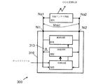
図1は、駆動回路110および共振アンテナ回路101を備える送信機デバイス100の高水準ブロック図を示す。
FIG. 1 shows a high level block diagram of a
共振アンテナ回路101は、励起された後に発振電圧Voscを提供する2つのノードNa1およびNa2を有する。共振アンテナ回路101は、好ましくは、並列に接続されたインダクタンスLおよびコンデンサCを備えるパッシブ回路である。そのような回路は、「並列LC」回路または「並列RLC」回路として当技術分野で知られている。
The
図1の駆動回路110は、アンテナ回路101のノードNa1およびNa2に接続された2つのインターフェースノードのNi1およびNi2を有する。駆動回路110は、共振アンテナ回路101によって提供される発振電圧信号Voscの特徴を測定するように、および該発振電圧信号Voscのタイミング情報および振幅情報を抽出するように適合される制御回路103を含む。タイミング情報および振幅情報は、同じく駆動回路110の一部である励起回路102に提供される。励起回路102は、該タイミング情報に基づいて、および該振幅情報に基づいて励起信号を発生させるように適合され、また、該励起信号をインターフェースノードNi1、Ni2に、したがって、共振アンテナ回路101に印加するように適合される。
The
送信機デバイス100の作動は、図2から理解することができ、該図は、発振電圧Vosc、および(駆動回路によって明示的に使用されるのではなく、例示の目的で示される)インダクタンスLとキャパシタンスCとの間でアンテナ回路の内部を流れる電流Ioscを含む、一組の例示的な波形を示す。本発明の実施形態において、制御回路103は、黒い点で示されるように、発振電圧信号Voscが極小に到達する瞬間を決定する。図2において、黒色の点は、点線Vminを介して例示の目的で相互接続される。これらの極小電圧の振幅を比較することによって、制御回路は、発振電圧の電圧スイングが増加または減少していることを検出することができ、また、それに応じて、例えば振幅を実質的に一定に保つために、励起回路を調整することができる。
The operation of the
駆動回路110はまた、黒色の正方形によって示されるように、極小の検出の代わりに、またはそれと組み合わせて、発振電圧信号Voscの極大を検出するように適合させることもできる。図2では、極大も同様に、例示の目的で、点線Vmaxを介して接続される。
The
図2から認識することができるように、極小のタイミングもしくは振幅、または極大のタイミングもしくは振幅のいずれか、またはその両方を使用して、発振電圧Voscの電圧スイングを決定することができる。共振回路を「開始」したときには(図11も参照されたい)、発振電圧Vosc振幅または電圧スイングを増加させるために、励起パルスが共振アンテナ回路101に提供される。本発明において、1つまたは複数の励起パルスは、極小または極大の近傍に位置付けられる時間ウインドウ中に提供され、ウインドウの位置は、発振電圧の発振毎に決定される(図10でさらに論じられる)。本発明の実施形態において、時間ウインドウが極大の近傍に位置する場合、それは、極大に隣接している極小の間に位置する。本発明の実施形態において、時間ウインドウが極大の近傍に位置する場合、それは、極大に隣接している極小の間に位置する。時間ウインドウは、例えば、これらの極大もしくは極小の直前に、またはその直後に、またはその周囲に位置付けることができる。時間ウインドウが極大または極小の直前に位置する場合、時間ウインドウの終わりと、極小または極大との間の時間は、例えば、発振期間Toscの30%未満、またはさらに20%未満、またはさらに10%未満、またはさらに5%未満であり得る。時間ウインドウが極大または極小の直後に位置する場合、極小または極大と、時間ウインドウの始まりとの間の時間は、例えば、発振期間Toscの30%未満、またはさらに20%未満、またはさらに10%未満、またはさらに5%未満であり得る。図10に示される実施例において、ウインドウは、時間ウインドウの発生直前に開始し、極小に到達した直後に停止するように選択されるが、他の解決策も使用することができ、例えば、時間ウインドウは、極小の位置で開始し、例えばローカルクロックによって決定される、所定の持続時間を有することができる。本発明の実施形態において、通電パルスは、好ましくは、時間ウインドウにだけ提供される。
As can be appreciated from FIG. 2, either the minimum timing or amplitude, or the maximum timing or amplitude, or both, can be used to determine the voltage swing of the oscillating voltage Vosc. When the resonance circuit is “started” (see also FIG. 11), an excitation pulse is provided to the
通電パルスが印加される時間ウインドウは、好ましくは、発振期間Toscの60%未満、またはさらに50%未満、またはさらに30%未満、またはさらに20%未満に選択される。 The time window during which the energization pulse is applied is preferably selected to be less than 60%, or even less than 50%, or even less than 30%, or even less than 20% of the oscillation period Tosc.
本発明の大きな利点は、いくつかの従来技術とは対照的に(連続伝送中に)発振が中断されないので、時間ウインドウの正確な開始および持続時間が電流印加に関して重要でないこと、および、アンテナ回路の共振周波数と同一である発振周波数に悪影響を及ぼさないことである。 The great advantage of the present invention is that the exact start and duration of the time window is not important with respect to current application since the oscillation is not interrupted (during continuous transmission) as opposed to some prior art, and the antenna circuit The oscillation frequency, which is the same as the resonance frequency, is not adversely affected.
発振電圧Voscの周波数は、駆動回路110の構成要素が共振回路のLとCとの間で直列に接続されないので、共振アンテナ回路101の構成要素L、Cによって、またごくわずかに駆動回路110の構成要素によって、一次的に、またはほぼ排他的に決定される。駆動回路110は、基本的に発振電圧Voscの振幅に、および間接的に共振システムを通って流れる電流にだけ影響を及ぼすが、発振期間Tosc、したがって、発振周波数Fosc=1/Toscに大きな影響を及ぼさないように設計される。さらに、駆動回路110は、共振回路101の損失に積極的に関与せず、それ故に、共振システムの全体的な線質係数または損失にいかなる悪影響も及ぼさない。
The frequency of the oscillating voltage Vosc is such that the components of the
本発明の根本原理によれば、励起パルス112の形状、および/またはサイズ、および/または数(それ故に、時間ウインドウ中に共振アンテナ回路の中へ注入されるパルスのエネルギー含量)は、発振電圧Voscの測定された振幅値に依存して、例えば極小の振幅または極大の振幅またはその両方の関数として選択される。 In accordance with the underlying principles of the present invention, the shape and / or size and / or number of excitation pulses 112 (and hence the energy content of the pulses injected into the resonant antenna circuit during the time window) is determined by the oscillation voltage. Depending on the measured amplitude value of Vosc, it is selected, for example, as a function of a minimum amplitude or a maximum amplitude or both.
駆動回路110は、基本的に以下の4つの動作モードを有する。
−オフ:アンテナ回路に通電パルスを提供しないモード
−開始:例えば電圧スイングが所定のレベルに到達するまで電圧スイングを増加させるように選択される、通電パルスを提供するモード
−オン:発振電圧振幅を可能な限り一定に保つように通電パルスを提供するモード
−停止:例えばいかなるパルスも送信しないことによって(パッシブ)、または「停止パルス」を送信することによって(アクティブ)、発振電圧振幅をアクティブまたはパッシブに減少させるモードそのようなパルスの停止は、上で論じた時間ウインドウの外側で送信することができる。
The
-Off: Mode that does not provide energization pulses to the antenna circuit-Start: Mode that provides energization pulses, for example, selected to increase the voltage swing until the voltage swing reaches a predetermined level-On: Oscillation voltage amplitude Mode that provides energized pulses to keep them as constant as possible-Stop: Active or passive oscillation voltage amplitude, eg by not sending any pulse (passive) or by sending a "stop pulse" (active) Such a pulse stop can be transmitted outside the time window discussed above.
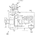
図3は、本発明の第2の実施形態による、送信機デバイス300および駆動回路310の高水準ブロック図を示し、該図は、図1の送信機デバイス100および駆動回路110の変形として認識することができる。
FIG. 3 shows a high level block diagram of a
図1の実施形態では、開始および停止に必要とされる時間がその用途(搬送波形を送信すること)には重要でなかったが、図3の装置および回路に関しては、高速開始および高速停止が重要である。上で説明したブロックおよび機能性に加えて、駆動回路310は、ダンパー回路304をさらに備え、該ダンパー回路は、例えば、インターフェーシングノードNi1とNi2との間でエネルギーを消散させるための1つ以上の抵抗器をスイッチによってアンテナに並列に加えることによって、またはキャパシタをアンテナに並列に加えることによって、または逆位相電流パルスをアンテナ回路に注入することによって実現することができる。いくつかの従来技術の解決策とは対照的に、そのようなスイッチは、通常動作中に共振回路のLとCとの間で直列に接続されるのではなく、発振を停止させる必要があるときにだけ接続されることに留意されたい。
In the embodiment of FIG. 1, the time required to start and stop was not important for the application (transmitting the carrier waveform), but for the apparatus and circuit of FIG. is important. In addition to the blocks and functionality described above, the
図3のデバイスおよび回路と、図1のデバイスおよび回路との別の違いは、駆動回路310が、(例えば、外部プロセッサのUARTから)バイナリビットストリームを受信するための入力ポートを有することである。
Another difference between the device and circuit of FIG. 3 and the device and circuit of FIG. 1 is that the
制御回路303は、伝送されるビットストリームの値に応じて、開始〜オンを介したモードオフからの高速な変化に、および停止〜オフを介したモードオンからの高速な変化にさらに適合される。好ましくは、開始および停止の持続時間は、できる限り短い。
The
より具体的には、本発明の実施形態において、「開始」は、5.0未満のTosc期間、例えば4.0未満のTosc期間、例えば3.0未満のTosc期間、例えば2.0未満のTosc期間、例えば約0.5〜約1.5未満のTosc期間をとり、これは、この時間の後に、発振電圧Voscの振幅が、約0からその公称値の95%を超えるまで増加することを意味する。 More specifically, in embodiments of the present invention, “start” refers to a Tosc period of less than 5.0, such as a Tosc period of less than 4.0, such as a Tosc period of less than 3.0, such as less than 2.0. Take a Tosc period, for example, a Tosc period of about 0.5 to less than about 1.5, after which time the amplitude of the oscillating voltage Vosc increases from about 0 to over 95% of its nominal value. Means.
同様に、本発明の実施形態において、「停止」は、5.0未満のTosc期間、例えば4.0未満のTosc期間、例えば3.0未満のTosc期間、例えば2.0未満のTosc期間、例えば約0.5〜約1.5未満のTosc期間をとり、これは、この時間の後に、発振電圧Voscの振幅が、その公称値からその公称値の5%未満まで減少することを意味する。 Similarly, in an embodiment of the present invention, “stop” refers to a Tosc period of less than 5.0, such as a Tosc period of less than 4.0, such as a Tosc period of less than 3.0, such as a Tosc period of less than 2.0, For example, taking a Tosc period of about 0.5 to less than about 1.5, this means that after this time the amplitude of the oscillating voltage Vosc decreases from its nominal value to less than 5% of its nominal value. .
図2に関して論じられる原理と同じ原理を使用することで、すなわち、発振電圧Voscを監視することによって、および発振電圧が極小または極大または両方に到達した時間を検出することによって、およびこれらの極大または極小の振幅を測定することによって、およびこれらの局所的極度の周囲に、または直前に、または直後に、または別様には近傍に位置付けられる時間ウインドウの中に適切なサイズおよび/または形状および/または数を有する1つ以上の励起パルスを印加することによって、共振アンテナ回路の損失にもかかわらず、発振電圧Voscの振幅を実質的に一定に保つことが可能である。 By using the same principle as discussed with respect to FIG. 2, ie by monitoring the oscillating voltage Vosc and detecting the time when the oscillating voltage has reached a minimum or maximum or both, and these maximum or Appropriate size and / or shape and / or by measuring the minimum amplitude and within a time window located around, just before, immediately after, or otherwise in the vicinity of these local extremes Alternatively, by applying one or more excitation pulses having a number, it is possible to keep the amplitude of the oscillation voltage Vosc substantially constant despite the loss of the resonant antenna circuit.
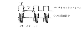
図4は、一実施例として(しかし、示される発振の数は、実際に使用される数よりもはるかに少ない)、どのように図4の駆動回路310を、例えばPEPSまたはPKEなどの「パッシブエントリ用途」で使用することができる、OOK変調信号(オン−オフキーイング)を伝送するために使用することができるのかを例示する。バイナリビットストリームは、典型的には、「UART」を有するマイクロコントローラによって提供されるが、本発明は、これに限定されず、ビットストリームはまた、例えばタイマー割り込みを使用するマイクロコントローラによる、または所定のクロックで動いているプログラム可能なハードウェアもしくは状態機械によるなどの、他の方法でも提供することができるが、本発明の主眼ではない。
FIG. 4 shows, as an example (however, the number of oscillations shown is much less than the number actually used) how to make the
図4の実施例において、バイナリビットストリームの値が「1」である間、駆動回路は、共振アンテナ回路の発振を維持するためのオンモードである。バイナリビットストリームの立ち下がりエッジで、駆動回路は、停止モードから進むことによって、素早く共振アンテナ回路の発振を停止し、次いで、オフモードへ進む。バイナリビットストリームの値が「0」である間、駆動回路は、オフモードであり、共振アンテナ回路の振動を随意に抑制することができる。バイナリビットストリームの立ち上がりエッジで、駆動回路は、素早く共振アンテナ回路の発振を開始し、次いで、オンモードへ進む。 In the embodiment of FIG. 4, while the value of the binary bit stream is “1”, the driving circuit is in an on mode for maintaining oscillation of the resonant antenna circuit. At the falling edge of the binary bit stream, the drive circuit quickly stops oscillation of the resonant antenna circuit by proceeding from the stop mode and then proceeds to the off mode. While the value of the binary bit stream is “0”, the drive circuit is in the off mode, and the vibration of the resonant antenna circuit can be suppressed arbitrarily. At the rising edge of the binary bitstream, the driver circuit quickly starts oscillating the resonant antenna circuit and then proceeds to the on mode.
図5は、本発明の第3の実施形態による、送信機デバイス500および駆動回路510のより詳細なブロック図を示す。この駆動回路は、図3の駆動回路310と同じ機能性を有するが、それに加えて、1つ以上の所定のDC電圧、例えば比較的大きい正電圧Vp(例えば、最高で約+100V)および/または比較的大きい負電圧Vn(例えば、最高で約−100V)を提供するための、1つ以上の電圧発生器回路を備える。特定の実施形態では、正のDC電圧Vpおよび負のDC電圧Vnを同時に発生させるための2つの電圧発生器が存在する。代替の実施形態において、これらの電圧源または電圧発生器はまた、駆動回路自体の外側に位置付けることもできる。
FIG. 5 shows a more detailed block diagram of a
図5の実施形態において、通電パルスは、所与の時間ウインドウ中に1つ以上の電流パルスを発生させるように適合される、電流源「I_パルス」によって発生される電流パルスである。上で説明したように、1つ以上の電流パルスのエネルギー含量、例えば電流パルスの形状、および/またはサイズ、および/または数は、測定された発振電圧Voscの振幅に依存する。 In the embodiment of FIG. 5, the energization pulse is a current pulse generated by a current source “I_pulse” that is adapted to generate one or more current pulses during a given time window. As explained above, the energy content of one or more current pulses, for example the shape and / or size and / or number of current pulses, depends on the amplitude of the measured oscillating voltage Vosc.
いくつかの随意選択が可能であり、そのいくつかを以下に列記する。
a)時間ウインドウあたり単一のパルスだけが送信され、該パルスは、所定の持続時間を有するが、測定されたVoscの振幅に応じて、調整可能な振幅を有する。
b)時間ウインドウあたり単一のパルスだけが送信され、該パルスは、所定の振幅を有するが、測定されたVoscの振幅に応じて、調整可能な持続時間を有する。
c)時間ウインドウあたり単一のパルスだけが送信され、該パルスは、測定されたVoscの振幅に応じて、調整可能な振幅および調整可能な持続時間を有する。
d)時間ウインドウあたり固定の所定数のパルス、例えば約8または約16または約24のパルスが送信される。これらのパルスの各々は、測定されたVoscの振幅に応じて、固定の持続時間および調整可能な振幅、または固定の振幅および調整可能な持続時間、または調整可能な持続時間および調整可能な振幅、調整された時間および/または振幅を有することができる。
e)時間ウインドウあたり調整可能な数のパルスが送信され、該パルス数は、測定された発振電圧Voscの振幅に依存する。パルスは、測定されたVoscの振幅に応じて、固定の持続時間および固定の振幅、または固定の振幅および調整可能な持続時間、または固定の持続時間および調整可能な振幅、または調整可能な持続時間および調整可能な振幅、調整された時間および/または振幅を有することができる。
Several options are possible, some of which are listed below.
a) Only a single pulse is transmitted per time window, which has a predetermined duration but an adjustable amplitude depending on the measured amplitude of Vosc.
b) Only a single pulse is transmitted per time window, which pulse has a predetermined amplitude, but has an adjustable duration depending on the measured Vosc amplitude.
c) Only a single pulse is transmitted per time window, which has an adjustable amplitude and an adjustable duration, depending on the measured amplitude of Vosc.
d) A fixed predetermined number of pulses per time window, eg about 8 or about 16 or about 24 pulses are transmitted. Each of these pulses has a fixed duration and an adjustable amplitude, or a fixed amplitude and an adjustable duration, or an adjustable duration and an adjustable amplitude, depending on the measured Vosc amplitude, It can have an adjusted time and / or amplitude.
e) An adjustable number of pulses are transmitted per time window, the number of pulses depending on the amplitude of the measured oscillation voltage Vosc. The pulse may have a fixed duration and fixed amplitude, or a fixed amplitude and adjustable duration, or a fixed duration and adjustable amplitude, or an adjustable duration, depending on the measured Vosc amplitude. And adjustable amplitude, adjusted time and / or amplitude.
正の通電電圧Vpおよび負の通電電圧Vnがどちらも利用可能である特定の実施形態では、正電流パルスおよび/または負電流パルスのどちらも提供することができる。これは、さらに高速な開始および/または停止を可能にすることができる。 In certain embodiments where both positive energization voltage Vp and negative energization voltage Vn are available, both positive and / or negative current pulses can be provided. This can allow for faster start and / or stop.
図5に示される具体的な実施例において、制御ブロック503は、以下のサブブロックのうちの1つ以上および好ましくはすべてを含むことができる。
−発振電圧Voscの極小の発生を検出するための最小電圧検出器(MVD)
−Voscの極小電圧に到達した時間を決定するための最小交差検出器(MCD)
−測定された電圧振幅または電圧スイングと意図する電圧、例えば基準電圧または公称電圧との差を決定するための誤り発生器
−変調器、具体的にはOOK変調器
In the specific example shown in FIG. 5, the
A minimum voltage detector (MVD) for detecting the minimal occurrence of the oscillation voltage Vosc
A minimum cross detector (MCD) to determine the time to reach the minimum voltage of Vosc
An error generator for determining the difference between the measured voltage amplitude or voltage swing and the intended voltage, for example a reference voltage or a nominal voltage; a modulator, in particular an OOK modulator
測定された発振電圧Voscの振幅に応じて、単一の電流パルスの振幅を、例えば32の所定の振幅値のうちの1つとして選択することができる。特定のウインドウ中に送信された電流パルスは、すべてが同じサイズおよび振幅を有することができるが、そうである必要はなく、該電流パルスはまた、異なる振幅、および/またはサイズ、および/または持続時間、および/または形状(例えば、矩形、台形、三角形、ガウシアン、またはこれらの組み合わせ)も有することができる。パルス持続時間、および/またはパルスの立ち上がりエッジの傾斜、および/または立ち下がりエッジの傾斜のうちの1つ以上などの、パルスの特徴は、測定された発振電圧Voscの振幅の関数として、動的に適合させることができる。 Depending on the measured amplitude of the oscillating voltage Vosc, the amplitude of a single current pulse can be selected as one of 32 predetermined amplitude values, for example. Current pulses transmitted during a particular window can all have the same size and amplitude, but this need not be the case, and the current pulses can also be of different amplitude and / or size and / or duration. It can also have time and / or shape (eg, rectangular, trapezoidal, triangular, Gaussian, or combinations thereof). The characteristics of the pulse, such as one or more of the pulse duration and / or the slope of the rising edge of the pulse and / or the slope of the falling edge, can be expressed as a function of the amplitude of the measured oscillating voltage Vosc. Can be adapted.
電流パルスは、PLL(フェーズロックループ)を使用して、発振電圧Voscに同期させたローカルクロック信号から導出することができる。この手法の利点は、ローカな水晶発振器を回避すること(コストの低減および/またはピン数の低減)ができることである。 The current pulse can be derived from a local clock signal synchronized to the oscillating voltage Vosc using a PLL (phase locked loop). The advantage of this approach is that a local crystal oscillator can be avoided (reduced cost and / or reduced pin count).
別の実施形態において、電流パルスは、例えばローカル水晶またはローカル水晶モジュールによって発生させることができる、発振電圧Voscとは非同期である別個のクロック信号から導出することができる。示される実施例では、32MHzの外部水晶が使用されるが、本発明は、それに制限されるものではなく、また、別の周波数の水晶または水晶モジュールも使用することができる。電流パルスが送信されるタイミングを発生させるために、非同期クロックを使用することの利点は、電流パルスが発振信号Voscと(マイクロレベルで)同期しておらず、あまり鋭くないパルスを作り出すことができ、したがって、EMCにより良いものになり得る。想定される用途の場合、発振電圧foscの周波数は、典型的には、およそ10kHz〜250kHzであり、水晶の周波数は、典型的には、およそ10MHz〜50MHzであり、それ故に、ローカルクロック周波数と発振アンテナ周波数との比率は、典型的には、40〜5000の範囲、例えば、100〜1000の範囲の値である。 In another embodiment, the current pulse can be derived from a separate clock signal that is asynchronous with the oscillating voltage Vosc, which can be generated, for example, by a local crystal or a local crystal module. In the embodiment shown, a 32 MHz external crystal is used, but the invention is not so limited, and other frequency crystals or crystal modules can also be used. The advantage of using an asynchronous clock to generate the timing at which the current pulse is transmitted is that the current pulse is not synchronized (at the micro level) with the oscillating signal Vosc and can produce pulses that are not very sharp. Therefore, it can be better for EMC. For the envisaged applications, the frequency of the oscillating voltage fosc is typically about 10 kHz to 250 kHz, and the frequency of the crystal is typically about 10 MHz to 50 MHz, hence the local clock frequency and The ratio with the oscillation antenna frequency is typically a value in the range of 40 to 5000, for example, in the range of 100 to 1000.
駆動回路510は、随意に、スペクトラム拡散技術を使用して、電流パルスによって発生される高調波のピーク高さをさらに低減させるための更なる回路を備えることができる。これを達成するための1つの方法は、すべてが同じ「オン時間」を有しないパルスのバーストを使用することである(図7は、オン時間が何を意味するのかを示す)。例えば、中央整列PWM信号のデューティサイクルを修正することによって、または例えば左整列と、中央整列と、右整列との間で、単一の時間ウインドウの内側で、または異なる時間ウインドウの間でPWM信号の整列を変化させることによって、オン時間を変動させることで、スペクトラムのピーク高さをさらに低減させることができる。
The
本発明による駆動回路の具体的な利点は、該駆動回路が、例えば6つの共振回路を駆動する必要がある共振アンテナ回路501あたり(図5に1つだけ示される)、2つのパッドまたはピンだけしか必要としないことである。実際に、各共振アンテナ回路のピンの1つが第1のインターフェースピンNi1に接続されている場合は、6つの共振アンテナ回路を駆動するために、6つの追加のインターフェースピンNi2だけしか必要とされない。集積チップのピン数は、そのようなチップのコストにおける重要な要素であるので、これらの実施形態はどちらも、従来技術に勝る重要な利点であると考えられる。当然、6つという数字は一例に過ぎず、本発明は、その数に制限されない。 A particular advantage of the drive circuit according to the invention is that it only needs two pads or pins per resonant antenna circuit 501 (only one is shown in FIG. 5), for example, where the drive circuit needs to drive six resonant circuits. It is only necessary. In fact, if one of the pins of each resonant antenna circuit is connected to the first interface pin Ni1, only six additional interface pins Ni2 are required to drive the six resonant antenna circuits. Both of these embodiments are considered significant advantages over the prior art because the number of pins of an integrated chip is an important factor in the cost of such a chip. Of course, the number of 6 is only an example, and the present invention is not limited to that number.
特に興味深い実施形態において、電圧源または電圧発生器回路は、負の駆動電圧Vnを提供し、駆動回路510は、標準的な同軸ケーブルによって1つ以上の共振アンテナ回路501に接続され、接地電位がシールド電圧として使用され、同軸ケーブルの中央には高電圧駆動信号が印加される。これは、エンドユーザの良好な保護を可能にする。
In a particularly interesting embodiment, the voltage source or voltage generator circuit provides a negative drive voltage Vn, and the
図6は、図5のブロック図の原理のいくつかを説明する、例示的な一組の波形を示す。具体的には、駆動回路510に供給することができる、または駆動回路510の1つ以上の電圧発生器回路によって発生させることができる、正電圧Vpおよび負電圧Vnを示す。
FIG. 6 shows an exemplary set of waveforms that illustrate some of the principles of the block diagram of FIG. Specifically, a positive voltage Vp and a negative voltage Vn that can be supplied to the
上で説明したように、オンモード中に、パルス112は、典型的には、発振電圧Voscの振幅が実質的に一定の状態を維持するように選択される。図6に示される実施例において、単一のパルス112だけが各時間ウインドウに提供される。時間ウインドウ自体は示されていないが、発振電圧Voscが極小に到達する時間とほぼ同じ時間に位置付けられる。電流パルスが印加される正確な瞬間は、本発明に関しては重要でない。
As explained above, during the on mode, the
誤り信号ERRも示されているが、これは、この実施例において、Voscの実際の振幅とVoscの所望の振幅との差として定義される。上で説明したように、この誤り信号ERRを使用して、発振電圧Voscの振幅を増加させるために、電流パルスのサイズ、および/または形状、および/または数を調整することができる。 An error signal ERR is also shown, which in this example is defined as the difference between the actual amplitude of Vosc and the desired amplitude of Vosc. As explained above, this error signal ERR can be used to adjust the size and / or shape and / or number of current pulses in order to increase the amplitude of the oscillating voltage Vosc.
図7は、本発明の実施形態において使用することができる、例示的なパルス形状を示す。電流パルスは、示されるように、台形形状を有することができ、所定の持続時間を有する立ち上がりエッジ「Trize」と、所定の持続時間を有する一定の部分「オン時間」と、所定の持続時間を有する立ち下がりエッジ「Tdown」とを備える。 FIG. 7 illustrates an exemplary pulse shape that can be used in embodiments of the present invention. The current pulse can have a trapezoidal shape, as shown, with a rising edge “Trize” having a predetermined duration, a constant portion “on time” having a predetermined duration, and a predetermined duration. And a falling edge “Tdown”.
Trise、Tdown、およびTonの値は、設計した時間での、さらにはデバイスの実際の使用中に動的に、高調波(EMC)の発生を低減させる、例えば最小にするように選択することができる。示される実施例では、パルス持続時間(オン時間)が固定されているが、振幅は、誤り信号ERRの関数として調整される。誤り信号が大きくなるほど、すなわち想定される振幅からのずれが大きくなるほど、パルスの振幅が大きくなる。任意の適切な関数、例えば比例関数、一次関数(=比例+オフセット)、二次機能、階段関数、区分線形関数(例えば、ルックアップテーブルに基づく)、または任意の他の適切な関数を使用することができる。図6に示される実施例において、電流パルスは、MCDの立ち上がりエッジ(極小が検出された場所)毎に注入される。 The values of Trise, Tdown, and Ton may be selected to reduce, eg minimize, the generation of harmonics (EMC) at the designed time and even dynamically during actual use of the device. it can. In the example shown, the pulse duration (on time) is fixed, but the amplitude is adjusted as a function of the error signal ERR. The larger the error signal, that is, the greater the deviation from the assumed amplitude, the greater the amplitude of the pulse. Use any suitable function, eg proportional function, linear function (= proportional + offset), quadratic function, step function, piecewise linear function (eg based on lookup table), or any other suitable function be able to. In the embodiment shown in FIG. 6, a current pulse is injected at every rising edge of the MCD (where a local minimum is detected).
台形形状を有するパルスは、周波数スペクトルにおけるスプリアス信号の発生が少ないので、該パルスを有することが利点であり、これは、EMCの理由から有利である。しかし、本発明は、このパルス形状だけに限定されるものではなく、他のパルス形状、例えば、ドーム形状、または正弦波形状、三角形パルスもしくはガウシアン形状、または任意の他の適切な形状も使用することができ、または一部のパルスが第1の形状(例えば、台形)を有することができ、他のパルスが第1の形状と異なる第2の形状(例えば、三角形)を有することができる。 A pulse with a trapezoidal shape has the advantage of having a pulse because it produces less spurious signals in the frequency spectrum, which is advantageous for EMC reasons. However, the present invention is not limited to this pulse shape, but also uses other pulse shapes such as a dome shape, or a sinusoidal shape, a triangular pulse or a Gaussian shape, or any other suitable shape. Or some pulses can have a first shape (eg, trapezoid) and other pulses can have a second shape (eg, a triangle) different from the first shape.
図8は、各時間ウインドウにおいて単一のパルスだけが使用されるのではなく、各時間ウインドウにおいて複数のパルスが使用される、別の実施形態を示す。 FIG. 8 shows another embodiment where multiple pulses are used in each time window rather than only a single pulse in each time window.
これらのパルスの各々の持続時間、およびサイズ、および形状は、予め定義し、固定することができるが、各時間ウインドウにおいて印加されるパルスの数は、誤り信号ERRの関数として決定される。誤り信号が(絶対値で)大きくなるほど、注入されるパルス数が多くなる。パルスは、好ましくは、時間ウインドウの内側で、小さいバーストにおいて印加される。 The duration, size, and shape of each of these pulses can be predefined and fixed, but the number of pulses applied in each time window is determined as a function of the error signal ERR. The larger the error signal (in absolute value), the more pulses are injected. The pulses are preferably applied in small bursts inside the time window.
図8に示されるパルスの形状は、矩形であるが、他のパルス形状、例えば台形、三角形、正弦波状、または任意の他の適切な形状も使用することができる。図8に示されるパルスは、すべて同じ形状およびサイズを有するが、同じく、そうである必要はなく、パルスは、異なる振幅およびサイズを有することができる。 The pulse shape shown in FIG. 8 is rectangular, but other pulse shapes such as trapezoidal, triangular, sinusoidal, or any other suitable shape may be used. The pulses shown in FIG. 8 all have the same shape and size, but need not be as well, and the pulses can have different amplitudes and sizes.
図8の特定の変形(図示せず)では、最高で例えば8つのパルスが各時間ウインドウにおいて送信され、該パルスは、2の累乗の予め定義された相対振幅を有する。したがって、(送信される、またはされない)第1のパルスは、128ユニットの振幅を有し、(送信される、またはされない)第2のパルスは、64ユニットの振幅を有する、などである。これらの所定のパルスの各々は、実際に送信されたかどうかにかかわらず、測定された発振電圧Voscの振幅の値に依存する。 In the particular variant of FIG. 8 (not shown), at most, for example, 8 pulses are transmitted in each time window, which pulses have a predefined relative amplitude of powers of 2. Thus, the first pulse (transmitted or not) has an amplitude of 128 units, the second pulse (transmitted or not) has an amplitude of 64 units, and so on. Each of these predetermined pulses depends on the value of the amplitude of the measured oscillating voltage Vosc, whether or not it is actually transmitted.
図9は、オンモードでの通常動作中に、図5の回路において使用/取得することができる、例示的な一組の波形を示す図である。いくつかの信号が示されている(図の上部の見出しを参照されたい)。 FIG. 9 is a diagram illustrating an exemplary set of waveforms that can be used / acquired in the circuit of FIG. 5 during normal operation in the on mode. Several signals are shown (see heading at the top of the figure).
第1の信号は、「Vmin」と呼ばれ、この信号は、特定の実現形態のため、この実施例において、鋸歯状波形に類似している。この概念は、Vminが、Voscの最小値を追跡または「追従」し、Voscが急に増加したときに、Vminは、時間とともに(典型的には、RC定数によって)緩やかに減衰する。(詳細は、図11を参照されたい)。このような信号を作製するための回路は、当技術分野で知られており、また、例えば、ダイオードと、抵抗器Rと、キャパシタCと、比較器とを備えることができるが、他の回路も使用することができる。 The first signal is referred to as “Vmin”, and this signal is similar to the sawtooth waveform in this example for the particular implementation. This concept follows that Vmin tracks or “follows” the minimum value of Vosc, and when Vosc suddenly increases, Vmin decays slowly over time (typically by the RC constant). (See Figure 11 for details). Circuits for producing such signals are known in the art and can include, for example, diodes, resistors R, capacitors C, and comparators, but other circuits. Can also be used.
示される実施例において、各極小毎の時間ウインドウは、信号「Vmin」が信号「Vosc」と交差するときに開始するが(詳細は、図10を参照されたい)、本発明は、この実現形態に限定されるものではなく、他の時間ウインドウも使用することができる。 In the example shown, the time window for each minimum starts when the signal “Vmin” crosses the signal “Vosc” (see FIG. 10 for details), but the present invention implements this implementation. However, other time windows can be used.
もう1つの信号は「Vpulse」であり、図9において黒色の太線セグメントとして表されているが、実際には、図10においてさらに詳細に論じられるように、パルス信号のバーストである。 Another signal is “Vpulse”, which is represented as a thick black line segment in FIG. 9, but is actually a burst of pulse signals, as discussed in more detail in FIG.
もう1つの信号は「Vosc」であり、これは、共振アンテナ回路501によって提供される電圧信号である。
Another signal is “Vosc”, which is a voltage signal provided by the
図9から認識することができるように、発振は、極めて安定した周波数を有する正弦波状信号である。振幅は変動し得るが、駆動回路によって、アンテナ回路における放射エネルギーおよび損失を補償するための必要なエネルギーを提供する励起パルスのおかげで、実質的に一定に保たれる。 As can be appreciated from FIG. 9, the oscillation is a sinusoidal signal having a very stable frequency. The amplitude can vary, but is kept substantially constant by the drive circuit, thanks to an excitation pulse that provides the necessary energy to compensate for radiant energy and losses in the antenna circuit.
図10は、図9に示される波形のいくつかを拡大図で示す。この実施例において、時間ウインドウは、「Vosc」が「Vmin」をよりも大きくなったときに、したがって、「Vmin」信号が「Vosc」曲線にもはや追従しないが、減衰する場合に停止する。 FIG. 10 shows in enlargement some of the waveforms shown in FIG. In this example, the time window stops when “Vosc” becomes greater than “Vmin”, and therefore when the “Vmin” signal no longer follows the “Vosc” curve but decays.
図10の底部には、一連の制御パルスが示され、これらは、その後に、実際の電流パルス信号を発生させるために使用される。このような制御パルスは、デジタル回路によって発生させることができる。 At the bottom of FIG. 10, a series of control pulses are shown, which are then used to generate the actual current pulse signal. Such a control pulse can be generated by a digital circuit.
既に述べたように、本発明はこの特定の実現形態に限定されるものではなく、他の時間ウインドウも使用することもできる。 As already mentioned, the present invention is not limited to this particular implementation, and other time windows can be used.
図11は、開始モード中に、図5の回路において使用/取得することができる、例示的な一組の波形を示す。初期パルスまたはパルスのバースト(図示せず)の後に、アンテナ回路は、比較的小さい値の発振電圧信号Voscを発生させ始めるが、その瞬間から、駆動回路510は、開始モード中に説明した機構と同じ機構を使用し、すなわち、発振電圧信号を監視することによって、極小および/または極大を見出し、適切な時間ウインドウを見出し、または選択し、そして、該時間ウインドウにおいて1つ以上の電流パルスを提供する。しかしながら、開始中に、電流パルスのエネルギーは、より高速の開始を得るために、オンモード中に必要とされるエネルギーよりも大きく、例えばできる限り大きく選択することができる。
FIG. 11 illustrates an exemplary set of waveforms that can be used / acquired in the circuit of FIG. 5 during start mode. After an initial pulse or burst of pulses (not shown), the antenna circuit begins to generate a relatively small value of the oscillating voltage signal Vosc, but from that moment on, the
図12は、本発明の一実施形態による、送信機デバイス1200および駆動回路1210の別のブロック図を示す。この装置1200および回路1210の機能性は、図3および図5に示される機能性に類似するか、または同一であるが、電圧源VpおよびVnが明示的に示される。これらの電圧は、(示されるように)外部回路によって提供することができ、または駆動回路1210の一部とすることができる、1つ以上の電圧発生器によって提供することができる。
FIG. 12 shows another block diagram of a
2つの独立した比較的高い電圧の発生器を使用することによって、例えば接地の代わりに負電圧を使用し、正電圧の代わりに接地を使用して、駆動信号を反転させることが可能であることが想定される。これは、2つの高い電圧(例えば、比較的長い、例えば1mよりも長いケーブルを通じて、およそ+100Vおよび−100V)を提供することに勝る利点を有し得る。 By using two independent relatively high voltage generators, it is possible to invert the drive signal, for example using a negative voltage instead of ground and using ground instead of positive voltage Is assumed. This may have advantages over providing two high voltages (eg, approximately + 100V and −100V through a relatively long cable, eg, longer than 1 m).
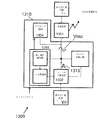
図13は、本発明の一実施形態による、送信機デバイス1300および駆動回路1310の別のブロック図を示す。これは、図12に示されるブロック図の変形とみなすことができるが、シグマ−デルタ変調器およびバースト長デターミネータという2つの主な違いがあり、(別個のブロックとして示されているが)どちらも制御回路1310の一部である。シグマ−デルタ変調器の目的は、予め定義されたパルス間の時間間隔を伴う所定の「オン時間」(図7を参照されたい)を有する、パルスのバーストを発生させることである。パルス間の時間は、固定した所定の値とすることができ、または変数として、「誤り発生器」によって提供される(例えば、図6の誤り信号ERRから導出することができる)測定された発振電圧Voscの振幅に依存することができる。「バースト長デターミネータ」は、パルスがシグマ−デルタ変調器によって送信されている間の時間を、図8に関して説明したように、測定された振幅Voscの関数として決定する。
FIG. 13 shows another block diagram of a
図14は、本発明の一実施形態による、共振アンテナ回路を駆動する方法を示す図である。本方法は、a)共振アンテナ回路によって提供される発振電圧信号Voscを監視するステップ1401と、b)該発振電圧信号Voscのタイミング情報および振幅情報を抽出するステップ1402と、c)測定されたタイミング情報に基づいて、および測定された振幅情報に基づいて、励起信号を発生させ、該励起信号を共振アンテナ回路に印加するステップ1403と、を含む。
FIG. 14 is a diagram illustrating a method of driving a resonant antenna circuit according to an embodiment of the present invention. The method includes: a) a
タイミング情報を抽出することは、該発振電圧信号Voscの極小および/または極大を検出することを含むことができ、また、これらの極小または極大または両方の近傍に位置付けられる時間ウインドウを決定することを含むことができる。 Extracting the timing information can include detecting a minimum and / or maximum of the oscillating voltage signal Vosc, and determining a time window located in the vicinity of these minimum or maximum or both. Can be included.
本方法は、該発振電圧信号Voscの振幅を測定し、該振幅から、発振を維持するために共振アンテナ回路において注入する必要があるエネルギー量を示す、誤り信号を導出することをさらに含むことができる。 The method further includes measuring the amplitude of the oscillating voltage signal Vosc and deriving an error signal from the amplitude that indicates the amount of energy that needs to be injected in the resonant antenna circuit to maintain oscillation. it can.
ステップc)は、時間ウインドウ毎に単一の電流パルスまたは一連の電流パルスの形態で励起信号を発生させ、提供することを含むことができる。電流パルスは、正符号または負符号を有することができることに留意されたい。 Step c) can include generating and providing an excitation signal in the form of a single current pulse or a series of current pulses per time window. Note that the current pulse can have a positive or negative sign.
図15は、共振アンテナ回路の発振電圧Voscと、発振電圧が極小に到達した瞬間に単一の(比較的大きい)電流パルスが注入される時間との関係の例示的なシミュレーション波形を示す。 FIG. 15 shows an exemplary simulation waveform of the relationship between the oscillation voltage Vosc of the resonant antenna circuit and the time when a single (relatively large) current pulse is injected at the moment when the oscillation voltage reaches a minimum.
この実施例の背景にある概念は、以下の通りであり、共振回路の振幅を実質的に一定に保つために、(例えば、ダイオードと、RCと、比較器とを備える上述した回路を使用することによって)発振電圧を「監視する」こと、および発振電圧が極小に到達した瞬間に、単一の比較的小さい電流パルスを注入することを想定した。しかしながら、このような単一の比較的大きい電流パルスは、EMCに対して悪影響を有する、発振電圧信号の急な電圧の変化(すなわち、振幅歪み)を引き起こすことを見出した。この点において、スイッチを閉じることによってキャパシタが(急に)所定の電圧だけ再充電されるいくつかの従来技術の実施形態では、単一の大きい電流パルスも提供されることに留意されたい。 The concept behind this embodiment is as follows, in order to keep the amplitude of the resonant circuit substantially constant (for example, using the circuit described above comprising a diode, RC, and comparator): It was assumed that the oscillation voltage was "monitored" and that a single relatively small current pulse was injected at the moment when the oscillation voltage reached a minimum. However, it has been found that such a single relatively large current pulse causes an abrupt voltage change (ie, amplitude distortion) of the oscillating voltage signal, which has an adverse effect on the EMC. In this regard, it should be noted that in some prior art embodiments where closing the switch causes the capacitor to be recharged (abruptly) by a predetermined voltage, a single large current pulse is also provided.
EMCに対する電流パルスの影響を低減させる方法を模索することで、発明者らは、単一の比較的大きい電流パルスを使用するのではなく、同じ総エネルギー含量を有する複数の比較的小さい電流パルスを使用する、という概念に至った。しかし、おそらくは、さらに重要なことに、発明者らは、極小電圧に到達する前に既に、したがって、発振電圧波形の傾斜がまだゼロになっていない瞬間に、一連の電流パルスの注入を開始する、という概念に至った。 By seeking ways to reduce the effect of current pulses on EMC, we have used multiple relatively small current pulses with the same total energy content, rather than using a single relatively large current pulse. It came to the concept of using. But perhaps more importantly, the inventors start injecting a series of current pulses already before the minimum voltage is reached, and thus at the moment when the slope of the oscillating voltage waveform is not yet zero. I came up with the concept.
これは、注入されるエネルギーの量が、振幅の減少に依存し、最小に実際に到達するまで分からないので、些細な選択ということではない。さらに、「予測回路」を必要とするので、実現するのは些細なことでない。 This is not a trivial choice because the amount of energy injected depends on the decrease in amplitude and is not known until the minimum is actually reached. Furthermore, since a “prediction circuit” is required, it is not trivial to implement.
しかしながら、発振電圧Voscの「極小」を見出すために以前に使用されていた「最小検出回路」(上では「電圧監視回路」とも呼ばれる)を、細かな修正の後に、「予測手段」として、すなわち、「最小検出回路」の減衰信号「Vmin」が発振電圧Voscと交差する瞬間を検出するための回路を加えることによって、使用できることも見出した。同じ「最小検出回路」を、発振電圧Voscが最小検出回路の信号「Vmin」よりも速く上昇する時間として時間ウインドウの終了を定義したときに、時間ウインドウの終了を決定するためにも好都合に使用することができることをさらに見出した。とりわけ、(図16から認識することができるように)この時間ウインドウ中に注入される一連の電流パルスの引き起こす発振電圧信号の歪みがはるかに小さく、また、EMCの挙動に対する悪影響がはるかに低いことが分かった。 However, the “minimum detection circuit” (also referred to above as “voltage monitoring circuit”) that was previously used to find the “minimum” of the oscillating voltage Vosc is used as a “prediction means” after fine correction, that is, It has also been found that it can be used by adding a circuit for detecting the moment when the attenuation signal “Vmin” of the “minimum detection circuit” crosses the oscillation voltage Vosc. The same “minimum detection circuit” is also advantageously used to determine the end of the time window when the end of the time window is defined as the time when the oscillation voltage Vosc rises faster than the signal “Vmin” of the minimum detection circuit I have found that I can do more. In particular, the distortion of the oscillating voltage signal caused by the series of current pulses injected during this time window (as can be appreciated from FIG. 16) is much less and has a much lower adverse effect on the behavior of the EMC. I understood.
図16は、時間ウインドウの開始を予測するために使用される例示的なシミュレーション波形Voscおよび信号「Vmin」を示す。信号Vmvdは、比較器によって発生させることができ、また、本明細書の上で説明した様式で決定されるウインドウの位置を示す。したがって、上で説明し、図9、図10、および図11に例示される、時間ウインドウおよび該時間ウインドウにおいて分配される一連のパルスが、共振回路に通電する唯一の技術的な可能性ではないとしても、必要な回路の低い複雑さに関して、およびEMCに関して、特に好都合であることが見出された。 FIG. 16 shows an exemplary simulation waveform Vosc and signal “Vmin” used to predict the start of the time window. The signal Vmvd can be generated by a comparator and indicates the position of the window determined in the manner described hereinabove. Therefore, the time window and the series of pulses distributed in the time window described above and illustrated in FIGS. 9, 10, and 11 are not the only technical possibilities to energize the resonant circuit. Even so, it has been found particularly advantageous with regard to the low complexity of the required circuits and with respect to EMC.
図17は、減衰を開始するべき好ましいタイミング方式を例示する図である。図4には示されていないが、図3に示される送信機デバイス300のスプリアス放射は、(非同期の)バイナリビットストリーム信号の立ち下がり信号を検出した直後に発振電圧信号Voscを減衰させるのではなく、発振電圧信号Voscが電圧レベルVpと交差するまで故意に待機することによって、高度に改善することができることが見出された。加えて、適切な通信を保証するために、直前の開始時から、整数回の発振サイクルを完了することを必要とする。
FIG. 17 is a diagram illustrating a preferred timing scheme for starting attenuation. Although not shown in FIG. 4, the spurious emission of the
図17の実施例では、開始時に(負パルスを使用して)発振電圧Voscを引き「下げる」ことによって、発振が開始されたと仮定する。図で分かるように、ビットストリームの立ち下がり(すなわち、論理「1」から論理「0」への遷移)が起こってしばらく後に、VoscおよびVpの最初の交差が破線の正方形によって示される。しかしながら、この時点では、Voscの傾斜が正であり、それ故に、N+1/2発振(Nは、整数である)が完了し、したがって、2つの条件が満たされず、減衰がまだ起動されていない。しばらく後に、破線の円によって示されるように、VoscおよびVpの別の交差に遭遇し、その時点では、整数回の期間が完了し、したがって、2つの条件が満たされ、減衰が起動される。 In the example of FIG. 17, it is assumed that oscillation has begun by pulling down the oscillation voltage Vosc at the start (using a negative pulse). As can be seen, some time after the fall of the bitstream (ie, a transition from logic “1” to logic “0”), the first intersection of Vosc and Vp is indicated by a dashed square. At this point, however, the slope of Vosc is positive and therefore N + 1/2 oscillation (N is an integer) is complete, so the two conditions are not met and attenuation has not yet been activated. At some later time, another crossing of Vosc and Vp is encountered, as indicated by the dashed circle, at which point an integer number of time periods are complete, so that two conditions are met and attenuation is triggered.
減衰は、共振アンテナ回路のキャパシタンスを通じて電圧を放電することによって、例えば抵抗器を共振回路のキャパシタンスと並列に接続することによって現実化することができ、該回路は、インターフェースノードNi1、Ni2の間に配設される、例えば抵抗器と直列のスイッチまたはダイオードと直列のスイッチによって実現することができる。図17で分かるように、発振は、例えば約0.5〜約1.5程度の発振期間、例えば約1.0の発振期間Toscで、非常に高速に減衰させることができる。 Attenuation can be realized by discharging a voltage through the capacitance of the resonant antenna circuit, for example by connecting a resistor in parallel with the capacitance of the resonant circuit, which circuit is connected between the interface nodes Ni1, Ni2. It can be realized, for example, by a switch in series with a resistor or a switch in series with a diode. As can be seen from FIG. 17, the oscillation can be attenuated at a very high speed in an oscillation period of about 0.5 to about 1.5, for example, an oscillation period Tosc of about 1.0.
上で説明した両方の条件が満たされるまで待機することは、OOK変調によって伝送することができる最高ビットレートに対する影響がわずかであることだけでなく、EMCに関して重要な利点を提供することも分かった。 It has also been found that waiting until both conditions described above are met not only has a small impact on the maximum bit rate that can be transmitted by OOK modulation, but also provides significant advantages with respect to EMC. .
したがって、負パルスの代わりに正パルスが使用される代替の実施形態では、発振電圧Voscを引き「上げる」ことによって、VoscおよびVpの交差時に整数回の発振に到達し、ここで、(時間に対する)Voscの傾斜は、正である。 Thus, in an alternative embodiment in which a positive pulse is used instead of a negative pulse, an integer number of oscillations is reached at the intersection of Vosc and Vp by pulling “raising” the oscillating voltage Vosc, where ) The slope of Vosc is positive.
図18は、正パルスおよび負パルスの両方が単一の回路で使用される、発振電圧信号Voscの例示的な波形を示す。 FIG. 18 shows an exemplary waveform of the oscillating voltage signal Vosc where both positive and negative pulses are used in a single circuit.
図16を再度参照すると、図16の実施例は、発振電圧信号Voscを「引き下げる」ために、例えば発振振幅を実質的に一定に保つために、或る数Nの負パルスを備える信号バーストをどのように使用したのかを説明した。上で説明したように、これらのパルスは、好ましくは、発振電圧Voscの極小に到達する直前に開始する時間ウインドウにおいて印加され、また、例えば極小電圧に到達した瞬間に停止することができる。時間ウインドウの開始を、ダイオードと、抵抗器Rと、キャパシタCと、比較器とを備える比較的容易な回路によって決定することができることを説明した。 Referring back to FIG. 16, the embodiment of FIG. 16 uses a signal burst comprising a certain number N of negative pulses to “pull” the oscillating voltage signal Vosc, eg, to keep the oscillation amplitude substantially constant. Explained how it was used. As explained above, these pulses are preferably applied in a time window starting just before reaching the minimum of the oscillating voltage Vosc and can be stopped, for example, at the moment when the minimum voltage is reached. It has been explained that the start of the time window can be determined by a relatively simple circuit comprising a diode, a resistor R, a capacitor C and a comparator.
図16の変形(図示せず)において、負パルスを使用する代わりに、共振回路はまた、正パルスとともに送ることによって通電することもできる。この事例において、「監視回路」または「追跡回路」は、Voscが極大に到達するまでその立ち上がりに追従するが、基本的には、同じ原理に従って作動する。 In the variant of FIG. 16 (not shown), instead of using a negative pulse, the resonant circuit can also be energized by sending it with a positive pulse. In this case, the “monitoring circuit” or “tracking circuit” follows its rise until Vosc reaches a maximum, but basically operates according to the same principle.
図18に例示されるように、単一の駆動回路における正パルスおよび負パルス(すなわち、異なる極性のパルス)を使用することも可能である。駆動回路は、2つの「追跡回路」、すなわち、一連の負パルスが印加される時間ウインドウにおける(図16に示される)Voscの極小の前に時間ウインドウを決定するための第1の追跡回路、および一連のパルスが印加される時間ウインドウにおけるVoscの極大の前に時間ウインドウを決定するための第2の追跡回路を備える。 As illustrated in FIG. 18, it is also possible to use positive and negative pulses (ie, pulses of different polarity) in a single drive circuit. The drive circuit has two “tracking circuits”, a first tracking circuit for determining the time window before the minimum of Vosc (shown in FIG. 16) in the time window to which a series of negative pulses are applied, And a second tracking circuit for determining the time window before the Vosc maximum in the time window to which the series of pulses is applied.
正パルスおよび負パルスの両方を使用することで、発振電圧Voscの振幅を、1つの発振期間Toscあたり、1つだけではなく2つの時間ウインドウにおいて調整することができ、したがって、共振回路に供給されるエネルギーをさらに良好に分配することができ、発振電圧Voscの振幅をさらにスムーズに調整することができ、さらに良好なEMC挙動をもたらす、といった利点を提供する。 By using both positive and negative pulses, the amplitude of the oscillating voltage Vosc can be adjusted in two time windows per oscillating period Tosc instead of just one and is therefore fed to the resonant circuit Energy can be distributed more satisfactorily, the amplitude of the oscillation voltage Vosc can be adjusted more smoothly, and a better EMC behavior can be provided.
完全性のために、通電パルスのサイズ、および/または振幅、および/または形状、および/または数を調整するために単一の振幅値を使用する代わりに、2つ以上の単一の振幅値、例えばちょうど2つの振幅値(例えば、直前の極大および極小の振幅)を使用することも可能であるが、本発明はそのように限定されるものではなく、例えばPID制御ループにおいて、2つだけを超える振幅値を使用することも可能であることに留意されたい。このようにして、振幅の突然の変化を回避することによって、共振回路に通電することをさらに改善することができ、これは、EMCの挙動をさらに改善することができる。 For completeness, instead of using a single amplitude value to adjust the size and / or amplitude and / or shape and / or number of energized pulses, two or more single amplitude values For example, it is possible to use just two amplitude values (eg, the previous maximum and minimum amplitudes), but the invention is not so limited, eg, only two in a PID control loop Note that it is possible to use amplitude values in excess of. In this way, energizing the resonant circuit can be further improved by avoiding sudden changes in amplitude, which can further improve the behavior of the EMC.
要約
したがって、本発明は、共振アンテナ回路、例えばパッシブ並列LCまたはRLC回路を駆動するための駆動回路提供することができ、後者は、少なくともインダクタンスおよびキャパシタンスを並列に備える。
SUMMARY Accordingly, the present invention can provide a drive circuit for driving a resonant antenna circuit, such as a passive parallel LC or RLC circuit, the latter comprising at least an inductance and a capacitance in parallel.
駆動回路は、共振アンテナ回路に接続可能な第1のインターフェースノードNi1および第2のインターフェースノードNi2を備え、また、共振アンテナ回路によって提供される発振電圧信号を監視するように、および該発振電圧信号Voscのタイミングおよび振幅情報を抽出するように、および該タイミングおよび振幅情報に基づいて、励起信号を発生させるように、および該励起信号をインターフェースノードに印加するように適合される回路を備える。励起信号は、単一の電流パルスまたは(好ましくは)一連の電流パルスとすることができる。パルス注入メカニズムは、全体的なシステムによって望ましくない高調波の放射を軽減するように選択される。 The drive circuit includes a first interface node Ni1 and a second interface node Ni2 connectable to the resonant antenna circuit, and monitors the oscillation voltage signal provided by the resonance antenna circuit and the oscillation voltage signal. A circuit adapted to extract Vosc timing and amplitude information and to generate an excitation signal based on the timing and amplitude information and to apply the excitation signal to an interface node. The excitation signal can be a single current pulse or (preferably) a series of current pulses. The pulse injection mechanism is selected to mitigate unwanted harmonic emissions by the overall system.
励起周波数が課される、または発振LC回路が一時的に遮断される、または構成要素(例えばキャパシタ、トランジスタのオン抵抗)がインダクタンスと直列に接続される、従来技術のドライバシステムとは対照的に、本発明の駆動回路は、共振アンテナ回路が、各発振期間の中断を伴わずに、それ自体の(LおよびCの値によって決定される)特性振動数で可能な限り共振することを可能にし、また、その動作(例えば、励起パルスが注入される時間ウインドウの動的位置付け)を(マクロレベルで)その共振周波数に同期させる。このようにして、励起信号は、共振回路の周波数によって調整され、アンテナの調整ミスによる電力損失を回避する。 In contrast to prior art driver systems where an excitation frequency is imposed or the oscillating LC circuit is temporarily interrupted, or components (eg capacitors, transistor on-resistance) are connected in series with the inductance The drive circuit of the present invention allows the resonant antenna circuit to resonate as much as possible at its own characteristic frequency (determined by the values of L and C) without interruption of each oscillation period. Also, synchronize its operation (eg, dynamic positioning of the time window in which the excitation pulse is injected) (at the macro level) to its resonant frequency. In this way, the excitation signal is adjusted by the frequency of the resonant circuit to avoid power loss due to antenna misadjustment.
本発明の特定の実施形態では、「アクティブ減衰」も使用され、これは、発振電圧Voscの高速ランプアップ/ダウンを提供するために特に有用である。これは、例えば約2kbps、または約4kbps、または約8kbps、または約16kbpsのビットレートによる、オン−オフキーイング(OOK)変調スキームの実現を可能にする。 In certain embodiments of the invention, “active decay” is also used, which is particularly useful for providing fast ramp up / down of the oscillating voltage Vosc. This enables the implementation of an on-off keying (OOK) modulation scheme, for example with a bit rate of about 2 kbps, or about 4 kbps, or about 8 kbps, or about 16 kbps.
1つの共振アンテナ回路を駆動するための、または複数の共振アンテナ回路を同時に駆動するための、高レベルの集積を伴う、および少ない、例えば最小数の接続部(例えば、インターフェースピン)を伴う集積駆動回路が提案される。 Integrated drive with a high level of integration and with a small number of connections (eg interface pins) for driving one resonant antenna circuit or for driving multiple resonant antenna circuits simultaneously A circuit is proposed.
対象とする用途において、本発明はこれらに限定されないが、
−アンテナ電流は、2App超えること、例えば最高で4Appとすることができ、
−アンテナ電圧は、40Vpp超えること、例えば最高で約200Vppとすることができ、
−アンテナのQファクターは、10より高く、より好ましくは20より高く、またはさらに高くすることができ、
−アンテナの調整ミスによる電力損失は、アンテナ回路がそれ自体の共振周波数で振動することを可能にすることによって回避され、
−1つまたは複数の電流パルスを、比較的高い解像度、例えば少なくとも32ステップ、または64ステップ、またはそれ以上のステップで調整可能とすることができ、および/または2の累乗の固定した所定の相対強度を有する比較的少ない数(例えば、5〜8つ)のパルスを、各時間ウインドウにおいて選択することができる。
In the intended application, the present invention is not limited to these,
The antenna current can exceed 2 App, eg up to 4 App,
The antenna voltage can exceed 40 Vpp, for example up to about 200 Vpp,
The Q factor of the antenna can be higher than 10, more preferably higher than 20 or even higher;
-Power loss due to antenna misadjustment is avoided by allowing the antenna circuit to vibrate at its own resonant frequency;
The one or more current pulses can be adjustable with a relatively high resolution, eg at least 32 steps, or 64 steps, or more and / or a fixed predetermined relative power of 2 A relatively small number (eg, 5-8) of pulses with intensities can be selected in each time window.
図面(例えば、図4)では、論理「1」が正電圧を表し、論理「0」がゼロ電圧を表すものと仮定されているが、これは全くの慣例であり、当然、当技術分野でよく知られているように、論理「1」をゼロ電圧に割り当て、論理「0」を正電圧に割り当てることも可能である。 In the drawings (eg, FIG. 4), it is assumed that logic “1” represents a positive voltage and logic “0” represents a zero voltage, but this is entirely customary and, of course, in the art. As is well known, it is also possible to assign a logic “1” to a zero voltage and a logic “0” to a positive voltage.
Claims (9)
−前記共振アンテナ回路の前記第1および第2のノード(Na1、Na2)にそれぞれ接続される第1および第2のインターフェースノード(Ni1、Ni2)、
−前記第1および第2のインターフェースノード(Ni1、Ni2)上の前記共振アンテナ回路によって提供される前記発振電圧信号(Vosc)を監視するように、ならびに、前記発振電圧信号(Vosc)の極小に隣接する2つの極大間に位置する時間ウィンドウ、および/または、前記発振電圧信号(Vosc)の極大に隣接する2つの極小間に位置する時間ウィンドウを決定するように、ならびに前記発振電圧信号(Vosc)の振幅を測定するように、ならびに前記時間ウィンドウおよび振幅を励起回路(102、302、502、1202、1302)に提供するように適合される制御回路(103、303、503、1203、1303)、を備え、
−前記励起回路が、前記時間ウィンドウおよび前記振幅に基づいて励起信号(113、313、513、1213、1313)を発生させるように、ならびに前記励起信号を第1および/または第2のインターフェースノード(Ni1、Ni2)に印加するように適合され、前記励起回路が、少なくとも1つの電流パルス(112、114、115)を発生させるように適合された電流源を備え、時間ウインドウあたりの電流パルスの数ならびに/または前記少なくとも1つの電流パルスの振幅および/もしくは持続時間および/もしくは形状が、前記測定された前記発振電圧信号(Vosc)の振幅に依存して選択される、駆動回路(110、310、510、1210、1310)。 A driving circuit (110, 310, 510, 1210, 1310) for driving a resonant antenna circuit (101, 301, 501, 1201, 1301), wherein the resonant antenna circuit has an inductance (L) and a capacitance (C ) In parallel, and adapted to generate an oscillation voltage signal (Vosc) having a predetermined oscillation frequency (fosc) through the first and second nodes (Na1, Na2), the drive circuit comprising:
-First and second interface nodes (Ni1, Ni2) connected to the first and second nodes (Na1, Na2) of the resonant antenna circuit, respectively;
- to monitor the oscillating voltage signal provided (Vosc) by said first and second interface nodes (Ni1, Ni @ 2) on the resonant antenna circuit, as well as the minimum of the oscillating voltage signal (Vosc) time window located between two adjacent maxima, and / or, to determine a time window located between two minima of adjacent maxima of the oscillation voltage signal (Vosc), and said oscillating voltage signal (Vosc ) And a control circuit adapted to provide the time window and amplitude to the excitation circuit (102, 302, 502, 1202, 1302) (103, 303, 503, 1203, 1303) With
The excitation circuit generates an excitation signal (113, 313, 513, 1213, 1313) based on the time window and the amplitude, and the excitation signal is transmitted to the first and / or second interface nodes ( The number of current pulses per time window, wherein the excitation circuit comprises a current source adapted to apply to Ni1, Ni2) and the excitation circuit is adapted to generate at least one current pulse (112, 114, 115) And / or a drive circuit (110, 310, wherein an amplitude and / or duration and / or shape of the at least one current pulse is selected depending on the amplitude of the measured oscillation voltage signal (Vosc) 510, 1210, 1310).
前記少なくとも1つの電流パルスが、各々が固定の強度または調整可能な強度を有する複数(N)の、少なくとも2つ、または少なくとも3つのパルスであり、
前記少なくとも1つの電流パルスが、所定の強度の複数(N)のパルスを備えるバーストであり、前記バーストの前記パルス数(N)が、前記測定された前記発振電圧信号(Vosc)の振幅に依存する、請求項1または2に記載の駆動回路(110、310、510、1210、1310)。 Whether the at least one current pulse is a single pulse (112, 114) having an adjustable or selectable intensity that is selected depending on the amplitude of the measured oscillating voltage signal (Vosc) Or the at least one current pulse is a plurality (N) of at least two or at least three pulses each having a fixed or adjustable intensity;
The at least one current pulse is a burst including a plurality (N) pulses of a predetermined intensity, and the number of pulses (N) of the burst depends on the amplitude of the measured oscillation voltage signal (Vosc). The drive circuit (110, 310, 510, 1210, 1310) according to claim 1 or 2.
前記励起回路(102、302、502、1202、1302)が、前記正および/または負電圧(Vp、Vn)を使用して正および/または負符号を有するパルスを含む励起信号(113、213、513、1213、1313)を発生させるように適合される、請求項1〜3のいずれかに記載の駆動回路(110、310、510、1210、1310)。 Further comprising at least one voltage converter adapted to provide a positive voltage (Vp) and / or a negative voltage (Vn);
The excitation circuit (102, 302, 502, 1202, 1302) includes an excitation signal (113, 213, including pulses having positive and / or negative signs using the positive and / or negative voltages (Vp, Vn). The drive circuit (110, 310, 510, 1210, 1310) according to any of claims 1 to 3, adapted to generate 513, 1213, 1313).
前記制御回路(303、503、1203、1303)が、減衰制御信号を前記減衰回路に提供するようにさらに適合される、請求項1〜4のいずれかに記載の駆動回路(310、510、1210、1310)。 An attenuation circuit (304, 504, 1204, 1304) adapted to attenuate the oscillating voltage signal (Vosc);
The drive circuit (310, 510, 1210) according to any of claims 1 to 4, wherein the control circuit (303, 503, 1203, 1303) is further adapted to provide an attenuation control signal to the attenuation circuit. 1310).
請求項1〜5のいずれかに記載の駆動回路(110、310、510、1210、1310)または請求項6に記載の集積回路と、を備える、送信機デバイス(100、300、500、1200、1300)。 A transmitter device (100, 300, 500, 1200, 1300),
Transmitter device (100, 300, 500, 1200) comprising a drive circuit (110, 310, 510, 1210, 1310) according to any of claims 1 to 5 or an integrated circuit according to claim 6. 1300).
前記共振アンテナ回路が、所定の共振周波数(fc)を有し、インダクタンス(L)およびキャパシタンス(C)を並列に備え、また、前記共振アンテナ回路の第1および第2のノード(Na1、Na2)上で発振電圧信号(Vosc)を発生させるように適合され、
前記方法が、
a)前記第1および第2のノード(Na1、Na2)上の前記共振アンテナ回路によって提供される前記発振電圧信号(Vosc)を監視するステップ、
b)前記発振電圧信号(Vosc)のタイミング情報および振幅情報を抽出するステップであって、前記発振電圧信号(Vosc)の極小および/または極大を検出し、前記発振電圧信号(Vosc)の極小に隣接する2つの極大間に位置する時間ウィンドウ、および/または、前記発振電圧信号(Vosc)の極大に隣接する2つの極小間に位置する時間ウィンドウを画定することを含むステップ、
c)前記抽出されたタイミング情報に基づいて、および前記抽出された振幅情報に基づいて、励起信号(113、313、513、1213、1313)を発生させ、前記励起信号を前記共振アンテナ回路に印加するステップ、
d)前記発振電圧信号(Vosc)の振幅を測定するステップ、
e)前記測定された前記発振電圧信号(Vosc)の振幅の関数として調整される持続時間および/または振幅を有する時間ウインドウあたりの単一の電流パルス(112、114)の形態で、前記励起信号を提供するステップを含み、
前記方法がさらに、
前記パルスの間に、固定のもしくは調整可能な持続時間、および/または固定のもしくは調整可能な振幅、および/または固定のもしくは調整可能な符号、および/または調整可能な遅延を有する或る数(N)の時間ウインドウあたりの電流パルス(112、114)を備えるバースト(115)の形態で、前記励起信号を提供することと、
前記数(N)、または前記持続時間、または前記振幅、または前記符号のうちの少なくとも1つが、前記発振電圧信号(Vosc)の前記測定された振幅の関数として調整されることを含む、方法。 A method (1400) of driving a resonant antenna circuit (101, 301, 501, 1201, 1301),
The resonant antenna circuit has a predetermined resonant frequency (fc), and includes an inductance (L) and a capacitance (C) in parallel, and first and second nodes (Na1, Na2) of the resonant antenna circuit Adapted to generate an oscillating voltage signal (Vosc) above,
The method comprises
a) monitoring the oscillating voltage signal (Vosc) provided by the resonant antenna circuit on the first and second nodes (Na1, Na2);
b) a step of extracting timing information and amplitude information of the oscillation voltage signal (Vosc), wherein a minimum and / or maximum of the oscillation voltage signal (Vosc) is detected and the oscillation voltage signal (Vosc) is minimized . steps including defining a time window which is located between adjacent two maximum, and / or a time window which is located between two minima of adjacent maxima of the oscillation voltage signal (Vosc),
c) generating excitation signals (113, 313, 513, 1213, 1313) based on the extracted timing information and on the extracted amplitude information, and applying the excitation signal to the resonant antenna circuit Step to do,
d) measuring the amplitude of the oscillating voltage signal (Vosc);
e) the excitation signal in the form of a single current pulse (112, 114) per time window having a duration and / or amplitude adjusted as a function of the amplitude of the measured oscillating voltage signal (Vosc) Including the step of providing
The method further comprises:
A number (with a fixed or adjustable duration, and / or a fixed or adjustable amplitude, and / or a fixed or adjustable sign, and / or an adjustable delay between the pulses ( N) providing the excitation signal in the form of a burst (115) comprising current pulses (112, 114) per time window;
The method comprising: adjusting at least one of the number (N), or the duration, or the amplitude, or the sign as a function of the measured amplitude of the oscillating voltage signal (Vosc).
前記方法が、
−バイナリビットストリームを受信するステップと、
−前記ビットストリームの値または遷移を決定するステップと、
−前記ビットストリームの値が検出され、前記値が高(「1」)である場合に、請求項8に記載の方法を使用して、前記発振電圧(Vosc)の実質的に一定の振幅を維持するように前記共振アンテナ回路を駆動するステップと、
−前記ビットストリームの値が検出され、前記値が低(「0」)である場合に、前記発振電圧(Vosc)を減衰させるステップと、
−遷移が検出され、前記遷移が低から高への遷移(「0」−>「1」)である場合に、1つ以上の初期励起パルスを前記共振アンテナ回路に送信し、その後に、請求項8に記載の方法を使用して、前記発振電圧(Vosc)の振幅を増加させるように前記共振アンテナ回路を駆動するステップと、
−遷移が検出され、前記遷移が高から低への遷移(「1」−>「0」)である場合に、前記発振電圧(Vosc)を減衰させるステップと、を含む、方法。 A method of transmitting an on-off keying (OOK) modulation bitstream using a resonant antenna circuit (101, 301, 501, 1201, 1301), wherein the resonant antenna circuit has a predetermined resonant frequency (fc) , Having an inductance (L) and a capacitance (C) in parallel, and adapted to generate an oscillating voltage signal (Vosc) on the first and second nodes (Na1, Na2) of the resonant antenna circuit;
The method comprises
Receiving a binary bitstream;
-Determining the value or transition of the bitstream;
Using the method of claim 8 to determine a substantially constant amplitude of the oscillation voltage (Vosc) when the value of the bitstream is detected and the value is high (“1”); Driving the resonant antenna circuit to maintain;
Attenuating the oscillating voltage (Vosc) when the value of the bitstream is detected and the value is low (“0”);
One or more initial excitation pulses are transmitted to the resonant antenna circuit if a transition is detected and the transition is a low-to-high transition (“0”->“1”); Driving the resonant antenna circuit to increase the amplitude of the oscillating voltage (Vosc) using the method of item 8;
Attenuating the oscillating voltage (Vosc) when a transition is detected and the transition is a high-to-low transition (“1”-> “0”).
Applications Claiming Priority (2)
| Application Number | Priority Date | Filing Date | Title |
|---|---|---|---|
| EP16173428 | 2016-06-07 | ||
| EP16173428.0 | 2016-06-07 |
Publications (3)
| Publication Number | Publication Date |
|---|---|
| JP2017220925A JP2017220925A (en) | 2017-12-14 |
| JP2017220925A5 JP2017220925A5 (en) | 2018-07-19 |
| JP6446501B2 true JP6446501B2 (en) | 2018-12-26 |
Family
ID=56116307
Family Applications (1)
| Application Number | Title | Priority Date | Filing Date |
|---|---|---|---|
| JP2017093993A Active JP6446501B2 (en) | 2016-06-07 | 2017-05-10 | Drive circuit for passive resonant circuit and transmitter device |
Country Status (4)
| Country | Link |
|---|---|
| US (1) | US10009047B2 (en) |
| EP (1) | EP3255793B1 (en) |
| JP (1) | JP6446501B2 (en) |
| CN (1) | CN107483017B (en) |
Families Citing this family (5)
| Publication number | Priority date | Publication date | Assignee | Title |
|---|---|---|---|---|
| CN109004359B (en) * | 2018-07-27 | 2021-08-31 | 北京小米移动软件有限公司 | Electronic equipment, antenna structure thereof, and method and device for adjusting antenna voltage |
| US11385261B2 (en) * | 2018-10-26 | 2022-07-12 | Keithley Instruments, Llc | Test and measurement instrument having overpulsed power supply and controlled slew rate |
| US10439659B1 (en) * | 2019-02-15 | 2019-10-08 | Nxp B.V. | Device to minimize current overshoot in detuned antenna |
| CN111211804B (en) * | 2020-03-02 | 2024-02-02 | 浙江诺尔康神经电子科技股份有限公司 | OOK modulation-based wireless transmission circuit and system with residual vibration reduction function |
| CN112578920A (en) * | 2020-12-21 | 2021-03-30 | 深圳市绘王动漫科技有限公司 | Method and system for dynamically adjusting signal transmission time |
Family Cites Families (8)
| Publication number | Priority date | Publication date | Assignee | Title |
|---|---|---|---|---|
| US6317027B1 (en) * | 1999-01-12 | 2001-11-13 | Randy Watkins | Auto-tunning scanning proximity reader |
| DE10109203C1 (en) * | 2001-02-26 | 2002-09-26 | Texas Instruments Deutschland | Circuit arrangement for generating maintenance pulses for the maintenance of HF vibrations |
| DE102007049560B4 (en) * | 2007-10-16 | 2013-07-11 | Texas Instruments Deutschland Gmbh | RFID transponder with high downlink data speed |
| KR20150074027A (en) | 2012-10-15 | 2015-07-01 | 이카노스 커뮤니케이션스, 인크. | Method and apparatus to display information on a web browser based upon state of communication link |
| US9306498B2 (en) * | 2014-02-13 | 2016-04-05 | Nxp B.V. | Current driven floating driver circuit |
| US9830793B2 (en) * | 2014-07-16 | 2017-11-28 | Tyco Fire & Security Gmbh | Automatic selective damping of a resonant antenna |
| DE102014222603B3 (en) | 2014-11-05 | 2015-12-24 | Continental Automotive Gmbh | Driver circuit for an inductance and active transmitting device with a driver circuit |
| US9729359B1 (en) * | 2016-12-28 | 2017-08-08 | Texas Instruments Deutschland Gmbh | Methods and apparatus for transponder oscillator with optimized timing |
-
2017
- 2017-05-10 JP JP2017093993A patent/JP6446501B2/en active Active
- 2017-05-22 EP EP17172251.5A patent/EP3255793B1/en active Active
- 2017-06-02 US US15/612,346 patent/US10009047B2/en active Active
- 2017-06-07 CN CN201710422778.5A patent/CN107483017B/en active Active
Also Published As
| Publication number | Publication date |
|---|---|
| EP3255793B1 (en) | 2019-07-31 |
| CN107483017A (en) | 2017-12-15 |
| US20170353197A1 (en) | 2017-12-07 |
| EP3255793A1 (en) | 2017-12-13 |
| US10009047B2 (en) | 2018-06-26 |
| JP2017220925A (en) | 2017-12-14 |
| CN107483017B (en) | 2019-08-30 |
Similar Documents
| Publication | Publication Date | Title |
|---|---|---|
| JP6446501B2 (en) | Drive circuit for passive resonant circuit and transmitter device | |
| US20180123843A1 (en) | Method and driver circuit for resonant antenna circuit | |
| US10079512B2 (en) | Large signal VCO | |
| US7342380B1 (en) | System and method for adjustable carrier waveform generator | |
| JP6985577B2 (en) | Resonant rectifier circuit with capacitor sensing | |
| JP6185291B2 (en) | Wireless power transmission apparatus, control circuit and control method thereof | |
| US9344022B2 (en) | Circuits and methods for driving resonant actuators | |
| JP2007104759A (en) | Switching power supply | |
| CN112869242B (en) | Heating circuit of atomizer and electronic atomization device | |
| US8035507B2 (en) | Method and apparatus for stimulating power line carrier injection with reactive oscillation | |
| JP2017220925A5 (en) | ||
| CN103597502B (en) | Half-duplex passive balise | |
| JP6131084B2 (en) | Step-up DC / DC converter control circuit, control method, DC / DC converter and electronic device using the same, and vehicle | |
| JP6396109B2 (en) | Non-contact power transmission device | |
| WO2010070892A1 (en) | Oscillation circuit | |
| JP2013125066A (en) | Induction heating fixing device and image forming device | |
| JP2002153055A (en) | Switching power device | |
| CN102710238B (en) | Non-linear voltage-controlled oscillator with low temperature sensitivity and switching power source applying same | |
| JP6410511B2 (en) | Non-contact power transmission device | |
| JP2013236439A (en) | Frequency adjustment circuit | |
| US20140252995A1 (en) | Motor controller | |
| JP2014142208A (en) | Nonlinear element drive circuit and radar device having the same | |
| CN103237375A (en) | Synchronous width modulation type induction heating device | |
| CN109286247A (en) | A kind of Poewr control method of wireless transmitter, device and wireless power supply system | |
| EP3731411A1 (en) | Signal generating circuit, related chip, flow meter, and method |
Legal Events
| Date | Code | Title | Description |
|---|---|---|---|
| A521 | Request for written amendment filed |
Free format text: JAPANESE INTERMEDIATE CODE: A523 Effective date: 20180606 |
|
| A621 | Written request for application examination |
Free format text: JAPANESE INTERMEDIATE CODE: A621 Effective date: 20180606 |
|
| A871 | Explanation of circumstances concerning accelerated examination |
Free format text: JAPANESE INTERMEDIATE CODE: A871 Effective date: 20180606 |
|
| A975 | Report on accelerated examination |
Free format text: JAPANESE INTERMEDIATE CODE: A971005 Effective date: 20180629 |
|
| A131 | Notification of reasons for refusal |
Free format text: JAPANESE INTERMEDIATE CODE: A131 Effective date: 20180710 |
|
| A521 | Request for written amendment filed |
Free format text: JAPANESE INTERMEDIATE CODE: A523 Effective date: 20181003 |
|
| TRDD | Decision of grant or rejection written | ||
| A01 | Written decision to grant a patent or to grant a registration (utility model) |
Free format text: JAPANESE INTERMEDIATE CODE: A01 Effective date: 20181120 |
|
| A61 | First payment of annual fees (during grant procedure) |
Free format text: JAPANESE INTERMEDIATE CODE: A61 Effective date: 20181203 |
|
| R150 | Certificate of patent or registration of utility model |
Ref document number: 6446501 Country of ref document: JP Free format text: JAPANESE INTERMEDIATE CODE: R150 |
|
| R250 | Receipt of annual fees |
Free format text: JAPANESE INTERMEDIATE CODE: R250 |
|
| R250 | Receipt of annual fees |
Free format text: JAPANESE INTERMEDIATE CODE: R250 |
|
| R250 | Receipt of annual fees |
Free format text: JAPANESE INTERMEDIATE CODE: R250 |