EP4152405A1 - Semiconductor device - Google Patents
Semiconductor device Download PDFInfo
- Publication number
- EP4152405A1 EP4152405A1 EP22155156.7A EP22155156A EP4152405A1 EP 4152405 A1 EP4152405 A1 EP 4152405A1 EP 22155156 A EP22155156 A EP 22155156A EP 4152405 A1 EP4152405 A1 EP 4152405A1
- Authority
- EP
- European Patent Office
- Prior art keywords
- electrode
- covering
- semiconductor part
- protrusion
- semiconductor
- Prior art date
- Legal status (The legal status is an assumption and is not a legal conclusion. Google has not performed a legal analysis and makes no representation as to the accuracy of the status listed.)
- Pending
Links
Images







Classifications
-
- H—ELECTRICITY
- H10—SEMICONDUCTOR DEVICES; ELECTRIC SOLID-STATE DEVICES NOT OTHERWISE PROVIDED FOR
- H10D—INORGANIC ELECTRIC SEMICONDUCTOR DEVICES
- H10D64/00—Electrodes of devices having potential barriers
- H10D64/20—Electrodes characterised by their shapes, relative sizes or dispositions
- H10D64/23—Electrodes carrying the current to be rectified, amplified, oscillated or switched, e.g. sources, drains, anodes or cathodes
- H10D64/251—Source or drain electrodes for field-effect devices
- H10D64/258—Source or drain electrodes for field-effect devices characterised by the relative positions of the source or drain electrodes with respect to the gate electrode
-
- H—ELECTRICITY
- H10—SEMICONDUCTOR DEVICES; ELECTRIC SOLID-STATE DEVICES NOT OTHERWISE PROVIDED FOR
- H10D—INORGANIC ELECTRIC SEMICONDUCTOR DEVICES
- H10D30/00—Field-effect transistors [FET]
- H10D30/01—Manufacture or treatment
- H10D30/021—Manufacture or treatment of FETs having insulated gates [IGFET]
- H10D30/028—Manufacture or treatment of FETs having insulated gates [IGFET] of double-diffused metal oxide semiconductor [DMOS] FETs
- H10D30/0291—Manufacture or treatment of FETs having insulated gates [IGFET] of double-diffused metal oxide semiconductor [DMOS] FETs of vertical DMOS [VDMOS] FETs
- H10D30/0297—Manufacture or treatment of FETs having insulated gates [IGFET] of double-diffused metal oxide semiconductor [DMOS] FETs of vertical DMOS [VDMOS] FETs using recessing of the gate electrodes, e.g. to form trench gate electrodes
-
- H—ELECTRICITY
- H10—SEMICONDUCTOR DEVICES; ELECTRIC SOLID-STATE DEVICES NOT OTHERWISE PROVIDED FOR
- H10D—INORGANIC ELECTRIC SEMICONDUCTOR DEVICES
- H10D30/00—Field-effect transistors [FET]
- H10D30/60—Insulated-gate field-effect transistors [IGFET]
- H10D30/64—Double-diffused metal-oxide semiconductor [DMOS] FETs
- H10D30/66—Vertical DMOS [VDMOS] FETs
- H10D30/668—Vertical DMOS [VDMOS] FETs having trench gate electrodes, e.g. UMOS transistors
-
- H—ELECTRICITY
- H10—SEMICONDUCTOR DEVICES; ELECTRIC SOLID-STATE DEVICES NOT OTHERWISE PROVIDED FOR
- H10D—INORGANIC ELECTRIC SEMICONDUCTOR DEVICES
- H10D62/00—Semiconductor bodies, or regions thereof, of devices having potential barriers
- H10D62/10—Shapes, relative sizes or dispositions of the regions of the semiconductor bodies; Shapes of the semiconductor bodies
- H10D62/124—Shapes, relative sizes or dispositions of the regions of semiconductor bodies or of junctions between the regions
- H10D62/126—Top-view geometrical layouts of the regions or the junctions
- H10D62/127—Top-view geometrical layouts of the regions or the junctions of cellular field-effect devices, e.g. multicellular DMOS transistors or IGBTs
-
- H—ELECTRICITY
- H10—SEMICONDUCTOR DEVICES; ELECTRIC SOLID-STATE DEVICES NOT OTHERWISE PROVIDED FOR
- H10D—INORGANIC ELECTRIC SEMICONDUCTOR DEVICES
- H10D64/00—Electrodes of devices having potential barriers
- H10D64/111—Field plates
- H10D64/112—Field plates comprising multiple field plate segments
-
- H—ELECTRICITY
- H10—SEMICONDUCTOR DEVICES; ELECTRIC SOLID-STATE DEVICES NOT OTHERWISE PROVIDED FOR
- H10D—INORGANIC ELECTRIC SEMICONDUCTOR DEVICES
- H10D64/00—Electrodes of devices having potential barriers
- H10D64/111—Field plates
- H10D64/117—Recessed field plates, e.g. trench field plates or buried field plates
-
- H—ELECTRICITY
- H10—SEMICONDUCTOR DEVICES; ELECTRIC SOLID-STATE DEVICES NOT OTHERWISE PROVIDED FOR
- H10D—INORGANIC ELECTRIC SEMICONDUCTOR DEVICES
- H10D64/00—Electrodes of devices having potential barriers
- H10D64/20—Electrodes characterised by their shapes, relative sizes or dispositions
- H10D64/27—Electrodes not carrying the current to be rectified, amplified, oscillated or switched, e.g. gates
- H10D64/311—Gate electrodes for field-effect devices
- H10D64/411—Gate electrodes for field-effect devices for FETs
- H10D64/511—Gate electrodes for field-effect devices for FETs for IGFETs
- H10D64/517—Gate electrodes for field-effect devices for FETs for IGFETs characterised by the conducting layers
-
- H—ELECTRICITY
- H10—SEMICONDUCTOR DEVICES; ELECTRIC SOLID-STATE DEVICES NOT OTHERWISE PROVIDED FOR
- H10D—INORGANIC ELECTRIC SEMICONDUCTOR DEVICES
- H10D30/00—Field-effect transistors [FET]
- H10D30/60—Insulated-gate field-effect transistors [IGFET]
- H10D30/64—Double-diffused metal-oxide semiconductor [DMOS] FETs
- H10D30/66—Vertical DMOS [VDMOS] FETs
- H10D30/665—Vertical DMOS [VDMOS] FETs having edge termination structures
Definitions
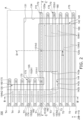
- Embodiments relate to a semiconductor device.
- a semiconductor device such as a MOSFET (Metal-Oxide-Semiconductor Field-Effect Transistor) or the like in which a gate electrode and a FP (Field Plate) electrode are located inside a semiconductor part, an external gate electrode that is electrically connected to the gate electrode inside the semiconductor part and a source electrode that is electrically connected to the FP electrode are located at the surface of the semiconductor part.
- MOSFET Metal-Oxide-Semiconductor Field-Effect Transistor
- a semiconductor device includes: a first electrode; a semiconductor part located on the first electrode; a second electrode located in the semiconductor part, the second electrode extending in a first direction when viewed from above; a third electrode located in the semiconductor part, the third electrode extending in the first direction, the third electrode including a first portion, a second portion, and a first middle portion positioned below the second electrode between the first portion and the second portion, the second electrode being located between the first portion and the second portion in the first direction; a fourth electrode located above the semiconductor part, the fourth electrode including a pad portion separated from the second electrode and the second portion in a second direction crossing the first direction when viewed from above, and a protrusion protruding from the pad portion and covering the second electrode, the protrusion being connected to the second electrode; a fifth electrode located above the semiconductor part and separated from the fourth electrode, the fifth electrode including a first covering portion covering a first contact portion of the semiconductor part adjacent to the second portion when viewed from above, the first covering portion being connected to the
- a semiconductor device includes: a first electrode; a semiconductor part located on the first electrode; a second electrode located in the semiconductor part, the second electrode extending in a first direction when viewed from above; a third electrode, the second electrode including a first end portion in an opposite direction of the first direction, the third electrode including a portion next to the first end portion; a fourth electrode located in the semiconductor part, the fourth electrode being next to the first end portion of the second electrode in a second direction crossing the first direction when viewed from above, the fourth electrode extending in the first direction, a length in the first direction of the fourth electrode being less than a length in the first direction of the second electrode; a fifth electrode, the fourth electrode including a second end portion in the opposite direction of the first direction, the fifth electrode including a portion next to the second end portion in the first direction; a sixth electrode located above the semiconductor part, the sixth electrode being connected to the fourth electrode, the sixth electrode including a pad portion and a protrusion, the pad portion being separated from the second and fourth electrodes
- a semiconductor device includes: a first electrode; a semiconductor part located on the first electrode; a second electrode located in the semiconductor part, the second electrode extending in a first direction when viewed from above; a third electrode located in the semiconductor part, the third electrode extending in the first direction, the third electrode including a first portion, a second portion, and a first middle portion, the second electrode including a first end portion in an opposite direction of the first direction, the first portion being next to the first end portion in the first direction, the second electrode including a second end portion in the first direction, the second portion being next to the second end portion in the first direction, the first middle portion being positioned below the second electrode between the first portion and the second portion; a fourth electrode located in the semiconductor part, the fourth electrode being next to the second electrode in a second direction crossing the first direction when viewed from above, the fourth electrode extending in the first direction; a fifth electrode located in the semiconductor part, the fourth electrode including a third end portion in the opposite direction of the first direction, the fifth electrode including
- an XYZ orthogonal coordinate system An X-axis, a Y-axis, and a Z-axis are orthogonal to each other.
- the direction in which the X-axis extends is taken as an "X-direction"; the direction in which the Y-axis extends is taken as a "Y-direction”; and the direction in which the Z-axis extends is taken as a "Z-direction”.
- the direction of the arrow in the X-direction is taken as the "+X direction”; and the opposite direction is taken as the "-X direction".
- the direction of the arrow in the Y-direction is taken as the "+Y direction”; and the opposite direction is taken as the "-Y direction”. Although the direction of the arrow in the Z-direction is taken as up and the opposite direction is taken as down, these directions are independent of the direction of gravity.
- the notations of the + and - for each conductivity type indicate relative levels of the impurity concentrations of each conductivity type. Specifically, a notation marked with "+” indicates a higher impurity concentration than a notation not marked with either "+” or "-”. A notation marked with "-” indicates a lower impurity concentration than a notation not marked with either "+” or "-”.
- the impurity concentration means the net impurity concentration after the impurities cancel.
- FIG. 6 components that are actually not coplanar are shown as being coplanar to illustrate the positional relationship of the components of the semiconductor device 100 according to the embodiment when viewed from above. Also, for easier understanding of the areas in which a FP electrode 170, a p-type base region 122a, a p + -type contact region 122b, and an n-type source layer 123 that are described below are located in FIG. 6 , the areas in which the FP electrode 170, the p-type base region 122a, the p + -type contact region 122b, and the n-type source layer 123 are located are shown by diagonal hatching.
- the semiconductor device 100 is, for example, a MOSFET. However, it is sufficient for the semiconductor device to include a gate electrode and a FP electrode; and the semiconductor device may be, for example, an IGBT (Insulated Gate Bipolar Transistor).
- IGBT Insulated Gate Bipolar Transistor
- the shape of the semiconductor device 100 when viewed from above is substantially a rectangle of which each side is substantially parallel to the X-direction or the Y-direction.
- the semiconductor device 100 includes a drain electrode 110, a semiconductor part 120, an external gate electrode 130, and a source electrode 140.
- the semiconductor device 100 further includes an insulating film 151, multiple insulating films 152, multiple insulating films 153, and an insulating film 154.
- the semiconductor device further includes multiple internal gate electrodes 160 and multiple FP electrodes 170.
- the components of the semiconductor device 100 will now be described. Hereinbelow, the configuration of a pad portion 131 of the external gate electrode 130 shown in FIG. 1 and the vicinity of the pad portion 131 in the semiconductor device 100 is mainly described, and a description of the other structures is omitted as appropriate.
- the drain electrode 110 is located in substantially the entire region of the lower surface of the semiconductor device 100.
- the upper surface and the lower surface of the drain electrode 110 are flat surfaces that are substantially parallel to the XY plane.
- the drain electrode 110 is made of a conductive material such as a metal material, etc.
- the semiconductor part 120 is located on the drain electrode 110.
- the semiconductor part 120 includes, for example, an n-type semiconductor layer 121, a p-type semiconductor layer 122 that is located in the upper layer portion of the n-type semiconductor layer 121, and the n + -type source layer 123 that is located in the upper layer portion of the p-type semiconductor layer 122.
- the configuration of the semiconductor part can be modified as appropriate according to the type of element.
- the n-type semiconductor layer 121 includes an n - -type drift region.
- the n - -type drift region is located on substantially the entire region of the upper surface of the drain electrode 110.
- the n-type semiconductor layer may further include an n + -type drain region that is located between the n - -type drift region and the drain electrode and includes a higher impurity concentration than the n - -type drift region.
- the p-type semiconductor layer 122 includes the p-type base region 122a, and the p + -type contact region 122b that is located in the p-type base region 122a. As shown in FIG. 5 , the p-type base region 122a is partially provided in the upper layer portion of the n-type semiconductor layer 121. The p + -type contact region 122b is partially provided in the p-type base region 122a and has an ohmic contact with the source electrode 140 that is described below. The details of the arrangement of the p-type base region 122a, the p + -type contact region 122b, and the n + -type source layer 123 are described below.
- the external gate electrode 130 and the source electrode 140 that is separated from the external gate electrode 130 are located above the semiconductor part 120.
- the external gate electrode 130 has a so-called finger configuration.
- the external gate electrode 130 includes, for example, the pad portion 131, a first extension portion 132, multiple second extension portions 133, a third extension portion 134, and a protrusion 135.
- the pad portion 131 is a portion to which a wiring member (not illustrated) is connected to electrically connect the external gate electrode 130 to an external circuit of the semiconductor device 100. According to the embodiment, the pad portion 131 is located at the corner among the four corners of the semiconductor part 120 that is positioned furthest toward the +X side and the +Y side. According to the embodiment, the pad portion 131 is substantially rectangular when viewed from above.
- the first extension portion 132 extends in the -X direction from the corner of the pad portion 131 that is positioned furthest toward the -X side and the +Y side.
- the first extension portion 132 is positioned on the +Y direction end portion of the semiconductor part 120.
- the second extension portions 133 extend in the -Y direction from the first extension portion 132.
- the multiple second extension portions 133 are arranged in the X-direction.
- the third extension portion 134 extends in the -Y direction from the corner of the pad portion 131 that is positioned furthest toward the +X side and the -Y side.
- the -Y direction end portions of each of the second and third extension portions 133 and 134 extend to the vicinity of the -Y direction end portion of the semiconductor part 120.
- the protrusion 135 protrudes in the -Y direction from the -X direction end portion of the pad portion 131, and specifically, the corner positioned furthest toward the -X side and the -Y side.
- the shape of the protrusion 135 when viewed in top-view is, for example, substantially rectangular.
- the length of the protrusion 135 in the Y-direction is less than the lengths of the second and third extension portions 133 and 134 in the Y-direction.
- the external gate electrode 130 is made of a conductive material such as a metal material, etc.
- the external gate electrode 130 may include a stacked body of two or more metal layers.
- the source electrode 140 also has a so-called finger configuration.
- the source electrode 140 includes, for example, multiple first extension portions 141, a second extension portion 142, and multiple third extension portions 143.
- the first extension portions 141 and the second extension portion 142 extend in the +Y direction from the -Y direction end portion of the semiconductor part 120.
- Each first extension portion 141 is positioned between two second extension portions 133 of the external gate electrode 130 that are next to each other.
- the second extension portion 142 is positioned between the second extension portion 133 and the third extension portion 134 that are next to each other.
- Each third extension portion 143 is positioned between the -Y direction end portions of two second extension portions 142 that are next to each other or between the -Y direction end portion of the second extension portion 142 and the -Y direction end portion of the third extension portion 143 that are next to each other; and the third extension portions 143 link these portions to each other.
- the second extension portion 142 includes a first covering portion 142a, a second covering portion 142b, and a third covering portion 142c.
- the third covering portion 142c extends in the +Y direction from the -Y direction end portion of the semiconductor part 120.
- the first covering portion 142a and the second covering portion 142b protrude in the +Y direction from the third covering portion 142c.
- the first covering portion 142a is positioned at the -Y side of the pad portion 131 and the +X side of the protrusion 135.
- the second covering portion 142b is positioned at the -X side of the pad portion 131 and the protrusion 135.
- the protrusion 135 is positioned between the first covering portion 142a and the second covering portion 142b in the X-direction.
- the shapes of the first covering portion 142a, the second covering portion 142b, and the third covering portion 142c when viewed from above are, for example, rectangular.
- a recess 144 is formed from the first covering portion 142a, the second covering portion 142b, and the third covering portion 142c.
- the protrusion 135 is located in the recess 144.
- “the protrusion is located in the recess” means that at least a portion of the protrusion is positioned in the recess.
- the source electrode 140 is made of a conductive material such as a metal material, etc.
- the source electrode 140 may include a stacked body of two or more metal layers.
- a trench T1, two trenches T2, two trenches T3, multiple trenches T4, and multiple trenches T5 are provided in the semiconductor part 120.
- the trenches T1 to T5 extend in the X-direction and are so-called straight-type trenches without branches.
- the trenches T1 to T5 extend downward from the upper surface of the semiconductor part 120.
- the number of the trenches T2 and the number of the trenches T3 are not limited to two and may be one, three, or more.
- a portion of the trench T1 is covered with the second covering portion 142b, the protrusion 135, and the first covering portion 142a when viewed from above.
- the +X direction end portion of the trench T1 is covered with the third extension portion 134 when viewed from above.
- the insulating film 151 is located in the trench T1.
- the insulating film 151 is made of an insulating material such as silicon oxide, silicon nitride, etc.
- the multiple internal gate electrodes 160 and the FP electrode 170 are located in the insulating film 151.
- the internal gate electrode 160 that is positioned furthest toward the +X side among the multiple internal gate electrodes 160 in the trench T1 will now be described.
- the internal gate electrode 160 that is in the trench T1 extends in the X-direction.
- the -X direction end portion of the internal gate electrode 160 is covered with the second covering portion 142b; and the +X direction end portion of the internal gate electrode 160 is covered with the protrusion 135.
- An opening 151hl is provided in the portion of the insulating film 151 positioned between the internal gate electrode 160 and the protrusion 135.
- the protrusion 135 is connected to the internal gate electrode 160 via the opening 151h1.
- the external gate electrode 130 is connected to the internal gate electrode 160 via a current path that extends in the Z-direction.
- the FP electrode 170 that is in the trench T1 extends in the X-direction.
- the FP electrode 170 includes a first portion 171, a second portion 172, and a first middle portion 173 positioned between the first portion 171 and the second portion 172, such that the internal gate electrode 160 is positioned between the first portion 171 and the second portion 172 in the X-direction, and the first middle portion 173 is positioned below the internal gate electrode 160.
- the first portion 171 is positioned at the -X side of the internal gate electrode 160. In other words, the first portion 171 is next to the -X direction end portion of the internal gate electrode 160 in the X-direction.
- the second portion 172 is positioned at the +X side of the internal gate electrode 160, and according to the embodiment, includes the +X direction end portion of the FP electrode 170. In other words, the second portion 172 is next to the +X direction end portion of the internal gate electrode 160 in the X-direction.
- the insulating film 151 is located between the FP electrode 170 and the internal gate electrode 160.
- the FP electrode 170 separates the internal gate electrode 160 from the other internal gate electrode 160 (not illustrated) that is positioned further toward the -X side than the first portion 171 of the FP electrode 170.
- the internal gate electrode 160 thus separated is connected to the protrusion 135. Therefore, the internal gate electrode 160 thus separated can be electrically connected to the external gate electrode 130.
- the first portion 171 is covered with the second covering portion 142b.
- An opening 151h2 is provided in the portion of the insulating film 151 positioned between the first portion 171 and the second covering portion 142b.
- the second covering portion 142b is connected to the first portion 171 via the opening 151h2.
- the -X direction end portion of the second portion 172 is covered with the protrusion 135; and the remaining portion of the second portion 172 is not covered with the protrusion 135 when viewed from above.
- the +X direction end portion of the second portion 172 is covered with the third extension portion 134.
- the portion of the second portion 172 positioned between the two X-direction end portions is covered with the first covering portion 142a.
- An opening 151h3 is provided in the portion of the insulating film 151 positioned between the second portion 172 and the first covering portion 142a.
- the first covering portion 142a is connected to the second portion 172 via the opening 151h3.
- the potential of the second portion 172 extending from the protrusion 135 to the third extension portion 134 when viewed from above easily has the same potential as the source electrode 140.
- the FP electrode 170 is electrically connected to the source electrode 140 via the first portion 171
- the first covering portion 142a may not be connected to the second portion 172 via the opening 151h3 of the insulating film 151.
- the two trenches T2 are positioned at the +Y side of the trench T1 and are arranged in the Y-direction.
- a portion of each trench T2 is covered with the second covering portion 142b; and the +X direction end portion of each trench T2 is covered with the protrusion 135.
- the trenches T2 are not covered with the first covering portion 142a.
- the insulating film 152 is located in each trench T2.
- the insulating films 152 are made of an insulating material such as silicon oxide, silicon nitride, etc.
- the multiple internal gate electrodes 160 and the FP electrode 170 are located in each insulating film 152.
- the internal gate electrode 160 that is positioned furthest toward the +X side among the multiple internal gate electrodes 160 in each trench T2 will now be described.
- the internal gate electrode 160 that is in each trench T2 extends in the X-direction.
- the -X direction end portion of this internal gate electrode 160 is covered with the second covering portion 142b; and the +X direction end portion of this internal gate electrode 160 is covered with the protrusion 135.
- An opening 152h1 is provided in the portion of the insulating film 152 positioned between this internal gate electrode 160 and the protrusion 135.
- the protrusion 135 is connected to this internal gate electrode 160 via the opening 152h1.
- the FP electrode 170 that is in each trench T2 extends in the X-direction.
- the FP electrode 170 includes a third portion 174, a fourth portion 175, and a second middle portion 176 positioned between the third portion 174 and the fourth portion 175, such that the internal gate electrode 160 is positioned between the third portion 174 and the fourth portion 175 in the X-direction, and the second middle portion 176 is positioned below the internal gate electrode 160.
- the third portion 174 is positioned at the -X side of the internal gate electrode 160. In other words, the third portion 174 is next to the -X direction end portion of the internal gate electrode 160 in the X-direction.
- the third portion 174 is next to the first portion 171 in the Y-direction.
- the fourth portion 175 is positioned at the +X side of the internal gate electrode 160, and according to the embodiment, corresponds to the +X direction end portion of the FP electrode 170. In other words, the fourth portion 175 is next to the +X direction end portion of the internal gate electrode 160 in the X-direction.
- the insulating film 152 is located between the internal gate electrode 160 and the FP electrode 170.
- the FP electrode 170 separates the internal gate electrode 160 from the other internal gate electrode 160 (not illustrated) that is positioned further toward the -X side than the third portion 174 of the FP electrode 170.
- the internal gate electrode 160 thus separated is connected to the protrusion 135. Therefore, the internal gate electrode 160 thus separated can be electrically connected to the external gate electrode 130.
- the third portion 174 is covered with the second covering portion 142b.
- An opening 152h2 is provided in the portion of the insulating film 152 positioned between the third portion 174 and the second covering portion 142b.
- the second covering portion 142b is connected to the third portion 174 via the opening 152h2.
- the fourth portion 175 is covered with the protrusion 135.
- the length in the X-direction of the fourth portion 175 is less than the length in the X-direction of the second portion 172.
- the pad portion 131 is separated from the +X direction end portion of the internal gate electrode 160 in each trench T2.
- a distance L between the first covering portion 142a and the pad portion 131 in the Y-direction is greater than distances L1 and L2 between the pad portion 131 and the trenches T2 in the Y-direction.
- the positions of the trenches T2 in the Y-direction are between the position of the pad portion 131 in the Y-direction and the position of the first covering portion 142a in the Y-direction.
- the protrusion 135 protrudes from the pad portion 131, covers the +X direction end portion of the internal gate electrode 160 in each trench T2, and is connected to the +X direction end portion of the internal gate electrode 160 in each trench T2.
- the two trenches T3 are positioned at the -Y side of the trench T1 in the Y-direction.
- a portion of each trench T3 is covered with the first and second covering portions 142a and 142b and not covered with the protrusion 135.
- the +X direction end portion of each trench T3 is covered with the third extension portion 134 when viewed from above.
- the insulating film 153 is located in each trench T3.
- the insulating films 153 are made of an insulating material such as silicon oxide, silicon nitride, etc.
- the multiple internal gate electrodes 160 and the FP electrode 170 are located in each insulating film 153.
- the internal gate electrode 160 that is positioned furthest toward the +X side among the multiple internal gate electrodes 160 in each trench T3 will now be described.
- the internal gate electrode 160 that is in each trench T3 extends in the X-direction.
- the -X direction end portion of this internal gate electrode 160 is covered with the second covering portion 142b; and the +X direction end portion of this internal gate electrode 160 is covered with the third extension portion 134.
- the first covering portion 142a covers between the two X-direction end portions of this internal gate electrode 160.
- An opening 153h1 is provided in the portion of the insulating film 153 positioned between this internal gate electrode 160 and the third extension portion 134.
- the third extension portion 134 is connected to this internal gate electrode 160 via the opening 153h1.
- the FP electrode 170 that is in each trench T3 extends in the X-direction.
- the FP electrode 170 includes a fifth portion 177, a sixth portion 178, and a third middle portion 179 between the fifth portion 177 and the sixth portion 178, such that the internal gate electrode 160 is positioned between the fifth portion 177 and the sixth portion 178 in the X-direction, and the third middle portion 179 is positioned below the internal gate electrode 160.
- the fifth portion 177 is positioned at the -X side of the internal gate electrode 160. In other words, the fifth portion 177 is next to the -X direction end portion of the internal gate electrode 160 in the X-direction.
- the fifth portion 177 is next to the first portion 171 in the Y-direction.
- the sixth portion 178 is positioned at the +X side of the internal gate electrode 160, and according to the embodiment, corresponds to the +X direction end portion of the FP electrode 170. In other words, the sixth portion 178 is next to the +X direction end portion of the internal gate electrode 160 in the X-direction.
- the insulating film 153 is located between the internal gate electrode 160 and the FP electrode 170.
- the FP electrode 170 separates the internal gate electrode 160 from the other internal gate electrode 160 (not illustrated) that is positioned further toward the -X side than the fifth portion 177 of the FP electrode 170.
- the internal gate electrode 160 thus separated is connected to the third extension portion 134. Therefore, the internal gate electrode 160 thus separated can be electrically connected to the external gate electrode 130.
- the fifth portion 177 is covered with the second covering portion 142b.
- An opening 153h2 is provided in the portion of the insulating film 153 positioned between the fifth portion 177 and the second covering portion 142b.
- the second covering portion 142b is connected to the fifth portion 177 via the opening 153h2.
- the sixth portion 178 is covered with the third extension portion 134.
- the length in the X-direction of the sixth portion 178 is less than the length in the X-direction of the second portion 172.
- the multiple trenches T4 are located at the +Y side of the multiple trenches T2 and are arranged in the Y-direction.
- the configuration and the internal configuration of each trench T4 are substantially similar to those of the trench T2; and a description is therefore omitted.
- the multiple trenches T5 are located at the +Y side of the multiple trenches T3 and are arranged in the Y-direction.
- the configuration and the internal configuration of each trench T5 are substantially similar to those of the trench T3; and a description is therefore omitted.
- the insulating film 154 is located between the external gate electrode 130 and the upper surface of the semiconductor part 120 and between the source electrode 140 and the upper surface of the semiconductor part 120.
- three openings 154h1, multiple openings 154h2, and multiple openings 154h3 are provided in the insulating film 154.
- Each opening 154h1 is positioned between the first covering portion 142a of the source electrode 140 and a contact portion 120a positioned between the trenches T1, T3, and T5 that are next to each other in the semiconductor part 120.
- the openings 154h1 extend in the X-direction and are covered with the first covering portion 142a when viewed from above.
- the first covering portion 142a is connected to the contact portions 120a via the openings 154h1.
- the contact portion 120a is the surface of a trench T6 that extends downward from the upper surface of the semiconductor part 120. This is similar for the other contact portions 120b and 120c that are described below as well.
- a portion of the upper surface of the semiconductor part may be used as a contact portion without providing such a trench in the semiconductor part.
- the p-type base region 122a and the p + -type contact region 122b are included but the n-type source layer 123 is not included in the contact portion 120a between the trench T1 and the trench T3 that are next to each other and in the contact portion 120a between the trenches T3 that are next to each other.
- the n-type source layer 123 also may be included in the contact portion 120a.
- the p-type base region 122a, the p + -type contact region 122b, and the n-type source layer 123 are included in the contact portion 120a between the trench T3 and the trench T5 that are next to each other.
- each opening 154h2 is positioned between the second covering portion 142b of the source electrode 140 and the contact portion 120b positioned between the trenches T1, T2, and T4 that are next to each other in the semiconductor part 120.
- the openings 154h2 extend in the X-direction.
- the second covering portion 142b is connected to the contact portions 120b via the openings 154h2.
- the p-type base region 122a, the p + -type contact region 122b, and the n-type source layer 123 are included in each contact portion 120b.
- each opening 154h3 is positioned between the third covering portion 142c and the contact portion 120c positioned between the trenches T5 that are next to each other in the semiconductor part 120.
- the openings 154h3 extend in the X-direction.
- the third covering portion 142c is connected to the contact portions 120c via the openings 154h3.
- the p-type base region 122a, the p + -type contact region 122b, and the n-type source layer 123 are included in each contact portion 120c.
- FIG. 7 is an enlarged schematic view showing the positional relationship of components of a semiconductor device according to a reference example when viewed from above.
- the protrusion 135 that protrudes in the -Y direction from the pad portion 131 is not included in an external gate electrode 930. Also, in the semiconductor device 900 according to the reference example, the recess 144 in which the protrusion 135 is located is not provided in a source electrode 940.
- the distance L is the length between two trenches arranged in the Y-direction.
- the vicinity of the pad portion 131 is the termination region of the semiconductor device 900. Therefore, from the perspective of increasing the breakdown voltage, it is favorable for the FP electrode 170 to extend to the +X direction end portion of each of the trenches T1 to T6, and for the internal gate electrode 160 not to be provided in the end portion of each of the trenches T1 to T6. Thus, when the FP electrode 170 extends to the +X direction end portion of each of the trenches T1 to T6, even if the internal gate electrode 160 is located at the vicinity of the pad portion 131 in each of the trenches T1 to T6, the FP electrode 170 separates this internal gate electrode 160 from the internal gate electrode 160 at the center of the semiconductor part 120. Accordingly, in the semiconductor device 900 according to the reference example, it is necessary to connect such an internal gate electrode 160 to the pad portion 131 or the third extension portion 134.
- the semiconductor device 900 even if the two trenches T2 extend to be directly under the third extension portion 134, the internal gate electrodes 160 are provided inside the two trenches T2, and the third extension portion 134 is connected to these internal gate electrodes 160, the source electrode 940 cannot be connected to the portion of the semiconductor part 120 positioned between the pad portion 131 and the source electrode 940 in the Y-direction. Therefore, there is a possibility that the gate capacity and the avalanche resistance may decrease.
- the semiconductor device 900 it is favorable to provide the FP electrodes 170 in the +X direction end portions of the two trenches T2 and cover the FP electrodes 170 with the source electrode 140 without the two trenches T2 extending to the third extension portion 134 so that the gate capacity and/or the avalanche resistance does not decrease.
- the trench T1 and the portion of the trench T4 that is positioned furthest toward the -Y side and is not positioned between two other trenches are end point regions; therefore, it is favorable to provide the FP electrode 170 from the perspective of increasing the breakdown voltage. Accordingly, in the semiconductor device 900 according to the reference example, the region between the trench T1 and the trench T4 positioned furthest toward the -Y side is ineffective as an element such as a MOSFET, etc.
- the external gate electrode 130 includes the protrusion 135 that protrudes from the pad portion 131, covers the internal gate electrode 160 in the trench T1, and is connected to the internal gate electrode 160.
- the source electrode 140 includes the first covering portion 142a that covers the contact portion 120a of the semiconductor part 120 adjacent to the second portion 172 of the FP electrode in the trench T1 when viewed from above and is connected to the contact portion 120a, and includes the second covering portion 142b that covers the first portion 171 and is connected to the contact portion 120a.
- the internal gate electrode 160 can be located in the trench T1 and connected to the external gate electrode 130 at the vicinity of the pad portion 131 while maintaining the state in which the FP electrode in the trench T1 and the contact portion 120a of the semiconductor part 120 are connected to the source electrode 140. Therefore, the effective element area can be increased.
- the first covering portion 142a also covers the second portion 172 of the FP electrode 170 in the trench T1 and is connected to the second portion 172. Therefore, the potential of the second portion 172 can easily be the same potential as the potential of the source electrode 140.
- the internal gate electrode 160 that is in each trench T2 positioned in the Y-direction between the position of the pad portion 131 in the Y-direction and the position of the first covering portion 142a in the Y-direction cannot be directly connected to the pad portion 131.
- the protrusion 135 covers the internal gate electrode 160 in the trench T2 when viewed from above and is connected to the internal gate electrode 160. Therefore, the effective element area can be increased.
- the second covering portion 142b covers the contact portion 120b of the semiconductor part 120 positioned between the internal gate electrode 160 in the trench T1 and the internal gate electrode 160 in the trench T2 when viewed from above, and is connected to the contact portion 120b. Therefore, the effective element area can be increased.
- the n-type source layer 123 is included in the contact portion 120b. Therefore, the surface area in which the n-type source layer 123 is located can be increased.
- the n-type source layer 123 also is located under the first covering portion 142a; and the first covering portion 142a is connected to the n-type source layer 123. Therefore, the surface area in which the n-type source layer 123 is located can be increased.
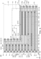
- FIG. 8 is a top view showing a semiconductor device according to the embodiment.
- FIG. 9 is a schematic view showing the positional relationship of components when viewed from above in the portion surrounded with broken line E of FIG. 8 .
- the semiconductor device 200 according to the embodiment differs from the semiconductor device 100 according to the first embodiment in that a pad portion 231 is positioned at substantially the X-direction center of the semiconductor part 120.
- An external gate electrode 230 includes the pad portion 231, a first extension portion 232, a second extension portion 233, a third extension portion 234, a fourth extension portion 235, a fifth extension portion 236, and two protrusions 237.
- the pad portion 231 is positioned at substantially the X-direction center at the +Y direction end portion of the semiconductor part 120.
- the shape of the pad portion 231 when viewed from above is substantially rectangular.
- the position of the pad portion is not limited to a corner of the semiconductor part.
- the first extension portion 232 extends in the -X direction from the corner of the pad portion 231 positioned furthest toward the -X side and the +Y side.
- the second extension portion 233 extends in the +X direction from the corner of the pad portion 231 positioned furthest toward the +X side and the +Y side.
- the third extension portion 234 extends in the -Y direction from the -X direction end portion of the first extension portion 232.
- the fourth extension portion 235 extends in the -Y direction from substantially the X-direction center at the +Y direction end portion of the pad portion 231.
- the fifth extension portion 236 extends in the -Y direction from the +X direction end portion of the second extension portion 233.
- protrusion 237 protrudes in the -Y direction from the -X direction end portion of the pad portion 231, and specifically, the corner positioned furthest toward the -X side and the -Y side.
- Another protrusion 237 protrudes in the -Y direction from the +X direction end portion of the pad portion 231, and specifically, the end portion positioned furthest toward the +X side and the -Y side.
- a source electrode 240 includes a first extension portion 241, a second extension portion 242, and a third extension portion 243.
- the first extension portion 241 extends in the +Y direction from the -Y direction end portion of the semiconductor part 120 and is positioned between the third extension portion 234 and the fourth extension portion 235 of the external gate electrode 230.
- the second extension portion 242 extends in the +Y direction from the -Y direction end portion of the semiconductor part 120 and is positioned between the fourth extension portion 235 and the fifth extension portion 236 of the external gate electrode 230.
- the third extension portion 243 is positioned between the -Y direction end portion of the first extension portion 241 and the -Y direction end portion of the second extension portion 242 and is linked to these end portions.
- the first extension portion 241 includes a first covering portion 241a, a second covering portion 241b, and a third covering portion 241c.
- the third covering portion 241c extends in the +Y direction from the -Y direction end portion of the semiconductor part 120.
- the first covering portion 241a and the second covering portion 241b protrude in the +Y direction from the third covering portion 241c.
- the first covering portion 241a is positioned at the -Y side of the pad portion 231 and the +X side of the protrusion 237.
- the second covering portion 241b is positioned at the -X side of the pad portion 231 and the protrusion 237.
- One protrusion 237 is positioned between the first covering portion 241a and the second covering portion 241b in the X-direction.
- a recess 244 is formed from the first covering portion 241a, the second covering portion 241b, and the third covering portion 241c.
- the protrusion 237 is located in the recess 244.
- the shape of the second extension portion 242 is substantially symmetric with the first extension portion 241 with respect to a central axis C of the semiconductor device 200 extending in the Y-direction; and a description is therefore omitted.
- the structure of the vicinity of the pad portion 231 at the -X side of the central axis C will now be described.
- the structure of the vicinity of the pad portion 231 at the +X side of the central axis C is symmetric with the structure of the vicinity of the pad portion 231 at the -X side of the central axis C when referenced to the central axis C; and a description is therefore omitted.
- a trench T21, two trenches T22, two trenches T23, multiple trenches T24, and multiple trenches T25 are provided in the semiconductor part 120.
- the structure and the internal structure of the trench T21 are similar to those of the trench T1 according to the first embodiment; and a description is therefore omitted.
- the structure and the internal structure of the trench T22 are similar to those of the trench T2 according to the first embodiment; and a description is therefore omitted.
- the structure and the internal structure of the trench T23 are similar to those of the trench T3 according to the first embodiment; and a description is therefore omitted.
- the structure and the internal structure of the trench T24 are similar to those of the trench T4 according to the first embodiment; and a description is therefore omitted.
- the structure and the internal structure of the trench T25 are similar to those of the trench T5 according to the first embodiment; and a description is therefore omitted.
- the protrusion 237 covers the internal gate electrode 160 in the trench T21 and the internal gate electrode 160 in the trench T22 when viewed from above and is connected to these internal gate electrodes via the openings 151h1 and 152h1.
- the fourth extension portion 235 covers the internal gate electrodes 160 in the trenches T23 and T25 and is connected to these internal gate electrodes via the openings 153h1.
- the first covering portion 241a covers the second portion 172 of the FP electrode 170 in the trench T21 when viewed from above and is connected to the second portion via the opening 151h3.
- the first covering portion 241a covers the contact portions 120a between the trenches T21 and T23 that are next to each other in the semiconductor part 120, and is connected to these contact portions via the openings 154h1.
- the second covering portion 241b covers the first portion 171 of the FP electrode 170 in the trench T21, the third portions 174 of the FP electrodes 170 in the trenches T22 and T24, and the FP electrodes 170 in the trenches T23 and T25, and is connected to these FP electrodes via the openings 151h2, 152h2, and 153h2.
- the second covering portion 241b covers the contact portions 120b between the trenches T21, T22, and T24 that are next to each other in the semiconductor part 120, and is connected to these contact portions via the openings 154h2.
- the third covering portion 241c covers the FP electrodes 170 in the trenches T25 when viewed from above and is connected to these FP electrodes via the openings 153h2. When viewed from above, the third covering portion 241c covers the contact portions 120c between the trenches T23 and T25 that are next to each other in the semiconductor part 120, and is connected to these contact portions via the openings 154h3.
- the external gate electrode 230 includes the protrusion 237 that protrudes from the pad portion 231, covers the internal gate electrode 160 in the trench T21, and is connected to the internal gate electrode 160.
- the source electrode 240 includes the first covering portion 241a that covers the contact portion 120a of the semiconductor part 120 adjacent to the second portion 172 of the FP electrode in the trench T21 when viewed from above and is connected to the second portion 172, and includes the second covering portion 241b that covers the first portion 171 and is connected to the first portion 171.
- the internal gate electrode 160 can be connected to the external gate electrode 230 in the trench T21 while maintaining the state in which the FP electrode 170 in the trench T21 and the contact portion 120a of the semiconductor part 120 are connected to the source electrode 240. Therefore, the effective element area can be increased.
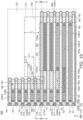
- FIG. 10 is a schematic view showing the positional relationship of components of the semiconductor device according to the embodiment when viewed from above.
- FIG. 11 is a cross-sectional view along line F-F' of FIG. 10 .
- FIG. 12 is a cross-sectional view along line G-G' of FIG. 10 .
- the internal structures of the trenches T1, T2, T3, T4, and T5 of the semiconductor device 300 according to the embodiment are different from those of the semiconductor device 100 according to the first embodiment.
- the internal gate electrode 160 that is in the trench T1 extends to a position that overlaps the third extension portion 134 when viewed from above.
- the +X direction end portion of this internal gate electrode 160 overlaps the third extension portion 134.
- the contact portion 120a is adjacent to this internal gate electrode 160.
- the length in the X-direction of the internal gate electrode 160 in the trench T2 is less than the length in the X-direction of the internal gate electrode 160 in the trench T1.
- the protrusion 135 overlaps a portion of this internal gate electrode 160 between the two X-direction end portions when viewed from above.
- the protrusion 135 is connected to the portion of this internal gate electrode 160 between the two X-direction end portions via an opening 151h in the insulating film 151 in the trench T1.
- this internal gate electrode 160 may be connected to the third extension portion 134 instead of the protrusion 135.
- the protrusion 135 may not cover the trench T1.
- the protrusion 135 may be separated from the trench T1 in the +Y direction when viewed from above.
- This internal gate electrode 160 may be connected to both the protrusion 135 and the third extension portion 134.
- the FP electrode 170 that is in the trench T1 includes a portion 371 that is next to the -X direction end portion of the internal gate electrode 160 in the -X direction, and a portion 372 that is linked to the +X direction end portion of the portion 371 and is located below the internal gate electrode 160.
- the internal gate electrode 160 is located in the portion of the trench T1 that is positioned in the termination region.
- the internal gate electrode 160 may be located in the termination region according to the thickness of the termination region of the insulating film 151 and/or the breakdown voltage of the semiconductor device 100. This is similar for the other trenches T2 to T5 described below as well.
- the FP electrode 170 that is in the trench T2 includes a portion 373 that is next to the -X direction end portion of the internal gate electrode 160 in the -X direction, and a portion 374 that is linked to the +X direction end portion of the portion 373 and is located below the internal gate electrode 160.
- the portion 373 is next to the portion 371 of the FP electrode 170 in the trench T1 in the Y-direction.
- the internal gate electrode 160 is located also in the portion of the trench T2 that is positioned in the termination region.
- the arrangement of the FP electrode 170 in the trench T4 is similar to the arrangement of the FP electrode 170 in the trench T2.
- the arrangements of the FP electrodes 170 in the trenches T3 and T5 are similar to the arrangement of the FP electrode 170 in the trench T1. Accordingly, a description of the internal configurations of the trenches T3, T4, and T5 is omitted.
- the pad portion 131 is separated in the +Y direction from the +X direction end portion of the internal gate electrode 160 in each trench T2.
- the distance L between the first covering portion 142a and the pad portion 131 in the Y-direction is greater than the distances L1 and L2 between the pad portion 131 and the trenches T2 in the Y-direction.
- the protrusion 135 protrudes from the pad portion 131, covers the +X direction end portion of the internal gate electrode 160 in each trench T2, and is connected to the +X direction end portion of the internal gate electrode 160 in each trench T2.
- the internal gate electrode 160 that is in each trench T2 and is positioned in the Y-direction between the position of the pad portion 131 in the Y-direction and the position of the first covering portion 142a in the Y-direction is not easily connected directly to the pad portion 131.
- such an internal gate electrode 160 can be electrically connected to the external gate electrode 130 by the protrusion 135.
- the second covering portion 142b covers the contact portion 120b of the semiconductor part 120 between the internal gate electrode 160 in the trench T1 and the internal gate electrode 160 in the trench T2 positioned furthest toward the -Y side, and is connected to the contact portion 120b. Therefore, the effective element area can be increased.
- the first covering portion 142a covers the contact portion 120a of the semiconductor part 120 adjacent to the internal gate electrode 160 in the trench T1, and is connected to the contact portion 120a. Therefore, the effective element area can be increased.
- Embodiments may include the following configurations (e.g., technological proposals).
- a semiconductor device comprising:
- a semiconductor device comprising:
- a semiconductor device comprising:
Landscapes
- Electrodes Of Semiconductors (AREA)
Abstract
A semiconductor device includes: a second electrode, located in a semiconductor part, extending in a first direction; a third electrode, located in the semiconductor part, including a first portion, a second portion, and a first middle portion positioned below the second electrode between the first portion and the second portion, the second electrode being located between the first portion and the second portion in the first direction; a fourth electrode, located above the semiconductor part, including a pad portion separated from the second electrode and the second portion in a second direction, and a protrusion protruding from the pad portion and covering the second electrode and being connected to the second electrode; and a fifth electrode, located above the semiconductor part, including a first covering portion being connected to the first contact portion and a second covering portion being connected to the first portion.
Description
- Embodiments relate to a semiconductor device.
- In a conventionally known structure of a semiconductor device such as a MOSFET (Metal-Oxide-Semiconductor Field-Effect Transistor) or the like in which a gate electrode and a FP (Field Plate) electrode are located inside a semiconductor part, an external gate electrode that is electrically connected to the gate electrode inside the semiconductor part and a source electrode that is electrically connected to the FP electrode are located at the surface of the semiconductor part.
-
-
FIG. 1 is a top view showing a semiconductor device according to a first embodiment; -
FIG. 2 is an enlarged top view of a portion ofFIG. 1 surrounded with broken line A; -
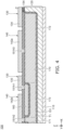
FIG. 3 is a cross-sectional view along line B-B' ofFIG. 2 ; -
FIG. 4 is a cross-sectional view along line C-C' ofFIG. 2 ; -
FIG. 5 is a cross-sectional view along line D-D' ofFIG. 2 ; -
FIG. 6 is a schematic view showing a positional relationship of components of the semiconductor device according to the first embodiment when viewed from above; -
FIG. 7 is an enlarged schematic view showing the positional relationship of components of a semiconductor device according to a reference example when viewed from above; -
FIG. 8 is a top view showing a semiconductor device according to a second embodiment; -
FIG. 9 is a schematic view showing a positional relationship of components when viewed from above in the portion surrounded with broken line E ofFIG. 8 ; -
FIG. 10 is a schematic view showing a positional relationship of components of a semiconductor device according to a third embodiment when viewed from above; -
FIG. 11 is a cross-sectional view along line F-F' ofFIG. 10 ; and -
FIG. 12 is a cross-sectional view along line G-G' of FIG. - In general, according to one embodiment, a semiconductor device includes: a first electrode; a semiconductor part located on the first electrode; a second electrode located in the semiconductor part, the second electrode extending in a first direction when viewed from above; a third electrode located in the semiconductor part, the third electrode extending in the first direction, the third electrode including a first portion, a second portion, and a first middle portion positioned below the second electrode between the first portion and the second portion, the second electrode being located between the first portion and the second portion in the first direction; a fourth electrode located above the semiconductor part, the fourth electrode including a pad portion separated from the second electrode and the second portion in a second direction crossing the first direction when viewed from above, and a protrusion protruding from the pad portion and covering the second electrode, the protrusion being connected to the second electrode; a fifth electrode located above the semiconductor part and separated from the fourth electrode, the fifth electrode including a first covering portion covering a first contact portion of the semiconductor part adjacent to the second portion when viewed from above, the first covering portion being connected to the first contact portion, and a second covering portion covering the first portion, the second covering portion being connected to the first portion; and a first insulating film located between the semiconductor part and the second electrode, between the semiconductor part and the third electrode, and between the second electrode and the third electrode.
- In general, according to one embodiment, a semiconductor device includes: a first electrode; a semiconductor part located on the first electrode; a second electrode located in the semiconductor part, the second electrode extending in a first direction when viewed from above; a third electrode, the second electrode including a first end portion in an opposite direction of the first direction, the third electrode including a portion next to the first end portion; a fourth electrode located in the semiconductor part, the fourth electrode being next to the first end portion of the second electrode in a second direction crossing the first direction when viewed from above, the fourth electrode extending in the first direction, a length in the first direction of the fourth electrode being less than a length in the first direction of the second electrode; a fifth electrode, the fourth electrode including a second end portion in the opposite direction of the first direction, the fifth electrode including a portion next to the second end portion in the first direction; a sixth electrode located above the semiconductor part, the sixth electrode being connected to the fourth electrode, the sixth electrode including a pad portion and a protrusion, the pad portion being separated from the second and fourth electrodes in the second direction, the protrusion protruding from the pad portion, the fourth electrode including a third end portion in the first direction, the protrusion covering the third end portion, the protrusion being connected to the third end portion; and a seventh electrode located above the semiconductor part, the seventh electrode being separated from the pad portion in an opposite direction of the second direction, the seventh electrode including a first covering portion and a second covering portion, a distance from the pad portion to the first covering portion in the second direction being greater than a distance between the fourth electrode and the pad portion in the second direction, the second covering portion covering the portion of the third electrode, the portion of the fifth electrode, and a first contact portion of the semiconductor part, the first contact portion being positioned between the second electrode and the fourth electrode, the second covering portion being connected to the portion of the third electrode, the portion of the fifth electrode, and the first contact portion; a first insulating film located between the semiconductor part and the second electrode, between the semiconductor part and the third electrode, and between the second electrode and the third electrode; and a second insulating film located between the semiconductor part and the fourth electrode, between the semiconductor part and the fifth electrode, and between the fourth electrode and the fifth electrode.
- In general, according to one embodiment, a semiconductor device includes: a first electrode; a semiconductor part located on the first electrode; a second electrode located in the semiconductor part, the second electrode extending in a first direction when viewed from above; a third electrode located in the semiconductor part, the third electrode extending in the first direction, the third electrode including a first portion, a second portion, and a first middle portion, the second electrode including a first end portion in an opposite direction of the first direction, the first portion being next to the first end portion in the first direction, the second electrode including a second end portion in the first direction, the second portion being next to the second end portion in the first direction, the first middle portion being positioned below the second electrode between the first portion and the second portion; a fourth electrode located in the semiconductor part, the fourth electrode being next to the second electrode in a second direction crossing the first direction when viewed from above, the fourth electrode extending in the first direction; a fifth electrode located in the semiconductor part, the fourth electrode including a third end portion in the opposite direction of the first direction, the fifth electrode including a third portion that is next to the third end portion in the first direction; a sixth electrode located above the semiconductor part, the sixth electrode including a pad portion and a protrusion, the pad portion being separated in the second direction from the second and fourth electrodes, the protrusion protruding from the pad portion, the fourth electrode including a fourth end portion in the first direction, the protrusion covering the second end portion of the second electrode and the fourth end portion of the fourth electrode, the protrusion being connected to the second and fourth end portions, the protrusion not covering at least a portion of the second portion when viewed from above; a seventh electrode located above the semiconductor part and separated from the pad portion in an opposite direction of the second direction, the seventh electrode including a first covering portion and a second covering portion, a distance from the pad portion to the first covering portion in the second direction being greater than a distance between the fourth electrode and the pad portion in the second direction, the second covering portion covering the first portion, the third portion, and a first contact portion of the semiconductor part positioned between the second electrode and the fourth electrode, the second covering portion being connected to the first portion, the third portion, and the first contact portion; a first insulating film located between the semiconductor part and the second electrode, between the semiconductor part and the third electrode, and between the second electrode and the third electrode; and a second insulating film located between the semiconductor part and the fourth electrode, between the semiconductor part and the fifth electrode, and between the fourth electrode and the fifth electrode.
- Exemplary embodiments will now be described with reference to the drawings. The drawings are schematic or conceptual; and the relationships between the thickness and width of portions, the proportional coefficients of sizes among portions, etc., are not necessarily the same as the actual values thereof. Furthermore, the dimensions and proportional coefficients may be illustrated differently among drawings, even for identical portions. In the specification of the application and the drawings, components similar to those described in regard to a drawing thereinabove are marked with like reference numerals, and a detailed description is omitted as appropriate.
- For easier understanding of the following description, the arrangements and configurations of the portions are described using an XYZ orthogonal coordinate system. An X-axis, a Y-axis, and a Z-axis are orthogonal to each other. The direction in which the X-axis extends is taken as an "X-direction"; the direction in which the Y-axis extends is taken as a "Y-direction"; and the direction in which the Z-axis extends is taken as a "Z-direction". The direction of the arrow in the X-direction is taken as the "+X direction"; and the opposite direction is taken as the "-X direction". The direction of the arrow in the Y-direction is taken as the "+Y direction"; and the opposite direction is taken as the "-Y direction". Although the direction of the arrow in the Z-direction is taken as up and the opposite direction is taken as down, these directions are independent of the direction of gravity.
- Hereinbelow, the notations of the + and - for each conductivity type indicate relative levels of the impurity concentrations of each conductivity type. Specifically, a notation marked with "+" indicates a higher impurity concentration than a notation not marked with either "+" or "-". A notation marked with "-" indicates a lower impurity concentration than a notation not marked with either "+" or "-". Here, when both an impurity that forms donors and an impurity that forms acceptors are included in each region, the "impurity concentration" means the net impurity concentration after the impurities cancel.
- First, a first embodiment will be described.
-
FIG. 1 is a top view showing a semiconductor device according to the embodiment. -
FIG. 2 is an enlarged top view of a portion ofFIG. 1 surrounded with broken line A. -
FIG. 3 is a cross-sectional view along line B-B' ofFIG. 2 . -
FIG. 4 is a cross-sectional view along line C-C' ofFIG. 2 . -
FIG. 5 is a cross-sectional view along line D-D' ofFIG. 2 . -
FIG. 6 is a schematic view showing the positional relationship of the components of the semiconductor device according to the embodiment when viewed from above. - In
FIG. 6 , components that are actually not coplanar are shown as being coplanar to illustrate the positional relationship of the components of thesemiconductor device 100 according to the embodiment when viewed from above. Also, for easier understanding of the areas in which aFP electrode 170, a p-type base region 122a, a p+-type contact region 122b, and an n-type source layer 123 that are described below are located inFIG. 6 , the areas in which theFP electrode 170, the p-type base region 122a, the p+-type contact region 122b, and the n-type source layer 123 are located are shown by diagonal hatching. - The
semiconductor device 100 according to the embodiment is, for example, a MOSFET. However, it is sufficient for the semiconductor device to include a gate electrode and a FP electrode; and the semiconductor device may be, for example, an IGBT (Insulated Gate Bipolar Transistor). - As shown in
FIG. 1 , the shape of thesemiconductor device 100 when viewed from above is substantially a rectangle of which each side is substantially parallel to the X-direction or the Y-direction. However, the shape of the semiconductor device is not limited to that described above. Generally speaking, as shown inFIGS. 2 and3 , thesemiconductor device 100 includes adrain electrode 110, asemiconductor part 120, anexternal gate electrode 130, and asource electrode 140. Thesemiconductor device 100 further includes aninsulating film 151, multipleinsulating films 152, multipleinsulating films 153, and aninsulating film 154. The semiconductor device further includes multipleinternal gate electrodes 160 andmultiple FP electrodes 170. The components of thesemiconductor device 100 will now be described. Hereinbelow, the configuration of apad portion 131 of theexternal gate electrode 130 shown inFIG. 1 and the vicinity of thepad portion 131 in thesemiconductor device 100 is mainly described, and a description of the other structures is omitted as appropriate. - The
drain electrode 110 is located in substantially the entire region of the lower surface of thesemiconductor device 100. For example, as shown inFIG. 3 , the upper surface and the lower surface of thedrain electrode 110 are flat surfaces that are substantially parallel to the XY plane. Thedrain electrode 110 is made of a conductive material such as a metal material, etc. Thesemiconductor part 120 is located on thedrain electrode 110. - The
semiconductor part 120 includes, for example, an n-type semiconductor layer 121, a p-type semiconductor layer 122 that is located in the upper layer portion of the n-type semiconductor layer 121, and the n+-type source layer 123 that is located in the upper layer portion of the p-type semiconductor layer 122. However, the configuration of the semiconductor part can be modified as appropriate according to the type of element. - The n-
type semiconductor layer 121 includes an n--type drift region. The n--type drift region is located on substantially the entire region of the upper surface of thedrain electrode 110. However, the n-type semiconductor layer may further include an n+-type drain region that is located between the n--type drift region and the drain electrode and includes a higher impurity concentration than the n--type drift region. - The p-
type semiconductor layer 122 includes the p-type base region 122a, and the p+-type contact region 122b that is located in the p-type base region 122a. As shown inFIG. 5 , the p-type base region 122a is partially provided in the upper layer portion of the n-type semiconductor layer 121. The p+-type contact region 122b is partially provided in the p-type base region 122a and has an ohmic contact with thesource electrode 140 that is described below. The details of the arrangement of the p-type base region 122a, the p+-type contact region 122b, and the n+-type source layer 123 are described below. - As shown in
FIG. 1 , theexternal gate electrode 130 and thesource electrode 140 that is separated from theexternal gate electrode 130 are located above thesemiconductor part 120. - The
external gate electrode 130 has a so-called finger configuration. Theexternal gate electrode 130 includes, for example, thepad portion 131, afirst extension portion 132, multiplesecond extension portions 133, athird extension portion 134, and aprotrusion 135. - The
pad portion 131 is a portion to which a wiring member (not illustrated) is connected to electrically connect theexternal gate electrode 130 to an external circuit of thesemiconductor device 100. According to the embodiment, thepad portion 131 is located at the corner among the four corners of thesemiconductor part 120 that is positioned furthest toward the +X side and the +Y side. According to the embodiment, thepad portion 131 is substantially rectangular when viewed from above. - The
first extension portion 132 extends in the -X direction from the corner of thepad portion 131 that is positioned furthest toward the -X side and the +Y side. Thefirst extension portion 132 is positioned on the +Y direction end portion of thesemiconductor part 120. Thesecond extension portions 133 extend in the -Y direction from thefirst extension portion 132. The multiplesecond extension portions 133 are arranged in the X-direction. Thethird extension portion 134 extends in the -Y direction from the corner of thepad portion 131 that is positioned furthest toward the +X side and the -Y side. The -Y direction end portions of each of the second andthird extension portions semiconductor part 120. - The
protrusion 135 protrudes in the -Y direction from the -X direction end portion of thepad portion 131, and specifically, the corner positioned furthest toward the -X side and the -Y side. The shape of theprotrusion 135 when viewed in top-view is, for example, substantially rectangular. The length of theprotrusion 135 in the Y-direction is less than the lengths of the second andthird extension portions - The
external gate electrode 130 is made of a conductive material such as a metal material, etc. Theexternal gate electrode 130 may include a stacked body of two or more metal layers. - As shown in
FIG. 1 , thesource electrode 140 also has a so-called finger configuration. Thesource electrode 140 includes, for example, multiplefirst extension portions 141, asecond extension portion 142, and multiplethird extension portions 143. - The
first extension portions 141 and thesecond extension portion 142 extend in the +Y direction from the -Y direction end portion of thesemiconductor part 120. Eachfirst extension portion 141 is positioned between twosecond extension portions 133 of theexternal gate electrode 130 that are next to each other. Thesecond extension portion 142 is positioned between thesecond extension portion 133 and thethird extension portion 134 that are next to each other. Eachthird extension portion 143 is positioned between the -Y direction end portions of twosecond extension portions 142 that are next to each other or between the -Y direction end portion of thesecond extension portion 142 and the -Y direction end portion of thethird extension portion 143 that are next to each other; and thethird extension portions 143 link these portions to each other. - The
second extension portion 142 includes afirst covering portion 142a, asecond covering portion 142b, and athird covering portion 142c. Thethird covering portion 142c extends in the +Y direction from the -Y direction end portion of thesemiconductor part 120. Thefirst covering portion 142a and thesecond covering portion 142b protrude in the +Y direction from thethird covering portion 142c. Thefirst covering portion 142a is positioned at the -Y side of thepad portion 131 and the +X side of theprotrusion 135. Thesecond covering portion 142b is positioned at the -X side of thepad portion 131 and theprotrusion 135. Theprotrusion 135 is positioned between thefirst covering portion 142a and thesecond covering portion 142b in the X-direction. The shapes of thefirst covering portion 142a, thesecond covering portion 142b, and thethird covering portion 142c when viewed from above are, for example, rectangular. Arecess 144 is formed from thefirst covering portion 142a, thesecond covering portion 142b, and thethird covering portion 142c. Theprotrusion 135 is located in therecess 144. Here, "the protrusion is located in the recess" means that at least a portion of the protrusion is positioned in the recess. - The
source electrode 140 is made of a conductive material such as a metal material, etc. Thesource electrode 140 may include a stacked body of two or more metal layers. - As shown in
FIGS. 2 and3 , a trench T1, two trenches T2, two trenches T3, multiple trenches T4, and multiple trenches T5 are provided in thesemiconductor part 120. The trenches T1 to T5 extend in the X-direction and are so-called straight-type trenches without branches. The trenches T1 to T5 extend downward from the upper surface of thesemiconductor part 120. The number of the trenches T2 and the number of the trenches T3 are not limited to two and may be one, three, or more. - As shown in
FIG. 6 , a portion of the trench T1 is covered with thesecond covering portion 142b, theprotrusion 135, and thefirst covering portion 142a when viewed from above. The +X direction end portion of the trench T1 is covered with thethird extension portion 134 when viewed from above. - The insulating
film 151 is located in the trench T1. The insulatingfilm 151 is made of an insulating material such as silicon oxide, silicon nitride, etc. The multipleinternal gate electrodes 160 and theFP electrode 170 are located in the insulatingfilm 151. Theinternal gate electrode 160 that is positioned furthest toward the +X side among the multipleinternal gate electrodes 160 in the trench T1 will now be described. - As shown in
FIGS. 4 and6 , theinternal gate electrode 160 that is in the trench T1 extends in the X-direction. When viewed from above, the -X direction end portion of theinternal gate electrode 160 is covered with thesecond covering portion 142b; and the +X direction end portion of theinternal gate electrode 160 is covered with theprotrusion 135. An opening 151hl is provided in the portion of the insulatingfilm 151 positioned between theinternal gate electrode 160 and theprotrusion 135. Theprotrusion 135 is connected to theinternal gate electrode 160 via the opening 151h1. Thereby, theexternal gate electrode 130 is connected to theinternal gate electrode 160 via a current path that extends in the Z-direction. - As shown in
FIGS. 4 and6 , theFP electrode 170 that is in the trench T1 extends in the X-direction. TheFP electrode 170 includes afirst portion 171, asecond portion 172, and a firstmiddle portion 173 positioned between thefirst portion 171 and thesecond portion 172, such that theinternal gate electrode 160 is positioned between thefirst portion 171 and thesecond portion 172 in the X-direction, and the firstmiddle portion 173 is positioned below theinternal gate electrode 160. Thefirst portion 171 is positioned at the -X side of theinternal gate electrode 160. In other words, thefirst portion 171 is next to the -X direction end portion of theinternal gate electrode 160 in the X-direction. Thesecond portion 172 is positioned at the +X side of theinternal gate electrode 160, and according to the embodiment, includes the +X direction end portion of theFP electrode 170. In other words, thesecond portion 172 is next to the +X direction end portion of theinternal gate electrode 160 in the X-direction. The insulatingfilm 151 is located between theFP electrode 170 and theinternal gate electrode 160. - Thus, at the vicinity of the
pad portion 131, theFP electrode 170 separates theinternal gate electrode 160 from the other internal gate electrode 160 (not illustrated) that is positioned further toward the -X side than thefirst portion 171 of theFP electrode 170. According to the embodiment, theinternal gate electrode 160 thus separated is connected to theprotrusion 135. Therefore, theinternal gate electrode 160 thus separated can be electrically connected to theexternal gate electrode 130. - The
first portion 171 is covered with thesecond covering portion 142b. An opening 151h2 is provided in the portion of the insulatingfilm 151 positioned between thefirst portion 171 and thesecond covering portion 142b. Thesecond covering portion 142b is connected to thefirst portion 171 via the opening 151h2. - The -X direction end portion of the
second portion 172 is covered with theprotrusion 135; and the remaining portion of thesecond portion 172 is not covered with theprotrusion 135 when viewed from above. The +X direction end portion of thesecond portion 172 is covered with thethird extension portion 134. The portion of thesecond portion 172 positioned between the two X-direction end portions is covered with thefirst covering portion 142a. An opening 151h3 is provided in the portion of the insulatingfilm 151 positioned between thesecond portion 172 and thefirst covering portion 142a. Thefirst covering portion 142a is connected to thesecond portion 172 via the opening 151h3. Thereby, the potential of thesecond portion 172 extending from theprotrusion 135 to thethird extension portion 134 when viewed from above easily has the same potential as thesource electrode 140. However, because theFP electrode 170 is electrically connected to thesource electrode 140 via thefirst portion 171, thefirst covering portion 142a may not be connected to thesecond portion 172 via the opening 151h3 of the insulatingfilm 151. - The two trenches T2 are positioned at the +Y side of the trench T1 and are arranged in the Y-direction. When viewed from above, a portion of each trench T2 is covered with the
second covering portion 142b; and the +X direction end portion of each trench T2 is covered with theprotrusion 135. The trenches T2 are not covered with thefirst covering portion 142a. - The insulating
film 152 is located in each trench T2. The insulatingfilms 152 are made of an insulating material such as silicon oxide, silicon nitride, etc. The multipleinternal gate electrodes 160 and theFP electrode 170 are located in each insulatingfilm 152. Theinternal gate electrode 160 that is positioned furthest toward the +X side among the multipleinternal gate electrodes 160 in each trench T2 will now be described. - The
internal gate electrode 160 that is in each trench T2 extends in the X-direction. When viewed from above, the -X direction end portion of thisinternal gate electrode 160 is covered with thesecond covering portion 142b; and the +X direction end portion of thisinternal gate electrode 160 is covered with theprotrusion 135. An opening 152h1 is provided in the portion of the insulatingfilm 152 positioned between thisinternal gate electrode 160 and theprotrusion 135. Theprotrusion 135 is connected to thisinternal gate electrode 160 via the opening 152h1. - The
FP electrode 170 that is in each trench T2 extends in the X-direction. As shown inFIGS. 3 and6 , theFP electrode 170 includes athird portion 174, afourth portion 175, and a secondmiddle portion 176 positioned between thethird portion 174 and thefourth portion 175, such that theinternal gate electrode 160 is positioned between thethird portion 174 and thefourth portion 175 in the X-direction, and the secondmiddle portion 176 is positioned below theinternal gate electrode 160. Thethird portion 174 is positioned at the -X side of theinternal gate electrode 160. In other words, thethird portion 174 is next to the -X direction end portion of theinternal gate electrode 160 in the X-direction. Thethird portion 174 is next to thefirst portion 171 in the Y-direction. Thefourth portion 175 is positioned at the +X side of theinternal gate electrode 160, and according to the embodiment, corresponds to the +X direction end portion of theFP electrode 170. In other words, thefourth portion 175 is next to the +X direction end portion of theinternal gate electrode 160 in the X-direction. The insulatingfilm 152 is located between theinternal gate electrode 160 and theFP electrode 170. - Thus, at the vicinity of the
pad portion 131, theFP electrode 170 separates theinternal gate electrode 160 from the other internal gate electrode 160 (not illustrated) that is positioned further toward the -X side than thethird portion 174 of theFP electrode 170. According to the embodiment, theinternal gate electrode 160 thus separated is connected to theprotrusion 135. Therefore, theinternal gate electrode 160 thus separated can be electrically connected to theexternal gate electrode 130. - The
third portion 174 is covered with thesecond covering portion 142b. An opening 152h2 is provided in the portion of the insulatingfilm 152 positioned between thethird portion 174 and thesecond covering portion 142b. Thesecond covering portion 142b is connected to thethird portion 174 via the opening 152h2. Thefourth portion 175 is covered with theprotrusion 135. The length in the X-direction of thefourth portion 175 is less than the length in the X-direction of thesecond portion 172. - Thus, in the +Y direction, the
pad portion 131 is separated from the +X direction end portion of theinternal gate electrode 160 in each trench T2. A distance L between thefirst covering portion 142a and thepad portion 131 in the Y-direction is greater than distances L1 and L2 between thepad portion 131 and the trenches T2 in the Y-direction. In other words, the positions of the trenches T2 in the Y-direction are between the position of thepad portion 131 in the Y-direction and the position of thefirst covering portion 142a in the Y-direction. Theprotrusion 135 protrudes from thepad portion 131, covers the +X direction end portion of theinternal gate electrode 160 in each trench T2, and is connected to the +X direction end portion of theinternal gate electrode 160 in each trench T2. - The two trenches T3 are positioned at the -Y side of the trench T1 in the Y-direction. When viewed from above, a portion of each trench T3 is covered with the first and
second covering portions protrusion 135. The +X direction end portion of each trench T3 is covered with thethird extension portion 134 when viewed from above. - The insulating
film 153 is located in each trench T3. The insulatingfilms 153 are made of an insulating material such as silicon oxide, silicon nitride, etc. The multipleinternal gate electrodes 160 and theFP electrode 170 are located in each insulatingfilm 153. Theinternal gate electrode 160 that is positioned furthest toward the +X side among the multipleinternal gate electrodes 160 in each trench T3 will now be described. - The
internal gate electrode 160 that is in each trench T3 extends in the X-direction. When viewed from above, the -X direction end portion of thisinternal gate electrode 160 is covered with thesecond covering portion 142b; and the +X direction end portion of thisinternal gate electrode 160 is covered with thethird extension portion 134. Thefirst covering portion 142a covers between the two X-direction end portions of thisinternal gate electrode 160. An opening 153h1 is provided in the portion of the insulatingfilm 153 positioned between thisinternal gate electrode 160 and thethird extension portion 134. Thethird extension portion 134 is connected to thisinternal gate electrode 160 via the opening 153h1. - The
FP electrode 170 that is in each trench T3 extends in the X-direction. As shown inFIGS. 3 and6 , theFP electrode 170 includes afifth portion 177, asixth portion 178, and a thirdmiddle portion 179 between thefifth portion 177 and thesixth portion 178, such that theinternal gate electrode 160 is positioned between thefifth portion 177 and thesixth portion 178 in the X-direction, and the thirdmiddle portion 179 is positioned below theinternal gate electrode 160. Thefifth portion 177 is positioned at the -X side of theinternal gate electrode 160. In other words, thefifth portion 177 is next to the -X direction end portion of theinternal gate electrode 160 in the X-direction. Thefifth portion 177 is next to thefirst portion 171 in the Y-direction. Thesixth portion 178 is positioned at the +X side of theinternal gate electrode 160, and according to the embodiment, corresponds to the +X direction end portion of theFP electrode 170. In other words, thesixth portion 178 is next to the +X direction end portion of theinternal gate electrode 160 in the X-direction. The insulatingfilm 153 is located between theinternal gate electrode 160 and theFP electrode 170. - Thus, at the vicinity of the
pad portion 131, theFP electrode 170 separates theinternal gate electrode 160 from the other internal gate electrode 160 (not illustrated) that is positioned further toward the -X side than thefifth portion 177 of theFP electrode 170. According to the embodiment, theinternal gate electrode 160 thus separated is connected to thethird extension portion 134. Therefore, theinternal gate electrode 160 thus separated can be electrically connected to theexternal gate electrode 130. - The
fifth portion 177 is covered with thesecond covering portion 142b. An opening 153h2 is provided in the portion of the insulatingfilm 153 positioned between thefifth portion 177 and thesecond covering portion 142b. Thesecond covering portion 142b is connected to thefifth portion 177 via the opening 153h2. Thesixth portion 178 is covered with thethird extension portion 134. The length in the X-direction of thesixth portion 178 is less than the length in the X-direction of thesecond portion 172. - The multiple trenches T4 are located at the +Y side of the multiple trenches T2 and are arranged in the Y-direction. Other than the X-direction end portion being covered with the
pad portion 131 instead of theprotrusion 135 when viewed from above, the configuration and the internal configuration of each trench T4 are substantially similar to those of the trench T2; and a description is therefore omitted. - The multiple trenches T5 are located at the +Y side of the multiple trenches T3 and are arranged in the Y-direction. Other than being covered with the
third covering portion 142c and not with the first andsecond covering portions - As shown in
FIG. 5 , the insulatingfilm 154 is located between theexternal gate electrode 130 and the upper surface of thesemiconductor part 120 and between thesource electrode 140 and the upper surface of thesemiconductor part 120. - As shown in
FIG. 6 , three openings 154h1, multiple openings 154h2, and multiple openings 154h3 are provided in the insulatingfilm 154. - Each opening 154h1 is positioned between the
first covering portion 142a of thesource electrode 140 and acontact portion 120a positioned between the trenches T1, T3, and T5 that are next to each other in thesemiconductor part 120. The openings 154h1 extend in the X-direction and are covered with thefirst covering portion 142a when viewed from above. As shown inFIG. 5 , thefirst covering portion 142a is connected to thecontact portions 120a via the openings 154h1. According to the embodiment, thecontact portion 120a is the surface of a trench T6 that extends downward from the upper surface of thesemiconductor part 120. This is similar for theother contact portions - According to the embodiment, the p-
type base region 122a and the p+-type contact region 122b are included but the n-type source layer 123 is not included in thecontact portion 120a between the trench T1 and the trench T3 that are next to each other and in thecontact portion 120a between the trenches T3 that are next to each other. However, the n-type source layer 123 also may be included in thecontact portion 120a. Also, according to the embodiment, the p-type base region 122a, the p+-type contact region 122b, and the n-type source layer 123 are included in thecontact portion 120a between the trench T3 and the trench T5 that are next to each other. - As shown in
FIG. 6 , each opening 154h2 is positioned between thesecond covering portion 142b of thesource electrode 140 and thecontact portion 120b positioned between the trenches T1, T2, and T4 that are next to each other in thesemiconductor part 120. The openings 154h2 extend in the X-direction. As shown inFIG. 3 , thesecond covering portion 142b is connected to thecontact portions 120b via the openings 154h2. According to the embodiment, the p-type base region 122a, the p+-type contact region 122b, and the n-type source layer 123 are included in eachcontact portion 120b. - As shown in
FIG. 6 , each opening 154h3 is positioned between thethird covering portion 142c and thecontact portion 120c positioned between the trenches T5 that are next to each other in thesemiconductor part 120. The openings 154h3 extend in the X-direction. As shown inFIG. 3 , thethird covering portion 142c is connected to thecontact portions 120c via the openings 154h3. According to the embodiment, the p-type base region 122a, the p+-type contact region 122b, and the n-type source layer 123 are included in eachcontact portion 120c. - Effects of the embodiment will now be described.
-
FIG. 7 is an enlarged schematic view showing the positional relationship of components of a semiconductor device according to a reference example when viewed from above. - In the
semiconductor device 900 according to the reference example, theprotrusion 135 that protrudes in the -Y direction from thepad portion 131 is not included in anexternal gate electrode 930. Also, in thesemiconductor device 900 according to the reference example, therecess 144 in which theprotrusion 135 is located is not provided in asource electrode 940. - It is necessary to separate the
external gate electrode 930 and thesource electrode 940 by the distance L of some length in the Y-direction. An example is described hereinbelow in which the distance L is the length between two trenches arranged in the Y-direction. - The vicinity of the
pad portion 131 is the termination region of thesemiconductor device 900. Therefore, from the perspective of increasing the breakdown voltage, it is favorable for theFP electrode 170 to extend to the +X direction end portion of each of the trenches T1 to T6, and for theinternal gate electrode 160 not to be provided in the end portion of each of the trenches T1 to T6. Thus, when theFP electrode 170 extends to the +X direction end portion of each of the trenches T1 to T6, even if theinternal gate electrode 160 is located at the vicinity of thepad portion 131 in each of the trenches T1 to T6, theFP electrode 170 separates thisinternal gate electrode 160 from theinternal gate electrode 160 at the center of thesemiconductor part 120. Accordingly, in thesemiconductor device 900 according to the reference example, it is necessary to connect such aninternal gate electrode 160 to thepad portion 131 or thethird extension portion 134. - However, in the
semiconductor device 900 according to the reference example, even if the two trenches T2 extend to be directly under thethird extension portion 134, theinternal gate electrodes 160 are provided inside the two trenches T2, and thethird extension portion 134 is connected to theseinternal gate electrodes 160, thesource electrode 940 cannot be connected to the portion of thesemiconductor part 120 positioned between thepad portion 131 and thesource electrode 940 in the Y-direction. Therefore, there is a possibility that the gate capacity and the avalanche resistance may decrease. Accordingly, in thesemiconductor device 900 according to the reference example, it is favorable to provide theFP electrodes 170 in the +X direction end portions of the two trenches T2 and cover theFP electrodes 170 with thesource electrode 140 without the two trenches T2 extending to thethird extension portion 134 so that the gate capacity and/or the avalanche resistance does not decrease. - In such a case, the trench T1 and the portion of the trench T4 that is positioned furthest toward the -Y side and is not positioned between two other trenches are end point regions; therefore, it is favorable to provide the
FP electrode 170 from the perspective of increasing the breakdown voltage. Accordingly, in thesemiconductor device 900 according to the reference example, the region between the trench T1 and the trench T4 positioned furthest toward the -Y side is ineffective as an element such as a MOSFET, etc. - Conversely, in the
semiconductor device 100 according to the embodiment, theexternal gate electrode 130 includes theprotrusion 135 that protrudes from thepad portion 131, covers theinternal gate electrode 160 in the trench T1, and is connected to theinternal gate electrode 160. Thesource electrode 140 includes thefirst covering portion 142a that covers thecontact portion 120a of thesemiconductor part 120 adjacent to thesecond portion 172 of the FP electrode in the trench T1 when viewed from above and is connected to thecontact portion 120a, and includes thesecond covering portion 142b that covers thefirst portion 171 and is connected to thecontact portion 120a. Therefore, theinternal gate electrode 160 can be located in the trench T1 and connected to theexternal gate electrode 130 at the vicinity of thepad portion 131 while maintaining the state in which the FP electrode in the trench T1 and thecontact portion 120a of thesemiconductor part 120 are connected to thesource electrode 140. Therefore, the effective element area can be increased. - The
first covering portion 142a also covers thesecond portion 172 of theFP electrode 170 in the trench T1 and is connected to thesecond portion 172. Therefore, the potential of thesecond portion 172 can easily be the same potential as the potential of thesource electrode 140. - The
internal gate electrode 160 that is in each trench T2 positioned in the Y-direction between the position of thepad portion 131 in the Y-direction and the position of thefirst covering portion 142a in the Y-direction cannot be directly connected to thepad portion 131. Conversely, theprotrusion 135 covers theinternal gate electrode 160 in the trench T2 when viewed from above and is connected to theinternal gate electrode 160. Therefore, the effective element area can be increased. - The
second covering portion 142b covers thecontact portion 120b of thesemiconductor part 120 positioned between theinternal gate electrode 160 in the trench T1 and theinternal gate electrode 160 in the trench T2 when viewed from above, and is connected to thecontact portion 120b. Therefore, the effective element area can be increased. - The n-
type source layer 123 is included in thecontact portion 120b. Therefore, the surface area in which the n-type source layer 123 is located can be increased. - The n-
type source layer 123 also is located under thefirst covering portion 142a; and thefirst covering portion 142a is connected to the n-type source layer 123. Therefore, the surface area in which the n-type source layer 123 is located can be increased. - A second embodiment will now be described.
-
FIG. 8 is a top view showing a semiconductor device according to the embodiment. -
FIG. 9 is a schematic view showing the positional relationship of components when viewed from above in the portion surrounded with broken line E ofFIG. 8 . - The
semiconductor device 200 according to the embodiment differs from thesemiconductor device 100 according to the first embodiment in that apad portion 231 is positioned at substantially the X-direction center of thesemiconductor part 120. - As a general rule in the following description, only the differences with the first embodiment are described. Other than the items described below, the embodiment is similar to the first embodiment.
- An
external gate electrode 230 includes thepad portion 231, afirst extension portion 232, asecond extension portion 233, athird extension portion 234, afourth extension portion 235, afifth extension portion 236, and twoprotrusions 237. - The
pad portion 231 is positioned at substantially the X-direction center at the +Y direction end portion of thesemiconductor part 120. The shape of thepad portion 231 when viewed from above is substantially rectangular. Thus, the position of the pad portion is not limited to a corner of the semiconductor part. - The
first extension portion 232 extends in the -X direction from the corner of thepad portion 231 positioned furthest toward the -X side and the +Y side. Thesecond extension portion 233 extends in the +X direction from the corner of thepad portion 231 positioned furthest toward the +X side and the +Y side. Thethird extension portion 234 extends in the -Y direction from the -X direction end portion of thefirst extension portion 232. Thefourth extension portion 235 extends in the -Y direction from substantially the X-direction center at the +Y direction end portion of thepad portion 231. Thefifth extension portion 236 extends in the -Y direction from the +X direction end portion of thesecond extension portion 233. - One
protrusion 237 protrudes in the -Y direction from the -X direction end portion of thepad portion 231, and specifically, the corner positioned furthest toward the -X side and the -Y side. Anotherprotrusion 237 protrudes in the -Y direction from the +X direction end portion of thepad portion 231, and specifically, the end portion positioned furthest toward the +X side and the -Y side. - A
source electrode 240 includes afirst extension portion 241, asecond extension portion 242, and athird extension portion 243. - The
first extension portion 241 extends in the +Y direction from the -Y direction end portion of thesemiconductor part 120 and is positioned between thethird extension portion 234 and thefourth extension portion 235 of theexternal gate electrode 230. Thesecond extension portion 242 extends in the +Y direction from the -Y direction end portion of thesemiconductor part 120 and is positioned between thefourth extension portion 235 and thefifth extension portion 236 of theexternal gate electrode 230. Thethird extension portion 243 is positioned between the -Y direction end portion of thefirst extension portion 241 and the -Y direction end portion of thesecond extension portion 242 and is linked to these end portions. - The
first extension portion 241 includes afirst covering portion 241a, asecond covering portion 241b, and athird covering portion 241c. Thethird covering portion 241c extends in the +Y direction from the -Y direction end portion of thesemiconductor part 120. Thefirst covering portion 241a and thesecond covering portion 241b protrude in the +Y direction from thethird covering portion 241c. Thefirst covering portion 241a is positioned at the -Y side of thepad portion 231 and the +X side of theprotrusion 237. Thesecond covering portion 241b is positioned at the -X side of thepad portion 231 and theprotrusion 237. Oneprotrusion 237 is positioned between thefirst covering portion 241a and thesecond covering portion 241b in the X-direction. Arecess 244 is formed from thefirst covering portion 241a, thesecond covering portion 241b, and thethird covering portion 241c. Theprotrusion 237 is located in therecess 244. - The shape of the
second extension portion 242 is substantially symmetric with thefirst extension portion 241 with respect to a central axis C of thesemiconductor device 200 extending in the Y-direction; and a description is therefore omitted. - The structure of the vicinity of the
pad portion 231 at the -X side of the central axis C will now be described. The structure of the vicinity of thepad portion 231 at the +X side of the central axis C is symmetric with the structure of the vicinity of thepad portion 231 at the -X side of the central axis C when referenced to the central axis C; and a description is therefore omitted. - A trench T21, two trenches T22, two trenches T23, multiple trenches T24, and multiple trenches T25 are provided in the
semiconductor part 120. Other than a middle portion instead of the +X direction end portion of the trench T21 being covered with thefourth extension portion 235, the structure and the internal structure of the trench T21 are similar to those of the trench T1 according to the first embodiment; and a description is therefore omitted. The structure and the internal structure of the trench T22 are similar to those of the trench T2 according to the first embodiment; and a description is therefore omitted. Other than a middle portion instead of the +X direction end portion of the trench T23 being covered with thefourth extension portion 235, and theFP electrode 170 being located below theinternal gate electrode 160 in the portion of the trench T23 positioned directly under thefourth extension portion 235, the structure and the internal structure of the trench T23 are similar to those of the trench T3 according to the first embodiment; and a description is therefore omitted. The structure and the internal structure of the trench T24 are similar to those of the trench T4 according to the first embodiment; and a description is therefore omitted. Other than a middle portion instead of the +X direction end portion of the trench T25 being covered with thefourth extension portion 235, and theFP electrode 170 being located below theinternal gate electrode 160 in the portion of the trench T25 positioned directly under thefourth extension portion 235, the structure and the internal structure of the trench T25 are similar to those of the trench T5 according to the first embodiment; and a description is therefore omitted. - The
protrusion 237 covers theinternal gate electrode 160 in the trench T21 and theinternal gate electrode 160 in the trench T22 when viewed from above and is connected to these internal gate electrodes via the openings 151h1 and 152h1. Thefourth extension portion 235 covers theinternal gate electrodes 160 in the trenches T23 and T25 and is connected to these internal gate electrodes via the openings 153h1. - The
first covering portion 241a covers thesecond portion 172 of theFP electrode 170 in the trench T21 when viewed from above and is connected to the second portion via the opening 151h3. Thefirst covering portion 241a covers thecontact portions 120a between the trenches T21 and T23 that are next to each other in thesemiconductor part 120, and is connected to these contact portions via the openings 154h1. - When viewed from above, the
second covering portion 241b covers thefirst portion 171 of theFP electrode 170 in the trench T21, thethird portions 174 of theFP electrodes 170 in the trenches T22 and T24, and theFP electrodes 170 in the trenches T23 and T25, and is connected to these FP electrodes via the openings 151h2, 152h2, and 153h2. When viewed from above, thesecond covering portion 241b covers thecontact portions 120b between the trenches T21, T22, and T24 that are next to each other in thesemiconductor part 120, and is connected to these contact portions via the openings 154h2. - The
third covering portion 241c covers theFP electrodes 170 in the trenches T25 when viewed from above and is connected to these FP electrodes via the openings 153h2. When viewed from above, thethird covering portion 241c covers thecontact portions 120c between the trenches T23 and T25 that are next to each other in thesemiconductor part 120, and is connected to these contact portions via the openings 154h3. - Effects of the embodiment will now be described.
- In the
semiconductor device 200 according to the embodiment as well, theexternal gate electrode 230 includes theprotrusion 237 that protrudes from thepad portion 231, covers theinternal gate electrode 160 in the trench T21, and is connected to theinternal gate electrode 160. Thesource electrode 240 includes thefirst covering portion 241a that covers thecontact portion 120a of thesemiconductor part 120 adjacent to thesecond portion 172 of the FP electrode in the trench T21 when viewed from above and is connected to thesecond portion 172, and includes thesecond covering portion 241b that covers thefirst portion 171 and is connected to thefirst portion 171. Therefore, theinternal gate electrode 160 can be connected to theexternal gate electrode 230 in the trench T21 while maintaining the state in which theFP electrode 170 in the trench T21 and thecontact portion 120a of thesemiconductor part 120 are connected to thesource electrode 240. Therefore, the effective element area can be increased. - A third embodiment will now be described.
-
FIG. 10 is a schematic view showing the positional relationship of components of the semiconductor device according to the embodiment when viewed from above. -
FIG. 11 is a cross-sectional view along line F-F' ofFIG. 10 . -
FIG. 12 is a cross-sectional view along line G-G' ofFIG. 10 . - The internal structures of the trenches T1, T2, T3, T4, and T5 of the
semiconductor device 300 according to the embodiment are different from those of thesemiconductor device 100 according to the first embodiment. - According to the embodiment, the
internal gate electrode 160 that is in the trench T1 extends to a position that overlaps thethird extension portion 134 when viewed from above. The +X direction end portion of thisinternal gate electrode 160 overlaps thethird extension portion 134. Accordingly, thecontact portion 120a is adjacent to thisinternal gate electrode 160. The length in the X-direction of theinternal gate electrode 160 in the trench T2 is less than the length in the X-direction of theinternal gate electrode 160 in the trench T1. - According to the embodiment, the
protrusion 135 overlaps a portion of thisinternal gate electrode 160 between the two X-direction end portions when viewed from above. Similarly to the first embodiment, theprotrusion 135 is connected to the portion of thisinternal gate electrode 160 between the two X-direction end portions via an opening 151h in the insulatingfilm 151 in the trench T1. However, thisinternal gate electrode 160 may be connected to thethird extension portion 134 instead of theprotrusion 135. In such a case, it is sufficient to provide an opening in a portion of the insulatingfilm 151 positioned between thethird extension portion 134 and the +X direction end portion of thisinternal gate electrode 160. Also, in such a case, theprotrusion 135 may not cover the trench T1. In other words, theprotrusion 135 may be separated from the trench T1 in the +Y direction when viewed from above. Thisinternal gate electrode 160 may be connected to both theprotrusion 135 and thethird extension portion 134. - As shown in
FIGS. 10 and11 , theFP electrode 170 that is in the trench T1 includes aportion 371 that is next to the -X direction end portion of theinternal gate electrode 160 in the -X direction, and aportion 372 that is linked to the +X direction end portion of theportion 371 and is located below theinternal gate electrode 160. - Thus, the
internal gate electrode 160 is located in the portion of the trench T1 that is positioned in the termination region. Theinternal gate electrode 160 may be located in the termination region according to the thickness of the termination region of the insulatingfilm 151 and/or the breakdown voltage of thesemiconductor device 100. This is similar for the other trenches T2 to T5 described below as well. - As shown in
FIGS. 10 and12 , theFP electrode 170 that is in the trench T2 includes aportion 373 that is next to the -X direction end portion of theinternal gate electrode 160 in the -X direction, and aportion 374 that is linked to the +X direction end portion of theportion 373 and is located below theinternal gate electrode 160. Theportion 373 is next to theportion 371 of theFP electrode 170 in the trench T1 in the Y-direction. - Thus, the
internal gate electrode 160 is located also in the portion of the trench T2 that is positioned in the termination region. - As shown in
FIG. 10 , the arrangement of theFP electrode 170 in the trench T4 is similar to the arrangement of theFP electrode 170 in the trench T2. The arrangements of theFP electrodes 170 in the trenches T3 and T5 are similar to the arrangement of theFP electrode 170 in the trench T1. Accordingly, a description of the internal configurations of the trenches T3, T4, and T5 is omitted. - Effects of the embodiment will now be described.
- According to the embodiment as well, the
pad portion 131 is separated in the +Y direction from the +X direction end portion of theinternal gate electrode 160 in each trench T2. The distance L between thefirst covering portion 142a and thepad portion 131 in the Y-direction is greater than the distances L1 and L2 between thepad portion 131 and the trenches T2 in the Y-direction. Theprotrusion 135 protrudes from thepad portion 131, covers the +X direction end portion of theinternal gate electrode 160 in each trench T2, and is connected to the +X direction end portion of theinternal gate electrode 160 in each trench T2. Thus, theinternal gate electrode 160 that is in each trench T2 and is positioned in the Y-direction between the position of thepad portion 131 in the Y-direction and the position of thefirst covering portion 142a in the Y-direction is not easily connected directly to thepad portion 131. According to the embodiment, such aninternal gate electrode 160 can be electrically connected to theexternal gate electrode 130 by theprotrusion 135. Also, thesecond covering portion 142b covers thecontact portion 120b of thesemiconductor part 120 between theinternal gate electrode 160 in the trench T1 and theinternal gate electrode 160 in the trench T2 positioned furthest toward the -Y side, and is connected to thecontact portion 120b. Therefore, the effective element area can be increased. - The
first covering portion 142a covers thecontact portion 120a of thesemiconductor part 120 adjacent to theinternal gate electrode 160 in the trench T1, and is connected to thecontact portion 120a. Therefore, the effective element area can be increased. - The configurations of the multiple embodiments described above can be combined as appropriate within the extent of technical feasibility. For example, the configuration of the third embodiment may be combined with the second embodiment.
- Embodiments may include the following configurations (e.g., technological proposals).
- A semiconductor device, comprising:
- a first electrode;
- a semiconductor part located on the first electrode;
- a second electrode located in the semiconductor part, the second electrode extending in a first direction when viewed from above;
- a third electrode located in the semiconductor part, the third electrode extending in the first direction, the third electrode including a first portion, a second portion, and a first middle portion positioned below the second electrode between the first portion and the second portion, the second electrode being located between the first portion and the second portion in the first direction;
- a fourth electrode located above the semiconductor part, the fourth electrode including
- a pad portion separated from the second electrode and the second portion in a second direction crossing the first direction when viewed from above, and
- a protrusion protruding from the pad portion and covering the second electrode, the protrusion being connected to the second electrode;
- a fifth electrode located above the semiconductor part and separated from the fourth electrode, the fifth electrode including
- a first covering portion covering a first contact portion of the semiconductor part adjacent to the second portion when viewed from above, the first covering portion being connected to the first contact portion, and
- a second covering portion covering the first portion, the second covering portion being connected to the first portion; and
- a first insulating film located between the semiconductor part and the second electrode, between the semiconductor part and the third electrode, and between the second electrode and the third electrode.
- The device according to the
configuration 1, wherein - the first covering portion also covers the second portion, and
- the first covering portion also is connected to the second portion.
- The device according to the
configuration - the pad portion includes an end portion in a direction from the second portion toward the first portion, and
- the protrusion protrudes from the end portion of the pad portion.
- The device according to any one of the configurations 1-3, wherein
- a recess is provided in the fifth electrode,
- the recess is positioned between the first covering portion and the second covering portion, and
- the protrusion is located in the recess.
- The device according to any one of the configurations 1-4, further comprising:
- a sixth electrode located in the semiconductor part, the sixth electrode being next to the second electrode in the second direction, the sixth electrode extending in the first direction; and
- a seventh electrode located in the semiconductor part, the seventh electrode extending in the first direction, the seventh electrode including a third portion, a fourth portion, and a second middle portion positioned below the sixth electrode between the third portion and the fourth portion, the sixth electrode being located between the third portion and the fourth portion in the first direction; and
- a second insulating film located between the semiconductor part and the sixth electrode, between the semiconductor part and the seventh electrode, and between the sixth electrode and the seventh electrode,
- the protrusion covering the sixth electrode when viewed from above,
- the protrusion being connected to the sixth electrode,
- the third portion being next to the first portion in the second direction,
- the second covering portion also covering the third portion when viewed from above,
- the second covering portion also being connected to the third portion.
- The device according to the configuration 5, wherein
- the second covering portion also covers a second contact portion of the semiconductor part positioned between the second electrode and the sixth electrode when viewed from above, and
- the second covering portion also is connected to the second contact portion.
- The device according to the configuration 6, wherein
- the semiconductor part includes:
- a first semiconductor layer of a first conductivity type;
- a second semiconductor layer located in an upper layer portion of the first semiconductor layer, the second semiconductor layer being next to the second electrode with the first insulating film interposed, the second semiconductor layer being of a second conductivity type; and
- a third semiconductor layer located in an upper layer portion of the second semiconductor layer, the third semiconductor layer being of the first conductivity type,
- the third semiconductor layer being located in the second contact portion.
- The device according to the configuration 7, wherein
- the third semiconductor layer also is located under the first covering portion, and
- the first covering portion also is connected to the third semiconductor layer.
- A semiconductor device, comprising:
- a first electrode;
- a semiconductor part located on the first electrode;
- a second electrode located in the semiconductor part, the second electrode extending in a first direction when viewed from above;
- a third electrode, the second electrode including a first end portion in an opposite direction of the first direction, the third electrode including a portion next to the first end portion;
- a fourth electrode located in the semiconductor part, the fourth electrode being next to the first end portion of the second electrode in a second direction crossing the first direction when viewed from above, the fourth electrode extending in the first direction, a length in the first direction of the fourth electrode being less than a length in the first direction of the second electrode;
- a fifth electrode, the fourth electrode including a second end portion in the opposite direction of the first direction, the fifth electrode including a portion next to the second end portion in the first direction;
- a sixth electrode located above the semiconductor part, the sixth electrode being connected to the fourth electrode, the sixth electrode including a pad portion and a protrusion, the pad portion being separated from the second and fourth electrodes in the second direction, the protrusion protruding from the pad portion, the fourth electrode including a third end portion in the first direction, the protrusion covering the third end portion, the protrusion being connected to the third end portion; and
- a seventh electrode located above the semiconductor part, the seventh electrode being separated from the pad portion in an opposite direction of the second direction, the seventh electrode including a first covering portion and a second covering portion, a distance from the pad portion to the first covering portion in the second direction being greater than a distance between the fourth electrode and the pad portion in the second direction, the second covering portion covering the portion of the third electrode, the portion of the fifth electrode, and a first contact portion of the semiconductor part, the first contact portion being positioned between the second electrode and the fourth electrode, the second covering portion being connected to the portion of the third electrode, the portion of the fifth electrode, and the first contact portion;
- a first insulating film located between the semiconductor part and the second electrode, between the semiconductor part and the third electrode, and between the second electrode and the third electrode; and
- a second insulating film located between the semiconductor part and the fourth electrode, between the semiconductor part and the fifth electrode, and between the fourth electrode and the fifth electrode.
- The device according to the configuration 9, wherein
- the first covering portion covers a second contact portion of the semiconductor part,
- the second contact portion is adjacent to the second electrode, and
- the first covering portion is connected to the second contact portion.
- A semiconductor device, comprising:
- a first electrode;
- a semiconductor part located on the first electrode;
- a second electrode located in the semiconductor part, the second electrode extending in a first direction when viewed from above;
- a third electrode located in the semiconductor part, the third electrode extending in the first direction, the third electrode including a first portion, a second portion, and a first middle portion, the second electrode including a first end portion in an opposite direction of the first direction, the first portion being next to the first end portion in the first direction, the second electrode including a second end portion in the first direction, the second portion being next to the second end portion in the first direction, the first middle portion being positioned below the second electrode between the first portion and the second portion;
- a fourth electrode located in the semiconductor part, the fourth electrode being next to the second electrode in a second direction crossing the first direction when viewed from above, the fourth electrode extending in the first direction;
- a fifth electrode located in the semiconductor part, the fourth electrode including a third end portion in the opposite direction of the first direction, the fifth electrode including a third portion that is next to the third end portion in the first direction;
- a sixth electrode located above the semiconductor part, the sixth electrode including a pad portion and a protrusion, the pad portion being separated in the second direction from the second and fourth electrodes, the protrusion protruding from the pad portion, the fourth electrode including a fourth end portion in the first direction, the protrusion covering the second end portion of the second electrode and the fourth end portion of the fourth electrode, the protrusion being connected to the second and fourth end portions, the protrusion not covering at least a portion of the second portion when viewed from above;
- a seventh electrode located above the semiconductor part and separated from the pad portion in an opposite direction of the second direction, the seventh electrode including a first covering portion and a second covering portion, a distance from the pad portion to the first covering portion in the second direction being greater than a distance between the fourth electrode and the pad portion in the second direction, the second covering portion covering the first portion, the third portion, and a first contact portion of the semiconductor part positioned between the second electrode and the fourth electrode, the second covering portion being connected to the first portion, the third portion, and the first contact portion;
- a first insulating film located between the semiconductor part and the second electrode, between the semiconductor part and the third electrode, and between the second electrode and the third electrode; and
- a second insulating film located between the semiconductor part and the fourth electrode, between the semiconductor part and the fifth electrode, and between the fourth electrode and the fifth electrode.
- The device according to the configuration 11, wherein
- the first covering portion covers a second contact portion of the semiconductor part,
- the second contact portion is adjacent to the second portion, and
- the first covering portion is connected to the second contact portion.
- While certain embodiments have been described, these embodiments have been presented by way of example only, and are not intended to limit the scope of the inventions. Indeed, the novel embodiments described herein may be embodied in a variety of other forms; furthermore, various omissions, substitutions and changes in the form of the embodiments described herein may be made without departing from the spirit of the inventions. The accompanying claims and their equivalents are intended to cover such forms or modifications as would fall within the scope and spirit of the inventions. Additionally, the embodiments described above can be combined mutually.
- It is explicitly stated that all features disclosed in the description and/or the claims are intended to be disclosed separately and independently from each other for the purpose of original disclosure as well as for the purpose of restricting the claimed invention independent of the composition of the features in the embodiments and/or the claims. It is explicitly stated that all value ranges or indications of groups of entities disclose every possible intermediate value or intermediate entity for the purpose of original disclosure as well as for the purpose of restricting the claimed invention, in particular as limits of value ranges.
Claims (12)
- A semiconductor device, comprising:a first electrode (110);a semiconductor part (120) located on the first electrode (110);a second electrode (160) located in the semiconductor part (120), the second electrode (160) extending in a first direction (+X) when viewed from above;a third electrode (170) located in the semiconductor part (120), the third electrode (170) extending in the first direction (+X), the third electrode (170) including a first portion (171), a second portion (172), and a first middle portion (173) positioned below the second electrode (160) between the first portion (171) and the second portion (172), the second electrode (160) being located between the first portion (171) and the second portion (172) in the first direction (+X);a fourth electrode (130, 230) located above the semiconductor part (120), the fourth electrode (130, 230) includinga pad portion (131, 231) separated from the second electrode (160) and the second portion (172) in a second direction (+Y) crossing the first direction (+X) when viewed from above, anda protrusion (135, 237) protruding from the pad portion (131, 231) and covering the second electrode (160), the protrusion (135, 237) being connected to the second electrode (160);a fifth electrode (140, 240) located above the semiconductor part (120) and separated from the fourth electrode (130, 230), the fifth electrode (140, 240) includinga first covering portion (142a, 241a) covering a first contact portion (120a) of the semiconductor part (120) adjacent to the second portion (172) when viewed from above, the first covering portion (142a, 241a) being connected to the first contact portion (120a), anda second covering portion (142b, 241b) covering the first portion (171), the second covering portion (142b, 241b) being connected to the first portion (171); anda first insulating film (151) located between the semiconductor part (120) and the second electrode (160), between the semiconductor part (120) and the third electrode (170), and between the second electrode (160) and the third electrode (170).
- The device according to claim 1, whereinthe first covering portion (142a, 241a) also covers the second portion (172), andthe first covering portion (142a, 241a) also is connected to the second portion (172).
- The device according to claim 1 or 2, whereinthe pad portion (131, 231) includes an end portion in a direction from the second portion (172) toward the first portion (171), andthe protrusion (135, 237) protrudes from the end portion of the pad portion (131, 231).
- The device according to any one of claims 1 to 3, wherein a recess (144, 244) is provided in the fifth electrode (140, 240),the recess (144, 244) is positioned between the first covering portion (142a, 241a) and the second covering portion (142b, 241b), andthe protrusion (135, 237) is located in the recess (144, 244).
- The device according to any one of claims 1 to 4, further comprising:a sixth electrode (160) located in the semiconductor part (120), the sixth electrode (160) being next to the second electrode (160) in the second direction (+Y), the sixth electrode (160) extending in the first direction (+X); anda seventh electrode (170) located in the semiconductor part (120), the seventh electrode (170) extending in the first direction (+X), the seventh electrode (170) including a third portion (174), a fourth portion (175), and a second middle portion (176) positioned below the sixth electrode (160) between the third portion (174) and the fourth portion (175), the sixth electrode (160) being located between the third portion (174) and the fourth portion (175) in the first direction (+X); anda second insulating film (152) located between the semiconductor part (120) and the sixth electrode (160), between the semiconductor part (120) and the seventh electrode (170), and between the sixth electrode (160) and the seventh electrode (170),the protrusion (135, 237) covering the sixth electrode (160) when viewed from above,the protrusion (135, 237) being connected to the sixth electrode (160),the third portion (174) being next to the first portion (171) in the second direction (+Y),the second covering portion (142b, 241b) also covering the third portion (174) when viewed from above,the second covering portion (142b, 241b) also being connected to the third portion (174).
- The device according to claim 5, whereinthe second covering portion (142b, 241b) also covers a second contact portion (120b) of the semiconductor part (120) positioned between the second electrode (160) and the sixth electrode (160) when viewed from above, andthe second covering portion (142b, 241b) also is connected to the second contact portion (120b).
- The device according to claim 6, whereinthe semiconductor part (120) includes:a first semiconductor layer (121) of a first conductivity type;a second semiconductor layer (122) located in an upper layer portion of the first semiconductor layer (121), the second semiconductor layer (122) being next to the second electrode (160) with the first insulating film (151) interposed, the second semiconductor layer (122) being of a second conductivity type; anda third semiconductor layer (123) located in an upper layer portion of the second semiconductor layer (122), the third semiconductor layer (123) being of the first conductivity type,the third semiconductor layer (123) being located in the second contact portion (120b).
- The device according to claim 7, whereinthe third semiconductor layer (123) also is located under the first covering portion (142a, 241a), andthe first covering portion (142a, 241a) also is connected to the third semiconductor layer (123).
- A semiconductor device, comprising:a first electrode (110);a semiconductor part (120) located on the first electrode (110);a second electrode (160) located in the semiconductor part (120), the second electrode (160) extending in a first direction (+X) when viewed from above;a third electrode (170), the second electrode (160) including a first end portion in an opposite direction (-X) of the first direction (+X), the third electrode (170) including a portion (371) next to the first end portion;a fourth electrode (160) located in the semiconductor part (120), the fourth electrode (160) being next to the first end portion of the second electrode (160) in a second direction (+Y) crossing the first direction (+X) when viewed from above, the fourth electrode (160) extending in the first direction (+X), a length in the first direction (+X) of the fourth electrode (160) being less than a length in the first direction (+X) of the second electrode (160);a fifth electrode (170), the fourth electrode (160) including a second end portion in the opposite direction (-X) of the first direction (+X), the fifth electrode (170) including a portion (373) next to the second end portion in the first direction (+X);a sixth electrode (130) located above the semiconductor part (120), the sixth electrode (130) being connected to the fourth electrode (160), the sixth electrode (130) including a pad portion (131) and a protrusion (135), the pad portion (131) being separated from the second and fourth electrodes (160) in the second direction (+Y), the protrusion (135) protruding from the pad portion (131), the fourth electrode (160) including a third end portion in the first direction (+X), the protrusion (135) covering the third end portion, the protrusion (135) being connected to the third end portion; anda seventh electrode (140) located above the semiconductor part (120), the seventh electrode (140) being separated from the pad portion (131) in an opposite direction (-Y) of the second direction (+Y), the seventh electrode (140) including a first covering portion (142a) and a second covering portion (142b), a distance from the pad portion (131) to the first covering portion (142a) in the second direction (+Y) being greater than a distance between the fourth electrode (160) and the pad portion (131) in the second direction (+Y), the second covering portion (142b) covering the portion (371) of the third electrode (170), the portion (371) of the fifth electrode (170), and a first contact portion (120b) of the semiconductor part (120), the first contact portion (120b) being positioned between the second electrode (160) and the fourth electrode (160), the second covering portion (142b) being connected to the portion (371) of the third electrode (170), the portion (373) of the fifth electrode (170), and the first contact portion (120b);a first insulating film (151) located between the semiconductor part (120) and the second electrode (160), between the semiconductor part (120) and the third electrode (170), and between the second electrode (160) and the third electrode (170); anda second insulating film (152) located between the semiconductor part (120) and the fourth electrode (160), between the semiconductor part (120) and the fifth electrode (170), and between the fourth electrode (160) and the fifth electrode (170).
- The device according to claim 9, whereinthe first covering portion (142a) covers a second contact portion (120a) of the semiconductor part (120),the second contact portion (120a) is adjacent to the second electrode (160), andthe first covering portion (142a) is connected to the second contact portion (120a).
- A semiconductor device, comprising:a first electrode (110);a semiconductor part (120) located on the first electrode (110);a second electrode (160) located in the semiconductor part (120), the second electrode (160) extending in a first direction (+X) when viewed from above;a third electrode (170) located in the semiconductor part (120), the third electrode (170) extending in the first direction (+X), the third electrode (170) including a first portion (171), a second portion (172), and a first middle portion (173), the second electrode (160) including a first end portion in an opposite direction (-X) of the first direction (+X), the first portion (171) being next to the first end portion in the first direction (+X), the second electrode (160) including a second end portion in the first direction (+X), the second portion (172) being next to the second end portion in the first direction (+X), the first middle portion (173) being positioned below the second electrode (160) between the first portion (171) and the second portion (172);a fourth electrode (160) located in the semiconductor part (120), the fourth electrode (160) being next to the second electrode (160) in a second direction (+Y) crossing the first direction (+X) when viewed from above, the fourth electrode (160) extending in the first direction (+X);a fifth electrode (170) located in the semiconductor part (120), the fourth electrode (160) including a third end portion in the opposite direction (-X) of the first direction (+X), the fifth electrode (170) including a third portion (174) that is next to the third end portion in the first direction (+X);a sixth electrode (130, 230) located above the semiconductor part (120), the sixth electrode (130, 230) including a pad portion (131, 231) and a protrusion (135, 327), the pad portion (131, 231) being separated in the second direction (+Y) from the second and fourth electrodes (160), the protrusion (135, 327) protruding from the pad portion (131, 231), the fourth electrode (160) including a fourth end portion in the first direction (+X), the protrusion (135, 327) covering the second end portion of the second electrode (160) and the fourth end portion of the fourth electrode (160), the protrusion (135, 327) being connected to the second and fourth end portions, the protrusion (135, 327) not covering at least a portion of the second portion (172) when viewed from above;a seventh electrode (140, 240) located above the semiconductor part (120) and separated from the pad portion (131, 231) in an opposite direction (-Y) of the second direction (+Y), the seventh electrode (140, 240) including a first covering portion (142a, 241a) and a second covering portion (142b, 241b), a distance from the pad portion (131, 231) to the first covering portion (142a, 241a) in the second direction (+Y) being greater than a distance between the fourth electrode (160) and the pad portion (131, 231) in the second direction (+Y), the second covering portion (142b, 241b) covering the first portion (171), the third portion (174), and a first contact portion (120b) of the semiconductor part (120) positioned between the second electrode (160) and the fourth electrode (160), the second covering portion (142b, 241b) being connected to the first portion (171), the third portion (174), and the first contact portion (120b);a first insulating film (151) located between the semiconductor part (120) and the second electrode (160), between the semiconductor part (120) and the third electrode (170), and between the second electrode (160) and the third electrode (170); anda second insulating film (152) located between the semiconductor part (120) and the fourth electrode (160), between the semiconductor part (120) and the fifth electrode (170), and between the fourth electrode (160) and the fifth electrode (170).
- The device according to claim 11, whereinthe first covering portion (142a, 241a) covers a second contact portion (120a) of the semiconductor part (120),the second contact portion (120a) is adjacent to the second portion (172), andthe first covering portion (142a, 241a) is connected to the second contact portion (120a).
Applications Claiming Priority (1)
| Application Number | Priority Date | Filing Date | Title |
|---|---|---|---|
| JP2021150214A JP7526152B2 (en) | 2021-09-15 | 2021-09-15 | Semiconductor Device |
Publications (1)
| Publication Number | Publication Date |
|---|---|
| EP4152405A1 true EP4152405A1 (en) | 2023-03-22 |
Family
ID=80624105
Family Applications (1)
| Application Number | Title | Priority Date | Filing Date |
|---|---|---|---|
| EP22155156.7A Pending EP4152405A1 (en) | 2021-09-15 | 2022-02-04 | Semiconductor device |
Country Status (4)
| Country | Link |
|---|---|
| US (2) | US12283615B2 (en) |
| EP (1) | EP4152405A1 (en) |
| JP (1) | JP7526152B2 (en) |
| CN (1) | CN115810660A (en) |
Families Citing this family (1)
| Publication number | Priority date | Publication date | Assignee | Title |
|---|---|---|---|---|
| DE112022000700T5 (en) * | 2021-03-22 | 2023-11-09 | Rohm Co., Ltd. | Semiconductor component |
Citations (3)
| Publication number | Priority date | Publication date | Assignee | Title |
|---|---|---|---|---|
| US20100123220A1 (en) * | 2008-11-14 | 2010-05-20 | Burke Peter A | Trench shielding structure for semiconductor device and method |
| US20100140695A1 (en) * | 2008-12-08 | 2010-06-10 | Yedinak Joseph A | Trench-Based Power Semiconductor Devices With Increased Breakdown Voltage Characteristics |
| US20210057573A1 (en) * | 2019-08-20 | 2021-02-25 | Kabushiki Kaisha Toshiba | Semiconductor device |
Family Cites Families (11)
| Publication number | Priority date | Publication date | Assignee | Title |
|---|---|---|---|---|
| JP4150496B2 (en) | 2000-12-28 | 2008-09-17 | 株式会社日立製作所 | Semiconductor device and manufacturing method thereof |
| JP2008263140A (en) * | 2007-04-13 | 2008-10-30 | Toshiba Corp | Nitride semiconductor device |
| JP2010177454A (en) | 2009-01-29 | 2010-08-12 | Sanyo Electric Co Ltd | Insulated gate semiconductor device |
| JP5762689B2 (en) * | 2010-02-26 | 2015-08-12 | 株式会社東芝 | Semiconductor device |
| JP5449094B2 (en) * | 2010-09-07 | 2014-03-19 | 株式会社東芝 | Semiconductor device |
| JP6037499B2 (en) | 2011-06-08 | 2016-12-07 | ローム株式会社 | Semiconductor device and manufacturing method thereof |
| JP6862321B2 (en) | 2017-09-14 | 2021-04-21 | 株式会社東芝 | Semiconductor device |
| JP7310144B2 (en) * | 2019-01-10 | 2023-07-19 | 富士電機株式会社 | Silicon carbide semiconductor device |
| JP7224979B2 (en) * | 2019-03-15 | 2023-02-20 | 株式会社東芝 | semiconductor equipment |
| JP6969586B2 (en) * | 2019-04-23 | 2021-11-24 | 株式会社デンソー | Semiconductor devices and their manufacturing methods |
| JP7249269B2 (en) * | 2019-12-27 | 2023-03-30 | 株式会社東芝 | Semiconductor device and its manufacturing method |
-
2021
- 2021-09-15 JP JP2021150214A patent/JP7526152B2/en active Active
-
2022
- 2022-02-04 EP EP22155156.7A patent/EP4152405A1/en active Pending
- 2022-02-10 US US17/669,309 patent/US12283615B2/en active Active
- 2022-02-16 CN CN202210139926.3A patent/CN115810660A/en active Pending
-
2025
- 2025-03-18 US US19/083,120 patent/US20250280587A1/en active Pending
Patent Citations (3)
| Publication number | Priority date | Publication date | Assignee | Title |
|---|---|---|---|---|
| US20100123220A1 (en) * | 2008-11-14 | 2010-05-20 | Burke Peter A | Trench shielding structure for semiconductor device and method |
| US20100140695A1 (en) * | 2008-12-08 | 2010-06-10 | Yedinak Joseph A | Trench-Based Power Semiconductor Devices With Increased Breakdown Voltage Characteristics |
| US20210057573A1 (en) * | 2019-08-20 | 2021-02-25 | Kabushiki Kaisha Toshiba | Semiconductor device |
Also Published As
| Publication number | Publication date |
|---|---|
| CN115810660A (en) | 2023-03-17 |
| US12283615B2 (en) | 2025-04-22 |
| US20250280587A1 (en) | 2025-09-04 |
| JP2023042842A (en) | 2023-03-28 |
| US20230085094A1 (en) | 2023-03-16 |
| JP7526152B2 (en) | 2024-07-31 |
Similar Documents
| Publication | Publication Date | Title |
|---|---|---|
| KR20110098788A (en) | Trench type power semiconductor device with increased breakdown voltage | |
| CN110299357B (en) | Semiconductor device | |
| US20230087505A1 (en) | Semiconductor device | |
| US20250280587A1 (en) | Semiconductor device | |
| CN116741774A (en) | Semiconductor device | |
| US10340378B1 (en) | Semiconductor device | |
| US20080093638A1 (en) | Semiconductor Device | |
| CN116895643A (en) | Semiconductor device | |
| CN105990438A (en) | Semiconductor device | |
| US20240154007A1 (en) | Semiconductor device | |
| EP4246586A1 (en) | Semiconductor device | |
| US20200259011A1 (en) | Semiconductor device | |
| JP6782213B2 (en) | Semiconductor device | |
| US12419068B2 (en) | Semiconductor device | |
| JP2024044178A (en) | semiconductor equipment | |
| WO2023189054A1 (en) | Semiconductor device | |
| US11798997B2 (en) | Semiconductor device | |
| EP4432363A1 (en) | Semiconductor device | |
| US11784220B2 (en) | Semiconductor device | |
| US20240096973A1 (en) | Semiconductor device | |
| US12183820B2 (en) | Semiconductor device | |
| US12495605B2 (en) | Power semiconductor device | |
| US20260090043A1 (en) | Semiconductor device | |
| JP7503220B2 (en) | Semiconductor Device | |
| US20250351555A1 (en) | Semiconductor device |
Legal Events
| Date | Code | Title | Description |
|---|---|---|---|
| PUAI | Public reference made under article 153(3) epc to a published international application that has entered the european phase |
Free format text: ORIGINAL CODE: 0009012 |
|
| STAA | Information on the status of an ep patent application or granted ep patent |
Free format text: STATUS: REQUEST FOR EXAMINATION WAS MADE |
|
| 17P | Request for examination filed |
Effective date: 20220204 |
|
| AK | Designated contracting states |
Kind code of ref document: A1 Designated state(s): AL AT BE BG CH CY CZ DE DK EE ES FI FR GB GR HR HU IE IS IT LI LT LU LV MC MK MT NL NO PL PT RO RS SE SI SK SM TR |
|
| STAA | Information on the status of an ep patent application or granted ep patent |
Free format text: STATUS: EXAMINATION IS IN PROGRESS |
|
| 17Q | First examination report despatched |
Effective date: 20260126 |