EP4142048A2 - Articles décoratifs et radômes à revêtement pvd et leurs procédés de fabrication - Google Patents
Articles décoratifs et radômes à revêtement pvd et leurs procédés de fabrication Download PDFInfo
- Publication number
- EP4142048A2 EP4142048A2 EP22190462.6A EP22190462A EP4142048A2 EP 4142048 A2 EP4142048 A2 EP 4142048A2 EP 22190462 A EP22190462 A EP 22190462A EP 4142048 A2 EP4142048 A2 EP 4142048A2
- Authority
- EP
- European Patent Office
- Prior art keywords
- coating
- decorative
- radio
- substrate
- pvd
- Prior art date
- Legal status (The legal status is an assumption and is not a legal conclusion. Google has not performed a legal analysis and makes no representation as to the accuracy of the status listed.)
- Pending
Links
Images


Classifications
-
- H—ELECTRICITY
- H01—ELECTRIC ELEMENTS
- H01Q—ANTENNAS, i.e. RADIO AERIALS
- H01Q1/00—Details of, or arrangements associated with, antennas
- H01Q1/27—Adaptation for use in or on movable bodies
- H01Q1/32—Adaptation for use in or on road or rail vehicles
- H01Q1/3208—Adaptation for use in or on road or rail vehicles characterised by the application wherein the antenna is used
- H01Q1/3233—Adaptation for use in or on road or rail vehicles characterised by the application wherein the antenna is used particular used as part of a sensor or in a security system, e.g. for automotive radar, navigation systems
-
- H—ELECTRICITY
- H01—ELECTRIC ELEMENTS
- H01Q—ANTENNAS, i.e. RADIO AERIALS
- H01Q1/00—Details of, or arrangements associated with, antennas
- H01Q1/42—Housings not intimately mechanically associated with radiating elements, e.g. radome
- H01Q1/422—Housings not intimately mechanically associated with radiating elements, e.g. radome comprising two or more layers of dielectric material
-
- H—ELECTRICITY
- H01—ELECTRIC ELEMENTS
- H01Q—ANTENNAS, i.e. RADIO AERIALS
- H01Q1/00—Details of, or arrangements associated with, antennas
- H01Q1/44—Details of, or arrangements associated with, antennas using equipment having another main function to serve additionally as an antenna, e.g. means for giving an antenna an aesthetic aspect
Definitions
- the present disclosure generally relates to manufacturing a decorative PVD coated item with a gloss, satin, and/or patterned metallic surface with or without colored graphics or backlighting capability.
- the item is a radome which includes a decorative first surface or second surface coating.
- rearview components like housings or scalps for rearview mirrors or for rearview camera systems, including a decorative first surface or second surface coating.
- the radome and/or rearview mirror component is useful for automotive purposes and therefore the first surface or second surface coating needs to meet the strict wear and resilience requirements needed for external automotive components as well as, in the case of a radome, being sufficiently radio-transparent to permit minimally attenuated transmission of radio wave frequencies used in Radio Detection and Ranging (RADAR) systems.
- the radome should be visually appropriate for the desired purpose.
- Graphics can be applied to a decorative PVD coating system by the means of printed inks or paints. This can be images, logos or even fine patterns like fish scales, hatching or similar. These require an additional coating and/or curing process and may not have satisfactory abrasion resistance. These processes do not make the graphic region transparent to light.
- Satin finishes can be applied to a decorative PVD coating system by the means of a protective coating containing a diffusing additive, which provides a diffuse reflection from the coated surface.
- the concentration and type of additive can be adjusted to tune the amount of diffuse reflection.
- only a homogeneous satin finish with no other pattern can be achieved. This is known to those skilled in the art. As this method is typically a liquid coating process, it is difficult (or prohibitively expensive) to create satin and gloss finishes on the same surface. This process does not make the satin regions transparent to light.
- Satin finishes can be achieved consistently with electroplating processes but it is challenging to create satin and gloss finishes on the same surface. In this case, the finish is limited to a homogeneous satin finish with no other pattern present. Additional printing or painting processes can be applied to electroplating achieving coloured graphics. This is well known. However, none of these processes make any portion of the plated surface light transparent
- RADAR Radio Detection and Ranging
- LIDAR light illuminating detection and ranging
- Radar systems work on the basis that illuminating radio waves (radar signals), emitted from a transmitter, are reflected or scattered by solid objects. These reflected radar waves are then detected by a receiver, which is generally proximal to the transmitter, allowing the radar system to detect an object.
- radio waves are reflected when travelling between mediums having different electric conductivity.
- radar systems are particularly effective at detecting electrically conductive materials, such as metals.
- this presents a problem when trying to develop radar compatible materials which have a metallic appearance.
- a radome is a protective cover which is substantially radio-wave transparent, and therefore does not substantially attenuate the radio signals.
- Suitable materials for providing a radome include synthetic polymers (such as plastics) which are electrically insulating.
- plastic radomes when a metallic finish is desired, has been difficult to achieve. Typical metallic finishes, such a chromium films on plastic, reflect radio signals and therefore are not suitable for use in radomes.
- radar transmitters and receivers are positioned at the front of the vehicle in an upper portion of, or above, a vehicles front grill.
- BSD blind-spot detection
- LCDA lane-change assist
- F/RCTA front/rear cross-traffic alert
- AEB autonomous emergency braking
- ACC adaptive cruise control
- US patent application US 2017/0057424 A1 which utilises a nanolayer film stack which includes no metal components.
- Such complex film stacks need to be protected from the external environment as they are susceptible to surface scratching.
- the use of such complex films, as well as multiple layers to provide backing and protection for the film results in significant production costs and time, as well as introducing a number of quality control issues and points of failure.
- Other radomes utilise complex combinations of films, paints, deposited metals and complex heat masking, again resulting in high production time and costs.
- EP1560288 describes alternative means to provide a radome with a visually metallic component.
- This document discloses the deposition of a thin film of Tin and/or an alloy of Tin on a transparent substrate. The substrate is then overlayed with a further opaque backing plate, which in practice, is adhered to the front layer.
- a further opaque backing plate which in practice, is adhered to the front layer.
- an adhesive increases production complexity and costs and may result in the components being susceptible to delamination between the first and the second layer. This leads to radio wave attenuation and inaccuracies in the radar system.
- Some of the radomes on the market with a metallic appearance include a first surface protective polymer adhered over the decorative coating or film thereby encasing it within polymer layers. This functions to provide the radome with a uniform thickness and, importantly, protects the decorative coating or film from the external environment.
- a first surface protective polymer adhered over the decorative coating or film thereby encasing it within polymer layers. This functions to provide the radome with a uniform thickness and, importantly, protects the decorative coating or film from the external environment.
- such methods are not ideal for providing larger decorative components such as body panels.
- Decorative trim and plastic bumpers are not suitable to be formed of multiple plastic layers, as has been proposed for radome badges. Therefore, there is a need to provide car panels and trim with a metallic appearance and a simplified production process that provide radio-transmissive decorative coatings and are sufficiently robust.
- Electroplating is a wet process which involves the use of hexavalent chrome, a genotoxic carcinogen. Consequently this substance has been phased out in areas around the world.
- the European Union is phasing hexavalent chromes use out under Registration, Evaluation, Authorisation and Restriction of Chemicals (REACH) regulation.
- hexavalent chrome provides only a relatively inflexible coating system. For example it does not allow integration of backlighting as it is not transparent and its ability to combine a satin and a gloss finish into the same coating on the same part is limited. Furthermore its ability to create different coloured finishes is limited.
- PVD satin finish is achieved with a top tint coating with a satin additive, which scatters light off the reflective PVD surface.
- the satin additive can be adjusted to tune the amount of scatter.
- This tint coating is however also a wet process and hence it is not easy to create a selective satin pattern on a gloss PVD surface using this technique.
- a decorative radome includes a radio-transmissive substrate having a first surface on a first side and a second surface on a second side; and a radio-transmissive decorative coating, especially to provide at least one visual feature, on the radio-transmissive substrate, the radio-transmissive decorative coating including a decorative layer comprising and/or consisting of a metal or comprising and/or consisting of an alloy including a metal.
- the radio-transmissive decorative coating is a first surface radio-transmissive decorative coating being located at least partly on the first side of the radio-transmissive substrate, especially on the first surface.
- the radio-transmissive decorative coating is a second surface radio-transmissive decorative coating being located at least partly on the second side of the substrate, especially on the second surface, and the radio-transmissive decorative coating is at least partly covered with an overmolded layer, wherein especially the overmolded layer comprises a radio-transmissive polymer and/or is located on the side of the radio-transmissive decorative coating facing away from the substrate.
- the present disclosure provides in the first alternative a decorative radome with a radio-transmissive decorative coating on the outer surface of the radome, unlike decorative radomes according to the second alternative, which include a cover layer, typically of plastic, to protect the decorative coating.
- a simplified radome having a first surface coating allows more design freedom to provide a larger range of components that may be used in a variety of circumstances.
- such radomes are not restricted to a central-front location of a vehicle.
- by providing trim around the vehicle that is radar transparent and is metallic in appearance radar systems can be positioned in various locations on the vehicle without compromising the look of the vehicle.
- radar-transparent trim becomes possible.
- the radio-transmissive substrate comprises at least one first surface structure being at least partly covered and/or at least partly filled with the radio-transmissive decorative coating, especially to provide a form fit connection between the radio-transmissive decorative coating on the one hand and the radio-transmissive substrate on the other hand or the radio-transmissive substrate and/or the radio-transmissive decorative coating comprises at least one second surface structure being at least partly covered and/or at least partly filled with the overmolded layer, especially to provide a form fit connection between the overmolded layer on the one hand and the radio-transmissive substrate and/or the radio-transmissive decorative coating on the other hand.
- Such a disassembly could lead to free spaces that could negatively influence the transmissibility of the radome and could also allow the migration of dust and/or moisture. Such a migration could destroy or damage elements of the radome, for example the decorative coating, negatively influencing the radio transmissibility and the optical characteristics like reflectivity for visual light. Furthermore, it becomes possible to provide larger decorative components such as body panels as, for example, the thickness of a surface protective polymer or overmold can be reduced without negatively influencing the protective characteristic of the polymer or overmold.
- radio-transmissive substrate and the radio-transmissive decorative coating are heated prior to overmolding, especially the radio-transmissive substrate and the decorative coating are heated prior to overmolding to at least 70 degrees Celsius, or to at least 80 degrees Celsius.
- overmolding maybe optionally be performed with a barrel nozzle temperature below 300 degrees Celsius.
- CTE coefficient of thermal expansion
- the process of overmolding inherently exposes thin-coatings to high temperatures, as molten plastic resins as applied during the second-shot of the overmolding process at nozzle temperatures up to, or above, 300°C.
- the overmolding of a substrate having a thin-coating may cause thermal expansion of the thin-coating and the substrate, which is expected to cause visual distortion of the thin-coating and damage the appearance of the coating.
- the present disclosure allows for the production of a unitary, multilayered article by directly overmolding a decorative layer and/or coating deposited on a substrate, without the need for thermal masks over the decorative layer and/or coating.
- the overmolding process removes the need for adhesives to adhere the layers, between which the decorative layer and/or coating is encompassed.
- PVD physical vapour deposition
- the direct overmolding of the decorative coating encases the coating, thereby protecting it from the elements, electrically isolating it, and reduces the likelihood of water ingress between the substrate and the overmolded layer, a problem encountered with multilayer radomes bound by adhesives.
- the substrate and the decorative layer and/or coating are heated prior to overmolding.
- the substrate and the decorative layer and/or coating are heated to at least 60 degrees Celsius, or to at least 70 degrees Celsius, or to at least 75 Degrees Celsius, or to at least 80 degrees Celsius prior to overmolding. This reduces the rate of temperature change in the decorative layer and/or coating during the second-shot of the overmolding process, thereby decreasing the degree of thermal expansion during overmolding and helping to reduce the likelihood of visual distortion of the decorative layer and/or coating.
- the overmolded layer is formed with a barrel nozzle temperature at or below 300 degrees Celsius, or at or below 280 degrees Celsius, or at or below 250 degrees Celsius, or at or below 245 degrees Celsius during the overmolding process.
- a particularly desirable use of the present disclosure is to provide a badge for the front of a vehicle.
- such badges consist of three dimensional symbols, which traditionally are chrome plated, or have a metallic appearance. Therefore, it is desirable to try and replicate such a badge in a manner that is suitable for use as a radome.
- the radio-transmissive substrate comprises on the second surface and/or on the first surface a relieved portion, preferably formed by a recess toward the opposite surface, and/or an elevated portion of the radio-transmissive substrate, wherein especially the decorative layer is at least partly applied to the relieved and/or elevated portion.
- the radio-transmissive substrate is masked to limit the area of application of the decorative layer to only a portion of the first surface or the second surface of the radio-transmissive substrate. Consequently, in at least some embodiments, the decorative layer is applied to only a portion of the substrate to form a visual feature.
- This visual feature may be a symbol such as a logo, or any other desired symbol.
- the decorative coating must minimally attenuate or reflect radio wavelength electromagnetic frequencies (radio waves) while substantially absorbing or reflecting electromagnetic radiation in the visible spectrum. This can be achieved by providing one or more electrically isolated, or non-conductive, metal thin film layer(s), or one or more metal alloy layer(s).
- the alloy of a metal further includes a metalloid.
- Preferable metalloids include germanium and/or silicon.
- the concentration of germanium is at least 25wt% germanium, or at least 40wt% germanium, or at least 45wt% germanium, or at least 50wt% germanium, or at least 55wt% germanium. Such concentrations provide optimal visual appearance and sufficiently low radio wave attenuation or reflection.
- the decorative layer should be provided as a thin film. Therefore, in some embodiment, the decorative layer is up to 100nm thick, or up to 50nm thick, or up to 40nm thick, or from 10nm to 40nm thick, or from 20nm to 40nm thick, or from 25nm to 35nm thick or about 30nm thick.
- the metal layer consists of a metal selected from the group of: indium or tin.
- the alloy includes a metal selected from the group of: aluminium, silver, tin, indium or chromium.
- Suitable radio transmissive alloys may include: germanium and aluminium and, optionally, silicon; or germanium and silicon; or germanium and silver and, optionally, silicon; or germanium and indium and, optionally, silicon; or aluminium and germanium and/or silicon; or chromium and germanium and/or silicon.
- the inventors have identified that when providing a first surface or second surface decorative coating it is advantageous to control the residual stress of the decorative coating. Without being bound by theory, it is identified as being important that the residual stress of the decorative coating is within a desired range that is compatible with the substrate (preferably a synthetic polymer substrate).
- the first surface or second surface decorative radome will exhibit sufficient resilience in durability tests, when the overall residual stress of the radio-transmissive decorative coating is greater than or equal to - 120MPa, or greater than or equal to -50Mpa, or greater than or equal to -40MPa. More preferably, the overall residual stress of the radio-transmissive decorative coating is neutral (0MPa) or tensile (>0MPa).
- the net residual stress will preferably be greater than or equal to -120MPa, preferably greater than or equal to -50MPa.
- the net residual stress will preferable be greater than or equal to -70Mpa, preferably up to +170Mpa.
- the residual stress of the decorative layer can be modified to a degree by modifying the deposition parameters and the thickness of the layer.
- additional layers can be provided, such dielectric layers or hard coat layers, which can further modify the overall residual stress of the decorative coating to within the desired range.
- These coatings, particularly the dielectric layer can also modify the optical properties and visual appearance of the radio-transmissive decorative coating.
- the first surface or second surface decorative radome includes multiple layers.
- the multiple layers of the decorative coating include a stress controlling and/or bonding layer.
- the location of the stress controlling layer, in a multi-layered decorative coating, can be any suitable location.
- a stress controlling layer is provided between the radio-transmissive substrate and the decorative layer.
- a stress controlling layer can be provided on the first side of the decorative layer.
- the radio-transmissive decorative coating includes at least one dielectric layer in addition to the decorative layer. In some embodiments, this dielectric layer is provided between the decorative layer and the radio-transmissive substrate. In some further embodiments, the multiple layers of the radio-transmissive decorative coating include at least one decorative layer between at least two dielectric layers. In some embodiments, the radio-transmissive decorative coating includes multiple dielectric layers and/or multiple decorative layers. Preferably, the dielectric layers and the decorative layers are alternating.
- Preferred deposition methods which may be used for applying the one or more layers of the radio-transmissive decorative coating to the substrate can be chosen from any physical vapour deposition system.
- Such systems may include thermal evaporation, electron beam evaporation (with or without ion beam assistance), sputter deposition pulsed laser deposition, cathodic arc deposition of electrohydrodynamic deposition, vacuum deposition, magnetron sputtering, but also additionally or alternatively the decorative layer maybe printed, preferably pad printed, and/or the decorative layer maybe coloured.
- the surface of the radio-transmissive substrate may first be subjected to treatment prior to deposition to improve adhesion between the decorative layer and the substrate.
- the surface treatment may be selected from: plasma discharge, corona discharge, glow discharge and UV radiation.
- the radio-transmissive decorative coating can be tuned to achieve the desired stress window by optimising the deposition parameters of one or more of its layers. These parameters include sputter power, gas pressure, gas dopants (such as nitrogen) and coating thickness. Stress can also be tuned by introducing a thermal stress component by way of substrate heating, or by conducting a pre-treatment process directly before the deposition of layers or he radio-transmissive decorative coating.
- the decorative coating can be placed on a glass slide and the glass slide can be placed into a stress measurement device (such as a Sigma Physik SIG-500SP) before and after deposition of a layer or the coating.
- a stress measurement device such as a Sigma Physik SIG-500SP
- the residual stress may be modified by deposition of a layer of a material which, when deposited, produces a desired level of stress to compensate for the inherent residual stress of the decorative layer.
- Suitable materials include SiO x , SiO x N y , CrN x , NbO x , TaO x , and ZrO x , where x and y are both preferably between 0.1 and 2.0.
- the dielectric layer is SiO x or silicon dioxide.
- Such a layer can be used to control the overall stress of the radio-transmissive decorative coating and may also influence its visual properties, depending on the positioning of the layer within the radio-transmissive decorative coating.
- a radio-transmissive decorative coating on the first surface of a radome exposes the radio-transmissive decorative coating to the external environment.
- the decorative radome is further exposed to projectiles such as rocks and debris. Therefore, the radio-transmissive decorative coating of the radome is required to be sufficiently resilient to be used in such an environment.
- the radio-transmissive decorative coating may include at least one protective hard coat layer.
- this will be the upper most layer of the radio-transmissive decorative coating and therefore will protect the underlying layers.
- there may be an additional capping layer that provides characteristics, such as hydrophobic, hydrophilic, lipophobic, lipophilic and oleophobic or combinations thereof.
- the radio-transmissive decorative coating includes a hard coat layer between the decorative layer and the radio-transmissive substrate.
- the radio-transmissive decorative coating includes a hard coat layer provided on the first surface or second surface of the radio-transmissive substrate.
- the hard coat layer is between the decorative coating and the radio-transmissive substrate (but might not be in direct contact with the radio-transmissive substrate).
- the hard coat layer likely improves binding of the subsequent layers (such as the decorative layer) to the underlying layer or the radio-transmissive substrate and helps control the differential stress between the layers and the overall residual stress of the radio-transmissive decorative coating.
- Additional layers can interface between a hard coat layer applied to the first surface or second surface of the radio-transmissive substrate and the decorative layer.
- a dielectric layer is provided between the decorative layer and the protective hard coat.
- At least two hard coat layers are provided, wherein preferably a first hard coat layer is located between the substrate and a second hard coat layer, wherein the second hard coat layer comprises at least one, preferably laser etched opening and/or recess.
- the recess especially allows to etch into the first hard coat layer to provide a "satin" appearance whereas the optical characteristics of the remaining part of the first hard coat remain unchanged.
- the first hard coat layer comprises at least one, especially by laser etching, etched surface, especially in the area of the opening and/or recess of the first hard coating.
- the second hard coat layer maybe opaque and/or reflective for visual light and/or the first and/or the second hard coat layer are covered at least partly by at least one for visual light semitransparent and/or reflective optical coating.
- the hard coat layer may include one or more abrasion resistant layers including a material selected from the group consisting of an organo-silicon, an acrylic, a urethane, melamine and an amorphous SiOxCyHz.
- the protective hard coat layer can influence the overall residual stress of the decorative coating, in some embodiments the overall residual stress of the radio-transmissive decorative coating is measured with the protective hard coat. In some embodiments, the overall residual stress is measured in the absence of the protective hard coat.
- the radio-transmissive substrate for the decorative coating can be any suitable substrate that is sufficiently radio transparent and is fit for the intended purpose of the radome.
- the radio-transmissive substrate is a synthetic polymer, such as: Acrylonitrile Ethylene Styrene (AES), Acrylonitrile butadiene styrene (ABS), acrylonitrile styrene acrylate (ASA), Polyamide (PA), polybutylene terephthalate (PBT), Polycarbonate (PC), Polyethylene (PE), Polyethylene Teraphthalate (PET), Poly(methyl methacrylate) (PMMA), Polyoxymethylene (POM), Polypropylene (PP), Polyurethane (PU), PolyVinyl-Chloride (PVC), high-flow AES, acrylonitrile-(ethylene-propylene-diene)-styrene (AEPDS), blends of thermoplastics, or PC-ABS blended thermoplastic.
- the radio-transmissive substrate is a synthetic
- Radio waves can be significantly attenuated by water, particularly ice, which can precipitate on the radome in cold conditions. This is particularly prevalent when the radome is used to provide the external panels of vehicles. Therefore, to de-ice the radome and allow optimal function, some embodiments of the decorative radome of the present disclosure include a heating element.
- the heating element includes a resistance wire.
- the resistance wire can be used to provide Joule heating. When a current is run through the resistance wire the wire's temperature increases thereby providing heat. The amount of heat produced is proportional to the product of the wire's resistance and the square of the current.
- the wire is provided or molded within a polymer, especially the overmolded layer, such that heating element comprises a circuit, which may be molded within the polymer.
- the polymer can be a separate film, wherein the heating element is molded into the polymer film. This film can then be provided between the radio-transmissive substrate and the radio-transmissive decorative coating. Consequently, the heating element is protected from the environment by the radio-transmissive decorative coating, but is close to the surface to provide rapid deicing,
- the polymer providing the film for the heating element needs to be radio-transmissive.
- the polymer film can be made out of any compatible polymer, such as those used for the radio-transmissive substrate.
- the polymer for the film may be selected from: Acrylonitrile Ethylene Styrene (AES), Acrylonitrile butadiene styrene (ABS), acrylonitrile styrene acrylate (ASA), Polyamide (PA), polybutylene terephthalate (PBT), Polycarbonate (PC), Polyethylene (PE), Polyethylene Teraphthalate (PET), Poly(methyl methacrylate) (PMMA), Polyoxymethylene (POM), Polypropylene (PP), Polyurethane (PU), PolyVinyl-Chloride (PVC), high-flow AES, acrylonitrile-(ethylene-propylene-diene)-styrene (AEPDS), blends of thermoplastics, or PC-ABS
- AES Acrylonitrile
- the decorative radome of the present disclosure does not need to be completely radio transparent and therefore can have a permissible level of radio wave attenuation.
- the decorative radome has radio wave signal attenuation less than 4dB (two way) across a signal path, or less than 2dB (one way), or more preferably less than 2dB (two way) across a signal path, or less than 1dB (one way) across a signal path within a frequency range of 20 to 81 GHz, or 76 to 81GHz, or 76 to 77GHz, or when the frequency is about 77GHz, or about 79 GHz or about 81 GHz.
- the decorative layer consisting of a metal, or consisting of an alloy including a metal, should not be substantially electrically conductive. Consequently, in some embodiments the decorative layer has a sheet resistivity greater than 10 6 ohms per square ( ⁇ / ⁇ ).
- the optimal thickness of the radio-transmissive substrate can influence the attenuation of a traversing radio wave.
- the decorative radome of the present disclosure may be used with radar systems, which emit frequencies between 76 and 81 GHz
- the optimal thickness of a polycarbonate substrate is a multiple of about 1.15mm. Therefore, in some embodiments the thickness of the radio-transmissive substrate is about 1.15mm, 2.3mm or 2.45mm. In some embodiments, particularly for use with vehicles, the radio-transmissive substrate is between 2mm and 2.6mm thick. This thickness also provides advantages with weigh, cost, moldability and resilience amongst other design considerations.
- the system comprises at least one light source, preferably comprising at least one LED, at least one laser, and/or at least one light source array, and at least one light guide connected to the light source.
- the light guide is at least partly formed by a layer and/or element being located neighbouring to and/or contacting the decorative coating, especially the radio-transmissive substrate, the hard coat layer(s), the intermediate layer and/or the overmolded layer.
- the light source is coupled into the light guide in a direction perpendicular to the normal direction of at least a part of the first surface and/or the second surface, especially the light source is at least partly located on a side edge of the radome, preferably located behind a supporting structure of the radome, like a brezzel or a grill.
- the light source can be located outside the radio/radar transmission area so that also by the light source a negative impact on the transmissibility of the radome is avoided.
- the present disclosure further provides a radar system including a radio wave transmitter, a radio wave receiver and a decorative radome as described herein.
- the optimal thickness of the radio-transmissive substrate will be dependent on the wavelength of the radio wave emitted from the radio wave transmitter and the dielectric real permittivity of the substrate. Therefore, in some embodiments, the thickness of the radio-transmissive substrate of the radome is a multiple of ⁇ i 2 wherein ⁇ i is the wavelength through the substrate of a radio wave transmitted from the radio wave transmitter.
- the radio wave transmitter transmits radio waves in the frequency between 20 GHz and 81 GHz, or from 76 to 81 GHz, or from 76 to 77GHz, or at about 77GHz, or at about 79 GHz or at about 81 GHz.
- the decorative layer and/or coating is a reflective layer and/or coating. Consequently, in some embodiments the decorative layer and/or coating is a reflective layer and/or coating which is at least 35% reflective, or at least 45% reflective, or at least 50% reflective, or at least 55% reflective.
- the radome is in the second alternative designed to encompass the decorative layer within two layers of polymer, it is desirable to measure the reflectivity as viewed from the second surface (i.e. the external surface of a transparent layer).
- the front and rear surfaces of the formed radome are parallel or substantially parallel, for at least a portion of the radome, to provide a signal path of uniform thickness. Therefore, in some embodiments (once set) the overmolded layer provides a third surface which is parallel or substantially parallel, to the first surface of the radio-transmissive substrate, over at least a portion of the radome, the portion defining a signal path.
- At least one of either the substrate or the overmolded layer is substantially transparent to visible light.
- the radio-transmissive substrate is in the second alternative the layer substantially transparent to visible light.
- One particular suitable polymer is polycarbonate.
- the layer opposing the transparent layer is substantially opaque.
- either the substrate or the overmolded layer is substantially opaque to visible light.
- the radome of the present disclosure may further comprise an intermediate layer to at least a portion of the first or second surface of the radio-transmissive substrate.
- the intermediate layer can play a decorative role in addition to, or in combination with, the decorative layer and/or coating.
- the intermediate layer may be coloured and therefore may add colour to the decorative radome. Therefore, in at least some embodiments, the intermediate layer is coloured.
- the decorative layer and/or coating may, or may also, act to mask the application of the decorative layer and/or coating on the radio-transmissive substrate.
- the intermediate layer and decorative layer and/or coating are deposited such that the intermediate layer is not substantially overlaid, or not overlaid, by the decorative layer and/or coating.
- Such masking can be utilised when shadow masking during the deposition of the decorative layer and/or coating is difficult, or the appropriate detail cannot be achieved by shadow masking.
- the intermediate layer is used in conjunction with a shadow mask to allow selective application of a decorative layer and/or coating to the radio-transmissive substrate.
- the intermediate layer may be any suitable layer, and in a preferred embodiment the intermediate layer is an ink, dye, oil or other suitable liquid.
- the ink can be deposited by a suitable printing method. These may include dye diffusion thermal transfer, wax thermal transfer, indirect dye diffusion thermal transfer, screen printing, inkjet printing or a gravure printing process such as pad printing.
- the intermediate layer is deposited by printing. In some embodiments, the intermediate layer is deposited by pad printing.
- reference to the deposition of the decorative layer and/or coating, or intermediate layer, to the first surface or the second surface of the radio-transmissive substrate encompasses deposition onto a coating, layer or film previously deposited onto the first surface or second surface of the radio-transmissive substrate, such as a hard-coating.
- a hard-coat will act as a protective layer to the external environment reducing physical and chemical damage.
- the intermediate layer may be any suitable layer, and in a preferred embodiment the intermediate layer is an ink, dye, oil, wax, lubricant or other suitable liquid. In a preferred embodiment, the intermediate layer is an ink.
- a method of manufacturing a PVD coated system including a substrate includes applying a hard coating to the substrate; applying a PVD coating by magnetron sputtering to the substrate; and laser etching one or more of a pattern or a graphic into the PVD coating so that the PVD coating is at least partially removed and the pattern or the graphic is revealed as a result of the contrast between the substrate and the PVD coating.
- the substrate may include polycarbonate and the hard coating comprises SilFort PHC587B.
- the applying the hard coating may include at least one of dip coating the substrate in the hard coating and curing the hard coating, or applying via plasma enhanced chemical vapor deposition (PECVD) by a suitable monomer, flow coating or spray coating.
- PECVD plasma enhanced chemical vapor deposition
- the method may further include providing an intermediate dielectric material between the PVD coating and the hard coating.
- the method may further include providing a protective outer coating on the PVD coating after laser etching the PVD coating, the protective outer coating comprising a satin additive or comprising no satin additive.
- the method may further include providing a protective outer coating on the PVD coating before laser etching, wherein the laser etching further comprises etching the pattern or the graphic into both the PVD coating and the protective outer coating, and the protective outer coating comprises a satin additive or comprising no stain additive.
- the applying the protective outer coating may include at least one of dip coating the substrate in the protective outer coating and curing the protective outer coating; or applying via plasma enhanced chemical vapor deposition (PECVD) by a suitable monomer, flow coating or spray coating.
- PECVD plasma enhanced chemical vapor deposition
- a method of manufacturing a PVD coated system including a substrate includes: applying a hard coating to the substrate; applying a reflective PVD coating of low optical transmission by magnetron sputtering to the substrate; laser etching one or more of a pattern or a graphic into the PVD coating so that the PVD coating is at least partially removed using a laser setting which provides a texture on regions where laser etching is applied; and applying a translucent but reflective PVD coating by magnetron sputtering so that the pattern or the graphic is visible with a satin appearance.
- the method may further include cleaning the substrate after laser etching.
- the substrate may include polycarbonate and the hard coating includes SilFort PHC587B.
- the applying the hard coating may include at least one of: dip coating the substrate in the hard coating and curing the hard coating; or applying via plasma enhanced chemical vapor deposition (PECVD) by a suitable monomer, flow coating or spray coating.
- PECVD plasma enhanced chemical vapor deposition
- the method may further include providing an intermediate dielectric material between the PVD coating and the hard coating.
- the method further include providing a protective outer coating on the translucent but reflective PVD coating, the protective outer coating comprising a satin additive or comprising no satin additive.
- the applying the protective coating may include at least one of: dip coating the substrate in the protective outer coating and curing the protective outer coating; or applying via plasma enhanced chemical vapor deposition (PECVD) by a suitable monomer, flow coating or spray coating.
- PECVD plasma enhanced chemical vapor deposition
- the method of manufacturing a PVD coated system comprising a substrate includes applying a hard coating to the substrate; applying a PVD complex interference stack coating by magnetron sputtering to the substrate; and laser etching one or more of a pattern or a graphic into the PVD complex interference stack coating so that the PVD complex interference stack coating is at least partially removed and different colors are revealed depending on a depth and structure of the laser etching.
- the substrate may include polycarbonate and the hard coating comprises SilFort PHC587B.
- the applying the hard coating may include at least one of: dip coating the substrate in the hard coating and curing the hard coating; or applying via plasma enhanced chemical vapor deposition (PECVD) by a suitable monomer, flow coating or spray coating.
- PECVD plasma enhanced chemical vapor deposition
- the method may further include providing an intermediate dielectric material between the PVD coating and the hard coating.
- the method may further include providing a protective outer coating on the PVD coating after laser etching the PVD coating, the protective outer coating comprising a satin additive or comprising no satin additive.
- the method may further include providing a protective outer coating on the PVD coating before laser etching, wherein the laser etching further comprises etching the pattern or the graphic into both the PVD coating and the protective outer coating, and the protective outer coating comprises a satin additive.
- the applying the protective outer coating may include at least one of: dip coating the substrate in the protective outer coating and curing the protective outer coating; or applying via plasma enhanced chemical vapor deposition (PECVD) by a suitable monomer, flow coating or spray coating.
- PECVD plasma enhanced chemical vapor deposition
- a decorative PVD coated item comprises: a substrate; a hard coating applied to the substrate; a PVD coating provided on the hard coating and the substrate,wherein the PVD coating is laser etched with one or more of a pattern or a graphic so that the PVD coating is at least partially removed and the pattern or the graphic is revealed as a result of the contrast between the substrate and the PVD coating.
- the item may further be characterized in that the substrate comprises polycarbonate and the hard coating comprises SilFort PHC587B.
- the decorative PVD coated item of claim 78 further comprising an intermediate dielectric material between the PVD coating and the hard coating.
- the item may further comprise a protective outer coating on the PVD coating, the protective outer coating comprising a satin additive or comprising no satin additive.
- the item may be in form of a rearview device component, a rearview mirror housing, a rearview mirror scalp, a rearview camera housing, a rearview camera scalp or an exterior rearview device component.
- a decorative PVD coated item comprises a substrate; a hard coating applied to the substrate; a reflective PVD coating of low optical transmission provided on the hard coating and the substrate; a translucent but reflective PVD coating provided on the reflective PVD coating, wherein one or both of the reflective PVD coating of low optical transmission and the translucent but reflective PVD coating is/are laser etched with one or more of a pattern or a graphic so that one or both of the reflective PVD coating and the translucent but reflective PVD coating is/are at least partly removed and the pattern or the graphic is visible with a satin appearance due to the translucent but reflective PVD coating.
- the substrate may comprise polycarbonate and the hard coating comprises SilFort PHC587B.
- the decorative PVD coated item may further comprise an intermediate dielectric material between the one or both of the reflective PVD coating of low optical transmission and the translucent but reflective PVD coating on the one hand and the hard coating on the other hand.
- the decorative PVD coated item may further comprise a protective outer coating on one or both of the reflective PVD coating of low optical transmission and the translucent but reflective PVD coating, the protective outer coating comprising a satin additive or comprising no satin additive.
- the decorative PVD coated item may be in form of a rearview device component, a rearview mirror housing, a rearview mirror scalp, a rearview camera housing, a rearview camera scalp or an exterior rearview device component.
- a decorative PVD coated item comprises a substrate; a hard coating applied to the substrate; a PVD complex interference stack coating provided on the hard coating and the substrate, wherein the PVD complex interference stack coating is laser etched with one or more of a pattern or a graphic so that the PVD complex interference stack coating is at least partially removed and at least one of different colors and a texture are revealed depending on a depth and structure of the laser etching.
- the substrate may comprise polycarbonate and the hard coating comprises SilFort PHC587B.
- the decorative PVD coated item may comprise an intermediate dielectric material between the PVD coating and the hard coating.
- the decorative PVD coated item may further comprise a protective outer coating on the PVD coating, the protective outer coating comprising a satin additive or comprising no satin additive.
- the item may further comprise a protective outer coating on the PVD coating, the protective outer coating comprising a satin additive or comprising no satin additive.
- the item may be in form of a rearview device component, a rearview mirror housing, a rearview mirror scalp, a rearview camera housing, a rearview camera scalp or an exterior rearview device component.
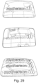
- FIGS. 19-31 are generally directed to examples of manufacturing decorative PVD coated items which contain gloss, satin and/or patterned metallic finishes with or without colored graphics with or without backlighting capability. These coated items may include other substrates which are not a radome such as any plastic substrate for use with vehicle parts.
- Example comprise rearview components like housings or scalps for exterior rearview mirror or exterior review camera systems.
- First side is to be understood as the side of the substrate, coating, or specific layer which in-use faces away from a radio wave transmitting or receiving device. As such, the first side is the side which is facing toward the external environment. In the specific context of a vehicle, this would be the visible outside of the vehicle.
- “Second side” is to be understood as the opposing side to the first side. In an in-use context this is the side facing toward the radio wave transmitting device, or receiving device. Typically, the second side is not visible when the radome is used.
- First surface is to be understood to refer to the surface on the first side of a substrate, coating, or specified layer.
- Siliconed surface is to be understood to refer to the surface on the second side of a substrate, coating, or specified layer.
- reflective refers to reflection of visible light, typically in the nanometre wave length and frequency range of 400 to 800 THz.
- a reference to radio wave throughout the specification typically refers to frequencies of 10MHz to 3000GHz.
- the frequency is typically 1000MHz to 100GHz.
- the frequency is 21 GHz to 81GHz, or about 24 GHz to about 79 GHz or about 77 GHz to about 79 GHz, or about 24 GHz, about 77 GHz or about 79 GHz.
- Use of about in this context does not exclude explicit limitation to specified band (e.g. 24 GHz) but does envisage the typical band spread used in the applications such as automotive radar systems. These band widths are known in the art for example see Hasch et al. "Millimeter-Wave Technology for Automotive Radar Sensors in the 77 GHz Frequency Band", IEEE Transactions on Microwave Theory and Techniques (Volume: 60, Issue: 3, March 2012 )
- transparent and “opaque” when used without a qualifier refers to visually transparent or opaque, and hence is a reference to transmission or absorption of visible light as defined above.
- the decorative radome of the present disclosure comprises a first surface or second surface coating, being a coating on the first side and in contact with the first surface of a substrate or on the second side and in contact with the second surface of a substrate.
- the first surface or second surface coating may include multiple "stacked" layers, with each layer having a first surface and a second surface, with the first surface of one layer abutting the second surface of an overlaying layer, which itself has a first surface.
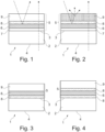
- a decorative radome (1) in accordance with the present disclosure is illustrated in Figures 1 to 6 and includes: a radio-transmissive substrate (2) having a first surface (3) on a first side and a second surface (4) on a second side; a radio-transmissive decorative coating (5) on the first surface (3) of the radio-transmissive substrate (2), the radio-transmissive decorative coating (5) including a decorative layer (6) consisting of a metal or consisting of an alloy including a metal.
- the radome of the present disclosure permits radio waves to traverse the radome (long dashes) while some visible light (short dashes) is reflected off the decorative layer (6), such that the appearance of the radome (1) is coloured or reflective.
- the radome (1) of the present disclosure is for use in the intended radio wave path of a transmitter and/or a receiver for a radio communication system or radio detection and ranging system, as such the design of the radome may be dictated by its intended use. Consequently, the selection of materials for the radio-transmissive substrate (2) will be, in part, dictated by design considerations, which are not solely based on the degree of radio-transparency such as robustness, moldability, resistance to extreme temperatures and cost. As such, the radio-transmissive substrate (2) can be any substrate, which attenuates the desired radio wave frequency at an acceptable level for the desired application. As is understood, all substrates will attenuate and reflect radio-waves to an extent.
- the substrate is a polymer, preferably a synthetic polymer.
- radio-transmissive substrates are typically resistant to electrical conductivity (i.e. are insulating or are a dielectric).
- Suitable polymers for the substrate (2) include (but are not limited to): Acrylonitrile Ethylene Styrene (AES), Acrylonitrile butadiene styrene (ABS), acrylonitrile styrene acrylate (ASA), Polyamide (PA), polybutylene terephthalate (PBT), Polycarbonate (PC), Polyethylene (PE), Polyethylene Teraphthalate (PET), Poly(methyl methacrylate) (PMMA), Polyoxymethylene (POM), Polypropylene (PP), Polyurethane (PU), PolyVinyl-Chloride (PVC), high-flow AES, acrylonitrile-(ethylene-propylene-diene)-styrene (AEPDS), blends of thermoplastics, or PC-ABS blended thermoplastic.
- the radio-transmissive substrate (2) will be formed of Polycarbonate or Polypropylene.
- the decorative layer (6) of the decorative coating (5) is preferably a reflective layer, and includes any suitable metal or alloy including a metal that provides the desired reflectivity, or appearance while being radio-transmissive.
- the metal which forms the decorative layer (6) is a transition metal.
- the metal which forms the decorative layer (6) is indium or tin.
- the decorative layer (6) is an alloy including a metal
- the alloy comprises a metal selected from the group of: aluminium, tin, indium or chromium.
- the decorative layer (6) includes a metalloid.
- Metalloids include silicon, boron, germanium, arsenic, antimony and/or tellurium.
- the metalloid is germanium or silicon.
- the metalloid is germanium.
- Suitable metalloid/metal alloys include germanium and aluminium and/or silicon; or germanium and silicon; or germanium and silver and, optionally, silicon; or germanium and indium and, optionally, silicon; or chromium and germanium and/or silicon.
- the alloy is not silicon and aluminium.
- the concentration of germanium may be at least 25wt% germanium, or at least 40wt% germanium, or at least 45wt% germanium, or at least 50wt% germanium, or at least 55wt% germanium.
- the decorative layer (6) consisting of a metal or consisting of an alloy including a metal.
- the decorative layer (6) is deposited by Physical Vapour Deposition (PVD). Suitable PVD methods include magnetron sputtering and evaporation, which may be resistive thermal evaporation or electron-beam evaporation.
- the decorative layer (6) is deposited by magnetron sputtering.
- the decorative coating (5) includes multiple layers, with the decorative layer (6) being abutted by one or more additional layer(s).
- the multiple layers of the decorative coating (5) includes a bonding layer.
- the bonding layer will directly abut the substrate and will therefore form the first layer in a multi-layer stack.
- a hard coat layer (7) may be provided to the first surface (3) of the substrate (2) prior to the addition of further layers in the decorative coating.
- Such a hard coat layer (7) acts to improve the bonding strength of the decorative layer (6) to the substrate (2) thereby reducing the likelihood of delamination of the coating (5) from the substrate (2).
- the hard coat (7) may also influence the overall residual stress of the radio-transmissive decorative layer (5) and as such may act, at least in part, as a stress controlling layer.
- the radio-transmissive decorative coating (5) includes a stress controlling layer which may underlie or overlie the radio-transmissive decorative layer (6). Therefore, as illustrated in Figures 1, 2, 4 , 5 and 6 a stress controlling layer (8) is on the first side (preferably the first surface) of the decorative layer (6).
- the radio-transmissive decorative coating may include a stress controlling layer (8) below the decorative layer (6).
- the stress controlling layer (8) is between the radio-transmissive substrate and the decorative layer (6).
- the stress controlling layer can be positioned above a hard coat (7) on the first surface (3) of the radio-transmissive substrate (2) and below the decorative layer (6).
- the multiple layers of the radio-transmissive decorative coating (5) include at least one dielectric layer, in the exemplified embodiments this dielectric layer is the stress controlling layer (8).
- the dielectric layer may also alter the visual characteristics of the decorative coating (5). This is particularly relevant in embodiments with multiple decorative layers (6) or an upper most dielectric layer (8) ( Figures 1, 2, 4 , 5 and 6 ).
- Suitable dielectrics for thin film deposition are known in the art and include oxides such as hafnium dioxide (HfO 2 ), aluminium oxide (Al 2 O 3 ), zirconium dioxide (ZrO 2 ), titanium dioxide (TiO 2 ) and silicon dioxide (SiO 2 ).
- the dielectric layer is silicon dioxide (SiO 2 ).
- the radio-transmissive decorative coating (5) includes at least one layer consisting of a metal or an alloy including a metal (6) between at least two dielectric layers (8) (see Figure 4 and 5 ). Additionally, in the embodiment illustrated in Figure 5 , the decorative coating (5) includes two decorative layers (6) sandwiched between alternating dielectric layers (8). These multilayer stacks allow for tuning of the radio-transmissive decorative coating (5), including its colour and residual stress.
- radio-transmissive decorative coating which includes multiple stacked layers.
- multi-layer stacks include:
- Such visual stacks could include a stress controlling layer to optimise the residual stress of the radio-transmissive decorative coating (5) within a desired window.
- this stress window is greater than or equal to -120MPa, or greater than or equal to -70Mpa, or greater than or equal to -50Mpa, or greater than or equal to -40MPa.
- Suitable materials for controlling stress include a dielectric layer, such as a further silicon dioxide layer, which can be tuned to provide a desired stress range (e.g. by altering thickness and deposition conditions) without altering the visual appearance of the decorative coating.
- a radome The inherent function of a radome is to provide protection to radar equipment from the environment. As such, the radome is susceptible to degradation, wear and damage. This exposure is further amplified when the radome is positioned at the front of a vehicle that is routinely exposed to relatively high speeds, abrasives, projectiles as well as chemicals used for cleaning.
- the outer most layer of the decorative coating (5) is a protective hard coat (9).
- a coating that is said to be a "hard coat” is a coating that is harder or more resilient (e.g. chemical resilient) than the underlying layers, whereby it increases the abrasion resistance, resistance to environmental damage or chemical resistance of radome.
- intermediate layers of the decorative coating (5) can also include a hard coat layer (7).
- This may be a hard coat of the same material, or of different material, to the protective hard coat (9).
- the hard coat(s) increase the abrasion resistance of the surface.
- Abrasion resistance can be measured through standard tests such as ASTM F735 "Standard Test Method for Abrasion Resistance of Transparent Plastics and Coatings Using the Oscillating Sand Method", ASTM D4060 “Standard Test Method for Abrasion Resistance of Organic Coatings", by the Taber Abrader, or by using the well-known Steelwool Test.
- a hard coat (7, 9) ideally provides at least the first surface of the radome with such chemical resistance.
- a hard coat (7, 9) is preferably formed from one or more abrasion resistant layers and may include a primer layer that bonds well to the underlying layer and forms a preferable surface for subsequent upper layers.
- the primer layer may be provided by any suitable material and may for example be an organic resin such as an acrylic polymer, a copolymer of an acrylic monomer and methacryloxysilane, or a copolymer of a methacrylic monomer and an acrylic monomer having a benzotriazole group or benzophenone group. These organic resins may be used alone or in combinations of two or more.
- the hard coat layer(s) (7, 9) is/are preferably formed from one or more materials selected from the group consisting of an organo-silicon, an acrylic, a urethane, a melamine or an amorphous SiO x C y H z .
- the hard coat layer(s) (7, 9) is/are an organo-silicon layer, due to its superior abrasion resistance and compatibility with physical vapour deposited films.
- a hard coat layer comprising an organo-silicon polymer can be formed of a compound selected from the following compounds: trialkoxysilanes or triacyloxysilanes such as, methyltrimethoxysilane, methyltriethoxysilane, methyltrimethoxyethoxysilane, methyltriacetoxysilane, methyltripropoxysilane, methyltributoxysilane, ethyltrimethoxysilane, ethyltriethoxysilane, vinyltrimethoxysilane, vinyltriethoxysilane, vinyltracetoxysilane, vinyltrimethoxyethoxysilane, phenyltrimethoxysilane, phenyltriethoxysilane, phenyltriacetoxys
- the hard coat layer(s) (7, 9) may be coated by dip coating in liquid followed by solvent evaporation, or by plasma enhanced chemical vapour deposition (PECVD) via a suitable monomer, flow coating or spray coating.
- PECVD plasma enhanced chemical vapour deposition
- subsequent coatings of the hard coat may be added, preferably within a 48-hour period so as to avoid aging and contamination of the earlier coatings.
- the thickness of the hard coat layer(s) (7, 9) is preferably selected to assist in providing adequate abrasion resistance, or to improve the bonding of the subsequent layers to the radio-transmissive substrate (2).
- the appropriate abrasion resistance will be determined by the required application and the demands of the user. In some applications, adequate abrasion resistance may be regarded as being a Bayer abrasion ratio of 5 with respect to an uncoated radio-transmissive substrate (2) (such as a polycarbonate), or alternatively by a Taber abrasion test with delta haze less than 15% after testing with a 500g load and CS10F wheel at 500 cycles, (% haze being measured as per ASTM D1003).
- the thickness of the hard coats is preferably at minimum of at least 1 ⁇ m thick on average and/or has a maximum thickness of 25 ⁇ m thick.
- the thickness of the hard coat layer (7) provided to the first surface (3) is from 1 ⁇ m to 15 ⁇ m.
- the thickness of the of the hard coat layer (7) provided to the first surface (3) is from 2 ⁇ m to 10 ⁇ m, or from 2 ⁇ m to 9 ⁇ m.
- the thickness of the protective hard coat layer (9) is from 5 ⁇ m to 25 ⁇ m.
- the thickness of the of the protective hard coat layer (9) is from 8 ⁇ m to 20 ⁇ m, or from 8 ⁇ m to 16 ⁇ m.
- the protective hard coat (9) can also modify the appearance of the decorative layer (6). As illustrated in Figure 2 , the protective hard coat (9) includes an additive to diffuse reflected visible light. Consequently, the decorative layer (6) has an outward "satin" appearance.
- This disclosure is however not restricted to provide a uniform satin appearance over the complete decorative coating.
- This disclosure allows to provide a visual feature wherein only a part, for example a logo, provides a satin graphic or pattern within the decorative coating, especially at least partly provided by a PVD coating method on a substrate, especially the substrate 2.
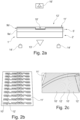
- a radome (1') comprising a substrate (2') and a decorative coating (5') providing such a satin pattern is shown.
- the decorative coating (5') comprises a different layer structure including a first hard coat (9a'), a second hard coat (9b') as well as a further coating layer (10').
- the hard coat (9b') might be replaced by a reflective coating. This reflective coating has a low optical transmission.
- the satin graphic is provided by first applying the hard coat layer (9a') to the, especially plastic and/or polycarbonate, substrate (2').
- the hard coat layer (9a') can be provided by dip coating with a polysiloxane hardcoat, for example PHC-587B of Momentive. After the dip coating the material is allowed to flash off and cure. In this way a hard coat layer (9a') for example having a thickness of more than 3 ⁇ m can be provided.
- the second hard coat layer (9b') is provided.
- the hard coat layer (9b') might be provided by a PVD coating process using a batch coating vacuum chamber.
- the hard coat layer (9b') is opaque for visual light.
- a hard coat layer with silica and a metal be provided to create a highly reflective surface.
- a reflective coating of low optical transmission is applied
- magnetron sputtering might be used to apply the reflective coating.
- the reflective coating might be a reflective PVD coating.
- a dielectric intermediate layer might be used between the reflective coating and the hard coat layer (9a').
- a recess (10') is generated to provide the wanted pattern / graphic.
- This recess (10') is generated by laser etching out of the second hard coat layer (9b') in selected areas.
- the recess (10') is generated by laser etching out of the reflective coating and, if used, the optional dielectric intermediate layer.
- the laser also etches the first hard coat layer (9a') below the second hard coat layer (9b'), reflective coating and/or dielectric intermediate layer in the area of the recess.
- a laser marking system operating at a 1064nm wavelength might be used for this etching process.
- a velocity of 500 - 1200 mm/s at a frequency 30 - 80 kHz of laser pulses might be used.
- optical coating (11') is generated covering the hard coat layer (9b') or the reflective coating used instead of the hard coat layer (9b') and the etched hard coat layer (9a'), especially in the area of the recess (10').
- This optical coating (11') might be applied after a cleaning of the surface and/or the optical coating (11') is generated by magnetron sputtering.
- the optical coating (11') can comprise several layers including metals, metalloids and dielectrics).
- the optical coating (11') By applying the optical coating (11') the previously invisible texture produced by the laser etching become now highly visible as diffuse light reflection is creating a satin appearance.
- An optional protective coating can be applied with or without a satin additive.
- a further advantage of the decorative coating shown in Figures 2a to 2c is that it allows a back lighting of the visual feature.
- illumination sources (14') might be located.
- the radome (1') is illuminated by the light sources (14'), for example comprising respective LED arrays for a viewer (16') the following visual effect is achieved.
- the hard coat layer (9a') is illuminated by the scattering effect of the surface in this area.
- the hard coat layer (11') in the areas (12') Due to the hard coat layer (11') in the areas (12') the light is however attenuated and these areas are not or less visible for a viewer (16') but remains reflective for light falling onto it from the side of the viewer (16').
- various aesthetic effects can realised for product styling purposes by backlighting.
- the hard coat layer (9b') is opaque or the reflective coating is used instead of the had coat layer (9b') any light bleed outside the area of the recess (10') is avoided and no double imaging will occur from reflection of light in this area at different surfaces, especially the surface of the hard coat layers (9a') and (9b') or the reflective coating used instead of the had coat layer (9b').
- the use of the before described decorative coating comprising the hard coat layers (9a') and (9b') an also be applied to the second alternative of the inventive radome.
- the layer (11') might be replaced by the overmolded layer and/or the second hard coat layer (9b') does not have to be highly reflective and/or opaque.
- a cap layer may also be provided by materials having characteristics, including: hydrophobic, hydrophilic, lipophobic, lipophilic and oleophobic or combinations thereof.
- a highly stressed interface between layers of the decorative coating (5), and between the decorative coating (5) and the substrate (2), should ideally be avoided to prevent a high region of stress becoming a locus for failure.
- a compressive layer pulls in one direction against a tensile layer pulling in the opposite direction, generating a high interfacial stress. It has been found that by controlling this interfacial stress (reducing it) the resilience of the decorative coating (5) can be improved.
- the present inventors have thus found that it is preferred to control internal stress parameters of the decorative coating (5) such that the differential stress is minimised.
- the present inventors have also found that it is further preferred to control internal stress parameters of a decorative coating (5) such that the net residual stress is above -120MPa.
- the net residual stress is above -70Mpa, or above -50Mpa, or above -40MPa.
- the net residual stress is neutral or is tensile (i.e. above 0MPa).
- decorative coatings (5) including a decorative layer (6) of aluminium and germanium the net residual stress will be above -120MPa, or above -50Mpa, or above -40MPa.
- the net residual stress will preferable be above -70Mpa, preferably up to +170Mpa.
- residual stress is to be taken as meaning the combined stress of the multiple layers which form the decorative coating (5), which may, or may not, include the protective hard coat (9). In preferred embodiments the residual stress is measured or calculated with the protective hard coat (9).
- the method of producing a decorative radome according to the second alternative is illustrated in Figure 12 and includes the steps of (102) preparing or providing a (radio-transmissive) substrate.
- the radio transmissive substrate will have a first surface (122) and a second surface (123 - see Figure 13 ).
- the method further includes (105) applying a decorative layer and/or coating (124) to a portion of the second surface (123) of the substrate (121), preferably a portion including the relieved portion (125), wherein the decorative layer and/or coating (124) comprising a metal or an alloy comprising a metal and a metalloid.
- the methods further includes (107) overmolding at least the decorative layer and/or coating (124) with a radio-transmissive polymer to provide an overmolded layer (126).
- the term "second surface” as used in the context of the following description relates to a surface upon which a decorative layer (124) may be applied and which may be overmolded.
- the term "first surface” is used in opposition to the second surface.
- the radio-transmissive substrate (121) is substantially transparent when formed and will provide the front most surface of the radome, when in use.
- the term “first surface” relates to the forward most surface of the substrate (121), when viewed.
- the first surface (122) will be the in the following description the front surface of the radio-transmissive substrate (121) of the badge when viewed from the front of the automobile.
- the measures described in the following paragraphs regarding the provision of the substrate, the intermediate layer, the hard coat, the shadow masking, the decorative layer and/or coating and/or the Surface Coating(s) and regarding the heating can also be at least partly used for the radome according the first alternative of this disclosure.
- the radio-transmissive substrate (121) can be provided by any desired method.
- the substrate (121) is injection moulded to form the desired shape.
- the substrate (121) may be received already formed.
- the substrate (121) includes a relieved portion (125) defining a three-dimensional visual feature on the second surface (123) of the substrate (121).
- the relieved portion (125) may be provided by a recess toward the first (122) surface of the substrate (121).
- the substrate (121) and overmolded layer (126) can be formed of any suitable material, but is preferably a plastic. As would be understood in the art, radio-transmissive substrates are typically resistant to electrical conductivity (i.e. are insulating or are a dielectric). Suitable polymers for the substrate (121) or overmolded layer (126) include Acrylonitrile Ethylene Styrene (AES), Acrylonitrile butadiene styrene (ABS), polycarbonate (PC), high-flow AES, acrylonitrile-(ethylene-propylene-diene)-styrene (AEPDS), blends of thermoplastics, or PC-ABS blended thermoplastic. In some embodiments, the substrate (121) will be formed of Polycarbonate.
- AES Acrylonitrile Ethylene Styrene
- ABS Acrylonitrile butadiene styrene
- PC polycarbonate
- AEPDS acrylonitrile-(ethylene-propylene-diene)-sty
- one of either the substrate (121), or the overmolded layer (126), is substantially transparent. This allows viewing of the decorative layer and/or coating (124) through the transparent layer.
- the other layer is substantially opaque to visible light.
- the opaque layer masks the equipment positioned behind the radome, and can modify, or improve, the visual aspects of the decorative layer and/or coating (124). For example improve the colour, or reflectivity, of the decorative layer and/or coating (124) by minimising light transfer through the decorative layer and/or coating (124).
- the transparent layer forms the outermost (forward) layer.
- the radio-transmissive substrate (121) is transparent and the overmolded layer (126) is opaque.
- the method includes the step of providing an intermediate layer (129) to at least a portion of the second surface of the radio transmissive substrate (121).
- the intermediate layer (129) is applied prior to the application of the decorative layer and/or coating (124) and can be applied prior to, or following on from, the deposition of a second surface coating (128) (in embodiments where one is applied).
- the intermediate layer (129) can be used to influence the appearance of the decorative radome produced by the method of the disclosure.
- the intermediate layer (129) can be a coloured layer which applies visual colour to the decorative radome.
- the intermediate layer (129) may also be a masking layer (which may be removable prior to overmolding or may be clear and remain in the decorative radome once produced) that assists in preventing application of the decorative layer and/or coating (124) to unwanted portions of the radio-transmissive substrate (121).
- the intermediate layer (129) is not substantially overlaid, or not overlaid, with the decorative layer and/or coating (124) when the radome is completed.
- the intermediate layer (129) could be an oil, liquid or ink mask, for example Fomblin TM , Krytox TM , SpeedMask TM .
- the intermediate layer (129) is applied by printing.
- the intermediate layer can withstand temperatures at or above 150°C, 175°C, 200°C, 220°C, 250°C, 275°C or 300°C for a minimum of 5, 10, 20, 30, 40 or 50 seconds, or 1, 1.5 or 2 minutes.
- the intermediate layer (129) may be any suitable layer, and in a preferred embodiment the intermediate layer (129) is an ink, dye, oil, wax, lubricant or other suitable liquid or coloured film. In some embodiments, the intermediate layer is an ink. The ink can be deposited by any suitable method. In some embodiments, the intermediate layer (129) is printed. Printing methods may include dye diffusion thermal transfer, wax thermal transfer, indirect dye diffusion thermal transfer, screen printing, inkjet printing or gravure printing process such as pad printing. In some embodiments, the intermediate layer (129) is applied by pad printing.
- thermo-stable ink such as Norilit TM U made by Procell, Inc. can be pad printed onto a three dimensional substrate, such as the radio transmissive substrate (121), and can tolerate temperatures up to 220°C for more than two minutes.
- Other suitable inks and printing methods are known in the art, and can be used with this disclosure.
- the method includes the further step of providing at least a portion of the second surface (123) of the radio-transmissive substrate (121) with a hard-coat (128).
- the application of a hard-coat to at least a portion of the second surface (123) of the radio-transmissive substrate (121) may provide advantageous functions, including (but not limited to): increasing or influencing the bonding between the decorative layer and/or coating (124) and/or intermediate layer (129) with the radio transmissive substrate (121); controlling the residual stress and/or thermal expansion of the decorative layer and/or coating (124); tuning the colour, reflectivity or other visual appearance of the decorative layer and/or coating (124) and/or intermediate layer (129); and/or providing an interface between portions of the radio-transmissive substrate (121) and the overmolded second layer (126) thereby influencing the adhesion bond between the two (without been an adhesive layer).
- Suitable hard-coat layers (128) are described below under heading 7 "Applying Surface Coating(s)".
- the method of the present disclosure may include the step of (104) providing a shadow mask.
- the shadow mask facilitates selective application of decorative layer and/or coating (124) on the radio-transmissive substrate (121).
- the type of shadow mask used will depend on the technique used to apply the decorative layer (124).
- the shadow mask is compatible with PVD, in particular sputtering and evaporation.
- the shadow mask is stainless steel.
- the shadow mask can be attached to each radio-transmissive substrate (121) prior to application of the decorative layer and/or coating (124) or can be positioned within the deposition machine, such as on the target side of a PVD machine.
- the decorative layer and/or coating (124) is applied only to a portion of the second surface (123) of the substrate (121) to provide a visual feature on the radio-transmissive substrate (121).
- the decorative layer and/or coating (124) is applied to the relieved portion (125).
- the decorative layer and/or coating (124) By applying the decorative layer and/or coating (124) to only a portion of the substrate (121), this allows direct adhesion bonding between the first (radio-transmissive substrate) layer (121) and the (second) overmolded layer (126) in portions not provided with the decorative layer and/or coating (124). In the absence of this direct adhesion binding between the substrate (121) and the overmolded layer (126), the layers may separate.
- the decorative layer and/or coating (124) is preferably a reflective layer, and includes any suitable metal, metalloid or metal/metalloid alloy that provides the desired reflectivity, or decorative appearance while being radio-transmissive.
- the metal, which forms the decorative layer and/or coating (124) includes transition metals.
- the metal which forms the decorative layer and/or coating (124) is Indium or Tin.
- a reflective layer is abutted by additional layers.
- the reflective layer is between two layers of deposited Silicon. These multilayer stacks allow for tuning of the layer, including its colour and residual stress.
- multiple layers including a layer of Silicon followed by a layer of Aluminium/Silicon and then a further layer of Silicon, are deposited to the substrate (121) to form the decorative layer and/or coating (124) prior to overmolding.
- the decorative layer and/or coating (124) includes a metalloid.
- Metalloids include Silicon, Boron, Germanium, Arsenic, Antimony and/or Tellurium.
- the metalloid is Silicon or Germanium.
- the metalloid is Germanium.
- Suitable metalloid/metal alloys include: Germanium and Aluminium and, optionally, Silicon; or Germanium and Silicon; or Germanium and Silver and, optionally, Silicon; or Germanium and Indium and, optionally, Silicon; or Aluminium and Silicon.
- the alloy of Germanium is Germanium and Aluminium, or Germanium and Silicon, or Germanium and Aluminium and Silicon.
- the alloy is Silicon and Aluminium.
- the metalloid/metal alloy includes Germanium
- the alloy is at least 25wt% germanium, or at least 40wt% germanium, or at least 45wt% germanium, or at least 50wt% germanium, or at least 55wt% germanium.
- the decorative layer and/or coating (124) is provided as a thin-coating layer.
- the average thickness of the decorative layer (124) is 20 - 190nm thick, or 40 to 170nm thick, or 60 to 150nm thick.
- Such thin-coatings can be provided by multiple methods in the art.
- the decorative layer (124) is deposited by Physical Vapour Deposition (PVD). Suitable PVD methods include magnetron sputtering and evaporation, which may be resistive thermal evaporation or electron-beam evaporation.
- the decorative layer (124) is deposited by magnetron sputtering.
- the moulding of the radio-transmissive substrate (121) (in embodiments whereby the radio-transmissive substrate is moulded), the application of any intermediate layers (129), and the application of the decorative layer and/or coating (124) are performed in the same machine.
- each step can be performed by separate machines arranged to operate sequentially.
- the substrate (121) and the decorative layer and/or coating (124) Prior to providing a second-shot overmolded layer (126), it may be advantageous to heat the substrate (121) and the decorative layer and/or coating (124). Such heating (106) permits a degree of thermal expansion at a rate slower than that which will be encountered during the overmolding process (107) and as such will limit the rate of change in temperature of the decorative layer (124), and the substrate (121), during overmolding. This reduces visual defects, such as crazing, during the overmolding step (107). Therefore, in some embodiments of the method of this disclosure, the substrate (121) and the decorative layer and/or coating (124) are heated prior to overmolding. In some embodiments, the substrate (121) and the decorative layer (124) are heated to at least 70°C, or to at least 80°C prior to the overmolding step (107).
- the overmolded layer (126), once set, provides a third (rear) surface (127) which is parallel or substantially parallel, to the first surface (122) of the radio-transmissive substrate (121), over at least a portion of the radome.
- the parallel or substantially parallel portion defining a radio path through which radio waves can traverse.
- the parallel or substantially parallel nature of the first and third surface minimise difference in the refraction of the radio waves as they traverse different potions of the radio path of the radome.
- thermoplastics/thermo-polymers have different flow temperatures and therefore require different barrel nozzles for injection moulding. Typically, higher temperatures will increase the likelihood of damage and visible defects in the decorative layer and/or coating (124) when overmolded. Therefore, it is preferable to use thermoplastics/thermo-polymers with a relatively low nozzle temperature, or a nozzle temperature below the crazing point of the decorative layer and/or coating (124).
- the melt temperature and mould temperature for a range of common thermoplastics is provided in Table 1 below.
- Table 1 - Thermoplatics melt temperatures and desired mould temperatures.
- MELT TEMPERATURE RANGE (°C) MOULD TEMPERATURE RANGE (°C) ABS 190-270 40-80 ABS/PC ALLOY 245-265 40-80 ACETAL 180-210 50-120 AES 215-260 55-65 PMMA 220-250 50-80 CAB 170-240 40-50 HDPE 210-270 20-60 LDPE 180-240 20-60 NYLON 6 230-290 40-90 NYLON 6 (260% GF) 250-290 50-90 NYLON 6/6 270-300 40-90 NYLON 6/6 (263% GF) 280-300 40-90 NYLON 11 220-250 40-110 NYLON 12 190-200 40-110 PEEK 350-390 120-160 POLYCARBONATE 280-320 85-120 POLYESTER PBT 240-275 60-90 PET (
- thermoplastic materials are provided by the International Organisation for Standardization, and are particularly set forth in the Standards Catalogue 83.080.20.
- the overmolded layer (126) is formed with a barrel nozzle temperature at or below 300°C.
- the barrel nozzle is at or below 280°C during the overmolding process (107).
- the barrel nozzle is at or below 250°C during the overmolding process (107).
- the barrel nozzle is at or below 230°C during the overmolding process (107).
- Suitable polymers, which are capable of being injection moulded at these barrel nozzle temperatures are known in the art and are determined by their melt temperature.
- some embodiments of the method of the disclosure include providing the first surface (122) of the radio-transmissive substrate (121) with a hard-coat (128).
- the inherent function of a radome is to provide protection to radar equipment from the environment. As such, the radome is susceptible to degradation, wear and damage. This exposure is further amplified when the radome is positioned at the front of a vehicle that is routinely exposed to relatively high speeds, abrasives, projectiles as well as chemicals used for cleaning.
- a coating (128) that is said to be a "hard-coating” is a coating that is harder than the radio-transmissive substrate (121), whereby it increases the abrasion resistance of that radio-transmissive substrate (121).
- Such an abrasion resistant hard-coating (128) is one that reduces damage due to impacts and scratching.
- Abrasion resistance can be measured through standard tests such as ASTM F735 "Standard Test Method for Abrasion Resistance of Transparent Plastics and Coatings Using the Oscillating Sand Method", ASTM D4060 "Standard Test Method for Abrasion Resistance of Organic Coatings", by the Taber Abrader, or by using the well-known Steelwool Test.
- plastics can be damaged by certain solvents; for example, polycarbonate is damaged by acetone.
- polycarbonate is damaged by acetone.
- radomes it is a requirement for many exterior automotive components, such as radomes, that they be "chemically resistant", which is a reference to an ability to withstand exposure to normal solvents such as diesel fuel, petroleum, battery acid, brake fluid, antifreeze, acetone, alcohol, automatic transmission fluid, hydraulic oil and ammonia based window cleaners.
- a hard-coating ideally provides at least the first surface of the radome with such chemical resistance.
- a hard-coating (128) on the first (122) and/or second (123) surface of the radio-transmissive substrate is preferably formed from one or more abrasion resistant layers, and may include a primer layer that bonds well to the substrate (121) and forms a preferable surface for subsequent abrasion resistant layers.
- the primer layer may be provided by any suitable material and may for example be an organic resin such as an acrylic polymer, a copolymer of acrylic monomer and methacryloxysilane, or a copolymer of a methacrylic monomer and an acrylic monomer having a benzotriazole group or benzophenone group. These organic resins may be used alone or in combinations of two or more.
- the hard-coat layer(s) (128) are preferably formed from one or more materials selected from the group consisting of an organo-silicon, an acrylic, a urethane, a melamine or an amorphous SiO x C y H z .
- Momentive PHC-587B momentive UVHC 5000 (which is UV cured) and the two part product comprising a primer of PR6600 (SDC Technologies), subsequently coated with MP101 (SDC Technologies).
- the hard-coat layer(s) (128) is/are an organo-silicon layer, due to its superior abrasion resistance and compatibility with physical vapour deposited films.
- a hard-coating layer comprising an organo-silicon polymer can be formed of a compound selected from the following compounds: trialkoxysilanes or triacyloxysilanes such as, methyltrimethoxysilane, methyltriethoxysilane, methyltrimethoxyethoxysilane, methyltriacetoxysilane, methyltripropoxysilane, methyltributoxysilane, ethyltrimethoxysilane, ethyltriethoxysilane, vinyltrimethoxysilane, vinyltriethoxysilane, vinyltracetoxysilane, vinyltrimethoxyethoxysilane, phenyltrimethoxysilane, phenyltriethoxysilane, phenyltriacetoxy
- the hard-coat layer(s) (128) may be coated onto a substrate (such as the radio-transmissive substrate (121)) by dip coating in liquid followed by solvent evaporation, or by plasma enhanced chemical vapour deposition (PECVD) via a suitable monomer, flow coating or spray coating.
- a substrate such as the radio-transmissive substrate (121)
- PECVD plasma enhanced chemical vapour deposition
- subsequent coatings of the hard-coating may be added, preferably within a 48 hour period to as to avoid aging and contamination of the earlier coatings. These additional coatings may be added to either the first (122) or second (123) surface of the substrate (121)
- the thickness of the hard-coat layer (128) is preferably selected to assist in providing adequate abrasion resistance.
- the appropriate abrasion resistance will be determined by the required application and the demands of the user. In some applications, adequate abrasion resistance may be regarded as being a Bayer abrasion ratio of 5 with respect to an uncoated plastic substrate (121 - such as a polycarbonate), or alternatively by a Taber abrasion test with delta haze less than 15% after testing with a 500g load and CS10F wheel at 500 cycles, (% haze being measured as per ASTM D1003). With these requirements met, when an organo-silicon is used as a hard-coat layer (128), the thickness of the hard-coating (128) is preferably at minimum of at least 6 ⁇ m thick on average and/or has a maximum thickness of 28 ⁇ m thick.
- a cap layer may also be provided by materials having characteristics, including: hydrophobic, hydrophilic, lipophobic, lipophilic and oleophobic or combinations thereof.
- the disclosure thus provides in the second alternative a decorative radome comprising; a first layer (121) comprising a radio-transmissive polymer, the first layer (121) having a front surface (122); a second layer (126) comprising a radio-transmissive polymer, the second layer (126) having a rear surface (127); and a decorative layer and/or coating (124) between the first (121) and second (126) layer comprising a metal or an alloy comprising a metal and a metalloid, wherein the second layer (126) directly abuts the decorative layer (124) and the first layer (121) is directly adhesion bound to the second layer (126), and wherein at least one of the first (121) or second (126) layers is comprised of a polymer (thermo-polymer) capable of being overmolded at a barrel nozzle temperature below 300 degrees Celsius.
- a polymer thermo-polymer
- the decorative radome of the disclosure can include a hard-coat (128) provided to the first surface (122) of the radome.
- the radome more precisely the substrate (221) comprises in the area of the decorative coating (224) a first surface structure formed by elements (230, 232).
- the elements (230) are formed as fungiform protrusions.
- the coating (224) encloses the protrusions (230) to reach a form fit connection.
- the elements (232) are formed as undercuts.
- parts of the decorative coating (224) reach into the undercuts (232) so that the decorative coating (224) is also form fit connected to the substrate (221).
- the substrate (221) furthermore comprises a second surface structure comprising elements (234, 236).
- the elements (234) are formed as groove-shaped undercuts.
- the overmold material also flows into the undercuts (234) thus providing a form fit connection between the substrate (221) and the overmold layer (226).
- fungiform projections (236) are formed in the substrate (221).
- the overmold material encloses the projections (236) to provide a from fit connection between the substrate (221) and the overmold layer (226).
- the surface structure might be provided by at least one separately formed anchor element.
- the surface structure does not have to necessarily be formed in one piece with the substrate and/or the decorative coating.
- the surface structure, especially the anchor element might be formed rom a material different to the material of the substrate and/or the decorative coating.
- the anchor element might be for example located in a mould before the substrate and/or the decorative coating is formed. In this way the anchor element is at least partly embedded and/or overmolded.
- the decorative radome of this disclosure does not substantially attenuate electromagnetic frequencies of 10MHz to 3000GHz.
- the radome has a radar attenuation less than 2dB one-way (4dB two-way) across a signal path, or preferably 1 dB one-way (2dB two-way) across a signal path.
- the decorative layer (124) comprising a metal or an alloy of metal and a metalloid, has a sheet resistivity greater than 10 6 ohms per square ( ⁇ / ⁇ ).
- the direct adhesion bond formed between the first layer (121) and the second layer (126) improves the weather resistance of the radome compared to radomes formed of layers bound by adhesives. Therefore, in some embodiments there is no water ingress between the first layer (121) and the second layer (24) when immersed in water at 60°C for 240hrs.
- the decorative radome according to the second alternative can be produced in accordance with the method disclosed above.
- the decorative radome can be produced by any suitable method that provides all of the required claimed features and functions.
- the decorative radome of this disclosure should be considered to optionally include, the structural and functional features disclosed above in relation to the method.
- the decorative radome of the present disclosure can be used in any suitable context.
- the radome is a car badge.
- the car badge may include additional features, functions and aesthetics.
- the radome can be used in combination with a light assembly, or may include additional features, as that described in WO2017/009260 and US patent application publication number 2018/0202626 A1 , each entitled "A LIGHT ASSEMBLY AND A VEHICLE DESIGN ELEMENT INCLUDING SUCH A LIGHT ASSEMBLY", and each of which is hereby incorporated by reference in its entirety for all purposes.
- reflective refers to reflection of visible light, typically in the nanometre wave length and frequency range of 400 to 800 THz. The percentage of reflectance can be measured using known techniques in the field, or as discussed below.
- a reference to radio wave throughout the specification typically refers to frequencies of 10MHz to 3000GHz.
- the frequency is typically 1000MHz to 100GHz.
- the frequency is 24 GHz to 79GHz, or 77GHz to 79GHz, 24GHz, 77GHz or 79GHz.
- transparent and “opaque” when used without a qualifier refers to visually transparent or opaque, and hence is a reference to transmission or absorption of visible light as defined above.
- the front and rear face should be parallel or substantially parallel. Further, the interior of the radome should have no voids, air bubbles or significant changes in material density such as water ingress, and the decorative layer should be of a uniform thickness.
- the surface resistivity of the decorative layer can be determined using a four-point method, using a four-point probes in accordance with JIS K7194. Surface resistivity should be above 10 6 ⁇ / ⁇ (Ohms per square) indicating low electrical conductivity (i.e. the reflective layer is electrically insulated in situ).
- Radio wave attenuation and reflectance will be determined by the requirements of the user, the application, the frequency used and the equipment being used. However, preferably there will be a minimum of 10dB reflection and a maximum of 1dB one-way (2dB two-way) transmission loss at the sensor operating frequency, typically 24GHz, 77GHz or 79GHz.
- the decorative radome of this disclosure does not substantially attenuate electromagnetic frequencies of 10MHz to 3000GHz.
- the radome has a radar attenuation less than 2dB one-way (4dB two-way) across a signal path, or preferably 1 dB one-way (2dB two-way) across a signal path.
- the decorative layer (6) comprising a metal or an alloy of metal and a metalloid, has a sheet resistivity greater than 10 6 ohms per square ( ⁇ / ⁇ ) in situ.
- the surface resistivity of the decorative layer (6) can be determined using a four-point method, using a four-point probes in accordance with JIS K7194.
- the front and rear face should be parallel or substantially parallel.
- the interior of the radome (1) should have no voids, air bubbles or significant changes in material density such as water ingress, and the decorative layer and/or coating (5, 124) should be of a uniform thickness.
- Radio wave attenuation and reflectance will be determined by the requirements of the user, the application, the frequency used, and the equipment being used. However, in some embodiments there will be a maximum of 2dB one-way (4dB two-way) attenuation at a specific operating frequency between 76 and 81 GHz. In some embodiments, there will be less than 2dB one-way attenuation at 24GHz, 77GHz or 79GHz. In some embodiments, there will be a maximum of 1dB one-way (4dB two-way) attenuation at a specific operating frequency between 76 and 81 GHz. In some embodiments, there will be less than 1dB one-way attenuation at 24GHz, 77GHz or 79GHz.
- the present disclosure provides a radar system as illustrated in Figure 7 including a radio wave transmitter (10), a radio wave receiver (10) and a decorative radome (1) as describe herein.
- the radome (1) can sit in the radio wave path of both the radio wave receiver and transmitter (which may be integrated into one device) or there may be a radome associated with the transmitter and another radome associated with the receiver.
- the substrate attenuates the radio wave signal as it traverses the radome (1).
- a portion of this attenuation is a product of the reflection of the radio wave signal from the first surface (3) or second surface of the substrate (2, 121) as the radio waves emanating from the transmitter traverse the radome. Consequently, the attenuation, as a result of reflection, is determined by the thickness of the substrate (2, 121) (and coating) as well as the possible overmold layer in relation to the wave length of the radio wave signal.
- the wave length of the radio wave through the substrate varies with the dielectric real permittivity of the substrate and/or the overmold layer.
- the substrate thickness providing minimum attenuation is determined by the equation m ⁇ i 2 , where m is an integer and ⁇ i is the wavelength through the substrate and/or overmolded layer of the radio wave transmitted from a radio wave transmitter for which the radome is designed. Consequently, in some embodiments the thickness of the radome substrate and/or overmold layer is a multiple of ⁇ i 2 .
- Radar systems in vehicles typically use microwaves to provide line-of-sight detection of objects.
- the three frequencies currently being used for automobiles are 24 GHz, 77 GHz and 79 GHz.
- 77 GHz and 79 GHz have become the dominant frequency used as these frequencies offer improved range and resolution compared to the 24 GHz frequency.
- 77 GHz can differentiate objects at a 3 times higher resolution than 24 GHz while using an antenna size three times less in height and width (with only ninth of the area).
- Radar systems using the 24GHz could utilise both a narrow band (NB) spanning 200MHz from 24.05 GHz to 24.25GHz and an ultra-wide band (UWB) spanning 5GHz, from 21.65GHz to 26.65GHz.
- NB narrow band
- UWB ultra-wide band
- the 24 GHz NB and UWB have been replaced with frequencies from 71 to 81GHz, with the 76 to 77 GHz range representing long range radar (LRR) and the 77 to 81 GHz representing short range radar (SRR).
- LRR long range radar
- SRR short range radar
- the 77 to 81 GHz range provides up to 4GHz of sweep bandwidth, which is much larger than the 200MHz available in the 24GHz NB.
- the radome is designed for use in, or is used in, a radar system wherein the radio wave transmitter (10) transmits radio waves in the frequency between 20 GHz and 81GHz. In some embodiments, the radome is designed for use in, or is used in, a radar system wherein the radio wave transmitter transmits radio waves in the frequency between 76 and 81 GHz, or from 76 to 77GHz, or is about 77GHz, or is about 79 GHz.
- the substrate is between 2mm and 2.6mm thick. In some embodiments, the substrate is about 1.15mm, 2.3mm or 2.45mm thick.
- the decorative radome (1) according to the first alternative of the present disclosure includes a layer including a heating element (11).
- a heating layer may also be provided in the radome according to the second alternative of the present disclosure.
- the heating layer might be an additional layer, especially an additional and/or alternative intermediate layer might be at least partly be formed by the overmold layer or might at least partly be formed by the substrate.
- Suitable heating elements compatible for use with radomes are disclosed in DE102014002438A1 , DE10156699A1 , US20180269569A1 which are hereby incorporated by way of this reference in their entirety and for all purposes.
- the heating element (11) comprises a radar-transparent polymer with an embedded resistance wire circuit (12), which may be embedded or molded within the heating element substrate (11) to form a network, which substantially covers the radome.
- the heating element (11) can be provided by a polymer film, containing the circuit (12) which can be provided between the radio-transmissive substrate (2) and the decorative coating (5).
- the heating element might also be formed at least partly by the overmold layer.
- the polymer film (11) will also need to be radio-transmissive. Consequently, the polymer film (11) can be made of any suitable polymer disclosed herein for the radio-transmissive substrate (2).
- the polymer film (11) may be made of a polymer selected from the group including (but are not limited to): Acrylonitrile Ethylene Styrene (AES), Acrylonitrile butadiene styrene (ABS), acrylonitrile styrene acrylate (ASA), Polyamide (PA), polybutylene terephthalate (PBT), Polycarbonate (PC), Polyethylene (PE), Polyethylene Teraphthalate (PET), Poly(methyl methacrylate) (PMMA), Polyoxymethylene (POM), Polypropylene (PP), Polyurethane (PU), PolyVinyl-Chloride (PVC), high-flow AES, acrylonitrile-(ethylene-propylene-diene)-styrene (AEPDS), blends of thermoplastics, or PC-ABS blended thermoplastic.
- the polymer film (11) containing the circuit (12) will be formed of Polycarbonate or Polypropylene.
- the circuit can be embedded in, or moulded into, the radio-transmissive substrate (2) of the radome (1), such that the circuit (12) is provided within the radio-transmissive substrate (2) without the requirement for an additional layer.
- Car emblems are traditionally employed to convey styling and branding on vehicles.
- the radomes according to the disclosure allow to incorporate such car emblems, for example a logo as visual feature.
- a logo as visual feature.
- a radome has preferably a uniform cross section of optimal thickness tuned according to the dielectric properties of the materials. It is also desirable to have minimal interfaces between dissimilar materials to not negatively influence the radio-transmissibility.
- the illumination of the badge usually make the use of additional parts for transmitting, diffusing, reflecting and piping light necessary, leading without further measures like increasing the entire thickness of the radome to a decrease of the radio-transmissibility due to the before described effects.
- the implementation of an illumination is often contrary to the interest of an optimal radio/radar performance.
- the inventive radomes allow however to provide an illumination avoiding the before described problems.
- This object is achieved by using the existing structure and elements at least partly as illumination system.
- a respective layer or coating is used as a light guide into which light of a light source is coupled in. the light is guided by the layer or coating and falls onto the visual feature from where it is reflected and/or scattered.
- Fig. 16 an exploded cross-sectional view of a radome, including an illumination system is shown.
- the elements of the radome corresponding to the radome as shown in Figure 13 have the same reference numbers however increased by 200.
- the radome of Figure 16 comprises a moulded substrate (321), preferably comprising polycarbonate that is transmissive for visual light.
- the substrate (321) is especially provided in a first shot moulding step.
- the coating (324) is especially radar/radio transparent and reflective for visual light and might comprise AIGe provided by a PVD coating process.
- the substrate (321) and the decorative coating (324) are overmolded by overmolded layer (326), being especially opaque for visual light but radio-/radar-transmissive.
- the overmolded layer (326) is especially provided in a second shot moulding step and/or comprises AES material, especially dark coloured AES.
- the decorative coating is encapsulated between the for visual light transparent substrate (321) and the for visual light opaque overmolded layer (326).
- the substrate (321) is furthermore protected by a second surface coating in form of a hard coat (328), especially thermal hard coat, as already explained in the embodiments before.
- FIG 16 furthermore a radio transceiver, especially comprising a radar unit (340) is shown.
- a radio transceiver especially comprising a radar unit (340) is shown.
- a viewer looking onto the radome is visualised for illustrative purposes by an eye (342).
- the illumination system of the radome comprises two light sources (344), especially comprising LEDs.
- the light sources (344) light rays (346) are coupled into the substrate (321).
- the substrate (321) forms partly also a part of the illumination system as acting as light guide for the light coupled into it from the light sources (344). The light is guided through the substrate (321) as indicated by arrows (348).
- the light is at least partly reflected / scattered by the decorative coating (324) into the direction of the viewer (324) as indicated by the arrows (350).
- the viewer can clearly see the visual feature, especially logo, formed by the decorative coating (324) by the illumination.
- the radome appear to be reflective for light whereas a view onto the radome along arrow (354) let the radome appear as black gloss due to the missing decorative coating in this area as well as the opaque, especially dark coloured overmold layer (326).
- the light sources (344) especially represent edge lighting sources as the light is coupled into the light guide in form of the substrate (321) in a direction being mainly perpendicular to the normal direction N of the surface of the substrate (321).
- the relieved portion (325) in the substrate (321) can be designed at an angle to optimize the pick up of the light guided through the substrate (321).
- the use of edge lighting sources has the advantage that the light sources (344) can be located outside a radars signal transmission/ receiving zone, and thus will not affect the radar sensing requirements.
- the light sources can be hidden behind a supporting structure of the radome, like a bezel, grill or the like.
- FIG 17 a further example of an inventive radome comprising an illumination system is shown.
- the elements of the radome shown in Figure 17 that correspond to the elements of the radome shown in Figure 16 have the same reference numbers however increased by 100.
- the use of the illumination system is not restricted to plane or flat radomes.
- the radome might also have a curved cross-section without negatively influencing the illumination function.
- the light of the light sources (444), shown as light rays (446) is coupled into the substrate (421).
- the substrate (421) acts as a light guide as the light rays within the substrate are undergoing internal reflection as shown by arrows (448).
- the light is not significantly scattered out of the substrate (421) but is guided along the substrate (421) until it falls onto the decorative coating (424) in the relieved area (425). From there it is reflected and/or scattered out of the substrate (421) along the arrows (450) to be seen by a viewer.
- FIG 18 a picture onto an actual radome including an illumination system as described before is shown.
- the elements of the radome shown in Figure 18 that correspond to the elements of the radome shown in Figure 17 have the same reference numbers however increased by 100.
- a view onto the second surface of the substrate (521) of the radome is shown.
- Light from light sources (544) is coupled into the substrate (521) and is reflected / scattered by the decorative coating (524) so that a visual feature in form of a logo (552) becomes visible.
- the illumination is reduced as only the opaque overmold layer (526) is visible.
- the illumination system has been described in combination with the second alternative of the disclosure the person skilled in the art recognized that the illumination system is also applicable to the first alternative.
- a layer neighbouring the decorative coating or a layer of the decorative coating neighbouring a reflective layer of the coating is used as a light guide.
- the stress controlling layer (8) or the hard coat layer (9) may allow the guiding of light to the reflective area of the decorative coating from where it is reflected and/or scattered.
- Polycarbonate has a relative permittivity ( ⁇ r) of 2.8 at 77 GHz, and therefore the calculated wavelength through the substrate is 2.328mm.
- the attenuation followed an inclined sine curve with attenuation cyclically being at a minimum with substrate thickness that were an integer multiple of half wave length (i.e. 0.5, 1, 1.5, 2, 2.5 etc. times the wavelength of the radio wave through the substrate), with maximum attenuation being a quarter wave length offset from the minimum (i.e. 0.75, 1.25, 1.75 etc. times the wavelength of the radio wave through the substrate).
- the average attenuation across the sine curve increased as the thickness of the sheet increased.
- the optimal thickness was selected at 2.3 mm, which provided minimal attenuation and appropriate robustness, stiffness and weight for use as an automotive body part.
- the mean attenuation across the 76-77GHz frequency was approximately 117% of the mean attenuation across the 76-81GHz frequency when the polycarbonate substrate was 2mm.
- the mean attenuation across the 76-77GHz frequency was approximately 83% of the mean attenuation across the 76-81 GHz frequency when the polycarbonate substrate was 2.3mm.
- the percent variation between the 2mm and 2.3mm substrates was 17% when the mean attenuation across the 76-77GHz frequency was compared to the mean attenuation across the 76-81GHz frequency, albeit in opposing directions.
- a radio-transmissive decorative polymer sheet was prepared with a gloss metallic look as per the following protocol.
- a polycarbonate substrate was prepared by applying a base hard coat layer of Momentive PHC587B using an automated dipcoating process consisting of a detergent wash, coarse rinse, fine rinse, extra fine rinse, drying, cooling and then dip coating and flash off.
- the dipcoating process was robotically controlled with a precise removal speed to control the thickness of the hardcoat.
- the first-surface hard coated substrate was left for 10 minutes to allow evaporation of the solvents until the surface was substantially tack-free. Subsequently, the first-surface coated substrate was cured for 71 minutes at 130°C in a curing oven to provide a hard coated substrate.
- a decorative coating including a layer of Aluminium and Germanium alloy and an overlying layer of silicon dioxide (SiO 2 ) was deposited in accordance with the following parameters: Table 2 - Decorative layer Coating Parameters Pre-Treatment Layer 1 Layer 2 Glow discharge electrodes (S/S) Power 3kW n/a n/a Dual rotatable Silicon Target (99.90% purity) n/a n/a Power 18kW Aluminium/Germanium (50/50wt%) n/a Power 30kW n/a Total Gas flow 740sccm Ar 100sccm O2 330sccm Ar 100sccm Ar 200sccm O2 RPM 6 24 24 Number of rounds 12 10 20 Base Pressure (mbar) 8e-5 1.5e-5 1.5e-5 Run Pressure (mbar) 9e-3 2e-3 7e-4 Thickness (nm) n/a 30 25
- a protective surface hard coat layer of Momentive PHC587B was applied as the upper (protective hard coat) layer of the decorative coating. This was completed by an automated spray coating process in a dedicated thin film coating spray booth. The first-surface coated substrate was left for 10 minutes to allow evaporation of the solvents until the surface was substantially tack-free. Subsequently, the first-surface coated substrate was cured for 71 minutes at 130°C in a curing oven to provide a protective hard coated surface.
- a radio-transmissive decorative polymer sheet was prepared with a satin metallic look as per the following protocol.
- a polycarbonate substrate was provided with a first surface hard coating and a decorative coating comprising a layer of an alloy of aluminium and germanium and silicon dioxide layer as set out for the "Gloss Metallic Look" set out above.
- a protective hard coat was applied which included an additive that resulted in diffusion of visible light. Specifically, the following parameters were used: Table 3 - Satin Hard Coat Deposition Parameters Layer 1 Material Momentive PHC-587B + Tospearl 2000B at a 3.5% wt/wt Deposition Method Spray Coated and cured at 130 °C Thickness ( ⁇ m) 8 to 16
- Gloss Metallic coating or a Satin Metallic coating as described above.
- the thickness of the applied decorative coating can be up to 0.03mm thick providing a total thickness of 2.03. 2.33, 2.95, 4.45 and 5.87mm.
- Table 5 Substrate Attenuation (dB); Reflection (%) Substrate Thickness (mm) Gloss Metallic Satin Metallic Attenuation dB (average) Reflection % (average) Attenuation dB (average) Reflection % (average) 2.03 1.31 34 1.33 34 2.33 1.13 10 1.18 9 2.95 1.69 35 1.63 37 4.45 1.43 31 1.36 32 5.87 1.24 19 1.31 21
- the one-way attenuation and reflection of coated 2.33mm polycarbonate did not significantly vary based on the coating applied. Further the best performing thickness was 2.33mm with an attenuation of 1.1dB and 1.18dB (Gloss, Satin) and a reflection of 10% and 9% (Gloss, Satin).
- Two-millimetre and 2.3mm polycarbonate substrates were coated to provide a Gloss Metallic Look or a Satin Metallic Look as described above and the visual characteristics at the centre of the coated substrates were measured via an illuminant A/2.
- the reflectivity including specular and diffuse reflected light (Rsin), was comparable for both gloss and satin metallic look samples.
- the reflectivity on the 2.3mm samples was typically higher than the 2mm samples. This was likely an artefact of the coating process as the 2.3mm samples consisted of small plaques, compared to the A4 sized 2mm samples, and as such the 2.3mm samples were closer to the splutter target during deposition.
- This coated item (which may not be a radome) may include gloss, satin and/or patterned metallic finishes with or without coloured graphics with or without backlighting capability.
- the coated item may include an rearview component like an exterior mirror scalp or exterior review camera scalp.
- FIGS. 19-22 illustrate an example of manufacturing a PVD coated item according to a first embodiment.
- a first step includes applying a hard coating (602) to a plastic substrate (603).
- a hard coating 602
- black polycarbonate may be dip coated in SilFort PHC587B and cured.
- a decorative PVD coating 601
- An optional dielectric intermediate layer may be used between the reflective coating and the hardcoated substrate.
- a pattern/graphic may be laser etched (604) into the decorative PVD coating (601).
- the PVD coating (601) may be either partially or fully removed. As a result of this process, areas are selectively ablated to provide a graphic using the contrast between the underlying substrate and the decorative PVD coating (601). Where the PVD is fully removed, a hardcoated surface remains, maintaining the integrity and robustness of the substrate.
- a graphic is produced by the absence of PVD material rather than the addition of another material.
- the graphic is produced as a result of contrast between the underlying substrate and decorative PVD coating.
- the parameters (power, velocity and Q-switch frequency) of the laser etch determine if the material is partially or fully removed.
- the durability of this solution is superior as the contrast is achieved by exposing the substrate.
- this technique cannot be easily affected by abrasion or chemicals such as when using painting or printing. Different colored graphics can be achieved with different substrate colors. And if the substrate is transparent to light, this solution offers backlighting ability.
- protective coating (600) can be applied with or without a satin additive.
- the laser parameters including power, path, velocity and Q-switch frequency can be changed to create many different types of graphic finishes. This requires no changes to painting or printing processes or complex masking of coating operations. It also allows for fully bespoke customer solutions only requiring a laser program change. Further, the combination of the decorative PVD coating and a translucent substrate provides compatibility for backlighting. This is due to the PVD coating acting as the mask and allowing light to be transmitted only through the laser-ablated regions.
- the coated item is an exterior mirror scalp (605).
- FIGS. 23-26 illustrate an example of manufacturing a PVD coated item according to a second embodiment-that is, a way to create a satin, textured finish or pattern within a decorative PVD surface on a plastic substrate.
- a first step includes applying a hard coating (701) to a plastic substrate (700).
- a hard coating 701
- polycarbonate may be dip coated in SilFort PHC587B and cured.
- a reflective PVD coating (702) of low optical transmission may be applied by magnetron sputtering.
- An optional dielectric intermediate layer may be used between the reflective coating and the hardcoated substrate.
- a pattern/graphic may be laser etched (705) into the PVD coating (702).
- the PVD coating (702) may be either partially or fully removed.
- the laser setting is designed to not only remove the PVD layer but also create a texture on the component, which differs from those areas not processed with a laser. As a result of this process the areas ablated now feature a texture on the remaining hardcoat (or dielectric PVD) surface. At this point, the texture may not be visible to the naked eye.
- Using this technique allows for selection of the type of reflective material used, a thickness of the reflective material, parameters for the laser etching process such as the frequency and velocity, and the raster, pattern, or hatching methods used in the laser etching process.
- the part may be carefully cleaned before a translucent but reflective PVD coating (703) is applied (this can include several layers including metals, metalloids and dielectrics) by magnetron sputtering. At this stage, the previously invisible textures of the ablated areas are now highly visible as diffuse light reflection creates a satin appearance.
- protective coating (704) can be applied with or without a satin additive.
- the laser parameters including power, path, velocity and Q-switch frequency can be changed to create many different types of graphic finishes. This requires no changes to painting or printing processes or complex masking of coating operations. It also allows for fully bespoke customer solutions only requiring a laser program change. Further, the combination of a low optical transmission PVD coating that is reflective and a translucent but also reflective PVD coating provides compatibility for backlighting. This is due to the low optical transmission PVD coating acting as a mask, allowing light to transmit only through the laser ablated (and textured) regions. With the light 'masking' being on the first surface, there is far less scope for double imaging that occurs when masked from the second surface.
- a range of satin finishes is illustrated for a surface using this technique.
- a range of satin finishes with backlighting is illustrated.
- FIGS. 27-31 illustrate an example of manufacturing a PVD coated item according to a third embodiment-that is, a way to create a satin, textured finish or pattern within a decorative PVD surface on a plastic substrate.
- a first step includes applying a hard coating (801) to a plastic substrate (800).
- a hard coating 801
- polycarbonate may be dip coated in SilFort PHC587B and cured.
- a decorative PVD coating (802) may be applied by magnetron sputtering.
- An optional dielectric intermediate layer may be used between the reflective coating and hardcoated substrate.
- This decorative layer (802) can be a combination of multiple layers, as described in United States Patent Application No.
- a pattern/graphic may be laser etched (804) into the reflective PVD coating (802).
- the areas ablated now feature a texture, a color change, and also become opaque in transmission.
- the decorative PVD layer is a complex interference stack, different colors are created depending on the depth of the laser ablation and structure applied to the substrate.
- Using this technique allows for selection of the type of reflective coating materials used, a thickness of the reflective coating materials, parameters for the laser etching process such as the power, frequency, and velocity, and the raster, pattern, or hatching methods used in the laser etching process.
- the laser etching can make the coating opaque and the depth of the etch allow for complex decorative PVD coating stacks and subsequent colors.
- a patterning of the substrate resulting from the etch can also lead to a color change.
- protective coating (803) can be applied with or without a satin additive.
- the laser parameters including power, path, velocity and Q-switch frequency can be changed to create many different types of satin, patterned finishes with several colors. This requires no changes to the injection moulding tooling or complex masking of coating operations. It also allows for fully bespoke customer solutions only requiring a laser program change. Further, the ablated regions enable the application of backlighting. This is the inverse of the first manufacturing example provided above, which describes a translucent ablated region.
- FIG. 29 a range of satin finishes and color effects is illustrated for a surface using this technique.
- FIG. 30 examples of two different finishes depending on the etch applied to the sample is illustrated. A microscopic investigation of the etched samples proved that the color change can be created by intentionally altering the substrate via laser etching. These examples are created by varying the laser settings.
- FIG. 31 a profilometer measurement is illustrated. The profilometer measurement highlights the alteration of the substrate. The sample that appears white has a raised structure which corresponds to the white etched region.
- the following table provides the durability testing of coating samples manufactured according to the three embodiments: Table 7 - Durability testing of coated samples Test Method Result Embodiment 1 Embodiment 2 Embodiment 3 Cross hatch adhesion ISO 2409 using a single-blade cutting tool and 3M Scotch 8981 tape. Adhesion rating ⁇ 1. PASS PASS PASS Water immersion Immerse a sample for 320h in water kept at 40°C. PASS PASS PASS Short term heat Expose sample to 110°C for 7 hours.
Landscapes
- Engineering & Computer Science (AREA)
- Computer Security & Cryptography (AREA)
- Radar, Positioning & Navigation (AREA)
- Remote Sensing (AREA)
- Laminated Bodies (AREA)
- Details Of Aerials (AREA)
- Aiming, Guidance, Guns With A Light Source, Armor, Camouflage, And Targets (AREA)
Applications Claiming Priority (1)
| Application Number | Priority Date | Filing Date | Title |
|---|---|---|---|
| US17/460,727 US20220065422A1 (en) | 2018-03-13 | 2021-08-30 | Decorative pvd coated items and radomes and methods of making same |
Publications (2)
| Publication Number | Publication Date |
|---|---|
| EP4142048A2 true EP4142048A2 (fr) | 2023-03-01 |
| EP4142048A3 EP4142048A3 (fr) | 2023-05-03 |
Family
ID=82939719
Family Applications (1)
| Application Number | Title | Priority Date | Filing Date |
|---|---|---|---|
| EP22190462.6A Pending EP4142048A3 (fr) | 2021-08-30 | 2022-08-16 | Articles décoratifs et radômes à revêtement pvd et leurs procédés de fabrication |
Country Status (2)
| Country | Link |
|---|---|
| EP (1) | EP4142048A3 (fr) |
| CN (1) | CN115732920A (fr) |
Cited By (1)
| Publication number | Priority date | Publication date | Assignee | Title |
|---|---|---|---|---|
| CN117289235A (zh) * | 2023-11-24 | 2023-12-26 | 成都凌亚科技有限公司 | 一种天线雷达多通道信号采集处理设备及方法 |
Citations (7)
| Publication number | Priority date | Publication date | Assignee | Title |
|---|---|---|---|---|
| DE10156699A1 (de) | 2001-11-17 | 2003-06-05 | Audi Ag | Verfahren zur Herstellung einer beheizbaren Radom-Plakette und Radom-Plakette |
| EP1560288A2 (fr) | 2004-02-02 | 2005-08-03 | Toyota Jidosha Kabushiki Kaisha | Elément moulé pour la trajectoire de faisceaux d'un dispositif radar |
| WO2011075796A1 (fr) | 2009-12-24 | 2011-06-30 | Co-Operative Research Centre For Advanced Automotive Technology Ltd | Miroirs en plastique pour automobiles |
| DE102014002438A1 (de) | 2014-02-20 | 2015-08-20 | Daimler Ag | Herstellverfahren für ein Kunststoff-Radom eines Kraftfahrzeugs |
| WO2017009260A1 (fr) | 2015-07-10 | 2017-01-19 | SMR Patents S.à.r.l. | Ensemble phare et élément de conception de véhicule comprenant un tel ensemble phare |
| US20170057424A1 (en) | 2015-08-25 | 2017-03-02 | Mazda Motor Corporation | Vehicle member |
| US20180269569A1 (en) | 2015-09-30 | 2018-09-20 | HELLA GmbH & Co. KGaA | Method for producing a radome and corresponding radome |
Family Cites Families (3)
| Publication number | Priority date | Publication date | Assignee | Title |
|---|---|---|---|---|
| WO2021018422A1 (fr) * | 2019-07-29 | 2021-02-04 | Motherson Innovations Company Ltd. | Radôme décoratif de première surface ou de deuxième surface |
| DE102019100669A1 (de) * | 2019-01-11 | 2020-07-16 | Motherson Innovations Company Limited | Elektromagnetischer Störschutz für Radome |
| TW202116583A (zh) * | 2019-10-24 | 2021-05-01 | 東陽實業廠股份有限公司 | 車輛飾板及其成形方法 |
-
2022
- 2022-08-16 EP EP22190462.6A patent/EP4142048A3/fr active Pending
- 2022-08-30 CN CN202211090636.0A patent/CN115732920A/zh active Pending
Patent Citations (9)
| Publication number | Priority date | Publication date | Assignee | Title |
|---|---|---|---|---|
| DE10156699A1 (de) | 2001-11-17 | 2003-06-05 | Audi Ag | Verfahren zur Herstellung einer beheizbaren Radom-Plakette und Radom-Plakette |
| EP1560288A2 (fr) | 2004-02-02 | 2005-08-03 | Toyota Jidosha Kabushiki Kaisha | Elément moulé pour la trajectoire de faisceaux d'un dispositif radar |
| WO2011075796A1 (fr) | 2009-12-24 | 2011-06-30 | Co-Operative Research Centre For Advanced Automotive Technology Ltd | Miroirs en plastique pour automobiles |
| US9176256B2 (en) | 2009-12-24 | 2015-11-03 | University Of South Australia | Plastic automotive mirrors |
| DE102014002438A1 (de) | 2014-02-20 | 2015-08-20 | Daimler Ag | Herstellverfahren für ein Kunststoff-Radom eines Kraftfahrzeugs |
| WO2017009260A1 (fr) | 2015-07-10 | 2017-01-19 | SMR Patents S.à.r.l. | Ensemble phare et élément de conception de véhicule comprenant un tel ensemble phare |
| US20180202626A1 (en) | 2015-07-10 | 2018-07-19 | SMR Patents S.à.r.l. | A light assembly and a vehicle design element including such a light assembly |
| US20170057424A1 (en) | 2015-08-25 | 2017-03-02 | Mazda Motor Corporation | Vehicle member |
| US20180269569A1 (en) | 2015-09-30 | 2018-09-20 | HELLA GmbH & Co. KGaA | Method for producing a radome and corresponding radome |
Non-Patent Citations (1)
| Title |
|---|
| HASCH ET AL.: "Millimeter-Wave Technology for Automotive Radar Sensors in the 77 GHz Frequency Band", IEEE TRANSACTIONS ON MICROWAVE THEORY AND TECHNIQUES, vol. 60, 3 March 2012 (2012-03-03), XP011428605, DOI: 10.1109/TMTT.2011.2178427 |
Cited By (2)
| Publication number | Priority date | Publication date | Assignee | Title |
|---|---|---|---|---|
| CN117289235A (zh) * | 2023-11-24 | 2023-12-26 | 成都凌亚科技有限公司 | 一种天线雷达多通道信号采集处理设备及方法 |
| CN117289235B (zh) * | 2023-11-24 | 2024-01-30 | 成都凌亚科技有限公司 | 一种天线雷达多通道信号采集处理设备及方法 |
Also Published As
| Publication number | Publication date |
|---|---|
| CN115732920A (zh) | 2023-03-03 |
| EP4142048A3 (fr) | 2023-05-03 |
Similar Documents
| Publication | Publication Date | Title |
|---|---|---|
| EP4005022A1 (fr) | Radôme décoratif de première surface ou de deuxième surface | |
| US20220065422A1 (en) | Decorative pvd coated items and radomes and methods of making same | |
| US20210384622A1 (en) | Decorative radome and method of producing the same | |
| CN106908884B (zh) | 具有金属光泽的无线电波可穿透层 | |
| EP1560288B1 (fr) | Elément moulé pour la trajectoire de faisceaux d'un dispositif radar | |
| US10794757B2 (en) | Near-infrared sensor cover | |
| US6184842B1 (en) | Process for manufacturing a radome for a range warning radar | |
| US9114760B2 (en) | Decorative radome for automotive vehicular applications | |
| EP1705749B1 (fr) | Article moulé situé dans la trajectoire de faisaux d'un dispositif radar | |
| CN109216913B (zh) | 用于车辆的天线罩 | |
| CN109565103B (zh) | 用于车辆的天线罩 | |
| EP1657782B1 (fr) | Procédé de fabrication d'un article moulé | |
| CN1838483A (zh) | 用于雷达装置的射束路径中的金属光泽层装饰成形品 | |
| EP4142048A2 (fr) | Articles décoratifs et radômes à revêtement pvd et leurs procédés de fabrication | |
| EP3355408B1 (fr) | Corps empilé | |
| CN112020422A (zh) | 电磁波透过性金属光泽物品、及装饰构件 | |
| CN114502369A (zh) | 设置有层压保护层的激光雷达检测装置 | |
| US20220384940A1 (en) | First Surface Decorative Element | |
| CN112751186A (zh) | 用于机动车的雷达传感器的雷达天线罩和机动车 | |
| WO2023031134A1 (fr) | Radôme décoratif présentant une caractéristique visuelle transparente | |
| CN118120112A (zh) | 具有透明视觉特征的装饰天线罩 | |
| CN117715756A (zh) | 涂膜及涂装物 | |
| CN117467298A (zh) | 涂料用颜料及其制备方法 |
Legal Events
| Date | Code | Title | Description |
|---|---|---|---|
| PUAI | Public reference made under article 153(3) epc to a published international application that has entered the european phase |
Free format text: ORIGINAL CODE: 0009012 |
|
| STAA | Information on the status of an ep patent application or granted ep patent |
Free format text: STATUS: THE APPLICATION HAS BEEN PUBLISHED |
|
| AK | Designated contracting states |
Kind code of ref document: A2 Designated state(s): AL AT BE BG CH CY CZ DE DK EE ES FI FR GB GR HR HU IE IS IT LI LT LU LV MC MK MT NL NO PL PT RO RS SE SI SK SM TR |
|
| PUAL | Search report despatched |
Free format text: ORIGINAL CODE: 0009013 |
|
| AK | Designated contracting states |
Kind code of ref document: A3 Designated state(s): AL AT BE BG CH CY CZ DE DK EE ES FI FR GB GR HR HU IE IS IT LI LT LU LV MC MK MT NL NO PL PT RO RS SE SI SK SM TR |
|
| RIC1 | Information provided on ipc code assigned before grant |
Ipc: H01Q 1/44 20060101ALI20230330BHEP Ipc: H01Q 1/42 20060101ALI20230330BHEP Ipc: H01Q 1/32 20060101AFI20230330BHEP |
|
| P01 | Opt-out of the competence of the unified patent court (upc) registered |
Effective date: 20230616 |
|
| STAA | Information on the status of an ep patent application or granted ep patent |
Free format text: STATUS: REQUEST FOR EXAMINATION WAS MADE |
|
| 17P | Request for examination filed |
Effective date: 20230811 |
|
| RBV | Designated contracting states (corrected) |
Designated state(s): AL AT BE BG CH CY CZ DE DK EE ES FI FR GB GR HR HU IE IS IT LI LT LU LV MC MK MT NL NO PL PT RO RS SE SI SK SM TR |