EP4138304A1 - Dynamically adjusted a/d resolution - Google Patents
Dynamically adjusted a/d resolution Download PDFInfo
- Publication number
- EP4138304A1 EP4138304A1 EP22180692.0A EP22180692A EP4138304A1 EP 4138304 A1 EP4138304 A1 EP 4138304A1 EP 22180692 A EP22180692 A EP 22180692A EP 4138304 A1 EP4138304 A1 EP 4138304A1
- Authority
- EP
- European Patent Office
- Prior art keywords
- resolution
- vref
- converter
- signal
- input signal
- Prior art date
- Legal status (The legal status is an assumption and is not a legal conclusion. Google has not performed a legal analysis and makes no representation as to the accuracy of the status listed.)
- Pending
Links
Images



Classifications
-
- H—ELECTRICITY
- H03—ELECTRONIC CIRCUITRY
- H03M—CODING; DECODING; CODE CONVERSION IN GENERAL
- H03M1/00—Analogue/digital conversion; Digital/analogue conversion
- H03M1/12—Analogue/digital converters
-
- H—ELECTRICITY
- H03—ELECTRONIC CIRCUITRY
- H03M—CODING; DECODING; CODE CONVERSION IN GENERAL
- H03M1/00—Analogue/digital conversion; Digital/analogue conversion
- H03M1/12—Analogue/digital converters
- H03M1/20—Increasing resolution using an n bit system to obtain n + m bits
-
- H—ELECTRICITY
- H03—ELECTRONIC CIRCUITRY
- H03M—CODING; DECODING; CODE CONVERSION IN GENERAL
- H03M1/00—Analogue/digital conversion; Digital/analogue conversion
- H03M1/12—Analogue/digital converters
- H03M1/18—Automatic control for modifying the range of signals the converter can handle, e.g. gain ranging
- H03M1/181—Automatic control for modifying the range of signals the converter can handle, e.g. gain ranging in feedback mode, i.e. by determining the range to be selected from one or more previous digital output values
-
- H—ELECTRICITY
- H03—ELECTRONIC CIRCUITRY
- H03M—CODING; DECODING; CODE CONVERSION IN GENERAL
- H03M1/00—Analogue/digital conversion; Digital/analogue conversion
- H03M1/12—Analogue/digital converters
- H03M1/1235—Non-linear conversion not otherwise provided for in subgroups of H03M1/12
Definitions
- the present invention relates to process variable transmitters used in process control and monitoring systems. More specifically, the present invention relates to dynamically adjusting an input to an analog-to-digital converter in such a system, in order to improve the resolution of the A/D measurement, during operation.
- Process variable transmitters are used to measure process parameters in a process control or monitoring system.
- Microprocessor-based transmitters often include a sensor, an analog-to-digital converter for converting an output from the sensor into a digital form, a microprocessor for compensating the digitized output, and an output circuit for transmitting the compensated output.
- this transmission is normally done over a process control loop, such as a 4-20mA control loop, or wirelessly.
- thermocouple One exemplary parameter that is measured by such a system is temperature, which is sensed by measuring the resistance of a resistive temperature device (RTD, which is also sometimes called a platinum resistance thermometer or PRT) or the voltage output by a thermocouple.
- RTD resistive temperature device
- PRT platinum resistance thermometer
- temperature is only exemplary, and a wide variety of other process control parameters can be measured as well.
- Some typical A/D converters are configured with a fixed voltage reference and a configurable resolution gain adjustment. Each gain setting for the configurable resolution gain adjustment corresponds to a reference point that is a scalar of the attached voltage reference.
- the voltage reference is used by the A/D converter to set the resolution (in volts per count) of the A/D converter. The resolution of the A/D converter can thus be changed based on an expected signal level of the analog input signal being measured.
- the configurable resolution gain adjustment is set for a single, fixed resolution which can accommodate the entire sensor range.
- the actual input signal may often have a value (or vary within a range of values) for which the A/D converter could be set to a much higher resolution.
- setting the gain adjustment to a set, fixed resolution results in a measurement circuit that is not tuned to use the full capability of the A/D converter.
- a process variable transmitter is used to measure a process variable, and, in doing so, dynamically changes the resolution of the A/D converter based upon the measured value of the analog input signal. This can be done by automatically adjusting the configurable resolution gain adjustment based on the value of the analog signal being measured, by normalizing the input signal being measured so that it is centered in an optimal resolution window of the A/D converter, or by adjusting a voltage reference provided to the A/D converter.
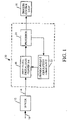
- FIG. 1 is a simplified block diagram of a transmitter 10 in accordance with one embodiment.
- Transmitter 10 in the embodiment shown in FIG. 1 , includes analog-to-digital (A/D) converter 18, processor 20 and programmable resolution component 22.
- Transmitter 10 is shown connected to sensor 12, which senses a process control parameter indicated by arrow 14.
- Transmitter 10 is also shown connected to a two wire process control loop 16, but it could be connected to a wireless transmission connection instead, or in addition.
- process control loop 16 provides power to transmitter 10.
- Processor 20 transmits information over process control loop 16 and receives information from other circuits or systems, over process control loop 16 as well.
- process control loop 16 may illustratively be a 4-20mA process control loop and may operate using a suitable communication protocol.
- process control loop 16 can be replaced by, or used in addition to, a wireless connection, transmitting the information wirelessly employing various wireless techniques or configurations.
- Sensor 12 is illustratively a process variable sensor that receives input 14 from a process being sensed.
- Sensor 12 may illustratively be a sensor for sensing pressure, temperature, pH, flow, etc.
- Sensor 12 illustratively provides an analog output 24, indicative of the sensed parameter, to A/D converter 18.
- sensor 12 will be described as a temperature sensor. However, any other suitable sensor can be used as well, and temperature is but one example of a variable or parameter that can be sensed.
- the output 24 from sensor 12 may illustratively be provided to a circuit (not shown) that amplifies and filters the analog sensor signal, as appropriate. This can be part of sensor 12, or a separate circuit. In any case, the amplified and filtered signal 24 is then provided to A/D converter 18.
- A/D converter 18 provides a digitized output to processor 20, which is a digital representation of the analog signal 24 provided by sensor 12.
- Processor 20 of course, illustratively has associated memory and clock circuitry, and provides information regarding the sensed parameter over process control loop 16.
- processor 20 can include an input/output (I/O) circuit, or an I/O circuit can be provided separately, that transmits information in a digital format on loop 16, or in an analog format by controlling current flow through loop 16. In any case, the information related to the sensed parameter is provided over process control loop 16 by transmitter 10.
- I/O input/output
- FIG. 2 is a graph illustrating a relationship between input voltage relative to a reference voltage and resolution of A/D converter 18.
- FIG. 2 shows that A/D converter 18 can provide an output in three different resolution zones.
- the resolution zones include a relatively high resolution zone, a medium resolution zone (which outputs the digital value with a resolution in volts per count that is lower resolution than the high resolution zone), and a relatively low resolution zone (which outputs the digital value with a resolution that is even lower resolution than the medium resolution zone).
- the particular resolution zone which A/D converter 18 is capable of operating in is, in one example, based on the signal level of the analog signal 24 and its relation to a reference voltage Vref used by A/D converter 18 in making its measurements. In the exemplary embodiment shown in FIG.
- A/D converter 18 can operate in the high resolution zone when signal 24 is between +Vref/3 and -Vref/3.
- A/D converter 18 can operate in the medium resolution zone when signal 24 is between +/-Vref/3 and +/-Vref/2, and A/D converter 18 can only operate in the low resolution zone when signal 24 is between +/-Vref/2 and +/-Vref.
- Vref/x the relationship shown in FIG. 2 and the particular values of Vref/x are examples only.
- A/D converter 18 was configured to operate in a fixed resolution zone that could accommodate the entire specified operating range of sensor 12. That is, if sensor 12 was capable of sensing a temperature and providing an output signal 24 between -Vref and +Vref/3, then A/D converter 18 would be configured to provide its output in the lowest resolution. This would be required in order to accommodate the full specified operating range of sensor 12.
- sensor 12 usually operates within a much narrower range, such as range 30 identified in FIG. 2 .
- A/D converter 18 set to a resolution zone that is the lowest resolution zone, results in unneeded resolution errors.
- the error due to not using the maximum possible resolution setting given the input signal becomes a significant factor in total system error.
- FIG. 1 shows that transmitter 10 also includes programmable resolution component 22.
- Programmable resolution component 22 provides an output to A/D converter 18 that changes the resolution setting of A/D converter 18.
- Component 22 is controlled by processor 20 based upon the value of the measured input signal 24. Therefore, as the value of signal 24 approaches the value corresponding to a new resolution zone (shown in FIG. 2 ) processor 20 dynamically adjusts the resolution of A/D converter 18 to match the new resolution zone.
- processor 20 controls component 22 to keep A/D converter 18 within the high resolution zone.
- processor 20 controls component 22 to dynamically adjust the resolution of A/D converter 18 so that it is in the medium resolution zone.
- processor 20 can control component 22 to dynamically adjust the resolution of A/D converter 18 again.
- the resolution setting of A/D converter 18 is always in an appropriate zone (in that it matches the best resolution obtainable given the input signal 24). This increases the overall resolution with which A/D converter 18 will provide its output to processor 20, over that of a system with one, fixed resolution setting.
- Transmitter 10 thus takes advantage of the relatively high resolution zones of A/D convert 18, even though the entire operating range of sensor 24 includes areas outside the high resolution zone. Yet, if the measured value 24 approaches a lower resolution zone, the resolution of A/D convert 18 is simply adjusted to match that zone.
- processor 20 uses a window of values around each boundary between resolution zones. As signal 24 enters the window, approaching a resolution zone boundary, processor 20 can change the resolution of A/D converter 18 either ahead of time, to accommodate the new zone, or processor 20 can wait until signal 24 actually crosses the boundary before changing the resolution. In another embodiment, processor 20 may also measure a rate of change of signal 24 as it approaches a boundary and use the rate of change to determine how quickly to change resolution as well. Similarly, processor 20 may implement a hysteresis band for the transitions between different resolution settings.
- the hysteresis will keep processor 20 from continuously changing the resolution setting of A/D converter 18 in an undesirable way.
- the size of a given window, or hysteresis band, or the particular rate of change used, may vary with the particular implementation. Of course, other modifications can be made as well.
- programmable resolution component 22 is shown as a separate component from A/D converter 18. However, some current A/D converters 18 have component 22 incorporated therein such that processor 20 can simply provide a control output to a resolution setting input of A/D converter 18.
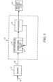
- FIG. 3 shows a simplified block diagram of such an embodiment.
- FIG. 3 The items shown in FIG. 3 are similar to those shown in FIG. 1 , and similar items are similarly numbered. However, it can be seen that instead of having a separate programmable resolution component 22 that is used to change the resolution of A/D converter 18, transmitter 10 is implemented with an A/D converter 18 that simply has a resolution setting input 40. Thus, processor 20 simply provides the resolution control output, for dynamically adjusting the resolution of A/D converter 18, to resolution setting input 40 of A/D converter 18. This changes the resolution setting of A/D converter 18.
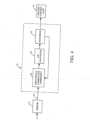
- FIG. 4 is a simplified block diagram of another transmitter 10 in accordance with yet another embodiment.
- transmitter 10 includes A/D converter 18 and processor 20.
- A/D converter 18 instead of A/D converter 18 having a resolution setting input (such as 40 shown in FIG. 3 ), transmitter 19 includes input signal normalizer component 42.
- A/D converter 18 has a high resolution zone centered around a particular input voltage measurement. For example only, it is assumed that A/D converter 18 operates with resolution zones such as those shown in FIG. 2 . Therefore, as long as input signal 24 is within +/-Vref/3 then A/D converter 18 can perform its conversion in the high resolution zone, using the highest resolution obtainable by the A/D converter 18.
- input signal normalizer component 42 normalizes input signal 24 to illustratively keep it within the high resolution region of A/D converter 18. That is, component 42 introduces an offset into signal 24 to keep it within the high resolution zone of A/D converter 18.
- FIG. 5A is a simplified diagram showing one embodiment of input signal normalizer component 42 in partial schematic form.
- sensor 12 includes, by way of example, resistive thermal device (RTD) 50 or thermocouple 52.
- RTD resistive thermal device
- component 42 includes a pair of switches 54 and 56 that are controlled by processor 20.
- Component 42 also includes a resistive network of resistors 58, 60, 62 and 64, along with Zener diode 66.
- component 42 effectively allows the zero point output by sensor 12 to be shifted down by a predetermined value. If the signal provided by sensor 12 is within an acceptable high resolution zone, then processor 20 operates switches 54 and 56 so that switch 54 is closed and switch 56 is opened, as shown in FIG. 5A . This causes sensor current I sensor to flow along a first path indicated by arrow 68. A/D converter 18 can perform the conversion and provide the measured, converted output to processor 20 with the highest resolution.
- processor 20 can control switches 54 and 56 as shown in FIG. 5B , such that switch 54 is open and switch 56 is closed. This causes the current Isensor to flow along a second path indicated by arrow 70. This effectively lowers the sensor input 0 point such that it is within the high resolution zone voltage window as shown in FIG. 2 .
- additional resistive dividers and switches can be added to accommodate other sensor ranges as well, and those shown are exemplary only.
- FIG. 6 is a simplified block diagram of yet another embodiment.
- transmitter 10 includes programmable reference voltage 80 that provides an input to the Vref input that is used as the reference voltage in A/D converter 18 for making the A/D conversions.
- Processor 20 controls programmable reference voltage 80 based on the measured value of the sensor input signal 24 so that A/D converter 18 can keep operating in a relatively high resolution zone.
- different voltage reference values provided to A/D converter 18 cause A/D converter 18 to make its conversions at different quantization levels.
- processor 20 can change the resolution level used by A/D converter 18.
- programmable reference voltage 80 is illustratively comprised of a plurality of different, selectable voltage taps that can be selected by processor 20. Each tap corresponds to a different voltage level that is provided, when selected, as the Vref input to A/D converter 18. In this way, processor 20 can dynamically adjust the quantization level (resolution) with which A/D converter 18 operates, based on the value of the measured input signal 24.
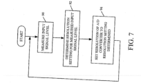
- FIG. 7 is a simplified flow diagram illustrating one embodiment of the operation of transmitter 10.
- transmitter 10 first measures the input signal level of sensor input 24. This is indicated by block 90.
- Processor 20 determines the appropriate resolution setting based on the measured sensor input signal level by determining which resolution zone signal 24 falls in. This is indicated by block 92.
- Processor 20 sets the resolution of A/D converter to the resolution setting that matches the resolution zone it determined in block 92. This is indicated by block 94.
- the particular way in which processor 20 controls transmitter 10 to dynamically adjust the resolution of A/D converter 18 will depend on the particular embodiment used for that adjustment. A number of exemplary embodiments are discussed above with respect to FIGS. 1-6 . It will be appreciated that FIG. 7 is but one exemplary method of operating transmitter 10.
Landscapes
- Engineering & Computer Science (AREA)
- Theoretical Computer Science (AREA)
- Analogue/Digital Conversion (AREA)
Abstract
Description
- The present invention relates to process variable transmitters used in process control and monitoring systems. More specifically, the present invention relates to dynamically adjusting an input to an analog-to-digital converter in such a system, in order to improve the resolution of the A/D measurement, during operation.
- Process variable transmitters are used to measure process parameters in a process control or monitoring system. Microprocessor-based transmitters often include a sensor, an analog-to-digital converter for converting an output from the sensor into a digital form, a microprocessor for compensating the digitized output, and an output circuit for transmitting the compensated output. Currently, this transmission is normally done over a process control loop, such as a 4-20mA control loop, or wirelessly.
- One exemplary parameter that is measured by such a system is temperature, which is sensed by measuring the resistance of a resistive temperature device (RTD, which is also sometimes called a platinum resistance thermometer or PRT) or the voltage output by a thermocouple. Of course, temperature is only exemplary, and a wide variety of other process control parameters can be measured as well.
- Some typical A/D converters are configured with a fixed voltage reference and a configurable resolution gain adjustment. Each gain setting for the configurable resolution gain adjustment corresponds to a reference point that is a scalar of the attached voltage reference. The voltage reference is used by the A/D converter to set the resolution (in volts per count) of the A/D converter. The resolution of the A/D converter can thus be changed based on an expected signal level of the analog input signal being measured.
- Conventional monitoring systems, in which A/D converters are implemented, often have the configurable resolution gain adjustment set so that the A/D converter can measure the full range of a specified sensor. That is, the configurable resolution gain adjustment is set for a single, fixed resolution which can accommodate the entire sensor range. However, the actual input signal may often have a value (or vary within a range of values) for which the A/D converter could be set to a much higher resolution. Thus, setting the gain adjustment to a set, fixed resolution results in a measurement circuit that is not tuned to use the full capability of the A/D converter.
- A process variable transmitter is used to measure a process variable, and, in doing so, dynamically changes the resolution of the A/D converter based upon the measured value of the analog input signal. This can be done by automatically adjusting the configurable resolution gain adjustment based on the value of the analog signal being measured, by normalizing the input signal being measured so that it is centered in an optimal resolution window of the A/D converter, or by adjusting a voltage reference provided to the A/D converter.
-
-
FIG. 1 is a simplified block diagram of a process variable transmitter coupled to a sensor. -
FIG. 2 is a graph of input voltage versus resolution. -
FIG. 3 is a simplified block diagram of the system shown inFIG. 1 , where the A/D converter has a configurable resolution setting. -
FIG. 4 is a simplified block diagram of one embodiment in which the input signal is normalized. -
FIGS. 5A and5B are schematic diagrams of one implementation for normalizing the input signal. -
FIG. 6 is a simplified block diagram of one embodiment of dynamically changing the A/D resolution by changing the voltage reference to the A/D converter. -
FIG. 7 is a simplified flow diagram illustrating one embodiment of the operation of the system. -
FIG. 1 is a simplified block diagram of atransmitter 10 in accordance with one embodiment.Transmitter 10, in the embodiment shown inFIG. 1 , includes analog-to-digital (A/D)converter 18,processor 20 andprogrammable resolution component 22.Transmitter 10 is shown connected tosensor 12, which senses a process control parameter indicated by arrow 14.Transmitter 10 is also shown connected to a two wireprocess control loop 16, but it could be connected to a wireless transmission connection instead, or in addition. In one embodiment,process control loop 16 provides power totransmitter 10.Processor 20 transmits information overprocess control loop 16 and receives information from other circuits or systems, overprocess control loop 16 as well. By way of example,process control loop 16 may illustratively be a 4-20mA process control loop and may operate using a suitable communication protocol. Alternatively,process control loop 16 can be replaced by, or used in addition to, a wireless connection, transmitting the information wirelessly employing various wireless techniques or configurations. -
Sensor 12 is illustratively a process variable sensor that receives input 14 from a process being sensed.Sensor 12 may illustratively be a sensor for sensing pressure, temperature, pH, flow, etc.Sensor 12 illustratively provides ananalog output 24, indicative of the sensed parameter, to A/D converter 18. - In the present description,
sensor 12 will be described as a temperature sensor. However, any other suitable sensor can be used as well, and temperature is but one example of a variable or parameter that can be sensed. - It should be noted that the
output 24 fromsensor 12 may illustratively be provided to a circuit (not shown) that amplifies and filters the analog sensor signal, as appropriate. This can be part ofsensor 12, or a separate circuit. In any case, the amplified and filteredsignal 24 is then provided to A/D converter 18. A/D converter 18 provides a digitized output toprocessor 20, which is a digital representation of theanalog signal 24 provided bysensor 12.Processor 20, of course, illustratively has associated memory and clock circuitry, and provides information regarding the sensed parameter overprocess control loop 16. It should be noted thatprocessor 20 can include an input/output (I/O) circuit, or an I/O circuit can be provided separately, that transmits information in a digital format onloop 16, or in an analog format by controlling current flow throughloop 16. In any case, the information related to the sensed parameter is provided overprocess control loop 16 bytransmitter 10. -
FIG. 2 is a graph illustrating a relationship between input voltage relative to a reference voltage and resolution of A/D converter 18.FIG. 2 shows that A/D converter 18 can provide an output in three different resolution zones. The resolution zones include a relatively high resolution zone, a medium resolution zone (which outputs the digital value with a resolution in volts per count that is lower resolution than the high resolution zone), and a relatively low resolution zone (which outputs the digital value with a resolution that is even lower resolution than the medium resolution zone). The particular resolution zone which A/D converter 18 is capable of operating in is, in one example, based on the signal level of theanalog signal 24 and its relation to a reference voltage Vref used by A/D converter 18 in making its measurements. In the exemplary embodiment shown inFIG. 2 , A/D converter 18 can operate in the high resolution zone whensignal 24 is between +Vref/3 and -Vref/3. A/D converter 18 can operate in the medium resolution zone whensignal 24 is between +/-Vref/3 and +/-Vref/2, and A/D converter 18 can only operate in the low resolution zone whensignal 24 is between +/-Vref/2 and +/-Vref. Of course, the relationship shown inFIG. 2 and the particular values of Vref/x are examples only. - In many prior systems, A/
D converter 18 was configured to operate in a fixed resolution zone that could accommodate the entire specified operating range ofsensor 12. That is, ifsensor 12 was capable of sensing a temperature and providing anoutput signal 24 between -Vref and +Vref/3, then A/D converter 18 would be configured to provide its output in the lowest resolution. This would be required in order to accommodate the full specified operating range ofsensor 12. - However, it may happen that
sensor 12 usually operates within a much narrower range, such asrange 30 identified inFIG. 2 . In that case, having A/D converter 18 set to a resolution zone that is the lowest resolution zone, results in unneeded resolution errors. As device accuracy specifications are tightened, the error due to not using the maximum possible resolution setting given the input signal becomes a significant factor in total system error. - Therefore,
FIG. 1 shows thattransmitter 10 also includesprogrammable resolution component 22.Programmable resolution component 22 provides an output to A/D converter 18 that changes the resolution setting of A/D converter 18.Component 22 is controlled byprocessor 20 based upon the value of the measuredinput signal 24. Therefore, as the value ofsignal 24 approaches the value corresponding to a new resolution zone (shown inFIG. 2 )processor 20 dynamically adjusts the resolution of A/D converter 18 to match the new resolution zone. Thus, assensor 12 is providing anoutput 24 within range 30 (shown inFIG. 2 )processor 20controls component 22 to keep A/D converter 18 within the high resolution zone. - However, as the
output signal 24 provided bysensor 12 approaches either of the medium resolution zones on either side of the high resolution zone (again shown inFIG. 2 )processor 20controls component 22 to dynamically adjust the resolution of A/D converter 18 so that it is in the medium resolution zone. Similarly, assignal 24 moves toward another zone,processor 20 can controlcomponent 22 to dynamically adjust the resolution of A/D converter 18 again. Thus, the resolution setting of A/D converter 18 is always in an appropriate zone (in that it matches the best resolution obtainable given the input signal 24). This increases the overall resolution with which A/D converter 18 will provide its output toprocessor 20, over that of a system with one, fixed resolution setting.Transmitter 10 thus takes advantage of the relatively high resolution zones of A/D convert 18, even though the entire operating range ofsensor 24 includes areas outside the high resolution zone. Yet, if the measuredvalue 24 approaches a lower resolution zone, the resolution of A/D convert 18 is simply adjusted to match that zone. - In one embodiment,
processor 20 uses a window of values around each boundary between resolution zones. Assignal 24 enters the window, approaching a resolution zone boundary,processor 20 can change the resolution of A/D converter 18 either ahead of time, to accommodate the new zone, orprocessor 20 can wait untilsignal 24 actually crosses the boundary before changing the resolution. In another embodiment,processor 20 may also measure a rate of change ofsignal 24 as it approaches a boundary and use the rate of change to determine how quickly to change resolution as well. Similarly,processor 20 may implement a hysteresis band for the transitions between different resolution settings. Therefore, if the measuredsensor input signal 24 is hovering around a transition region that transitions from one resolution setting to the next, the hysteresis will keepprocessor 20 from continuously changing the resolution setting of A/D converter 18 in an undesirable way. The size of a given window, or hysteresis band, or the particular rate of change used, may vary with the particular implementation. Of course, other modifications can be made as well. - It should be noted that, for purposes of the description of
FIG. 1 ,programmable resolution component 22 is shown as a separate component from A/D converter 18. However, some current A/D converters 18 havecomponent 22 incorporated therein such thatprocessor 20 can simply provide a control output to a resolution setting input of A/D converter 18.FIG. 3 shows a simplified block diagram of such an embodiment. - The items shown in
FIG. 3 are similar to those shown inFIG. 1 , and similar items are similarly numbered. However, it can be seen that instead of having a separateprogrammable resolution component 22 that is used to change the resolution of A/D converter 18,transmitter 10 is implemented with an A/D converter 18 that simply has aresolution setting input 40. Thus,processor 20 simply provides the resolution control output, for dynamically adjusting the resolution of A/D converter 18, toresolution setting input 40 of A/D converter 18. This changes the resolution setting of A/D converter 18. -
FIG. 4 is a simplified block diagram of anothertransmitter 10 in accordance with yet another embodiment. In the embodiment shown inFIG. 4 ,transmitter 10 includes A/D converter 18 andprocessor 20. However, instead of A/D converter 18 having a resolution setting input (such as 40 shown inFIG. 3 ), transmitter 19 includes inputsignal normalizer component 42. - In the embodiment shown in
FIG. 4 , A/D converter 18 has a high resolution zone centered around a particular input voltage measurement. For example only, it is assumed that A/D converter 18 operates with resolution zones such as those shown inFIG. 2 . Therefore, as long asinput signal 24 is within +/-Vref/3 then A/D converter 18 can perform its conversion in the high resolution zone, using the highest resolution obtainable by the A/D converter 18. Instead of resetting the resolution of A/D converter 18, inputsignal normalizer component 42 normalizesinput signal 24 to illustratively keep it within the high resolution region of A/D converter 18. That is,component 42 introduces an offset intosignal 24 to keep it within the high resolution zone of A/D converter 18. -
FIG. 5A is a simplified diagram showing one embodiment of inputsignal normalizer component 42 in partial schematic form.FIG. 5A also shows thatsensor 12 includes, by way of example, resistive thermal device (RTD) 50 orthermocouple 52. In the embodiment shown inFIG. 5A ,component 42 includes a pair ofswitches processor 20.Component 42 also includes a resistive network ofresistors Zener diode 66. - In the embodiment shown in
FIG. 5A ,component 42 effectively allows the zero point output bysensor 12 to be shifted down by a predetermined value. If the signal provided bysensor 12 is within an acceptable high resolution zone, thenprocessor 20 operatesswitches switch 54 is closed and switch 56 is opened, as shown inFIG. 5A . This causes sensor current Isensor to flow along a first path indicated byarrow 68. A/D converter 18 can perform the conversion and provide the measured, converted output toprocessor 20 with the highest resolution. - However, in the event that the signal output by
sensor 12 to A/D converter 18 moves toward a lower resolution zone, thenprocessor 20 can controlswitches FIG. 5B , such thatswitch 54 is open and switch 56 is closed. This causes the current Isensor to flow along a second path indicated byarrow 70. This effectively lowers the sensor input 0 point such that it is within the high resolution zone voltage window as shown inFIG. 2 . Of course, it will be noted that additional resistive dividers and switches can be added to accommodate other sensor ranges as well, and those shown are exemplary only. -
FIG. 6 is a simplified block diagram of yet another embodiment. InFIG. 6 , similar items to those shown in previous figures are similarly numbered.FIG. 6 illustrates an embodiment in which A/D converter 18 does not provide any means to select a different resolution gain for its measurements. In that case,transmitter 10 includesprogrammable reference voltage 80 that provides an input to the Vref input that is used as the reference voltage in A/D converter 18 for making the A/D conversions.Processor 20 controlsprogrammable reference voltage 80 based on the measured value of thesensor input signal 24 so that A/D converter 18 can keep operating in a relatively high resolution zone. In the embodiment, different voltage reference values provided to A/D converter 18 cause A/D converter 18 to make its conversions at different quantization levels. Thus, by changing Vref,processor 20 can change the resolution level used by A/D converter 18. - Therefore, in the embodiment shown in
FIG. 6 ,programmable reference voltage 80 is illustratively comprised of a plurality of different, selectable voltage taps that can be selected byprocessor 20. Each tap corresponds to a different voltage level that is provided, when selected, as the Vref input to A/D converter 18. In this way,processor 20 can dynamically adjust the quantization level (resolution) with which A/D converter 18 operates, based on the value of the measuredinput signal 24. -
FIG. 7 is a simplified flow diagram illustrating one embodiment of the operation oftransmitter 10. In the embodiment shown inFIG. 7 ,transmitter 10 first measures the input signal level ofsensor input 24. This is indicated byblock 90.Processor 20 then determines the appropriate resolution setting based on the measured sensor input signal level by determining whichresolution zone signal 24 falls in. This is indicated byblock 92.Processor 20 then sets the resolution of A/D converter to the resolution setting that matches the resolution zone it determined inblock 92. This is indicated byblock 94. The particular way in whichprocessor 20controls transmitter 10 to dynamically adjust the resolution of A/D converter 18 will depend on the particular embodiment used for that adjustment. A number of exemplary embodiments are discussed above with respect toFIGS. 1-6 . It will be appreciated thatFIG. 7 is but one exemplary method of operatingtransmitter 10. - Although the present invention has been described with reference to preferred embodiments, workers skilled in the art will recognize that changes may be made in form and detail without departing from the spirit and scope of the invention.
-
- 1. A method of controlling an analog-to-digital (A/D) converter in a process variable transmitter that converts an analog input signal indicative of an industrial process variable to a digital output signal, the method comprising:
- receiving the analog input signal indicative of the industrial process variable;
- measuring a signal level of the analog input signal;
- intermittently matching a resolution setting for the A/D converter to the measured signal level for the analog input, based on the measured signal level for the analog input signal, such that the A/D converter converts the analog input signal to the digital output signal with a highest resolution obtainable from the A/D converter, given the measured signal level of the analog input signal;
- converting the analog input signal to the digital output signal using the matched resolution setting; and
- sending information related to the industrial process variable over a transmission connection.
- 2. The method of
embodiment 1 wherein the highest resolution obtainable from the A/D converter changes as the measured level of the analog input signal varies among a plurality of different signal ranges, and wherein intermittently matching comprises:- measuring the signal level of the analog input signal; and
- if the measured signal level crosses a threshold corresponding to a boundary between one of the plurality of different signal ranges and another of the plurality of different signal ranges, changing the resolution setting for the A/D converter to correspond to the other of the plurality of different signal ranges.
- 3. The method of
embodiment 2 wherein changing the resolution setting is performed using hysteresis such that the resolution setting is only changed if the measured signal level crosses the threshold by a predetermined amount. - 4. The method of
embodiment 2 wherein the resolution setting for the A/D converter comprises an adjustable gain setting that sets a resolution set-point to be indicative of a portion of a voltage reference potential input to the A/D converter, and wherein intermittently matching the resolution setting comprises:
intermittently changing the adjustable gain setting to vary the resolution set-point based on the measured level of the analog input signal. - 5. The method of
embodiment 2 wherein the resolution of the A/D converter changes based on a reference voltage applied to the A/D converter and wherein changing the resolution setting comprises:
changing the reference voltage applied to the A/D converter. - 6. The method of
embodiment 1 wherein the highest resolution obtainable from the A/D converter changes as the measured level of the analog input signal varies among a plurality of different signal ranges, and wherein intermittently matching comprises:- measuring the signal level of the analog input signal; and
- if the measured signal level crosses a threshold corresponding to a boundary between a higher resolution range of the plurality of different signal ranges and a lower resolution range of the plurality of different signal ranges, introducing a signal offset into the signal level of the analog input signal to keep the measured signal level in the higher resolution range.
- 7. The method of
embodiment 1 wherein intermittently matching comprises:
determining whether the measured signal level has entered a window around a boundary between one of the plurality of different signal ranges and another of the plurality of different signal ranges. - 8. The method of embodiment 7 wherein intermittently matching comprises:
changing the resolution setting for the A/D converter to correspond to the other of the plurality of different signal ranges even if the measured signal level is still within the one of the plurality of different signal ranges, as long as the measured signal level has entered the window. - 9. The method of embodiment 8 wherein changing the resolution setting comprises:
changing the resolution setting for the A/D converter to correspond to the other of the plurality of different signal ranges, even if the measured signal level is still within the one of the plurality of different signal ranges, as long as the measured signal level has entered the window and is approaching the other of the plurality of different signal ranges. - 10. The method of embodiment 9 and further comprising:
- measuring a rate of change of the measured signal level; and
- changing the resolution setting for the A/D converter to correspond to the other of the plurality of different signal ranges more quickly if the rate of change of the measured signal level is at a first, higher rate, than if the rate of change of the measured signal level is at a second, lower rate.
- 11. A process variable transmitter that receives a sensor input signal from a sensor that senses a process variable and provides the sensor input signal at an analog signal level indicative of the process variable, comprising:
- an analog-to-digital (A/D) converter that converts the sensor input signal to a digital value at a resolution, wherein the resolution obtainable by the A/D converter changes according to a predetermined relationship between the analog signal level of the sensor input signal and a reference voltage provided to the A/D converter; and
- a processor, coupled to the A/D converter, receiving the digital value and transmitting information over a process control loop based on the digital value, the processor providing a resolution control signal to control the resolution at which the A/D converter provides the digital value by changing at least one of the analog signal level of the sensor input signal or the reference voltage, to match the resolution to the analog signal level of the sensor input signal so the A/D converter provides the digital value at a predetermined resolution, given the analog signal level of the sensor input signal.
- 12. The process variable transmitter of embodiment 11 wherein the A/D converter includes an adjustable gain setting that sets a resolution of the A/D converter based a portion of the reference voltage input to the A/D converter.
- 13. The process variable transmitter of
embodiment 12 wherein the processor matches the resolution to the analog signal level by changing the adjustable gain setting to vary the resolution based on the measured level of the analog input signal. - 14. The process variable transmitter of embodiment 11 wherein the reference voltage provided to the A/D converter is programmable by the processor and wherein the processor matches the resolution to the sensor input signal by programming a given reference voltage to obtain a given resolution based on the digital value of the sensor input signal.
- 15. The process variable transmitter of embodiment 11 and further comprising:
an input signal normalizer component, coupled to the processor and the sensor, that introduces an offset into the analog signal level of the sensor input signal. - 16. The process variable transmitter of embodiment 15 wherein the processor controls the input signal normalizer component to introduce the offset into the analog signal level of the sensor input signal when introduction of the offset increases the resolution of the A/D converter over a resolution of the A/D converter without the offset introduced into the analog signal level.
- 17. The process variable of embodiment 11 wherein the processor matches the resolution to the analog signal level of the sensor input signal so the A/D converter provides the digital value at a highest possible resolution, given the analog signal level of the sensor input signal.
- 18. The process variable of embodiment 11 wherein the processor matches the resolution to the analog signal level of the sensor input signal so the A/D converter provides the digital value at a highest possible resolution, given the analog signal level of the sensor input signal, each time the A/D converter converts the sensor input signal to a digital value.
- 19. A method of controlling a process variable transmitter, the method comprising:
- receiving, from a sensor, an analog input signal indicative of an industrial process variable;
- measuring a signal level of the analog input signal by using an analog-to-digital (A/D) converter that converts the analog input signal to a digital output signal;
- varying a resolution setting for the A/D converter, based on the measured signal level for the analog input, to configure the A/D converter to convert the analog input signal to the digital output signal with a highest resolution obtainable from the A/D converter, given the measured signal level of the analog input signal;
- converting the analog input signal to the digital output signal using the varied resolution setting; and
- sending information related to the industrial process variable over a transmission connection comprising one of a hardwired process control loop and a wireless connection.
- 20. The method of embodiment 19 wherein varying a resolution setting comprises:
automatically changing a signal level of the analog input signal by a predetermined amount based on the measured signal level for the analog input signal.
Claims (25)
- A method of controlling an analog-to-digital (A/D) converter (18) for transmitting a process variable that converts an analog input signal received from a sensor (12) to a digital output signal, the method comprising:a) receiving the analog input signal;b) measuring a signal level variation (30) of the analog input signal using the A/D converter (18) and a processor (20);c) intermittently matching a resolution setting for the A/D converter (18) to the measured signal level variation for the analog input from among a plurality of resolution settings, by a programmable resolution component (22);d) wherein the programmable resolution component (22) is controlled by the processor (20), based on the measured signal level variation for the analog input signal ;e) converting the analog input signal to the digital output signal using the matched resolution setting and a reference voltage (Vref) used by the A/D converter; andf) sending information related to the industrial process variable over a transmission connection;g1) wherein the resolution obtainable from the A/D converter (18) changes as the measured level of the analog input signal varies among a plurality of different input signal ranges ([-Vref/3, +Vref/3]; [+Vref/3, +Vref/2], [-Vref/3, -Verf/2]; [+Vref/2, Vref], [-Vref/2, - Vref]) relative to the reference voltage; such thatg2) the particular resolution zone which the A/D converter (18) is capable of operating in is based on the signal level variation of the analog signal (24) and its relation to the reference voltage (Vref) used by A/D converter (18).
- The method of claim 1, wherein the different input signal ranges are defined as [-Vref/3, +Vref/3]; [+Vref/3, +Vref/2], [-Vref/3, -Verf/2]; and [+Vref/2, Vref], [-Vref/2, - Vref]), andg3) wherein the A/D converter 18 is capable to operate in a high resolution zone when the input signal (24) is between +Vref/3 and -Vref/3, to operate in a medium resolution zone when the input signal (24) is between +/-Vref/3 and +/-Vref/2, and to operate in a low resolution zone when the input signal (24) is between +/-Vref/2 and +/-Vref; whereing4) if the input signal (24) enters a lower resolution zone, the resolution of the A/D converter (18) is adjusted to match that zone.
- The method of claim 1 or 2, wherein
g5) when the measured level of the analog input signal varies within a first input level range (0, -Vref/3; 0, +Vref/3), the A/D converter (18) operates at a first predetermined high resolution, when the measured level of the analog input signal varies within a second input level range (-Vref/3, -Vref/2; +Vref/3, +Vref/2) larger than the first range, the A/D converter (18) operates at a second predetermined medium resolution, the second medium resolution being smaller than the first high resolution, and when the measured level of the analog input signal varies within a third input level range (-Vref/2, -Vref/; +Vref,/2 Vref) larger than the first range, the A/D converter (18) operates at a third predetermined low resolution, the third medium resolution being smaller than the second medium resolution. - The method of claim 1, wherein intermittently matching comprises:measuring the signal level of the analog input signal; andif the measured signal level crosses a threshold corresponding to a boundary between one of the plurality of different signal ranges and another of the plurality of different signal ranges, changing the resolution setting for the A/D converter (18) to correspond to the other of the plurality of different signal ranges.
- The method of claim 4, wherein changing the resolution setting is performed using hysteresis such that the resolution setting is only changed if the measured signal level crosses the threshold by a predetermined amount.
- The method of claim 4, wherein the resolution setting for the A/D converter (18) comprises an adjustable gain setting that sets a resolution set-point to be indicative of a portion of a voltage reference potential input to the A/D converter (18), and
wherein intermittently matching the resolution setting comprises:
intermittently changing the adjustable gain setting to vary the resolution set-point based on the measured level of the analog input signal. - The method of claim 4, wherein the resolution of the A/D converter (18) changes based on a reference voltage applied to the A/D converter (18) and wherein changing the resolution setting comprises:
changing the reference voltage applied to the A/D converter (18). - The method of claim 1, wherein the high resolution obtainable from the A/D converter (18) changes as the measured level of the analog input signal varies among a plurality of different signal ranges corresponding to the plurality of resolution settings, and wherein intermittently matching comprises:measuring the signal level of the analog input signal; andif the measured signal level crosses a threshold corresponding to a boundary between a higher resolution range of the plurality of different signal ranges and a lower resolution range of the plurality of different signal ranges, introducing a signal offset into the signal level of the analog input signal to keep the measured signal level in the higher resolution range.
- The method of claim 1, wherein intermittently matching comprises:
determining whether the measured signal level has entered a window around a boundary between one of the plurality of different signal ranges and another of the plurality of different signal ranges. - The method of claim 9, wherein intermittently matching comprises:
changing the resolution setting for the A/D converter (18) to correspond to the other of the plurality of different signal ranges even if the measured signal level is still within the one of the plurality of different signal ranges, as long as the measured signal level has entered the window. - The method of claim 10, wherein changing the resolution setting comprises:
changing the resolution setting for the A/D converter (18) to correspond to the other of the plurality of different signal ranges, even if the measured signal level is still within the one of the plurality of different signal ranges, as long as the measured signal level has entered the window and is approaching the other of the plurality of different signal ranges. - The method of claim 11, further comprising:measuring a rate of change of the measured signal level; andchanging the resolution setting for the A/D converter (18) to correspond to the other of the plurality of different signal ranges more quickly if the rate of change of the measured signal level is at a first, higher rate, than if the rate of change of the measured signal level is at a second, lower rate.
- The method according to claim 4, wherein the processor (20) uses a window of values around each boundary between one of the plurality of different signal ranges and another of the plurality of different signal ranges and when the signal level enters the window, approaching the boundary, the processor (20) changes the resolution of the A/D converter (18) either ahead of time or the processor (20) waits until the signal level crosses the boundary before changing the resolution.
- The method according to claim 4, wherein the processor (20) measures the rate of change of the signal level as it approaches the boundary between one of the plurality of different signal ranges and another of the plurality of different signal ranges, wherein the rate of change determines a width of a window or a time period before crossing the boundary at which the resolution is changed.
- A process variable transmitter (10) for receiving a sensor input signal from a sensor, comprising:a) an analog-to-digital (A/D) converter (18) that converts the sensor input signal to a digital value at a resolution, wherein the resolution obtainable by the A/D converter (18) changes according to a predetermined relationship between the analog signal level of the sensor input signal and a reference voltage provided to the A/D converter (18); andb) a processor (20), coupled to the A/D converter (18), receiving the digital value and transmitting information over a process control loop based on the digital value, the processor (20) providing a resolution control signal to control the resolution at which the A/D converter (18) provides the digital value by changing at least one of the analog signal level of the sensor input signal or the reference voltage, to match the resolution to the analog signal level of the sensor input signal so the A/D converter (18) provides the digital value at a predetermined resolution, given the analog signal level of the sensor input signal,c) wherein said matching is performed by a programable resolution component (22),d) wherein the programable resolution component (22) is controlled by the processor (20) based on the measured signal level variation for the analog signal level;e) wherein the A/D converter (18) includes an adjustable gain setting;f) the adjustable gain setting adapted to set a resolution of the A/D converter (18) based a portion of the reference voltage input to the A/D converter (18);g1) wherein the resolution obtainable from the A/D converter (18) changes as the measured level of the analog input signal varies among a plurality of different input signal ranges ([-Vref/3, +Vref/3]; [+Vref/3, +Vref/2], [-Vref/3, -Verf/2]; [+Vref/2, Vref], [-Vref/2, - Vref]) relative to the reference voltage; such thatg2) the particular resolution zone which the A/D converter (18) is capable of operating in is based on the signal level variation of the analog signal (24) and its relation to the reference voltage (Vref) used by A/D converter (18).
- The variable process transmitter of claim 14 or 15, wherein the different input signal ranges are defined as [-Vref/3, +Vref/3]; [+Vref/3, +Vref/2], [-Vref/3, -Verf/2]; and [+Vref/2, Vref], [-Vref/2, -Vref]), andg3) wherein the A/D converter (18) is capable to operate in a high resolution zone when the input signal (24) is between +Vref/3 and -Vref/3, to operate in a medium resolution zone when the input signal (24) is between +/-Vref/3 and +/-Vref/2, and to operate in a low resolution zone when the input signal (24) is between +/-Vref/2 and +/-Vref; whereing4) if the input signal (24) enters a lower resolution zone, the resolution of the A/D converter (18) is adjusted to match that zone.
- The process variable transmitter (10) of claim 15, wherein
e) when the measured level of the analog input signal varies within a first input level range (0, -Vref/3; 0, +Vref/3), the A/D converter (18) operates at a first predetermined high resolution, when the measured level of the analog input signal varies within a second input level range (-Vref/3, -Vref/2; +Vref/3, +Vref/2) larger than the first range, the A/D converter (18) operates at a second predetermined medium resolution, the second medium resolution being smaller than the first high resolution, and when the measured level of the analog input signal varies within a third input level range (-Vref/2, -Vref/; +Vref,/2 Vref) larger than the first range, the A/D converter (18) operates at a third predetermined low resolution, the third medium resolution being smaller than the second medium resolution. - The process variable transmitter (10) of claim 15, wherein the processor (20) matches the resolution to the analog signal level by changing the adjustable gain setting to vary the resolution based on the measured level of the analog input signal.
- The process variable transmitter (10) of claim 15, wherein the reference voltage provided to the A/D converter (18) is programmable by the processor (20) and wherein the processor (20) matches the resolution to the sensor input signal by programming a given reference voltage to obtain a given resolution based on the digital value of the sensor input signal.
- The process variable transmitter (10) of claim 15, and further comprising:
an input signal normalizer component, coupled to the processor (20) and the sensor, that introduces an offset into the analog signal level of the sensor input signal. - The process variable transmitter (10) of claim 20, wherein the processor (20) controls the input signal normalizer component to introduce the offset into the analog signal level of the sensor input signal when introduction of the offset increases the resolution of the A/D converter (18) over a resolution of the A/D converter (18) without the offset introduced into the analog signal level.
- The process variable transmitter (10) of claim 15, wherein the processor (20) matches the resolution to the analog signal level of the sensor input signal so the A/D converter (18) provides the digital value at a high resolution, given the analog signal level of the sensor input signal.
- The process variable transmitter (10) of claim 15, wherein the processor (20) matches the resolution to the analog signal level of the sensor input signal so the A/D converter (18) provides the digital value at a high resolution, given the analog signal level of the sensor input signal, each time the A/D converter (18) converts the sensor input signal to a digital value.
- A combination of the process variable transmitter according to claim 20 and a sensor (12), wherein the input signal normaliser (42) includes a pair of switches (54, 56) controlled by the processor (20) and a resistive network of resistors (58, 60, 62 and 64), along with a Zener diode (66),
wherein the sensor (12) comprises a resistive thermal device, RTD, (50) or thermocouple, TC, (52) having two terminals connected to the A/D converter, wherein a series connection of a first resistor (62) and a second resistor (64) is connected in parallel to the Zener diode (66), one end of a first switch (54) is connected to a first terminal of the RDT or TC and a second end of the first switch (54) is in a series connection connected to one end of a third resistor (58) the other end of which is connected to the cathode of the Zener diode (66) the anode of which is connected to grounded, and one end of a second switch (56), which at its second end is in a series connection connected to one end of a fourth resistor (60), is connected to the first terminal of the RTD (50) or the TC (52), and the second end of the fourth resistor (60) is connected to the series connection point between the first and second resistor (62, 64). - The combination according to claim 24, whereinif the signal provided by RTD (50) or the TC (52) is within an acceptable high resolution zone, then the processor (20) operates the first and second switch (54, 56) such that the first switch (54) is closed and the second switch (56) is opened such that this causes sensor current (ISENSOR) to flow along a first path through the first switch (54), the third resistor (58) and the Zener diode (66), wherein the A/D converter (18) performs conversion and provides the measured, converted output to processor (20) with the highest resolution; andif the signal provided by RTD (50) or the TC (52) moves towards a lower resolution zone, then the processor (20) operates the first and second switch (54, 56) such that the first switch (54) is opened and the second switch (56) is closed such that this causes sensor current (ISENSOR) to flow along a second path through the second switch (54), the fourth resistor (60) and the second resistor (64) to lower the RTD (50) or TC (52) 0 point.
Applications Claiming Priority (3)
| Application Number | Priority Date | Filing Date | Title |
|---|---|---|---|
| US13/077,132 US8378872B2 (en) | 2011-03-31 | 2011-03-31 | Dynamically adjusted A/D resolution |
| EP12714879.9A EP2692061A1 (en) | 2011-03-31 | 2012-03-07 | Dynamically adjusted a/d resolution |
| PCT/US2012/027962 WO2012134738A1 (en) | 2011-03-31 | 2012-03-07 | Dynamically adjusted a/d resolution |
Related Parent Applications (1)
| Application Number | Title | Priority Date | Filing Date |
|---|---|---|---|
| EP12714879.9A Division EP2692061A1 (en) | 2011-03-31 | 2012-03-07 | Dynamically adjusted a/d resolution |
Publications (1)
| Publication Number | Publication Date |
|---|---|
| EP4138304A1 true EP4138304A1 (en) | 2023-02-22 |
Family
ID=45974494
Family Applications (2)
| Application Number | Title | Priority Date | Filing Date |
|---|---|---|---|
| EP22180692.0A Pending EP4138304A1 (en) | 2011-03-31 | 2012-03-07 | Dynamically adjusted a/d resolution |
| EP12714879.9A Ceased EP2692061A1 (en) | 2011-03-31 | 2012-03-07 | Dynamically adjusted a/d resolution |
Family Applications After (1)
| Application Number | Title | Priority Date | Filing Date |
|---|---|---|---|
| EP12714879.9A Ceased EP2692061A1 (en) | 2011-03-31 | 2012-03-07 | Dynamically adjusted a/d resolution |
Country Status (8)
| Country | Link |
|---|---|
| US (2) | US8378872B2 (en) |
| EP (2) | EP4138304A1 (en) |
| JP (2) | JP5974077B2 (en) |
| CN (3) | CN102739255B (en) |
| AU (1) | AU2012238067B2 (en) |
| CA (1) | CA2830218C (en) |
| RU (1) | RU2568311C2 (en) |
| WO (1) | WO2012134738A1 (en) |
Families Citing this family (17)
| Publication number | Priority date | Publication date | Assignee | Title |
|---|---|---|---|---|
| US8864378B2 (en) * | 2010-06-07 | 2014-10-21 | Rosemount Inc. | Process variable transmitter with thermocouple polarity detection |
| US9207670B2 (en) | 2011-03-21 | 2015-12-08 | Rosemount Inc. | Degrading sensor detection implemented within a transmitter |
| US8378872B2 (en) | 2011-03-31 | 2013-02-19 | Rosemount Inc. | Dynamically adjusted A/D resolution |
| US9207129B2 (en) * | 2012-09-27 | 2015-12-08 | Rosemount Inc. | Process variable transmitter with EMF detection and correction |
| US9602122B2 (en) | 2012-09-28 | 2017-03-21 | Rosemount Inc. | Process variable measurement noise diagnostic |
| EP2778619B1 (en) * | 2013-03-15 | 2015-12-02 | Invensys Systems, Inc. | Process variable transmitter |
| DE102013223021A1 (en) * | 2013-11-12 | 2015-05-13 | Msa Europe Gmbh | Device for fault detection and / or identification of at least one sensor device |
| KR101722465B1 (en) * | 2015-08-26 | 2017-04-03 | 베이스코리아아이씨(주) | Removal sensor module of output sensor identification using one pin, apparatus and method of recognizing sensor of the removal sensor module using one pin |
| JP6436022B2 (en) * | 2015-09-03 | 2018-12-12 | 株式会社デンソー | A / D converter |
| CN107196656B (en) * | 2016-03-15 | 2020-11-06 | 联发科技(新加坡)私人有限公司 | A kind of signal calibration circuit and signal calibration method |
| US9774343B1 (en) * | 2016-07-13 | 2017-09-26 | The Boeing Company | Method and apparatus for improving the resolution of digitally sampled analog data |
| JP6714462B2 (en) * | 2016-07-29 | 2020-06-24 | 株式会社日立製作所 | Wireless sensor terminal, wireless sensor system, and sensor data collection method |
| EP3382406A1 (en) * | 2017-03-30 | 2018-10-03 | NorthQ ApS | A system and a method for estimation of current transported in a cable |
| US10453791B2 (en) | 2018-02-06 | 2019-10-22 | Apple Inc. | Metal-on-metal capacitors |
| US10284218B1 (en) | 2018-04-27 | 2019-05-07 | Hewlett Packard Enterprise Development Lp | Voltage window |
| CN112945454A (en) * | 2019-12-11 | 2021-06-11 | 安普泰科电子韩国有限公司 | Pressure sensing device and processing method thereof |
| WO2022146474A1 (en) * | 2021-01-04 | 2022-07-07 | Zeku, Inc. | Apparatus and method of configurable reduction to signal resolution |
Citations (5)
| Publication number | Priority date | Publication date | Assignee | Title |
|---|---|---|---|---|
| US6373423B1 (en) * | 1999-12-14 | 2002-04-16 | National Instruments Corporation | Flash analog-to-digital conversion system and method with reduced comparators |
| US6690312B1 (en) * | 1999-04-22 | 2004-02-10 | Siemens Aktiengesellschaft | Method and circuit for regulating the signal level fed to an analog/digital converter |
| US6784820B1 (en) * | 2003-04-09 | 2004-08-31 | Raytheon Company | High resolution, high dynamic range analog-to-digital converter system and related techniques |
| US20040189498A1 (en) * | 2003-02-28 | 2004-09-30 | Toshihiko Takahashi | Digital equalization apparatus |
| US20080100485A1 (en) * | 2006-10-27 | 2008-05-01 | Oki Electric Industry Co., Ltd. | Ofdm receiver |
Family Cites Families (32)
| Publication number | Priority date | Publication date | Assignee | Title |
|---|---|---|---|---|
| US5194865A (en) * | 1991-12-06 | 1993-03-16 | Interbold | Analog-to-digital converter circuit having automatic range control |
| US5329818A (en) | 1992-05-28 | 1994-07-19 | Rosemount Inc. | Correction of a pressure indication in a pressure transducer due to variations of an environmental condition |
| GB2287224B (en) * | 1994-03-02 | 1997-08-13 | Tohoku Ricoh Co Limited | Control device for a thermosensitive stencil printer |
| US5546082A (en) | 1994-04-22 | 1996-08-13 | Rosemount Analytical Inc. | Measurement probe with improved analog-to-digital conversion |
| US5669713A (en) | 1994-09-27 | 1997-09-23 | Rosemount Inc. | Calibration of process control temperature transmitter |
| US5621406A (en) | 1994-09-29 | 1997-04-15 | Rosemount Inc. | System for calibrating analog-to-digital converter |
| US5700090A (en) | 1996-01-03 | 1997-12-23 | Rosemount Inc. | Temperature sensor transmitter with sensor sheath lead |
| US5909188A (en) | 1997-02-24 | 1999-06-01 | Rosemont Inc. | Process control transmitter with adaptive analog-to-digital converter |
| US6005500A (en) | 1997-06-06 | 1999-12-21 | Rosemount, Inc. | Transmitter with improved analog to digital converter |
| JP3261590B2 (en) * | 1997-07-08 | 2002-03-04 | 横河電機株式会社 | Analog signal input device |
| JPH11134588A (en) * | 1997-10-29 | 1999-05-21 | Hitachi Ltd | Analog input device |
| US6118534A (en) | 1998-07-30 | 2000-09-12 | B. F. Goodrich Company | Sensor and method for measuring changes in environmental conditions |
| JP3432210B2 (en) * | 1999-05-11 | 2003-08-04 | 松下電器産業株式会社 | Flow measurement device |
| US7228186B2 (en) | 2000-05-12 | 2007-06-05 | Rosemount Inc. | Field-mounted process device with programmable digital/analog interface |
| JP2002084191A (en) * | 2000-09-06 | 2002-03-22 | Yokogawa Electric Corp | Electric signal measuring instrument |
| US6452521B1 (en) | 2001-03-14 | 2002-09-17 | Rosemount Inc. | Mapping a delta-sigma converter range to a sensor range |
| JP3647806B2 (en) | 2001-12-26 | 2005-05-18 | 松下電器産業株式会社 | A / D converter, A / D conversion method and signal processing apparatus |
| JP4230937B2 (en) * | 2003-02-28 | 2009-02-25 | パナソニック株式会社 | Digital equalizer |
| US7046180B2 (en) | 2004-04-21 | 2006-05-16 | Rosemount Inc. | Analog-to-digital converter with range error detection |
| US7642628B2 (en) | 2005-01-11 | 2010-01-05 | Rosemount Inc. | MEMS packaging with improved reaction to temperature changes |
| US7467555B2 (en) | 2006-07-10 | 2008-12-23 | Rosemount Inc. | Pressure transmitter with multiple reference pressure sensors |
| US7658539B2 (en) | 2006-12-04 | 2010-02-09 | Rosemount Inc. | Temperature sensor configuration detection in process variable transmitter |
| US7859441B2 (en) | 2007-04-11 | 2010-12-28 | Mediatek Inc. | Data readout system having non-uniform ADC resolution and method thereof |
| US8092083B2 (en) * | 2007-04-17 | 2012-01-10 | Cypress Semiconductor Corporation | Temperature sensor with digital bandgap |
| JP4469885B2 (en) * | 2007-09-07 | 2010-06-02 | シャープ株式会社 | Image collation apparatus, image collation method, image data output processing apparatus, program, and recording medium |
| US7903008B2 (en) * | 2007-11-08 | 2011-03-08 | National Instruments Corporation | Source-measure unit based on digital control loop |
| JP4470995B2 (en) * | 2007-12-19 | 2010-06-02 | セイコーエプソン株式会社 | A / D conversion circuit and electronic device |
| US7561091B1 (en) | 2008-01-03 | 2009-07-14 | The Boeing Company | Analog to digital converter with dynamically reconfigurable conversion resolution |
| US8023334B2 (en) * | 2008-10-31 | 2011-09-20 | Micron Technology, Inc. | Program window adjust for memory cell signal line delay |
| CN101888246B (en) * | 2010-06-30 | 2012-12-19 | 中国电子科技集团公司第五十八研究所 | Charge coupling pipelined analogue-to-digital converter with error correction function |
| US8378872B2 (en) | 2011-03-31 | 2013-02-19 | Rosemount Inc. | Dynamically adjusted A/D resolution |
| US8446220B2 (en) | 2011-05-09 | 2013-05-21 | Honeywell International Inc. | Method and apparatus for increasing the effective resolution of a sensor |
-
2011
- 2011-03-31 US US13/077,132 patent/US8378872B2/en active Active
-
2012
- 2012-03-07 AU AU2012238067A patent/AU2012238067B2/en not_active Ceased
- 2012-03-07 WO PCT/US2012/027962 patent/WO2012134738A1/en not_active Ceased
- 2012-03-07 EP EP22180692.0A patent/EP4138304A1/en active Pending
- 2012-03-07 RU RU2013148586/08A patent/RU2568311C2/en not_active IP Right Cessation
- 2012-03-07 JP JP2014502593A patent/JP5974077B2/en not_active Expired - Fee Related
- 2012-03-07 CA CA2830218A patent/CA2830218C/en not_active Expired - Fee Related
- 2012-03-07 EP EP12714879.9A patent/EP2692061A1/en not_active Ceased
- 2012-03-12 CN CN201210063651.6A patent/CN102739255B/en active Active
- 2012-03-12 CN CN2012200909152U patent/CN202652189U/en not_active Expired - Fee Related
- 2012-03-12 CN CN201610625605.9A patent/CN106330188B/en active Active
-
2013
- 2013-02-14 US US13/767,407 patent/US9083372B2/en active Active
-
2015
- 2015-06-17 JP JP2015122213A patent/JP2015208028A/en active Pending
Patent Citations (6)
| Publication number | Priority date | Publication date | Assignee | Title |
|---|---|---|---|---|
| US6690312B1 (en) * | 1999-04-22 | 2004-02-10 | Siemens Aktiengesellschaft | Method and circuit for regulating the signal level fed to an analog/digital converter |
| US6373423B1 (en) * | 1999-12-14 | 2002-04-16 | National Instruments Corporation | Flash analog-to-digital conversion system and method with reduced comparators |
| US20040189498A1 (en) * | 2003-02-28 | 2004-09-30 | Toshihiko Takahashi | Digital equalization apparatus |
| JP2009054277A (en) * | 2003-02-28 | 2009-03-12 | Panasonic Corp | Digital equalizer |
| US6784820B1 (en) * | 2003-04-09 | 2004-08-31 | Raytheon Company | High resolution, high dynamic range analog-to-digital converter system and related techniques |
| US20080100485A1 (en) * | 2006-10-27 | 2008-05-01 | Oki Electric Industry Co., Ltd. | Ofdm receiver |
Also Published As
| Publication number | Publication date |
|---|---|
| WO2012134738A1 (en) | 2012-10-04 |
| US20120250781A1 (en) | 2012-10-04 |
| US9083372B2 (en) | 2015-07-14 |
| AU2012238067A1 (en) | 2013-10-17 |
| RU2013148586A (en) | 2015-05-10 |
| CN102739255B (en) | 2016-08-31 |
| CN106330188A (en) | 2017-01-11 |
| CA2830218A1 (en) | 2012-10-04 |
| CN202652189U (en) | 2013-01-02 |
| RU2568311C2 (en) | 2015-11-20 |
| EP2692061A1 (en) | 2014-02-05 |
| AU2012238067B2 (en) | 2015-01-22 |
| US20130154862A1 (en) | 2013-06-20 |
| JP2015208028A (en) | 2015-11-19 |
| CA2830218C (en) | 2016-10-11 |
| US8378872B2 (en) | 2013-02-19 |
| CN106330188B (en) | 2019-11-01 |
| CN102739255A (en) | 2012-10-17 |
| JP5974077B2 (en) | 2016-08-23 |
| JP2014509816A (en) | 2014-04-21 |
Similar Documents
| Publication | Publication Date | Title |
|---|---|---|
| US8378872B2 (en) | Dynamically adjusted A/D resolution | |
| EP2417466B1 (en) | Line noise analysis and detection and measurement error reduction | |
| EP3014371B1 (en) | Process variable transmitter with variable frequency clock circuit for rejection of clock synchronous noise | |
| US10191093B2 (en) | Device for measuring voltage across a remote load | |
| JP6856170B2 (en) | Sensor device | |
| EP2745284B1 (en) | Two-wire process control loop current diagnostics | |
| US20140172349A1 (en) | Method and Apparatus for Determining a Process Variable | |
| US10566971B2 (en) | Adaptive proximity sensor | |
| CN104810783B (en) | Analog current output module | |
| KR102565113B1 (en) | Appratus and method for adjusting of peak signal of dc-dc converter | |
| KR101544401B1 (en) | Method for controlling calibration in apparatus for controlling hydraulic or pneumatic valve is capable of wire/wireless calibration | |
| JP6681361B2 (en) | Power supply | |
| JPH0787137A (en) | Programmable controller | |
| RU2575693C2 (en) | Current diagnostics in double-wire process control circuit | |
| Lohiya et al. | Design of profibus compatible smart transmitter | |
| WO2018207585A1 (en) | Interface device, on/off data interface unit, log data interface unit, and programmable logic controller system | |
| JPH0369460B2 (en) |
Legal Events
| Date | Code | Title | Description |
|---|---|---|---|
| PUAI | Public reference made under article 153(3) epc to a published international application that has entered the european phase |
Free format text: ORIGINAL CODE: 0009012 |
|
| STAA | Information on the status of an ep patent application or granted ep patent |
Free format text: STATUS: THE APPLICATION HAS BEEN PUBLISHED |
|
| AC | Divisional application: reference to earlier application |
Ref document number: 2692061 Country of ref document: EP Kind code of ref document: P |
|
| AK | Designated contracting states |
Kind code of ref document: A1 Designated state(s): AL AT BE BG CH CY CZ DE DK EE ES FI FR GB GR HR HU IE IS IT LI LT LU LV MC MK MT NL NO PL PT RO RS SE SI SK SM TR |
|
| STAA | Information on the status of an ep patent application or granted ep patent |
Free format text: STATUS: REQUEST FOR EXAMINATION WAS MADE |
|
| 17P | Request for examination filed |
Effective date: 20230822 |
|
| RBV | Designated contracting states (corrected) |
Designated state(s): AL AT BE BG CH CY CZ DE DK EE ES FI FR GB GR HR HU IE IS IT LI LT LU LV MC MK MT NL NO PL PT RO RS SE SI SK SM TR |
|
| STAA | Information on the status of an ep patent application or granted ep patent |
Free format text: STATUS: EXAMINATION IS IN PROGRESS |
|
| 17Q | First examination report despatched |
Effective date: 20260210 |