EP4138116A1 - Method for manufacturing semiconductor element - Google Patents
Method for manufacturing semiconductor element Download PDFInfo
- Publication number
- EP4138116A1 EP4138116A1 EP20931548.0A EP20931548A EP4138116A1 EP 4138116 A1 EP4138116 A1 EP 4138116A1 EP 20931548 A EP20931548 A EP 20931548A EP 4138116 A1 EP4138116 A1 EP 4138116A1
- Authority
- EP
- European Patent Office
- Prior art keywords
- substrate
- circuit element
- semiconductor
- support substrate
- manufacturing
- Prior art date
- Legal status (The legal status is an assumption and is not a legal conclusion. Google has not performed a legal analysis and makes no representation as to the accuracy of the status listed.)
- Granted
Links
Images


Classifications
-
- H—ELECTRICITY
- H10—SEMICONDUCTOR DEVICES; ELECTRIC SOLID-STATE DEVICES NOT OTHERWISE PROVIDED FOR
- H10P—GENERIC PROCESSES OR APPARATUS FOR THE MANUFACTURE OR TREATMENT OF DEVICES COVERED BY CLASS H10
- H10P10/00—Bonding of wafers, substrates or parts of devices
- H10P10/12—Bonding of semiconductor wafers or semiconductor substrates to semiconductor wafers or semiconductor substrates
-
- H—ELECTRICITY
- H10—SEMICONDUCTOR DEVICES; ELECTRIC SOLID-STATE DEVICES NOT OTHERWISE PROVIDED FOR
- H10D—INORGANIC ELECTRIC SEMICONDUCTOR DEVICES
- H10D30/00—Field-effect transistors [FET]
- H10D30/01—Manufacture or treatment
- H10D30/015—Manufacture or treatment of FETs having heterojunction interface channels or heterojunction gate electrodes, e.g. HEMT
-
- H—ELECTRICITY
- H10—SEMICONDUCTOR DEVICES; ELECTRIC SOLID-STATE DEVICES NOT OTHERWISE PROVIDED FOR
- H10D—INORGANIC ELECTRIC SEMICONDUCTOR DEVICES
- H10D62/00—Semiconductor bodies, or regions thereof, of devices having potential barriers
- H10D62/80—Semiconductor bodies, or regions thereof, of devices having potential barriers characterised by the materials
- H10D62/85—Semiconductor bodies, or regions thereof, of devices having potential barriers characterised by the materials being Group III-V materials, e.g. GaAs
- H10D62/8503—Nitride Group III-V materials, e.g. AlN or GaN
-
- H—ELECTRICITY
- H10—SEMICONDUCTOR DEVICES; ELECTRIC SOLID-STATE DEVICES NOT OTHERWISE PROVIDED FOR
- H10P—GENERIC PROCESSES OR APPARATUS FOR THE MANUFACTURE OR TREATMENT OF DEVICES COVERED BY CLASS H10
- H10P52/00—Grinding, lapping or polishing of wafers, substrates or parts of devices
-
- H—ELECTRICITY
- H10—SEMICONDUCTOR DEVICES; ELECTRIC SOLID-STATE DEVICES NOT OTHERWISE PROVIDED FOR
- H10P—GENERIC PROCESSES OR APPARATUS FOR THE MANUFACTURE OR TREATMENT OF DEVICES COVERED BY CLASS H10
- H10P54/00—Cutting or separating of wafers, substrates or parts of devices
-
- H—ELECTRICITY
- H10—SEMICONDUCTOR DEVICES; ELECTRIC SOLID-STATE DEVICES NOT OTHERWISE PROVIDED FOR
- H10P—GENERIC PROCESSES OR APPARATUS FOR THE MANUFACTURE OR TREATMENT OF DEVICES COVERED BY CLASS H10
- H10P72/00—Handling or holding of wafers, substrates or devices during manufacture or treatment thereof
- H10P72/70—Handling or holding of wafers, substrates or devices during manufacture or treatment thereof for supporting or gripping
- H10P72/74—Handling or holding of wafers, substrates or devices during manufacture or treatment thereof for supporting or gripping using temporarily an auxiliary support
-
- H—ELECTRICITY
- H10—SEMICONDUCTOR DEVICES; ELECTRIC SOLID-STATE DEVICES NOT OTHERWISE PROVIDED FOR
- H10P—GENERIC PROCESSES OR APPARATUS FOR THE MANUFACTURE OR TREATMENT OF DEVICES COVERED BY CLASS H10
- H10P72/00—Handling or holding of wafers, substrates or devices during manufacture or treatment thereof
- H10P72/70—Handling or holding of wafers, substrates or devices during manufacture or treatment thereof for supporting or gripping
- H10P72/74—Handling or holding of wafers, substrates or devices during manufacture or treatment thereof for supporting or gripping using temporarily an auxiliary support
- H10P72/7448—Handling or holding of wafers, substrates or devices during manufacture or treatment thereof for supporting or gripping using temporarily an auxiliary support the bond interface between the auxiliary support and the wafer comprising two or more, e.g. multilayer adhesive or adhesive and release layer
- H10P72/745—Handling or holding of wafers, substrates or devices during manufacture or treatment thereof for supporting or gripping using temporarily an auxiliary support the bond interface between the auxiliary support and the wafer comprising two or more, e.g. multilayer adhesive or adhesive and release layer the bond interface between the auxiliary support and the wafer comprises three or more layers
-
- H—ELECTRICITY
- H10—SEMICONDUCTOR DEVICES; ELECTRIC SOLID-STATE DEVICES NOT OTHERWISE PROVIDED FOR
- H10P—GENERIC PROCESSES OR APPARATUS FOR THE MANUFACTURE OR TREATMENT OF DEVICES COVERED BY CLASS H10
- H10P72/00—Handling or holding of wafers, substrates or devices during manufacture or treatment thereof
- H10P72/70—Handling or holding of wafers, substrates or devices during manufacture or treatment thereof for supporting or gripping
- H10P72/74—Handling or holding of wafers, substrates or devices during manufacture or treatment thereof for supporting or gripping using temporarily an auxiliary support
- H10P72/7412—Handling or holding of wafers, substrates or devices during manufacture or treatment thereof for supporting or gripping using temporarily an auxiliary support the auxiliary support including means facilitating the separation of a device or wafer from the auxiliary support
-
- H—ELECTRICITY
- H10—SEMICONDUCTOR DEVICES; ELECTRIC SOLID-STATE DEVICES NOT OTHERWISE PROVIDED FOR
- H10P—GENERIC PROCESSES OR APPARATUS FOR THE MANUFACTURE OR TREATMENT OF DEVICES COVERED BY CLASS H10
- H10P72/00—Handling or holding of wafers, substrates or devices during manufacture or treatment thereof
- H10P72/70—Handling or holding of wafers, substrates or devices during manufacture or treatment thereof for supporting or gripping
- H10P72/74—Handling or holding of wafers, substrates or devices during manufacture or treatment thereof for supporting or gripping using temporarily an auxiliary support
- H10P72/7416—Handling or holding of wafers, substrates or devices during manufacture or treatment thereof for supporting or gripping using temporarily an auxiliary support used during dicing or grinding
-
- H—ELECTRICITY
- H10—SEMICONDUCTOR DEVICES; ELECTRIC SOLID-STATE DEVICES NOT OTHERWISE PROVIDED FOR
- H10P—GENERIC PROCESSES OR APPARATUS FOR THE MANUFACTURE OR TREATMENT OF DEVICES COVERED BY CLASS H10
- H10P72/00—Handling or holding of wafers, substrates or devices during manufacture or treatment thereof
- H10P72/70—Handling or holding of wafers, substrates or devices during manufacture or treatment thereof for supporting or gripping
- H10P72/74—Handling or holding of wafers, substrates or devices during manufacture or treatment thereof for supporting or gripping using temporarily an auxiliary support
- H10P72/7422—Handling or holding of wafers, substrates or devices during manufacture or treatment thereof for supporting or gripping using temporarily an auxiliary support used to protect an active side of a device or wafer
-
- H—ELECTRICITY
- H10—SEMICONDUCTOR DEVICES; ELECTRIC SOLID-STATE DEVICES NOT OTHERWISE PROVIDED FOR
- H10P—GENERIC PROCESSES OR APPARATUS FOR THE MANUFACTURE OR TREATMENT OF DEVICES COVERED BY CLASS H10
- H10P72/00—Handling or holding of wafers, substrates or devices during manufacture or treatment thereof
- H10P72/70—Handling or holding of wafers, substrates or devices during manufacture or treatment thereof for supporting or gripping
- H10P72/74—Handling or holding of wafers, substrates or devices during manufacture or treatment thereof for supporting or gripping using temporarily an auxiliary support
- H10P72/744—Details of chemical or physical process used for separating the auxiliary support from a device or a wafer
Definitions
- the present invention relates to a method of manufacturing a semiconductor element.
- Thinning of the semiconductor element is performed by the following processes.
- a circuit element surface of the semiconductor element is bonded to a support substrate, and a surface on a side opposite to the circuit element surface is mechanically and chemically polished.
- the support substrate is detached from the semiconductor element. A crack or damage on the thinned semiconductor element needs to be prevented in these processes.
- a metal layer of the semiconductor wafer is attached to a metal layer of a support substrate after an insulating film and a metal film are sequentially formed on the element layer.
- a back surface of the wafer is polished until the through electrode is exposed from the back surface, the support substrate is removed by polishing and etching.
- a substrate including a circuit element can be thinned to some degree of thickness.
- the substrate on the back surface is wholly removed to thin the circuit element to 10 ⁇ m or less, the substrate which has supported the circuit element does not exist, thus there is a problem that strength of the semiconductor element decreases, a defect such as a crack, breakage, or film detachment occurs in the semiconductor element at a time of polishing, dicing, or detaching the support substrate, and a defect rate increases.
- the present invention therefore has been made to solve the above problems, and it is an object to provide a method of manufacturing a thin semiconductor element having a low defect rate.
- a method of manufacturing a semiconductor element according to the present invention includes: preparing a circuit element substrate including a semiconductor substrate and a circuit element on the semiconductor substrate; forming an electrode protection layer on the circuit element; preparing a support substrate; forming a metal thin film on the electrode protection layer of the circuit element substrate and the support substrate in vacuum; attaching the metal thin film of the circuit element substrate and the metal thin film of the support substrate by an atomic diffusion joining method, thereby joining the circuit element substrate and the support substrate; removing the semiconductor substrate by polishing to expose the circuit element; joining a transfer substrate to an exposed surface of the circuit element; and detaching the support substrate from the circuit element after joining the transfer substrate.
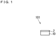
- FIG. 1 is a cross-sectional view illustrating a configuration of a semiconductor element 101 according to an Embodiment 1.
- the semiconductor element 101 includes a circuit element 2 and a transfer substrate 10.
- the transfer substrate 10 is joined to a lower surface of the circuit element 2.
- the circuit element 2 is a high electron mobility transistor (HEMT) having gallium nitride (GaN) as a semiconductor layer, but may be another circuit element such as a metal-oxide-semiconductor field-effect transistor (MOSFET) or an insulated gate bipolar transistor (IGBT).
- a thickness of the circuit element 2 is 10 ⁇ m, for example.
- the transfer substrate 10 is a substrate having high thermal conductivity, and is a diamond substrate, for example.
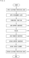
- FIG. 2 is a flow chart illustrating a method of manufacturing the semiconductor element 101. The method of manufacturing the semiconductor element 101 is described in accordance with a flow chart as shown in FIG. 2 .
- the circuit element substrate 7 includes a semiconductor substrate 1 and a circuit element 2 formed on the semiconductor substrate 1.
- the semiconductor substrate 1 is an Si wafer or an silicon carbide (SiC) wafer, for example.
- the circuit element 2 includes a hollow bridge electrode connecting an electrode and an electrode, and although not illustrated in FIG. 3 , there is a level difference caused by an electrode in an upper surface of the circuit element 2.
- a protection layer needs to be formed on the circuit element 2 to prevent breakage of the electrode in a subsequent polishing process.
- an electrode protection layer 3 is applied and formed on the circuit element 2 (Step S1).
- the electrode protection layer 3 has an effect of protecting the electrode of the circuit element 2 in the subsequent polishing process, and also has an effect of flattening unevenness of the electrode, thereby increasing joint strength of joining the electrode protection layer 3 to the support substrate.
- Selected for a material of the electrode protection layer 3 is an adhesive agent made up of an organic solvent and thermoset resin or photo-curable resin or a photoresist material which can be removed by a chemical treatment or oxide ashing in a final process.
- the electrode protection layer 3 is acrylic resin, olefin resin, phenol resin, polypropylene resin, or polyethylene resin, for example.
- Effective for the electrode protection layer 3 is a material having substrate strength achieved by the circuit element substrate 7 and the support substrate integrated with each other and having a high degree of hardness preventing detachment or a crack, for example, in the polishing process, and from this viewpoint, a material having high film strength such as acrylic resin or epoxy resin is preferable.
- the electrode protection layer 3 Used for application of the electrode protection layer 3 is a spin-coating method of dropping an adhesive agent to a main surface of the circuit element substrate 7 on which the circuit element 2 is formed and rotating the circuit element substrate 7 at a high speed, for example.
- the other application method such as a printing method or a spray method may be used.
- the electrode protection layer 3 is formed to cover the circuit element 2 at a thickness of 5 ⁇ m to 8 ⁇ m. After the electrode protection layer 3 is applied on the circuit element 2, the electrode protection layer 3 is hardened.
- thermoset resin used for the material of the electrode protection layer 3
- the electrode protection layer 3 is heated to have a temperature of 90 °C to 120 °C by a hot plate, for example, thus a solvent component thereof evaporates and the electrode protection layer 3 is hardened.
- photo-curable resin used for the material of the electrode protection layer 3
- the circuit element substrate 7 is irradiated with light, thus the electrode protection layer 3 is hardened.
- a detachment layer 5 is formed on an adhesive surface of a transparent substrate 4 to prepare a support substrate 8 (Step S2). That is to say, the support substrate 8 includes the transparent substrate 4 and the detachment layer 5 formed on the transparent substrate 4.
- the transparent substrate 4 includes light transparency, and is made of alkali-free grass or sapphire glass.
- the support substrate 8 is detached from the circuit element substrate 7 in the subsequent process, it takes time when a method such as etching, polishing, or dipping in a detachment solution is applied.
- the detachment layer 5 made up of a photodecomposition material decomposed when absorbing light such as laser or infrared light is formed on the transparent substrate 4.
- a paste made up of resin including a carbon material absorbing light, generating heat, and thermally decomposed and an organic solvent is applied to the transparent substrate 4 by a spin-coating method, and heat is applied to the paste to dry it, thus the detachment layer 5 is formed.
- a carbon film having a thickness of 1 ⁇ m to 2 ⁇ m as the detachment layer 5 may be formed on the transparent substrate 4 by a CVD sputtering device. When the carbon film is used for the detachment layer 5, the support substrate 8 can be firmly bonded to the circuit element substrate 7.
- Mirror finishing is preferably performed on a surface of the detachment layer 5 by lap polishing.
- An arithmetic average roughness of the surface of the detachment layer 5 is preferably smaller than 0.5 nm, and is more preferably smaller than 0.2 nm. When the arithmetic average roughness of the surface of the detachment layer 5 is smaller than 0.5 nm, a portion which is not bonded to the circuit element substrate 7 in the subsequent process can be reduced, and bonding strength between the detachment layer 5 and the circuit element substrate 7 is increased.
- the circuit element substrate 7 and the support substrate 8 are set in a vacuum chamber 9, and the vacuum chamber 9 is exhausted to an extremely-high vacuum 10 -6 Pa.
- a metal thin film 6 is formed to have a thickness of several nm to several tens of nm on the electrode protection layer 3 of the circuit element substrate 7 and the detachment layer 5 of the support substrate 8 by a sputtering method or an evaporation method, for example (Step S3).
- FIG. 6 illustrates sputtering atoms emitted from a sputtering target 12 on the electrode protection layer 3.
- Aluminum, copper, silicon, titanium, gold, silver, iron, or chrome, for example, is used for a material of the metal thin film 6.
- the metal thin films 6 are attached to each other in the vacuum chamber 9 to join the circuit element substrate 7 and the support substrate 8 (Step S4).
- the formation of the metal thin film 6 (Step S3) and the joining of the circuit element substrate 7 and the support substrate 8 (Step S4) are continuously performed in the same vacuum chamber 9.
- the circuit element substrate 7 and the support substrate 8 need to be irradiated with an ion beam ora neutral atomic beam in vacuum again and cleaned to attach the circuit element substrate 7 and the support substrate 8.
- applied in the present embodiment is an atomic diffusion joining method of forming the metal thin film 6 on the circuit element substrate 7 and the support substrate 8 in vacuum and subsequently attaching the metal thin films 6 to each other in vacuum, thus the surface activation needs not be performed by atomic beam, for example.
- Step S3 and Step S4 a time for the joint process (Step S3 and Step S4) can be reduced to ten minutes to fifteen minutes. Accordingly, when a cassette capable of setting a plurality of wafers at one time and a load lock chamber as a spare exhaustion room is provided in the vacuum chamber 9, a time for the treatment can be reduced compared with a process of attaching the substrate using a general adhesive agent.
- a thickness of the resin film is large, that is several hundred ⁇ m to several mm, and a degree of elasticity of the resin film is small.
- substrate strength is low after bonding, and such a configuration causes a problem that a crack occurs in a peripheral portion of the circuit element substrate 7 at a time of polishing and thinning the circuit element substrate 7 or the circuit element substrate 7 is detached from the support substrate 8.
- the thickness of the bonding layer can be extremely thinned to be approximately 0.2 nm to 20 nm, that is equal to a size of one atom.
- achieved is direct bonding in which atoms in the two substrates joined to each other are mutually diffused, thus bonding force is large, and mechanical strength of the joint substrate is increased.
- the joint is performed at a normal temperature, thus the substrate is not thermally expanded by heat, thereby not being deflected.
- a material of the substrate to be joined is not limited.
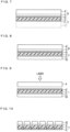
- Step S5 a surface of the joint substrate, which is made up of the circuit element substrate 7 and the support substrate 8, on a side of the circuit element substrate 7 is polished, and the semiconductor substrate 1 is removed.
- the semiconductor substrate 1 is removed to increase heat radiation efficiency of the circuit element 2, and obtain lower power consumption and high output.
- the semiconductor substrate 1 having a thickness of 500 ⁇ m is polished to have a thickness of 20 ⁇ m firstly.
- Mechanical polishing, chemical polishing, or chemical mechanical polishing, for example, is applied to a polishing method.
- the remaining semiconductor substrate 1 having a thickness of 20 ⁇ m is removed by dry etching such as reactive ion etching (RIE). Accordingly, the semiconductor substrate 1 is completely removed, and the lower surface of the circuit element 2 is exposed.
- RIE reactive ion etching
- an arithmetic average roughness Ra of the lower surface of the circuit element 2 is preferably equal to or smaller than 0.5 nm.
- the circuit element substrate 7 including the circuit element 2 decreases.
- the circuit element 2 is deformed by influence of stress of a remaining film, or a crack or detachment occurs in a peripheral portion of the circuit element 2 due to unevenness of polishing.
- the semiconductor substrate 1 is polished while the circuit element substrate 7 is firmly bonded to the support substrate 8, thus even when the semiconductor substrate 1 is removed, strength of the circuit element substrate 7 is maintained. Accordingly, a defect such as deformation, a crack, or detachment of the circuit element 2 is suppressed.
- Step S6 the lower surface of the circuit element 2 is joined to the transfer substrate 10 as illustrated in FIG. 8 (Step S6).
- a diamond substrate excellent in thermal conductivity, for example, is used for the transfer substrate 10.
- the transfer substrate 10 has a thickness of 100 ⁇ m, and an arithmetic average roughness of a joint surface is equal to or smaller than 0.5 nm by precision polishing.
- An atomic diffusion joining method which is the same as joining of the support substrate 8 described above is applied for joining of the transfer substrate 10.
- a thermal expansion coefficient of diamond constituting the transfer substrate 10 is 2.3 ⁇ 10 -6 /K, and is significantly different from a thermal expansion coefficient of gallium nitride constituting the circuit element 2, that is 5.5 ⁇ 10 -6 /K. Accordingly, it is difficult to thermally join the transfer substrate 10 to the circuit element 2. In the meanwhile, when the circuit element 2 and the transfer substrate 10 are directly joined by an extremely thin metal film having a thickness of several nm, thus a high heat radiation effect with small thermal resistance at a joint interface is obtained.
- the circuit element 2 and the transfer substrate 10 may be joined using a surface activating method of irradiating the joint surface with neutral atomic beam to remove a natural oxide film or an organic substance, and then attaching the joint surface.
- the joint surface between the circuit element 2 and the transfer substrate 10 is set to have an arithmetic average roughness of 0.5 nm or less by surface polishing.
- the support substrate 8 is detached from the circuit element substrate 7 as illustrated in FIG. 9 (Step S7).
- laser is emitted from an upper surface of the transparent substrate 4 to heat and decompose the detachment layer 5, thereby detaching the support substrate 8.
- the number of processes is reduced, a time for treatment is short, and the transparent substrate 4 can be reused compared with a method of removing the support substrate 8 by polishing or etching, thus productivity can be improved, and a manufacturing cost can be reduced.
- Step S8 dicing is performed as illustrated in FIG. 10 and FIG. 11 to divide the joint substrate made up of the transfer substrate 10 and the circuit element substrate 7 into a plurality of chips.
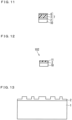
- FIG. 11 illustrates one chip after the division. A large number of elements are formed in the circuit element 2, and each element is divided in the present step.
- Laser dicing or plasma dicing can be applied to a dicing method.
- a crack, detachment, or a chip for example, conventionally occurs in the circuit element substrate 7 in the dicing process due to reduction in strength in accordance with thinning thereof.
- strength is increased by directly joining the circuit element substrate 7 to the support substrate 8, thus the defect described above is suppressed.
- Step S9 the metal thin film 6 and the electrode protection layer 3 are detached from the divided chips.
- the circuit element substrate 7 is dipped in alkali or acid detachment solution or organic solvent, for example, to dissolve the metal thin film 6 and the electrode protection layer 3 for removal.
- the circuit element substrate 7 is dried.
- the metal thin film 6 is removed by an acid detachment solution, and the electrode protection layer 3 is removed by oxide ashing. In this manner, the semiconductor element 101 illustrated in FIG. 1 is completed.
- the circuit element substrate 7 including the semiconductor substrate 1 and the circuit element 2 on the semiconductor substrate 1 are prepared, the electrode protection layer 3 is formed on the circuit element 2, the support substrate 8 is prepared, the metal thin film 6 is formed on the electrode protection layer 3 of the circuit element substrate 7 and the support substrate 8 in vacuum, the metal thin films 6 of the circuit element substrate 7 and the support substrate 8 are attached by an atomic diffusion joining method to join the circuit element substrate 7 and the support substrate 8, the semiconductor substrate 1 is removed by polishing to expose the circuit element 2, the transfer substrate 10 is joined to the exposed surface of the circuit element 2, and the support substrate 8 is detached from the circuit element 2 after joining the transfer substrate 10.
- the metal thin films 6 of the circuit element substrate 7 and the support substrate 8 are firmly bonded by the atomic diffusion joining method, thus mechanical strength of the joint substrate made up of the circuit element substrate 7 and the support substrate 8 joined to each other is increased. Accordingly, even when the semiconductor substrate 1 is polished to thin the semiconductor element, a defect such as a crack, detachment, or breakage hardly occurs in the circuit element 2, and a defect rate can be reduced.
- FIG. 12 is a cross-sectional view of a semiconductor element 102 according to an Embodiment 2.
- the semiconductor element 102 includes the circuit element 2, an inorganic insulating film 11 formed on the upper surface of the circuit element 2, and the transfer substrate 10 formed on the lower surface of the circuit element 2.
- the circuit element 2 and the transfer substrate 10 are as described in the Embodiment 1.
- the inorganic insulating film 11 is an electrode protection layer. Although resin is used for the electrode protection layer 3 in the Embodiment 1, an inorganic insulating film having high thermal conductivity is used as the electrode protection layer in the Embodiment 2, thus is referred to as the inorganic insulating film 11.
- the inorganic insulating film When the inorganic insulating film is used for the electrode protection layer, strength of the joint substrate made up of the circuit element substrate 7 and the support substrate 8 is increased, and a crack or detachment after polishing the semiconductor substrate 1 can be suppressed. However, it is difficult to remove the electrode protection layer in a final process, and the circuit element 2 after removal is significantly damaged.
- the inorganic insulating film 11 is not removed but is used as a heat radiation material on a side of the upper surface of the circuit element 2 in the semiconductor element 102, thus a heat radiation property of the semiconductor element 102 is increased, and a process of removing the inorganic insulating film 11 is omitted.
- the inorganic insulating film 11 is used as the heat radiation material, thus the inorganic insulating film 11 is an inorganic insulating film having high thermal conductivity.
- FIG. 13 to FIG. 15 are cross-sectional views each illustrating the inorganic insulating film 11 as the electrode protection layer formed on the circuit element 2 of the circuit element substrate 7.
- FIG. 13 illustrates the semiconductor substrate 1 and the circuit element substrate 7 including the circuit element 2 on the semiconductor substrate 1.
- the circuit element 2 includes a hollow bridge electrode connecting an electrode and an electrode, thus a level difference is formed in the upper surface of the circuit element 2 as illustrated in FIG. 13 .
- a height of the level difference is approximately several ⁇ m.
- the circuit element substrate 7 is disposed in a layer formation device such as a CVD plasma device, and as illustrated in FIG. 14 , the inorganic insulating film 11 having high thermal conductivity is formed on the circuit element 2 to have a thickness equal to or larger than a height of an electrode of the circuit element 2.
- Diamond, aluminum nitride, silicon nitride, or beryllium oxide, for example, can be used as a material of the inorganic insulating film 11.
- the inorganic insulating film 11 having high thermal conductivity is used as the electrode protection layer, thus the electrode protection layer can be used as a heat sink on a side of the upper surface of the circuit element 2, and the process of removing the electrode protection layer is unnecessary. Thus, reduction in time for the process and improvement of a device performance can be achieved.
- Silicon oxide for example, which is the insulating film but has low thermal conductivity needs to be removed in a final process by reason that it has a low heat radiation property and has a negative influence on the device performance.
- the circuit element 2 is damaged in the removal process, thus it is difficult to use a material such as silicon oxide as the material of the inorganic insulating film 11.
- the electrode protection layer 3 according to the Embodiment 1 is resin, thus when a spin-coating method is applied, the resin flows and the upper surface of the electrode protection layer 3 is flatly formed.
- the inorganic insulating film 11 is formed by a CVD method, for example, a level difference occurs in the upper surface of the inorganic insulating film 11 as illustrated in FIG. 14 .
- the upper surface of the inorganic insulating film 11 needs to be flattened to bond the whole upper surface of the inorganic insulating film 11 to the support substrate 8.
- a high portion of the inorganic insulating film 11 is flattened to have the same height as the electrode of the circuit element 2 by a polishing method.
- An arithmetic average roughness of the upper surface of the inorganic insulating film 11 at this time is equal to or smaller than 1.0 nm.
- Step S3 formation of the metal thin film 6 (Step S3), joining of the circuit element substrate 7 (Step S4) and the support substrate 8 (Step S5), polishing of the semiconductor substrate 1 (Step S6), joining of the transfer substrate 10 (Step S7), detachment of the support substrate 8 (Step S8), and division of the circuit element 2 (Step S9).
- the metal thin film 6 is removed from the upper surface of the inorganic insulating film 11, and the semiconductor element 102 illustrated in FIG. 12 is completed.
- the inorganic insulating film 11 remains on the upper surface of the circuit element 2, and functions as a heat sink.
- the electrode protection layer formed on the upper surface of the circuit element 2 is the inorganic insulating film 11 made up of an inorganic insulating material. Accordingly, strength of the joint substrate made up of the circuit element substrate 7 and the support substrate 8 is increased compared with a case of using resin for the electrode protection layer, and a crack or detachment after polishing the semiconductor substrate 1 can be suppressed.
- the inorganic insulating film 11 is an inorganic insulating film having high thermal conductivity
- the inorganic insulating film 11 can be used not only as the electrode protection layer but also as a heat radiation material on the side of the upper surface of the circuit element 2. Accordingly, the heat radiation property of the semiconductor element 102 can be increased, and the process of removing the electrode protection layer can be omitted.
Landscapes
- Mechanical Treatment Of Semiconductor (AREA)
Abstract
Description
- The present invention relates to a method of manufacturing a semiconductor element.
- Conventionally required is reduction in a thickness of a semiconductor element (also referred to as thinning) to pack the semiconductor element at a high density and downsize a semiconductor module or to join a heat radiation substrate to the semiconductor element and increase performance. Thinning of the semiconductor element is performed by the following processes.
- Firstly, a circuit element surface of the semiconductor element is bonded to a support substrate, and a surface on a side opposite to the circuit element surface is mechanically and chemically polished. Next, the support substrate is detached from the semiconductor element. A crack or damage on the thinned semiconductor element needs to be prevented in these processes.
-
Patent Document 1 discloses a method of bonding a semiconductor substrate having a thickness of 1130 µm to a support substrate by an electron wax, polishing a back surface of the semiconductor substrate, joining a transfer substrate to the back surface of the semiconductor substrate, and heating them to detach the support substrate. -
Patent Document 2 discloses a method of removing a substrate not by polishing but etching. Particularly, an organic insulating film is applied on a semiconductor layer on an Si substrate except for an end portion of a wafer made up of the Si substrate and the semiconductor layer. Next, an inorganic insulating film is formed to cover the organic insulating film. Subsequently, surfaces of the wafer and a support substrate are activated in vacuum, and the wafer is attached to the support substrate. Subsequently, an Si substrate is removed by etching. - Patent Document 3 describes a method of manufacturing a semiconductor element having a chip-on-chip structure. In the manufacturing method in Patent Document 3, a semiconductor wafer includes an Si substrate and an element layer on the Si substrate. A through electrode extending to both the Si substrate and the element layer is formed.
- A metal layer of the semiconductor wafer is attached to a metal layer of a support substrate after an insulating film and a metal film are sequentially formed on the element layer. A back surface of the wafer is polished until the through electrode is exposed from the back surface, the support substrate is removed by polishing and etching.
-
- Patent Document 1:
Japanese Patent Application Laid-Open JP 2005 129 825 A - Patent Document 2:
Japanese Patent Application Laid-Open JP 2012 28 477 A - Patent Document 3:
Japanese Patent Application Laid-Open JP 2007 324 406 A - In the conventional methods described in
Patent Documents 1 to 3, a substrate including a circuit element can be thinned to some degree of thickness. However, when the substrate on the back surface is wholly removed to thin the circuit element to 10 µm or less, the substrate which has supported the circuit element does not exist, thus there is a problem that strength of the semiconductor element decreases, a defect such as a crack, breakage, or film detachment occurs in the semiconductor element at a time of polishing, dicing, or detaching the support substrate, and a defect rate increases. - The present invention therefore has been made to solve the above problems, and it is an object to provide a method of manufacturing a thin semiconductor element having a low defect rate.
- A method of manufacturing a semiconductor element according to the present invention includes: preparing a circuit element substrate including a semiconductor substrate and a circuit element on the semiconductor substrate; forming an electrode protection layer on the circuit element; preparing a support substrate; forming a metal thin film on the electrode protection layer of the circuit element substrate and the support substrate in vacuum; attaching the metal thin film of the circuit element substrate and the metal thin film of the support substrate by an atomic diffusion joining method, thereby joining the circuit element substrate and the support substrate; removing the semiconductor substrate by polishing to expose the circuit element; joining a transfer substrate to an exposed surface of the circuit element; and detaching the support substrate from the circuit element after joining the transfer substrate.
- According to the method of manufacturing the semiconductor element according to the present invention, a thin semiconductor element in which a crack, detachment, or breakage hardly occurs in a circuit element even when a semiconductor substrate is removed by polishing and having a low defect rate can be manufactured. These and other objects, features, aspects and advantages of the present invention will become more apparent from the following detailed description when taken in conjunction with the accompanying drawings.
-
- FIG. 1
- A cross-sectional view illustrating a semiconductor element according to an
Embodiment 1. - FIG. 2
- A flow chart illustrating a method of manufacturing the semiconductor element according to the
Embodiment 1. - FIG. 3
- A cross-sectional view illustrating the method of manufacturing the semiconductor element according to the
Embodiment 1. - FIG. 4
- A cross-sectional view illustrating the method of manufacturing the semiconductor element according to the
Embodiment 1. - FIG. 5
- A cross-sectional view illustrating the method of manufacturing the semiconductor element according to the
Embodiment 1. - FIG. 6
- A cross-sectional view illustrating the method of manufacturing the semiconductor element according to the
Embodiment 1. - FIG. 7
- A cross-sectional view illustrating the method of manufacturing the semiconductor element according to the
Embodiment 1. - FIG. 8
- A cross-sectional view illustrating the method of manufacturing the semiconductor element according to the
Embodiment 1. - FIG. 9
- A cross-sectional view illustrating the method of manufacturing the semiconductor element according to the
Embodiment 1. - FIG. 10
- A cross-sectional view illustrating the method of manufacturing the semiconductor element according to the
Embodiment 1. - FIG. 11
- A cross-sectional view illustrating the method of manufacturing the semiconductor element according to the
Embodiment 1. - FIG. 12
- A cross-sectional view illustrating a semiconductor element according to an
Embodiment 2. - FIG. 13
- A cross-sectional view illustrating a method of manufacturing the semiconductor element according to the
Embodiment 2. - FIG. 14
- A cross-sectional view illustrating the method of manufacturing the semiconductor element according to the
Embodiment 2. - FIG. 15
- A cross-sectional view illustrating the method of manufacturing the semiconductor element according to the
Embodiment 2. -
FIG. 1 is a cross-sectional view illustrating a configuration of asemiconductor element 101 according to anEmbodiment 1. Thesemiconductor element 101 includes acircuit element 2 and atransfer substrate 10. Thetransfer substrate 10 is joined to a lower surface of thecircuit element 2. In the description hereinafter, thecircuit element 2 is a high electron mobility transistor (HEMT) having gallium nitride (GaN) as a semiconductor layer, but may be another circuit element such as a metal-oxide-semiconductor field-effect transistor (MOSFET) or an insulated gate bipolar transistor (IGBT). A thickness of thecircuit element 2 is 10 µm, for example. Thetransfer substrate 10 is a substrate having high thermal conductivity, and is a diamond substrate, for example. -
FIG. 2 is a flow chart illustrating a method of manufacturing thesemiconductor element 101. The method of manufacturing thesemiconductor element 101 is described in accordance with a flow chart as shown inFIG. 2 . - Firstly, a
circuit element substrate 7 is prepared as illustrated inFIG. 3 . Thecircuit element substrate 7 includes asemiconductor substrate 1 and acircuit element 2 formed on thesemiconductor substrate 1. Thesemiconductor substrate 1 is an Si wafer or an silicon carbide (SiC) wafer, for example. - The
circuit element 2 includes a hollow bridge electrode connecting an electrode and an electrode, and although not illustrated inFIG. 3 , there is a level difference caused by an electrode in an upper surface of thecircuit element 2. A protection layer needs to be formed on thecircuit element 2 to prevent breakage of the electrode in a subsequent polishing process. - Thus, as illustrated in
FIG. 4 , an electrode protection layer 3 is applied and formed on the circuit element 2 (Step S1). The electrode protection layer 3 has an effect of protecting the electrode of thecircuit element 2 in the subsequent polishing process, and also has an effect of flattening unevenness of the electrode, thereby increasing joint strength of joining the electrode protection layer 3 to the support substrate. - Selected for a material of the electrode protection layer 3 is an adhesive agent made up of an organic solvent and thermoset resin or photo-curable resin or a photoresist material which can be removed by a chemical treatment or oxide ashing in a final process.
- Generally used for the electrode protection layer 3 is acrylic resin, olefin resin, phenol resin, polypropylene resin, or polyethylene resin, for example. Effective for the electrode protection layer 3 is a material having substrate strength achieved by the
circuit element substrate 7 and the support substrate integrated with each other and having a high degree of hardness preventing detachment or a crack, for example, in the polishing process, and from this viewpoint, a material having high film strength such as acrylic resin or epoxy resin is preferable. - Used for application of the electrode protection layer 3 is a spin-coating method of dropping an adhesive agent to a main surface of the
circuit element substrate 7 on which thecircuit element 2 is formed and rotating thecircuit element substrate 7 at a high speed, for example. However, the other application method such as a printing method or a spray method may be used. The electrode protection layer 3 is formed to cover thecircuit element 2 at a thickness of 5 µm to 8 µm. After the electrode protection layer 3 is applied on thecircuit element 2, the electrode protection layer 3 is hardened. - In a case where thermoset resin is used for the material of the electrode protection layer 3, the electrode protection layer 3 is heated to have a temperature of 90 °C to 120 °C by a hot plate, for example, thus a solvent component thereof evaporates and the electrode protection layer 3 is hardened. In a case where photo-curable resin is used for the material of the electrode protection layer 3, the
circuit element substrate 7 is irradiated with light, thus the electrode protection layer 3 is hardened. - Next, as illustrated in
FIG. 5 , adetachment layer 5 is formed on an adhesive surface of atransparent substrate 4 to prepare a support substrate 8 (Step S2). That is to say, thesupport substrate 8 includes thetransparent substrate 4 and thedetachment layer 5 formed on thetransparent substrate 4. - The
transparent substrate 4 includes light transparency, and is made of alkali-free grass or sapphire glass. In a case where thesupport substrate 8 is detached from thecircuit element substrate 7 in the subsequent process, it takes time when a method such as etching, polishing, or dipping in a detachment solution is applied. Thus, in the present embodiment, thedetachment layer 5 made up of a photodecomposition material decomposed when absorbing light such as laser or infrared light is formed on thetransparent substrate 4. - For example, a paste made up of resin including a carbon material absorbing light, generating heat, and thermally decomposed and an organic solvent is applied to the
transparent substrate 4 by a spin-coating method, and heat is applied to the paste to dry it, thus thedetachment layer 5 is formed. A carbon film having a thickness of 1 µm to 2 µm as thedetachment layer 5 may be formed on thetransparent substrate 4 by a CVD sputtering device. When the carbon film is used for thedetachment layer 5, thesupport substrate 8 can be firmly bonded to thecircuit element substrate 7. - Mirror finishing is preferably performed on a surface of the
detachment layer 5 by lap polishing. An arithmetic average roughness of the surface of thedetachment layer 5 is preferably smaller than 0.5 nm, and is more preferably smaller than 0.2 nm. When the arithmetic average roughness of the surface of thedetachment layer 5 is smaller than 0.5 nm, a portion which is not bonded to thecircuit element substrate 7 in the subsequent process can be reduced, and bonding strength between thedetachment layer 5 and thecircuit element substrate 7 is increased. - Next, as illustrated in
FIG. 6 , thecircuit element substrate 7 and thesupport substrate 8 are set in avacuum chamber 9, and thevacuum chamber 9 is exhausted to an extremely-high vacuum 10-6 Pa. In this extremely-high vacuum state, a metalthin film 6 is formed to have a thickness of several nm to several tens of nm on the electrode protection layer 3 of thecircuit element substrate 7 and thedetachment layer 5 of thesupport substrate 8 by a sputtering method or an evaporation method, for example (Step S3).FIG. 6 illustrates sputtering atoms emitted from asputtering target 12 on the electrode protection layer 3. Aluminum, copper, silicon, titanium, gold, silver, iron, or chrome, for example, is used for a material of the metalthin film 6. - Then, the metal
thin films 6 are attached to each other in thevacuum chamber 9 to join thecircuit element substrate 7 and the support substrate 8 (Step S4). The formation of the metal thin film 6 (Step S3) and the joining of thecircuit element substrate 7 and the support substrate 8 (Step S4) are continuously performed in thesame vacuum chamber 9. - When the
circuit element substrate 7 and thesupport substrate 8 are taken out to the air after the formation of the metalthin film 6, moisture, a natural oxide film, or an organic substance adheres to surfaces of the metalthin films 6, and the metalthin films 6 are not joined to each other. - Thus, the
circuit element substrate 7 and thesupport substrate 8 need to be irradiated with an ion beam ora neutral atomic beam in vacuum again and cleaned to attach thecircuit element substrate 7 and thesupport substrate 8. In the meantime, applied in the present embodiment is an atomic diffusion joining method of forming the metalthin film 6 on thecircuit element substrate 7 and thesupport substrate 8 in vacuum and subsequently attaching the metalthin films 6 to each other in vacuum, thus the surface activation needs not be performed by atomic beam, for example. - Thus, there is no loss in the process, and a time for the joint process (Step S3 and Step S4) can be reduced to ten minutes to fifteen minutes. Accordingly, when a cassette capable of setting a plurality of wafers at one time and a load lock chamber as a spare exhaustion room is provided in the
vacuum chamber 9, a time for the treatment can be reduced compared with a process of attaching the substrate using a general adhesive agent. - In a conventional technique using a wax or thermoset or photo-curable resin for bonding the
circuit element substrate 7 and thesupport substrate 8, a thickness of the resin film is large, that is several hundred µm to several mm, and a degree of elasticity of the resin film is small. Thus, substrate strength is low after bonding, and such a configuration causes a problem that a crack occurs in a peripheral portion of thecircuit element substrate 7 at a time of polishing and thinning thecircuit element substrate 7 or thecircuit element substrate 7 is detached from thesupport substrate 8. - However, according to the atomic diffusion joining method of the present embodiment, the thickness of the bonding layer can be extremely thinned to be approximately 0.2 nm to 20 nm, that is equal to a size of one atom. In the atomic diffusion joining method, achieved is direct bonding in which atoms in the two substrates joined to each other are mutually diffused, thus bonding force is large, and mechanical strength of the joint substrate is increased.
- Thus, a defect such as a crack, detachment, or breakage at a time of polishing or dicing is reduced. According to the atomic diffusion joining method, the joint is performed at a normal temperature, thus the substrate is not thermally expanded by heat, thereby not being deflected. Thus, a material of the substrate to be joined is not limited.
- Next, as illustrated in
FIG. 7 , a surface of the joint substrate, which is made up of thecircuit element substrate 7 and thesupport substrate 8, on a side of thecircuit element substrate 7 is polished, and thesemiconductor substrate 1 is removed (Step S5). Thesemiconductor substrate 1 is removed to increase heat radiation efficiency of thecircuit element 2, and obtain lower power consumption and high output. - In the present step, the
semiconductor substrate 1 having a thickness of 500 µm is polished to have a thickness of 20 µm firstly. Mechanical polishing, chemical polishing, or chemical mechanical polishing, for example, is applied to a polishing method. Next, the remainingsemiconductor substrate 1 having a thickness of 20 µm is removed by dry etching such as reactive ion etching (RIE). Accordingly, thesemiconductor substrate 1 is completely removed, and the lower surface of thecircuit element 2 is exposed. - Subsequently, chemical mechanical polishing is performed, and flatness of the lower surface of the
circuit element 2 is obtained. In consideration of joining to thetransfer substrate 10 which will be performed afterward, an arithmetic average roughness Ra of the lower surface of thecircuit element 2 is preferably equal to or smaller than 0.5 nm. - As the
semiconductor substrate 1 is gradually thinned by polishing, strength of thecircuit element substrate 7 including thecircuit element 2 decreases. Thus, thecircuit element 2 is deformed by influence of stress of a remaining film, or a crack or detachment occurs in a peripheral portion of thecircuit element 2 due to unevenness of polishing. - However, in the present embodiment, the
semiconductor substrate 1 is polished while thecircuit element substrate 7 is firmly bonded to thesupport substrate 8, thus even when thesemiconductor substrate 1 is removed, strength of thecircuit element substrate 7 is maintained. Accordingly, a defect such as deformation, a crack, or detachment of thecircuit element 2 is suppressed. - Next, the lower surface of the
circuit element 2 is joined to thetransfer substrate 10 as illustrated inFIG. 8 (Step S6). A diamond substrate excellent in thermal conductivity, for example, is used for thetransfer substrate 10. Thetransfer substrate 10 has a thickness of 100 µm, and an arithmetic average roughness of a joint surface is equal to or smaller than 0.5 nm by precision polishing. An atomic diffusion joining method which is the same as joining of thesupport substrate 8 described above is applied for joining of thetransfer substrate 10. - A thermal expansion coefficient of diamond constituting the
transfer substrate 10 is 2.3 × 10⁻⁶/K, and is significantly different from a thermal expansion coefficient of gallium nitride constituting thecircuit element 2, that is 5.5 × 10⁻⁶/K. Accordingly, it is difficult to thermally join thetransfer substrate 10 to thecircuit element 2. In the meanwhile, when thecircuit element 2 and thetransfer substrate 10 are directly joined by an extremely thin metal film having a thickness of several nm, thus a high heat radiation effect with small thermal resistance at a joint interface is obtained. - Alternatively, the
circuit element 2 and thetransfer substrate 10 may be joined using a surface activating method of irradiating the joint surface with neutral atomic beam to remove a natural oxide film or an organic substance, and then attaching the joint surface. In this case, the joint surface between thecircuit element 2 and thetransfer substrate 10 is set to have an arithmetic average roughness of 0.5 nm or less by surface polishing. - Next, the
support substrate 8 is detached from thecircuit element substrate 7 as illustrated inFIG. 9 (Step S7). Particularly, laser is emitted from an upper surface of thetransparent substrate 4 to heat and decompose thedetachment layer 5, thereby detaching thesupport substrate 8. According to this method, the number of processes is reduced, a time for treatment is short, and thetransparent substrate 4 can be reused compared with a method of removing thesupport substrate 8 by polishing or etching, thus productivity can be improved, and a manufacturing cost can be reduced. - Next, dicing is performed as illustrated in
FIG. 10 andFIG. 11 to divide the joint substrate made up of thetransfer substrate 10 and thecircuit element substrate 7 into a plurality of chips (Step S8).FIG. 11 illustrates one chip after the division. A large number of elements are formed in thecircuit element 2, and each element is divided in the present step. - Laser dicing or plasma dicing, for example, can be applied to a dicing method. A crack, detachment, or a chip, for example, conventionally occurs in the
circuit element substrate 7 in the dicing process due to reduction in strength in accordance with thinning thereof. However, in the present embodiment, strength is increased by directly joining thecircuit element substrate 7 to thesupport substrate 8, thus the defect described above is suppressed. - Next, the metal
thin film 6 and the electrode protection layer 3 are detached from the divided chips (Step S9). In the present step, thecircuit element substrate 7 is dipped in alkali or acid detachment solution or organic solvent, for example, to dissolve the metalthin film 6 and the electrode protection layer 3 for removal. - Then, a remaining organic substance is cleansed, and the
circuit element substrate 7 is dried. Alternatively, it is also applicable that the metalthin film 6 is removed by an acid detachment solution, and the electrode protection layer 3 is removed by oxide ashing. In this manner, thesemiconductor element 101 illustrated inFIG. 1 is completed. - As described above, according to the method of manufacturing the semiconductor element of the
Embodiment 1, thecircuit element substrate 7 including thesemiconductor substrate 1 and thecircuit element 2 on thesemiconductor substrate 1 are prepared, the electrode protection layer 3 is formed on thecircuit element 2, thesupport substrate 8 is prepared, the metalthin film 6 is formed on the electrode protection layer 3 of thecircuit element substrate 7 and thesupport substrate 8 in vacuum, the metalthin films 6 of thecircuit element substrate 7 and thesupport substrate 8 are attached by an atomic diffusion joining method to join thecircuit element substrate 7 and thesupport substrate 8, thesemiconductor substrate 1 is removed by polishing to expose thecircuit element 2, thetransfer substrate 10 is joined to the exposed surface of thecircuit element 2, and thesupport substrate 8 is detached from thecircuit element 2 after joining thetransfer substrate 10. - The metal
thin films 6 of thecircuit element substrate 7 and thesupport substrate 8 are firmly bonded by the atomic diffusion joining method, thus mechanical strength of the joint substrate made up of thecircuit element substrate 7 and thesupport substrate 8 joined to each other is increased. Accordingly, even when thesemiconductor substrate 1 is polished to thin the semiconductor element, a defect such as a crack, detachment, or breakage hardly occurs in thecircuit element 2, and a defect rate can be reduced. -
FIG. 12 is a cross-sectional view of asemiconductor element 102 according to anEmbodiment 2. Thesemiconductor element 102 includes thecircuit element 2, an inorganic insulatingfilm 11 formed on the upper surface of thecircuit element 2, and thetransfer substrate 10 formed on the lower surface of thecircuit element 2. Thecircuit element 2 and thetransfer substrate 10 are as described in theEmbodiment 1. The inorganic insulatingfilm 11 is an electrode protection layer. Although resin is used for the electrode protection layer 3 in theEmbodiment 1, an inorganic insulating film having high thermal conductivity is used as the electrode protection layer in theEmbodiment 2, thus is referred to as the inorganic insulatingfilm 11. - When the inorganic insulating film is used for the electrode protection layer, strength of the joint substrate made up of the
circuit element substrate 7 and thesupport substrate 8 is increased, and a crack or detachment after polishing thesemiconductor substrate 1 can be suppressed. However, it is difficult to remove the electrode protection layer in a final process, and thecircuit element 2 after removal is significantly damaged. - The inorganic insulating
film 11 is not removed but is used as a heat radiation material on a side of the upper surface of thecircuit element 2 in thesemiconductor element 102, thus a heat radiation property of thesemiconductor element 102 is increased, and a process of removing the inorganic insulatingfilm 11 is omitted. As described above, the inorganic insulatingfilm 11 is used as the heat radiation material, thus the inorganic insulatingfilm 11 is an inorganic insulating film having high thermal conductivity. -
FIG. 13 to FIG. 15 are cross-sectional views each illustrating the inorganic insulatingfilm 11 as the electrode protection layer formed on thecircuit element 2 of thecircuit element substrate 7.FIG. 13 illustrates thesemiconductor substrate 1 and thecircuit element substrate 7 including thecircuit element 2 on thesemiconductor substrate 1. - The
circuit element 2 includes a hollow bridge electrode connecting an electrode and an electrode, thus a level difference is formed in the upper surface of thecircuit element 2 as illustrated inFIG. 13 . A height of the level difference is approximately several µm. - The
circuit element substrate 7 is disposed in a layer formation device such as a CVD plasma device, and as illustrated inFIG. 14 , the inorganic insulatingfilm 11 having high thermal conductivity is formed on thecircuit element 2 to have a thickness equal to or larger than a height of an electrode of thecircuit element 2. Diamond, aluminum nitride, silicon nitride, or beryllium oxide, for example, can be used as a material of the inorganic insulatingfilm 11. - The inorganic insulating
film 11 having high thermal conductivity is used as the electrode protection layer, thus the electrode protection layer can be used as a heat sink on a side of the upper surface of thecircuit element 2, and the process of removing the electrode protection layer is unnecessary. Thus, reduction in time for the process and improvement of a device performance can be achieved. - Silicon oxide, for example, which is the insulating film but has low thermal conductivity needs to be removed in a final process by reason that it has a low heat radiation property and has a negative influence on the device performance. The
circuit element 2 is damaged in the removal process, thus it is difficult to use a material such as silicon oxide as the material of the inorganic insulatingfilm 11. - The electrode protection layer 3 according to the
Embodiment 1 is resin, thus when a spin-coating method is applied, the resin flows and the upper surface of the electrode protection layer 3 is flatly formed. However, when the inorganic insulatingfilm 11 is formed by a CVD method, for example, a level difference occurs in the upper surface of the inorganic insulatingfilm 11 as illustrated inFIG. 14 . - In order to obtain high bonding strength between the
circuit element substrate 7 and thesupport substrate 8, the upper surface of the inorganic insulatingfilm 11 needs to be flattened to bond the whole upper surface of the inorganic insulatingfilm 11 to thesupport substrate 8. - Thus, as illustrated in
FIG. 15 , a high portion of the inorganic insulatingfilm 11 is flattened to have the same height as the electrode of thecircuit element 2 by a polishing method. An arithmetic average roughness of the upper surface of the inorganic insulatingfilm 11 at this time is equal to or smaller than 1.0 nm. - Next, after the upper surface of the inorganic insulating
film 11 is cleansed to remove a polishing residue, performed in the manner similar to theEmbodiment 1 are formation of the metal thin film 6 (Step S3), joining of the circuit element substrate 7 (Step S4) and the support substrate 8 (Step S5), polishing of the semiconductor substrate 1 (Step S6), joining of the transfer substrate 10 (Step S7), detachment of the support substrate 8 (Step S8), and division of the circuit element 2 (Step S9). - Then, the metal
thin film 6 is removed from the upper surface of the inorganic insulatingfilm 11, and thesemiconductor element 102 illustrated inFIG. 12 is completed. The inorganic insulatingfilm 11 remains on the upper surface of thecircuit element 2, and functions as a heat sink. - In the method of manufacturing the semiconductor element according to the
Embodiment 2, the electrode protection layer formed on the upper surface of thecircuit element 2 is the inorganic insulatingfilm 11 made up of an inorganic insulating material. Accordingly, strength of the joint substrate made up of thecircuit element substrate 7 and thesupport substrate 8 is increased compared with a case of using resin for the electrode protection layer, and a crack or detachment after polishing thesemiconductor substrate 1 can be suppressed. - When the inorganic insulating
film 11 is an inorganic insulating film having high thermal conductivity, the inorganic insulatingfilm 11 can be used not only as the electrode protection layer but also as a heat radiation material on the side of the upper surface of thecircuit element 2. Accordingly, the heat radiation property of thesemiconductor element 102 can be increased, and the process of removing the electrode protection layer can be omitted. - Each embodiment can be arbitrarily combined, or each embodiment can be appropriately varied or omitted. The foregoing description is in all aspects illustrative. It is therefore understood that numerous modification examples not illustrated can be devised.
-
- 1
- Semiconductor substrate
- 2
- circuit element
- 3
- electrode protection layer
- 4
- transparent substrate
- 5
- detachment layer
- 6
- metal thin film
- 7
- circuit element substrate
- 8
- support substrate
- 9
- vacuum chamber
- 10
- transfer substrate
- 11
- inorganic insulating film
- 12
- sputtering target
- 101
- semiconductor element
- 102
- semiconductor element.
Claims (8)
- A method of manufacturing a semiconductor element, comprising:preparing a circuit element substrate including a semiconductor substrate and a circuit element on the semiconductor substrate;forming an electrode protection layer on the circuit element;preparing a support substrate;forming a metal thin film on the electrode protection layer of the circuit element substrate and the support substrate in vacuum;attaching the metal thin film of the circuit element substrate and the metal thin film of the support substrate by an atomic diffusion joining method, thereby joining the circuit element substrate and the support substrate;removing the semiconductor substrate by polishing to expose the circuit element;joining a transfer substrate to an exposed surface of the circuit element; anddetaching the support substrate from the circuit element after joining the transfer substrate.
- The method of manufacturing the semiconductor element according to claim 1, wherein formation of the metal thin film and joining of the circuit element substrate and the support substrate are continuously performed in an identical vacuum chamber.
- The method of manufacturing the semiconductor element according to claim 1 or 2,wherein the support substrate includes a transparent substrate and a detachment layer made up of a photodecomposition material formed on the transparent substrate,wherein the metal thin film is formed on the detachment layer of the support substrate, andwherein the support substrate is detached by performing photodecomposition on the detachment layer.
- The method of manufacturing the semiconductor element according to claim 3,wherein the detachment layer is made up of a carbon film, andwherein the support substrate is detached by emitting laser from a lower surface of the transparent substrate, thereby heating and decomposing the detachment layer.
- The method of manufacturing the semiconductor element according to any one of claims 1 to 4,
wherein the electrode protection layer is made up of acrylic resin or epoxy resin. - The method of manufacturing the semiconductor element according to any one of claims 1 to 4,
wherein the electrode protection layer is made up of an inorganic insulating material. - The method of manufacturing the semiconductor element according to claim 6, wherein the inorganic insulating material is any one of diamond, aluminum nitride, silicon nitride, or beryllium oxide.
- The method of manufacturing the semiconductor element according to any one of claims 1 to 7,wherein the circuit element includes gallium nitride as a semiconductor layer, andwherein the transfer substrate is made of diamond.
Applications Claiming Priority (1)
| Application Number | Priority Date | Filing Date | Title |
|---|---|---|---|
| PCT/JP2020/016312 WO2021210047A1 (en) | 2020-04-13 | 2020-04-13 | Method for manufacturing semiconductor element |
Publications (3)
| Publication Number | Publication Date |
|---|---|
| EP4138116A1 true EP4138116A1 (en) | 2023-02-22 |
| EP4138116A4 EP4138116A4 (en) | 2023-07-19 |
| EP4138116B1 EP4138116B1 (en) | 2024-03-13 |
Family
ID=78084736
Family Applications (1)
| Application Number | Title | Priority Date | Filing Date |
|---|---|---|---|
| EP20931548.0A Active EP4138116B1 (en) | 2020-04-13 | 2020-04-13 | Method for manufacturing semiconductor element |
Country Status (6)
| Country | Link |
|---|---|
| US (1) | US12387934B2 (en) |
| EP (1) | EP4138116B1 (en) |
| JP (1) | JP7186921B2 (en) |
| KR (1) | KR102718211B1 (en) |
| CN (1) | CN115428127B (en) |
| WO (1) | WO2021210047A1 (en) |
Cited By (1)
| Publication number | Priority date | Publication date | Assignee | Title |
|---|---|---|---|---|
| US20220415696A1 (en) * | 2021-06-24 | 2022-12-29 | Taiwan Semiconductor Manufacturing Co., Ltd. | Debonding structures for wafer bonding |
Families Citing this family (1)
| Publication number | Priority date | Publication date | Assignee | Title |
|---|---|---|---|---|
| JP2025020566A (en) * | 2023-07-31 | 2025-02-13 | 株式会社東芝 | Semiconductor device manufacturing method |
Family Cites Families (15)
| Publication number | Priority date | Publication date | Assignee | Title |
|---|---|---|---|---|
| JPH1174230A (en) * | 1997-08-29 | 1999-03-16 | Nippon Telegr & Teleph Corp <Ntt> | Method for manufacturing thin film semiconductor device |
| JPH11261198A (en) * | 1998-03-11 | 1999-09-24 | Dainippon Printing Co Ltd | Method of manufacturing wiring substrate using transfer master, transfer master, and method of manufacturing transfer master |
| US6593213B2 (en) * | 2001-09-20 | 2003-07-15 | Heliovolt Corporation | Synthesis of layers, coatings or films using electrostatic fields |
| JP2004055593A (en) * | 2002-07-16 | 2004-02-19 | Hoya Corp | Wiring board and its manufacturing method |
| JP2005129825A (en) | 2003-10-27 | 2005-05-19 | Sumitomo Chemical Co Ltd | Method for manufacturing compound semiconductor substrate |
| JP2007188967A (en) * | 2006-01-11 | 2007-07-26 | Sony Corp | Substrate support, substrate processing method, and semiconductor device manufacturing method |
| JP5003023B2 (en) | 2006-06-01 | 2012-08-15 | ソニー株式会社 | Substrate processing method and semiconductor device manufacturing method |
| JP2012028477A (en) | 2010-07-22 | 2012-02-09 | Sumitomo Electric Ind Ltd | Method of manufacturing semiconductor device |
| US20140144593A1 (en) * | 2012-11-28 | 2014-05-29 | International Business Machiness Corporation | Wafer debonding using long-wavelength infrared radiation ablation |
| JP6299478B2 (en) * | 2013-06-26 | 2018-03-28 | 日亜化学工業株式会社 | Light emitting device and manufacturing method thereof |
| JP6210152B2 (en) * | 2014-04-10 | 2017-10-11 | 富士電機株式会社 | Semiconductor substrate processing method and semiconductor device manufacturing method using the processing method |
| WO2018216763A1 (en) | 2017-05-25 | 2018-11-29 | 株式会社新川 | Method for producing structure, and structure |
| KR102558905B1 (en) | 2017-07-14 | 2023-07-21 | 신에쓰 가가꾸 고교 가부시끼가이샤 | High thermal conductivity device substrate and manufacturing method thereof |
| JP7041338B2 (en) * | 2017-09-01 | 2022-03-24 | 日亜化学工業株式会社 | Manufacturing method of light emitting device |
| JP7002398B2 (en) * | 2018-04-13 | 2022-01-20 | 株式会社ディスコ | How to join optical components |
-
2020
- 2020-04-13 EP EP20931548.0A patent/EP4138116B1/en active Active
- 2020-04-13 JP JP2022514883A patent/JP7186921B2/en active Active
- 2020-04-13 WO PCT/JP2020/016312 patent/WO2021210047A1/en not_active Ceased
- 2020-04-13 US US17/912,053 patent/US12387934B2/en active Active
- 2020-04-13 KR KR1020227032511A patent/KR102718211B1/en active Active
- 2020-04-13 CN CN202080099340.8A patent/CN115428127B/en active Active
Cited By (2)
| Publication number | Priority date | Publication date | Assignee | Title |
|---|---|---|---|---|
| US20220415696A1 (en) * | 2021-06-24 | 2022-12-29 | Taiwan Semiconductor Manufacturing Co., Ltd. | Debonding structures for wafer bonding |
| US12347717B2 (en) * | 2021-06-24 | 2025-07-01 | Taiwan Semiconductor Manufacturing Company, Ltd. | Debonding structures for wafer bonding |
Also Published As
| Publication number | Publication date |
|---|---|
| US20230134255A1 (en) | 2023-05-04 |
| WO2021210047A1 (en) | 2021-10-21 |
| EP4138116B1 (en) | 2024-03-13 |
| US12387934B2 (en) | 2025-08-12 |
| KR102718211B1 (en) | 2024-10-15 |
| JP7186921B2 (en) | 2022-12-09 |
| CN115428127A (en) | 2022-12-02 |
| JPWO2021210047A1 (en) | 2021-10-21 |
| CN115428127B (en) | 2025-02-18 |
| KR20220143741A (en) | 2022-10-25 |
| EP4138116A4 (en) | 2023-07-19 |
Similar Documents
| Publication | Publication Date | Title |
|---|---|---|
| JP7256120B2 (en) | Semiconductor device manufacturing method and wafer bonding structure | |
| JP5599342B2 (en) | Manufacturing method of semiconductor device | |
| CN113454758B (en) | Method for manufacturing semiconductor element | |
| TW201826332A (en) | Method for transferring device layer to transfer substrate and high thermal conductivity substrate | |
| US20120045611A1 (en) | Composite Carrier Structure | |
| CN105960707B (en) | Loading and unloading device chip removes | |
| JP6035468B2 (en) | Semiconductor-on-diamond wafer handle and manufacturing method | |
| CN114496723A (en) | Method for manufacturing semiconductor device and hot plate | |
| EP4138116B1 (en) | Method for manufacturing semiconductor element | |
| CN111599753A (en) | A thin wafer heat sink and its manufacturing process | |
| TW202425081A (en) | Semiconductor device manufacturing method | |
| CN113841223B (en) | Method for manufacturing semiconductor substrate and method for manufacturing semiconductor device | |
| CN111710647A (en) | A process of double-sided electroplating thick copper film for opening holes | |
| US11302538B2 (en) | Semiconductor device manufacturing method | |
| WO2022210680A1 (en) | Power semiconductor and method for manufacturing same | |
| JP2005129653A (en) | Manufacturing method of semiconductor device | |
| US20260047374A1 (en) | Method for manufacturing semiconductor device | |
| TWI835575B (en) | Manufacturing method of semiconductor wafer | |
| US20090081880A1 (en) | Method for manufacturing semiconductor device | |
| JP7182105B2 (en) | Method for manufacturing group III nitride semiconductor device | |
| EP4290553A1 (en) | Method for manufacturing semiconductor substrate and method for manufacturing semiconductor device | |
| CN118315287A (en) | A method for manufacturing a chip |
Legal Events
| Date | Code | Title | Description |
|---|---|---|---|
| STAA | Information on the status of an ep patent application or granted ep patent |
Free format text: STATUS: THE INTERNATIONAL PUBLICATION HAS BEEN MADE |
|
| PUAI | Public reference made under article 153(3) epc to a published international application that has entered the european phase |
Free format text: ORIGINAL CODE: 0009012 |
|
| STAA | Information on the status of an ep patent application or granted ep patent |
Free format text: STATUS: REQUEST FOR EXAMINATION WAS MADE |
|
| 17P | Request for examination filed |
Effective date: 20221004 |
|
| AK | Designated contracting states |
Kind code of ref document: A1 Designated state(s): AL AT BE BG CH CY CZ DE DK EE ES FI FR GB GR HR HU IE IS IT LI LT LU LV MC MK MT NL NO PL PT RO RS SE SI SK SM TR |
|
| REG | Reference to a national code |
Ref country code: DE Ref legal event code: R079 Free format text: PREVIOUS MAIN CLASS: H01L0021304000 Ipc: H01L0021683000 Ref country code: DE Ref legal event code: R079 Ref document number: 602020027367 Country of ref document: DE Free format text: PREVIOUS MAIN CLASS: H01L0021304000 Ipc: H01L0021683000 |
|
| A4 | Supplementary search report drawn up and despatched |
Effective date: 20230615 |
|
| DAV | Request for validation of the european patent (deleted) | ||
| DAX | Request for extension of the european patent (deleted) | ||
| RIC1 | Information provided on ipc code assigned before grant |
Ipc: H01L 21/78 20060101ALI20230609BHEP Ipc: H01L 21/683 20060101AFI20230609BHEP |
|
| REG | Reference to a national code |
Ref country code: DE Ref legal event code: R079 Free format text: PREVIOUS MAIN CLASS: H01L0021683000 Ipc: H01L0021180000 Ref country code: DE Ref legal event code: R079 Ref document number: 602020027367 Country of ref document: DE Free format text: PREVIOUS MAIN CLASS: H01L0021683000 Ipc: H01L0021180000 |
|
| GRAP | Despatch of communication of intention to grant a patent |
Free format text: ORIGINAL CODE: EPIDOSNIGR1 |
|
| STAA | Information on the status of an ep patent application or granted ep patent |
Free format text: STATUS: GRANT OF PATENT IS INTENDED |
|
| RIC1 | Information provided on ipc code assigned before grant |
Ipc: H01L 21/78 20060101ALI20230925BHEP Ipc: H01L 21/683 20060101ALI20230925BHEP Ipc: H01L 21/18 20060101AFI20230925BHEP |
|
| INTG | Intention to grant announced |
Effective date: 20231031 |
|
| GRAS | Grant fee paid |
Free format text: ORIGINAL CODE: EPIDOSNIGR3 |
|
| GRAA | (expected) grant |
Free format text: ORIGINAL CODE: 0009210 |
|
| STAA | Information on the status of an ep patent application or granted ep patent |
Free format text: STATUS: THE PATENT HAS BEEN GRANTED |
|
| AK | Designated contracting states |
Kind code of ref document: B1 Designated state(s): AL AT BE BG CH CY CZ DE DK EE ES FI FR GB GR HR HU IE IS IT LI LT LU LV MC MK MT NL NO PL PT RO RS SE SI SK SM TR |
|
| REG | Reference to a national code |
Ref country code: GB Ref legal event code: FG4D |
|
| REG | Reference to a national code |
Ref country code: CH Ref legal event code: EP |
|
| REG | Reference to a national code |
Ref country code: DE Ref legal event code: R096 Ref document number: 602020027367 Country of ref document: DE |
|
| REG | Reference to a national code |
Ref country code: IE Ref legal event code: FG4D |
|
| PG25 | Lapsed in a contracting state [announced via postgrant information from national office to epo] |
Ref country code: LT Free format text: LAPSE BECAUSE OF FAILURE TO SUBMIT A TRANSLATION OF THE DESCRIPTION OR TO PAY THE FEE WITHIN THE PRESCRIBED TIME-LIMIT Effective date: 20240313 |
|
| REG | Reference to a national code |
Ref country code: LT Ref legal event code: MG9D |
|
| PG25 | Lapsed in a contracting state [announced via postgrant information from national office to epo] |
Ref country code: GR Free format text: LAPSE BECAUSE OF FAILURE TO SUBMIT A TRANSLATION OF THE DESCRIPTION OR TO PAY THE FEE WITHIN THE PRESCRIBED TIME-LIMIT Effective date: 20240614 |
|
| REG | Reference to a national code |
Ref country code: NL Ref legal event code: MP Effective date: 20240313 |
|
| PG25 | Lapsed in a contracting state [announced via postgrant information from national office to epo] |
Ref country code: HR Free format text: LAPSE BECAUSE OF FAILURE TO SUBMIT A TRANSLATION OF THE DESCRIPTION OR TO PAY THE FEE WITHIN THE PRESCRIBED TIME-LIMIT Effective date: 20240313 Ref country code: RS Free format text: LAPSE BECAUSE OF FAILURE TO SUBMIT A TRANSLATION OF THE DESCRIPTION OR TO PAY THE FEE WITHIN THE PRESCRIBED TIME-LIMIT Effective date: 20240613 |
|
| PG25 | Lapsed in a contracting state [announced via postgrant information from national office to epo] |
Ref country code: ES Free format text: LAPSE BECAUSE OF FAILURE TO SUBMIT A TRANSLATION OF THE DESCRIPTION OR TO PAY THE FEE WITHIN THE PRESCRIBED TIME-LIMIT Effective date: 20240313 |
|
| PG25 | Lapsed in a contracting state [announced via postgrant information from national office to epo] |
Ref country code: RS Free format text: LAPSE BECAUSE OF FAILURE TO SUBMIT A TRANSLATION OF THE DESCRIPTION OR TO PAY THE FEE WITHIN THE PRESCRIBED TIME-LIMIT Effective date: 20240613 Ref country code: NO Free format text: LAPSE BECAUSE OF FAILURE TO SUBMIT A TRANSLATION OF THE DESCRIPTION OR TO PAY THE FEE WITHIN THE PRESCRIBED TIME-LIMIT Effective date: 20240613 Ref country code: LT Free format text: LAPSE BECAUSE OF FAILURE TO SUBMIT A TRANSLATION OF THE DESCRIPTION OR TO PAY THE FEE WITHIN THE PRESCRIBED TIME-LIMIT Effective date: 20240313 Ref country code: HR Free format text: LAPSE BECAUSE OF FAILURE TO SUBMIT A TRANSLATION OF THE DESCRIPTION OR TO PAY THE FEE WITHIN THE PRESCRIBED TIME-LIMIT Effective date: 20240313 Ref country code: GR Free format text: LAPSE BECAUSE OF FAILURE TO SUBMIT A TRANSLATION OF THE DESCRIPTION OR TO PAY THE FEE WITHIN THE PRESCRIBED TIME-LIMIT Effective date: 20240614 Ref country code: FI Free format text: LAPSE BECAUSE OF FAILURE TO SUBMIT A TRANSLATION OF THE DESCRIPTION OR TO PAY THE FEE WITHIN THE PRESCRIBED TIME-LIMIT Effective date: 20240313 Ref country code: ES Free format text: LAPSE BECAUSE OF FAILURE TO SUBMIT A TRANSLATION OF THE DESCRIPTION OR TO PAY THE FEE WITHIN THE PRESCRIBED TIME-LIMIT Effective date: 20240313 Ref country code: BG Free format text: LAPSE BECAUSE OF FAILURE TO SUBMIT A TRANSLATION OF THE DESCRIPTION OR TO PAY THE FEE WITHIN THE PRESCRIBED TIME-LIMIT Effective date: 20240313 |
|
| REG | Reference to a national code |
Ref country code: AT Ref legal event code: MK05 Ref document number: 1666572 Country of ref document: AT Kind code of ref document: T Effective date: 20240313 |
|
| PG25 | Lapsed in a contracting state [announced via postgrant information from national office to epo] |
Ref country code: SE Free format text: LAPSE BECAUSE OF FAILURE TO SUBMIT A TRANSLATION OF THE DESCRIPTION OR TO PAY THE FEE WITHIN THE PRESCRIBED TIME-LIMIT Effective date: 20240313 Ref country code: LV Free format text: LAPSE BECAUSE OF FAILURE TO SUBMIT A TRANSLATION OF THE DESCRIPTION OR TO PAY THE FEE WITHIN THE PRESCRIBED TIME-LIMIT Effective date: 20240313 |
|
| PG25 | Lapsed in a contracting state [announced via postgrant information from national office to epo] |
Ref country code: NL Free format text: LAPSE BECAUSE OF FAILURE TO SUBMIT A TRANSLATION OF THE DESCRIPTION OR TO PAY THE FEE WITHIN THE PRESCRIBED TIME-LIMIT Effective date: 20240313 |
|
| PG25 | Lapsed in a contracting state [announced via postgrant information from national office to epo] |
Ref country code: NL Free format text: LAPSE BECAUSE OF FAILURE TO SUBMIT A TRANSLATION OF THE DESCRIPTION OR TO PAY THE FEE WITHIN THE PRESCRIBED TIME-LIMIT Effective date: 20240313 |
|
| PG25 | Lapsed in a contracting state [announced via postgrant information from national office to epo] |
Ref country code: IS Free format text: LAPSE BECAUSE OF FAILURE TO SUBMIT A TRANSLATION OF THE DESCRIPTION OR TO PAY THE FEE WITHIN THE PRESCRIBED TIME-LIMIT Effective date: 20240713 |
|
| PG25 | Lapsed in a contracting state [announced via postgrant information from national office to epo] |
Ref country code: PT Free format text: LAPSE BECAUSE OF FAILURE TO SUBMIT A TRANSLATION OF THE DESCRIPTION OR TO PAY THE FEE WITHIN THE PRESCRIBED TIME-LIMIT Effective date: 20240715 Ref country code: SM Free format text: LAPSE BECAUSE OF FAILURE TO SUBMIT A TRANSLATION OF THE DESCRIPTION OR TO PAY THE FEE WITHIN THE PRESCRIBED TIME-LIMIT Effective date: 20240313 |
|
| PG25 | Lapsed in a contracting state [announced via postgrant information from national office to epo] |
Ref country code: CZ Free format text: LAPSE BECAUSE OF FAILURE TO SUBMIT A TRANSLATION OF THE DESCRIPTION OR TO PAY THE FEE WITHIN THE PRESCRIBED TIME-LIMIT Effective date: 20240313 Ref country code: EE Free format text: LAPSE BECAUSE OF FAILURE TO SUBMIT A TRANSLATION OF THE DESCRIPTION OR TO PAY THE FEE WITHIN THE PRESCRIBED TIME-LIMIT Effective date: 20240313 |
|
| PG25 | Lapsed in a contracting state [announced via postgrant information from national office to epo] |
Ref country code: AT Free format text: LAPSE BECAUSE OF FAILURE TO SUBMIT A TRANSLATION OF THE DESCRIPTION OR TO PAY THE FEE WITHIN THE PRESCRIBED TIME-LIMIT Effective date: 20240313 |
|
| PG25 | Lapsed in a contracting state [announced via postgrant information from national office to epo] |
Ref country code: PL Free format text: LAPSE BECAUSE OF FAILURE TO SUBMIT A TRANSLATION OF THE DESCRIPTION OR TO PAY THE FEE WITHIN THE PRESCRIBED TIME-LIMIT Effective date: 20240313 |
|
| PG25 | Lapsed in a contracting state [announced via postgrant information from national office to epo] |
Ref country code: SK Free format text: LAPSE BECAUSE OF FAILURE TO SUBMIT A TRANSLATION OF THE DESCRIPTION OR TO PAY THE FEE WITHIN THE PRESCRIBED TIME-LIMIT Effective date: 20240313 |
|
| PG25 | Lapsed in a contracting state [announced via postgrant information from national office to epo] |
Ref country code: SM Free format text: LAPSE BECAUSE OF FAILURE TO SUBMIT A TRANSLATION OF THE DESCRIPTION OR TO PAY THE FEE WITHIN THE PRESCRIBED TIME-LIMIT Effective date: 20240313 Ref country code: SK Free format text: LAPSE BECAUSE OF FAILURE TO SUBMIT A TRANSLATION OF THE DESCRIPTION OR TO PAY THE FEE WITHIN THE PRESCRIBED TIME-LIMIT Effective date: 20240313 Ref country code: RO Free format text: LAPSE BECAUSE OF FAILURE TO SUBMIT A TRANSLATION OF THE DESCRIPTION OR TO PAY THE FEE WITHIN THE PRESCRIBED TIME-LIMIT Effective date: 20240313 Ref country code: PT Free format text: LAPSE BECAUSE OF FAILURE TO SUBMIT A TRANSLATION OF THE DESCRIPTION OR TO PAY THE FEE WITHIN THE PRESCRIBED TIME-LIMIT Effective date: 20240715 Ref country code: PL Free format text: LAPSE BECAUSE OF FAILURE TO SUBMIT A TRANSLATION OF THE DESCRIPTION OR TO PAY THE FEE WITHIN THE PRESCRIBED TIME-LIMIT Effective date: 20240313 Ref country code: IS Free format text: LAPSE BECAUSE OF FAILURE TO SUBMIT A TRANSLATION OF THE DESCRIPTION OR TO PAY THE FEE WITHIN THE PRESCRIBED TIME-LIMIT Effective date: 20240713 Ref country code: EE Free format text: LAPSE BECAUSE OF FAILURE TO SUBMIT A TRANSLATION OF THE DESCRIPTION OR TO PAY THE FEE WITHIN THE PRESCRIBED TIME-LIMIT Effective date: 20240313 Ref country code: CZ Free format text: LAPSE BECAUSE OF FAILURE TO SUBMIT A TRANSLATION OF THE DESCRIPTION OR TO PAY THE FEE WITHIN THE PRESCRIBED TIME-LIMIT Effective date: 20240313 Ref country code: AT Free format text: LAPSE BECAUSE OF FAILURE TO SUBMIT A TRANSLATION OF THE DESCRIPTION OR TO PAY THE FEE WITHIN THE PRESCRIBED TIME-LIMIT Effective date: 20240313 |
|
| P01 | Opt-out of the competence of the unified patent court (upc) registered |
Free format text: CASE NUMBER: APP_55727/2024 Effective date: 20241011 |
|
| REG | Reference to a national code |
Ref country code: CH Ref legal event code: PL |
|
| PG25 | Lapsed in a contracting state [announced via postgrant information from national office to epo] |
Ref country code: IT Free format text: LAPSE BECAUSE OF FAILURE TO SUBMIT A TRANSLATION OF THE DESCRIPTION OR TO PAY THE FEE WITHIN THE PRESCRIBED TIME-LIMIT Effective date: 20240313 |
|
| PG25 | Lapsed in a contracting state [announced via postgrant information from national office to epo] |
Ref country code: LU Free format text: LAPSE BECAUSE OF NON-PAYMENT OF DUE FEES Effective date: 20240413 |
|
| REG | Reference to a national code |
Ref country code: DE Ref legal event code: R097 Ref document number: 602020027367 Country of ref document: DE |
|
| REG | Reference to a national code |
Ref country code: BE Ref legal event code: MM Effective date: 20240430 |
|
| PG25 | Lapsed in a contracting state [announced via postgrant information from national office to epo] |
Ref country code: LU Free format text: LAPSE BECAUSE OF NON-PAYMENT OF DUE FEES Effective date: 20240413 Ref country code: IT Free format text: LAPSE BECAUSE OF FAILURE TO SUBMIT A TRANSLATION OF THE DESCRIPTION OR TO PAY THE FEE WITHIN THE PRESCRIBED TIME-LIMIT Effective date: 20240313 |
|
| PG25 | Lapsed in a contracting state [announced via postgrant information from national office to epo] |
Ref country code: MC Free format text: LAPSE BECAUSE OF FAILURE TO SUBMIT A TRANSLATION OF THE DESCRIPTION OR TO PAY THE FEE WITHIN THE PRESCRIBED TIME-LIMIT Effective date: 20240313 |
|
| PG25 | Lapsed in a contracting state [announced via postgrant information from national office to epo] |
Ref country code: DK Free format text: LAPSE BECAUSE OF FAILURE TO SUBMIT A TRANSLATION OF THE DESCRIPTION OR TO PAY THE FEE WITHIN THE PRESCRIBED TIME-LIMIT Effective date: 20240313 |
|
| PG25 | Lapsed in a contracting state [announced via postgrant information from national office to epo] |
Ref country code: BE Free format text: LAPSE BECAUSE OF NON-PAYMENT OF DUE FEES Effective date: 20240430 |
|
| PLBE | No opposition filed within time limit |
Free format text: ORIGINAL CODE: 0009261 |
|
| STAA | Information on the status of an ep patent application or granted ep patent |
Free format text: STATUS: NO OPPOSITION FILED WITHIN TIME LIMIT |
|
| PG25 | Lapsed in a contracting state [announced via postgrant information from national office to epo] |
Ref country code: MC Free format text: LAPSE BECAUSE OF FAILURE TO SUBMIT A TRANSLATION OF THE DESCRIPTION OR TO PAY THE FEE WITHIN THE PRESCRIBED TIME-LIMIT Effective date: 20240313 Ref country code: DK Free format text: LAPSE BECAUSE OF FAILURE TO SUBMIT A TRANSLATION OF THE DESCRIPTION OR TO PAY THE FEE WITHIN THE PRESCRIBED TIME-LIMIT Effective date: 20240313 Ref country code: BE Free format text: LAPSE BECAUSE OF NON-PAYMENT OF DUE FEES Effective date: 20240430 Ref country code: CH Free format text: LAPSE BECAUSE OF NON-PAYMENT OF DUE FEES Effective date: 20240430 |
|
| 26N | No opposition filed |
Effective date: 20241216 |
|
| PG25 | Lapsed in a contracting state [announced via postgrant information from national office to epo] |
Ref country code: IE Free format text: LAPSE BECAUSE OF NON-PAYMENT OF DUE FEES Effective date: 20240413 |
|
| PG25 | Lapsed in a contracting state [announced via postgrant information from national office to epo] |
Ref country code: SI Free format text: LAPSE BECAUSE OF FAILURE TO SUBMIT A TRANSLATION OF THE DESCRIPTION OR TO PAY THE FEE WITHIN THE PRESCRIBED TIME-LIMIT Effective date: 20240313 |
|
| PG25 | Lapsed in a contracting state [announced via postgrant information from national office to epo] |
Ref country code: FR Free format text: LAPSE BECAUSE OF NON-PAYMENT OF DUE FEES Effective date: 20240513 |
|
| PGFP | Annual fee paid to national office [announced via postgrant information from national office to epo] |
Ref country code: DE Payment date: 20250305 Year of fee payment: 6 |
|
| PG25 | Lapsed in a contracting state [announced via postgrant information from national office to epo] |
Ref country code: CY Free format text: LAPSE BECAUSE OF FAILURE TO SUBMIT A TRANSLATION OF THE DESCRIPTION OR TO PAY THE FEE WITHIN THE PRESCRIBED TIME-LIMIT; INVALID AB INITIO Effective date: 20200413 |
|
| PG25 | Lapsed in a contracting state [announced via postgrant information from national office to epo] |
Ref country code: HU Free format text: LAPSE BECAUSE OF FAILURE TO SUBMIT A TRANSLATION OF THE DESCRIPTION OR TO PAY THE FEE WITHIN THE PRESCRIBED TIME-LIMIT; INVALID AB INITIO Effective date: 20200413 |
|
| REG | Reference to a national code |
Ref country code: DE Ref legal event code: R079 Ref document number: 602020027367 Country of ref document: DE Free format text: PREVIOUS MAIN CLASS: H01L0021180000 Ipc: H10P0014000000 |
|
| PGFP | Annual fee paid to national office [announced via postgrant information from national office to epo] |
Ref country code: GB Payment date: 20260313 Year of fee payment: 7 |