EP4135052A1 - Dispositif à semi-conducteur, son procédé de fabrication, et dispositif électronique le comprenant - Google Patents
Dispositif à semi-conducteur, son procédé de fabrication, et dispositif électronique le comprenant Download PDFInfo
- Publication number
- EP4135052A1 EP4135052A1 EP21784634.4A EP21784634A EP4135052A1 EP 4135052 A1 EP4135052 A1 EP 4135052A1 EP 21784634 A EP21784634 A EP 21784634A EP 4135052 A1 EP4135052 A1 EP 4135052A1
- Authority
- EP
- European Patent Office
- Prior art keywords
- layer
- semiconductor device
- substrate
- nanosheet
- semiconductor
- Prior art date
- Legal status (The legal status is an assumption and is not a legal conclusion. Google has not performed a legal analysis and makes no representation as to the accuracy of the status listed.)
- Pending
Links
- 239000004065 semiconductor Substances 0.000 title claims abstract description 151
- 238000004519 manufacturing process Methods 0.000 title claims abstract description 18
- 238000000034 method Methods 0.000 title claims description 55
- 239000000758 substrate Substances 0.000 claims abstract description 125
- 239000002135 nanosheet Substances 0.000 claims abstract description 115
- 239000010410 layer Substances 0.000 claims description 542
- 125000006850 spacer group Chemical group 0.000 claims description 60
- 238000002955 isolation Methods 0.000 claims description 55
- 239000013078 crystal Substances 0.000 claims description 52
- 238000005530 etching Methods 0.000 claims description 47
- 239000003989 dielectric material Substances 0.000 claims description 36
- 239000000463 material Substances 0.000 claims description 36
- 239000002019 doping agent Substances 0.000 claims description 28
- 239000011241 protective layer Substances 0.000 claims description 18
- 238000000992 sputter etching Methods 0.000 claims description 3
- 238000013473 artificial intelligence Methods 0.000 claims description 2
- 230000008569 process Effects 0.000 description 37
- 229920002120 photoresistant polymer Polymers 0.000 description 34
- 238000001020 plasma etching Methods 0.000 description 27
- 238000000151 deposition Methods 0.000 description 16
- 230000008021 deposition Effects 0.000 description 14
- 150000004767 nitrides Chemical class 0.000 description 11
- 229910000577 Silicon-germanium Inorganic materials 0.000 description 9
- 230000009286 beneficial effect Effects 0.000 description 8
- 230000005669 field effect Effects 0.000 description 8
- 230000015572 biosynthetic process Effects 0.000 description 6
- 239000004020 conductor Substances 0.000 description 5
- 238000010586 diagram Methods 0.000 description 5
- NBIIXXVUZAFLBC-UHFFFAOYSA-N Phosphoric acid Chemical compound OP(O)(O)=O NBIIXXVUZAFLBC-UHFFFAOYSA-N 0.000 description 4
- 238000000231 atomic layer deposition Methods 0.000 description 4
- 230000004888 barrier function Effects 0.000 description 4
- 238000000059 patterning Methods 0.000 description 4
- WGTYBPLFGIVFAS-UHFFFAOYSA-M tetramethylammonium hydroxide Chemical compound [OH-].C[N+](C)(C)C WGTYBPLFGIVFAS-UHFFFAOYSA-M 0.000 description 4
- 238000001094 photothermal spectroscopy Methods 0.000 description 3
- 238000009966 trimming Methods 0.000 description 3
- VEXZGXHMUGYJMC-UHFFFAOYSA-N Hydrochloric acid Chemical compound Cl VEXZGXHMUGYJMC-UHFFFAOYSA-N 0.000 description 2
- 229910000147 aluminium phosphate Inorganic materials 0.000 description 2
- 238000005229 chemical vapour deposition Methods 0.000 description 2
- 238000011065 in-situ storage Methods 0.000 description 2
- 239000012212 insulator Substances 0.000 description 2
- 239000002184 metal Substances 0.000 description 2
- 238000012986 modification Methods 0.000 description 2
- 230000004048 modification Effects 0.000 description 2
- 230000003647 oxidation Effects 0.000 description 2
- 238000007254 oxidation reaction Methods 0.000 description 2
- 230000000149 penetrating effect Effects 0.000 description 2
- 238000006467 substitution reaction Methods 0.000 description 2
- 238000001039 wet etching Methods 0.000 description 2
- 229910052581 Si3N4 Inorganic materials 0.000 description 1
- VYPSYNLAJGMNEJ-UHFFFAOYSA-N Silicium dioxide Chemical compound O=[Si]=O VYPSYNLAJGMNEJ-UHFFFAOYSA-N 0.000 description 1
- XUIMIQQOPSSXEZ-UHFFFAOYSA-N Silicon Chemical compound [Si] XUIMIQQOPSSXEZ-UHFFFAOYSA-N 0.000 description 1
- ATJFFYVFTNAWJD-UHFFFAOYSA-N Tin Chemical compound [Sn] ATJFFYVFTNAWJD-UHFFFAOYSA-N 0.000 description 1
- 238000000137 annealing Methods 0.000 description 1
- 229910052785 arsenic Inorganic materials 0.000 description 1
- 238000004140 cleaning Methods 0.000 description 1
- 230000000295 complement effect Effects 0.000 description 1
- 150000001875 compounds Chemical class 0.000 description 1
- 238000012864 cross contamination Methods 0.000 description 1
- 238000005137 deposition process Methods 0.000 description 1
- 238000005516 engineering process Methods 0.000 description 1
- 238000000407 epitaxy Methods 0.000 description 1
- CJNBYAVZURUTKZ-UHFFFAOYSA-N hafnium(IV) oxide Inorganic materials O=[Hf]=O CJNBYAVZURUTKZ-UHFFFAOYSA-N 0.000 description 1
- 230000010354 integration Effects 0.000 description 1
- 150000002500 ions Chemical class 0.000 description 1
- 229910044991 metal oxide Inorganic materials 0.000 description 1
- 150000004706 metal oxides Chemical class 0.000 description 1
- 125000004433 nitrogen atom Chemical group N* 0.000 description 1
- 238000005457 optimization Methods 0.000 description 1
- 229910052698 phosphorus Inorganic materials 0.000 description 1
- 238000000206 photolithography Methods 0.000 description 1
- 210000002381 plasma Anatomy 0.000 description 1
- 229910052710 silicon Inorganic materials 0.000 description 1
- 239000010703 silicon Substances 0.000 description 1
- HQVNEWCFYHHQES-UHFFFAOYSA-N silicon nitride Chemical compound N12[Si]34N5[Si]62N3[Si]51N64 HQVNEWCFYHHQES-UHFFFAOYSA-N 0.000 description 1
- 229910052814 silicon oxide Inorganic materials 0.000 description 1
- 239000007790 solid phase Substances 0.000 description 1
Images


Classifications
-
- H—ELECTRICITY
- H01—ELECTRIC ELEMENTS
- H01L—SEMICONDUCTOR DEVICES NOT COVERED BY CLASS H10
- H01L29/00—Semiconductor devices adapted for rectifying, amplifying, oscillating or switching, or capacitors or resistors with at least one potential-jump barrier or surface barrier, e.g. PN junction depletion layer or carrier concentration layer; Details of semiconductor bodies or of electrodes thereof ; Multistep manufacturing processes therefor
- H01L29/66—Types of semiconductor device ; Multistep manufacturing processes therefor
- H01L29/68—Types of semiconductor device ; Multistep manufacturing processes therefor controllable by only the electric current supplied, or only the electric potential applied, to an electrode which does not carry the current to be rectified, amplified or switched
- H01L29/76—Unipolar devices, e.g. field effect transistors
- H01L29/772—Field effect transistors
- H01L29/78—Field effect transistors with field effect produced by an insulated gate
-
- H—ELECTRICITY
- H01—ELECTRIC ELEMENTS
- H01L—SEMICONDUCTOR DEVICES NOT COVERED BY CLASS H10
- H01L27/00—Devices consisting of a plurality of semiconductor or other solid-state components formed in or on a common substrate
- H01L27/02—Devices consisting of a plurality of semiconductor or other solid-state components formed in or on a common substrate including semiconductor components specially adapted for rectifying, oscillating, amplifying or switching and having at least one potential-jump barrier or surface barrier; including integrated passive circuit elements with at least one potential-jump barrier or surface barrier
- H01L27/04—Devices consisting of a plurality of semiconductor or other solid-state components formed in or on a common substrate including semiconductor components specially adapted for rectifying, oscillating, amplifying or switching and having at least one potential-jump barrier or surface barrier; including integrated passive circuit elements with at least one potential-jump barrier or surface barrier the substrate being a semiconductor body
- H01L27/08—Devices consisting of a plurality of semiconductor or other solid-state components formed in or on a common substrate including semiconductor components specially adapted for rectifying, oscillating, amplifying or switching and having at least one potential-jump barrier or surface barrier; including integrated passive circuit elements with at least one potential-jump barrier or surface barrier the substrate being a semiconductor body including only semiconductor components of a single kind
- H01L27/085—Devices consisting of a plurality of semiconductor or other solid-state components formed in or on a common substrate including semiconductor components specially adapted for rectifying, oscillating, amplifying or switching and having at least one potential-jump barrier or surface barrier; including integrated passive circuit elements with at least one potential-jump barrier or surface barrier the substrate being a semiconductor body including only semiconductor components of a single kind including field-effect components only
- H01L27/088—Devices consisting of a plurality of semiconductor or other solid-state components formed in or on a common substrate including semiconductor components specially adapted for rectifying, oscillating, amplifying or switching and having at least one potential-jump barrier or surface barrier; including integrated passive circuit elements with at least one potential-jump barrier or surface barrier the substrate being a semiconductor body including only semiconductor components of a single kind including field-effect components only the components being field-effect transistors with insulated gate
- H01L27/092—Devices consisting of a plurality of semiconductor or other solid-state components formed in or on a common substrate including semiconductor components specially adapted for rectifying, oscillating, amplifying or switching and having at least one potential-jump barrier or surface barrier; including integrated passive circuit elements with at least one potential-jump barrier or surface barrier the substrate being a semiconductor body including only semiconductor components of a single kind including field-effect components only the components being field-effect transistors with insulated gate complementary MIS field-effect transistors
- H01L27/0924—Devices consisting of a plurality of semiconductor or other solid-state components formed in or on a common substrate including semiconductor components specially adapted for rectifying, oscillating, amplifying or switching and having at least one potential-jump barrier or surface barrier; including integrated passive circuit elements with at least one potential-jump barrier or surface barrier the substrate being a semiconductor body including only semiconductor components of a single kind including field-effect components only the components being field-effect transistors with insulated gate complementary MIS field-effect transistors including transistors with a horizontal current flow in a vertical sidewall of a semiconductor body, e.g. FinFET, MuGFET
-
- H—ELECTRICITY
- H01—ELECTRIC ELEMENTS
- H01L—SEMICONDUCTOR DEVICES NOT COVERED BY CLASS H10
- H01L29/00—Semiconductor devices adapted for rectifying, amplifying, oscillating or switching, or capacitors or resistors with at least one potential-jump barrier or surface barrier, e.g. PN junction depletion layer or carrier concentration layer; Details of semiconductor bodies or of electrodes thereof ; Multistep manufacturing processes therefor
- H01L29/66—Types of semiconductor device ; Multistep manufacturing processes therefor
- H01L29/66007—Multistep manufacturing processes
- H01L29/66075—Multistep manufacturing processes of devices having semiconductor bodies comprising group 14 or group 13/15 materials
- H01L29/66227—Multistep manufacturing processes of devices having semiconductor bodies comprising group 14 or group 13/15 materials the devices being controllable only by the electric current supplied or the electric potential applied, to an electrode which does not carry the current to be rectified, amplified or switched, e.g. three-terminal devices
- H01L29/66409—Unipolar field-effect transistors
- H01L29/66477—Unipolar field-effect transistors with an insulated gate, i.e. MISFET
- H01L29/66545—Unipolar field-effect transistors with an insulated gate, i.e. MISFET using a dummy, i.e. replacement gate in a process wherein at least a part of the final gate is self aligned to the dummy gate
-
- H—ELECTRICITY
- H01—ELECTRIC ELEMENTS
- H01L—SEMICONDUCTOR DEVICES NOT COVERED BY CLASS H10
- H01L21/00—Processes or apparatus adapted for the manufacture or treatment of semiconductor or solid state devices or of parts thereof
- H01L21/70—Manufacture or treatment of devices consisting of a plurality of solid state components formed in or on a common substrate or of parts thereof; Manufacture of integrated circuit devices or of parts thereof
- H01L21/77—Manufacture or treatment of devices consisting of a plurality of solid state components or integrated circuits formed in, or on, a common substrate
- H01L21/78—Manufacture or treatment of devices consisting of a plurality of solid state components or integrated circuits formed in, or on, a common substrate with subsequent division of the substrate into plural individual devices
- H01L21/82—Manufacture or treatment of devices consisting of a plurality of solid state components or integrated circuits formed in, or on, a common substrate with subsequent division of the substrate into plural individual devices to produce devices, e.g. integrated circuits, each consisting of a plurality of components
- H01L21/822—Manufacture or treatment of devices consisting of a plurality of solid state components or integrated circuits formed in, or on, a common substrate with subsequent division of the substrate into plural individual devices to produce devices, e.g. integrated circuits, each consisting of a plurality of components the substrate being a semiconductor, using silicon technology
- H01L21/8232—Field-effect technology
- H01L21/8234—MIS technology, i.e. integration processes of field effect transistors of the conductor-insulator-semiconductor type
- H01L21/8238—Complementary field-effect transistors, e.g. CMOS
- H01L21/823807—Complementary field-effect transistors, e.g. CMOS with a particular manufacturing method of the channel structures, e.g. channel implants, halo or pocket implants, or channel materials
-
- H—ELECTRICITY
- H01—ELECTRIC ELEMENTS
- H01L—SEMICONDUCTOR DEVICES NOT COVERED BY CLASS H10
- H01L21/00—Processes or apparatus adapted for the manufacture or treatment of semiconductor or solid state devices or of parts thereof
- H01L21/70—Manufacture or treatment of devices consisting of a plurality of solid state components formed in or on a common substrate or of parts thereof; Manufacture of integrated circuit devices or of parts thereof
- H01L21/77—Manufacture or treatment of devices consisting of a plurality of solid state components or integrated circuits formed in, or on, a common substrate
- H01L21/78—Manufacture or treatment of devices consisting of a plurality of solid state components or integrated circuits formed in, or on, a common substrate with subsequent division of the substrate into plural individual devices
- H01L21/82—Manufacture or treatment of devices consisting of a plurality of solid state components or integrated circuits formed in, or on, a common substrate with subsequent division of the substrate into plural individual devices to produce devices, e.g. integrated circuits, each consisting of a plurality of components
- H01L21/822—Manufacture or treatment of devices consisting of a plurality of solid state components or integrated circuits formed in, or on, a common substrate with subsequent division of the substrate into plural individual devices to produce devices, e.g. integrated circuits, each consisting of a plurality of components the substrate being a semiconductor, using silicon technology
- H01L21/8232—Field-effect technology
- H01L21/8234—MIS technology, i.e. integration processes of field effect transistors of the conductor-insulator-semiconductor type
- H01L21/8238—Complementary field-effect transistors, e.g. CMOS
- H01L21/823821—Complementary field-effect transistors, e.g. CMOS with a particular manufacturing method of transistors with a horizontal current flow in a vertical sidewall of a semiconductor body, e.g. FinFET, MuGFET
-
- H—ELECTRICITY
- H01—ELECTRIC ELEMENTS
- H01L—SEMICONDUCTOR DEVICES NOT COVERED BY CLASS H10
- H01L21/00—Processes or apparatus adapted for the manufacture or treatment of semiconductor or solid state devices or of parts thereof
- H01L21/70—Manufacture or treatment of devices consisting of a plurality of solid state components formed in or on a common substrate or of parts thereof; Manufacture of integrated circuit devices or of parts thereof
- H01L21/77—Manufacture or treatment of devices consisting of a plurality of solid state components or integrated circuits formed in, or on, a common substrate
- H01L21/78—Manufacture or treatment of devices consisting of a plurality of solid state components or integrated circuits formed in, or on, a common substrate with subsequent division of the substrate into plural individual devices
- H01L21/82—Manufacture or treatment of devices consisting of a plurality of solid state components or integrated circuits formed in, or on, a common substrate with subsequent division of the substrate into plural individual devices to produce devices, e.g. integrated circuits, each consisting of a plurality of components
- H01L21/822—Manufacture or treatment of devices consisting of a plurality of solid state components or integrated circuits formed in, or on, a common substrate with subsequent division of the substrate into plural individual devices to produce devices, e.g. integrated circuits, each consisting of a plurality of components the substrate being a semiconductor, using silicon technology
- H01L21/8232—Field-effect technology
- H01L21/8234—MIS technology, i.e. integration processes of field effect transistors of the conductor-insulator-semiconductor type
- H01L21/8238—Complementary field-effect transistors, e.g. CMOS
- H01L21/823878—Complementary field-effect transistors, e.g. CMOS isolation region manufacturing related aspects, e.g. to avoid interaction of isolation region with adjacent structure
-
- H—ELECTRICITY
- H01—ELECTRIC ELEMENTS
- H01L—SEMICONDUCTOR DEVICES NOT COVERED BY CLASS H10
- H01L27/00—Devices consisting of a plurality of semiconductor or other solid-state components formed in or on a common substrate
- H01L27/02—Devices consisting of a plurality of semiconductor or other solid-state components formed in or on a common substrate including semiconductor components specially adapted for rectifying, oscillating, amplifying or switching and having at least one potential-jump barrier or surface barrier; including integrated passive circuit elements with at least one potential-jump barrier or surface barrier
- H01L27/04—Devices consisting of a plurality of semiconductor or other solid-state components formed in or on a common substrate including semiconductor components specially adapted for rectifying, oscillating, amplifying or switching and having at least one potential-jump barrier or surface barrier; including integrated passive circuit elements with at least one potential-jump barrier or surface barrier the substrate being a semiconductor body
- H01L27/08—Devices consisting of a plurality of semiconductor or other solid-state components formed in or on a common substrate including semiconductor components specially adapted for rectifying, oscillating, amplifying or switching and having at least one potential-jump barrier or surface barrier; including integrated passive circuit elements with at least one potential-jump barrier or surface barrier the substrate being a semiconductor body including only semiconductor components of a single kind
- H01L27/085—Devices consisting of a plurality of semiconductor or other solid-state components formed in or on a common substrate including semiconductor components specially adapted for rectifying, oscillating, amplifying or switching and having at least one potential-jump barrier or surface barrier; including integrated passive circuit elements with at least one potential-jump barrier or surface barrier the substrate being a semiconductor body including only semiconductor components of a single kind including field-effect components only
- H01L27/088—Devices consisting of a plurality of semiconductor or other solid-state components formed in or on a common substrate including semiconductor components specially adapted for rectifying, oscillating, amplifying or switching and having at least one potential-jump barrier or surface barrier; including integrated passive circuit elements with at least one potential-jump barrier or surface barrier the substrate being a semiconductor body including only semiconductor components of a single kind including field-effect components only the components being field-effect transistors with insulated gate
- H01L27/092—Devices consisting of a plurality of semiconductor or other solid-state components formed in or on a common substrate including semiconductor components specially adapted for rectifying, oscillating, amplifying or switching and having at least one potential-jump barrier or surface barrier; including integrated passive circuit elements with at least one potential-jump barrier or surface barrier the substrate being a semiconductor body including only semiconductor components of a single kind including field-effect components only the components being field-effect transistors with insulated gate complementary MIS field-effect transistors
- H01L27/0922—Combination of complementary transistors having a different structure, e.g. stacked CMOS, high-voltage and low-voltage CMOS
-
- H—ELECTRICITY
- H01—ELECTRIC ELEMENTS
- H01L—SEMICONDUCTOR DEVICES NOT COVERED BY CLASS H10
- H01L29/00—Semiconductor devices adapted for rectifying, amplifying, oscillating or switching, or capacitors or resistors with at least one potential-jump barrier or surface barrier, e.g. PN junction depletion layer or carrier concentration layer; Details of semiconductor bodies or of electrodes thereof ; Multistep manufacturing processes therefor
- H01L29/02—Semiconductor bodies ; Multistep manufacturing processes therefor
- H01L29/04—Semiconductor bodies ; Multistep manufacturing processes therefor characterised by their crystalline structure, e.g. polycrystalline, cubic or particular orientation of crystalline planes
- H01L29/045—Semiconductor bodies ; Multistep manufacturing processes therefor characterised by their crystalline structure, e.g. polycrystalline, cubic or particular orientation of crystalline planes by their particular orientation of crystalline planes
-
- H—ELECTRICITY
- H01—ELECTRIC ELEMENTS
- H01L—SEMICONDUCTOR DEVICES NOT COVERED BY CLASS H10
- H01L29/00—Semiconductor devices adapted for rectifying, amplifying, oscillating or switching, or capacitors or resistors with at least one potential-jump barrier or surface barrier, e.g. PN junction depletion layer or carrier concentration layer; Details of semiconductor bodies or of electrodes thereof ; Multistep manufacturing processes therefor
- H01L29/02—Semiconductor bodies ; Multistep manufacturing processes therefor
- H01L29/06—Semiconductor bodies ; Multistep manufacturing processes therefor characterised by their shape; characterised by the shapes, relative sizes, or dispositions of the semiconductor regions ; characterised by the concentration or distribution of impurities within semiconductor regions
- H01L29/0657—Semiconductor bodies ; Multistep manufacturing processes therefor characterised by their shape; characterised by the shapes, relative sizes, or dispositions of the semiconductor regions ; characterised by the concentration or distribution of impurities within semiconductor regions characterised by the shape of the body
- H01L29/0665—Semiconductor bodies ; Multistep manufacturing processes therefor characterised by their shape; characterised by the shapes, relative sizes, or dispositions of the semiconductor regions ; characterised by the concentration or distribution of impurities within semiconductor regions characterised by the shape of the body the shape of the body defining a nanostructure
- H01L29/0669—Nanowires or nanotubes
- H01L29/0673—Nanowires or nanotubes oriented parallel to a substrate
-
- H—ELECTRICITY
- H01—ELECTRIC ELEMENTS
- H01L—SEMICONDUCTOR DEVICES NOT COVERED BY CLASS H10
- H01L29/00—Semiconductor devices adapted for rectifying, amplifying, oscillating or switching, or capacitors or resistors with at least one potential-jump barrier or surface barrier, e.g. PN junction depletion layer or carrier concentration layer; Details of semiconductor bodies or of electrodes thereof ; Multistep manufacturing processes therefor
- H01L29/02—Semiconductor bodies ; Multistep manufacturing processes therefor
- H01L29/06—Semiconductor bodies ; Multistep manufacturing processes therefor characterised by their shape; characterised by the shapes, relative sizes, or dispositions of the semiconductor regions ; characterised by the concentration or distribution of impurities within semiconductor regions
- H01L29/10—Semiconductor bodies ; Multistep manufacturing processes therefor characterised by their shape; characterised by the shapes, relative sizes, or dispositions of the semiconductor regions ; characterised by the concentration or distribution of impurities within semiconductor regions with semiconductor regions connected to an electrode not carrying current to be rectified, amplified or switched and such electrode being part of a semiconductor device which comprises three or more electrodes
- H01L29/1025—Channel region of field-effect devices
- H01L29/1029—Channel region of field-effect devices of field-effect transistors
- H01L29/1033—Channel region of field-effect devices of field-effect transistors with insulated gate, e.g. characterised by the length, the width, the geometric contour or the doping structure
- H01L29/1037—Channel region of field-effect devices of field-effect transistors with insulated gate, e.g. characterised by the length, the width, the geometric contour or the doping structure and non-planar channel
-
- H—ELECTRICITY
- H01—ELECTRIC ELEMENTS
- H01L—SEMICONDUCTOR DEVICES NOT COVERED BY CLASS H10
- H01L29/00—Semiconductor devices adapted for rectifying, amplifying, oscillating or switching, or capacitors or resistors with at least one potential-jump barrier or surface barrier, e.g. PN junction depletion layer or carrier concentration layer; Details of semiconductor bodies or of electrodes thereof ; Multistep manufacturing processes therefor
- H01L29/02—Semiconductor bodies ; Multistep manufacturing processes therefor
- H01L29/06—Semiconductor bodies ; Multistep manufacturing processes therefor characterised by their shape; characterised by the shapes, relative sizes, or dispositions of the semiconductor regions ; characterised by the concentration or distribution of impurities within semiconductor regions
- H01L29/10—Semiconductor bodies ; Multistep manufacturing processes therefor characterised by their shape; characterised by the shapes, relative sizes, or dispositions of the semiconductor regions ; characterised by the concentration or distribution of impurities within semiconductor regions with semiconductor regions connected to an electrode not carrying current to be rectified, amplified or switched and such electrode being part of a semiconductor device which comprises three or more electrodes
- H01L29/107—Substrate region of field-effect devices
- H01L29/1075—Substrate region of field-effect devices of field-effect transistors
- H01L29/1079—Substrate region of field-effect devices of field-effect transistors with insulated gate
- H01L29/1083—Substrate region of field-effect devices of field-effect transistors with insulated gate with an inactive supplementary region, e.g. for preventing punch-through, improving capacity effect or leakage current
-
- H—ELECTRICITY
- H01—ELECTRIC ELEMENTS
- H01L—SEMICONDUCTOR DEVICES NOT COVERED BY CLASS H10
- H01L29/00—Semiconductor devices adapted for rectifying, amplifying, oscillating or switching, or capacitors or resistors with at least one potential-jump barrier or surface barrier, e.g. PN junction depletion layer or carrier concentration layer; Details of semiconductor bodies or of electrodes thereof ; Multistep manufacturing processes therefor
- H01L29/40—Electrodes ; Multistep manufacturing processes therefor
- H01L29/41—Electrodes ; Multistep manufacturing processes therefor characterised by their shape, relative sizes or dispositions
- H01L29/423—Electrodes ; Multistep manufacturing processes therefor characterised by their shape, relative sizes or dispositions not carrying the current to be rectified, amplified or switched
- H01L29/42312—Gate electrodes for field effect devices
- H01L29/42316—Gate electrodes for field effect devices for field-effect transistors
- H01L29/4232—Gate electrodes for field effect devices for field-effect transistors with insulated gate
- H01L29/42384—Gate electrodes for field effect devices for field-effect transistors with insulated gate for thin film field effect transistors, e.g. characterised by the thickness or the shape of the insulator or the dimensions, the shape or the lay-out of the conductor
- H01L29/42392—Gate electrodes for field effect devices for field-effect transistors with insulated gate for thin film field effect transistors, e.g. characterised by the thickness or the shape of the insulator or the dimensions, the shape or the lay-out of the conductor fully surrounding the channel, e.g. gate-all-around
-
- H—ELECTRICITY
- H01—ELECTRIC ELEMENTS
- H01L—SEMICONDUCTOR DEVICES NOT COVERED BY CLASS H10
- H01L29/00—Semiconductor devices adapted for rectifying, amplifying, oscillating or switching, or capacitors or resistors with at least one potential-jump barrier or surface barrier, e.g. PN junction depletion layer or carrier concentration layer; Details of semiconductor bodies or of electrodes thereof ; Multistep manufacturing processes therefor
- H01L29/40—Electrodes ; Multistep manufacturing processes therefor
- H01L29/43—Electrodes ; Multistep manufacturing processes therefor characterised by the materials of which they are formed
- H01L29/49—Metal-insulator-semiconductor electrodes, e.g. gates of MOSFET
- H01L29/4983—Metal-insulator-semiconductor electrodes, e.g. gates of MOSFET with a lateral structure, e.g. a Polysilicon gate with a lateral doping variation or with a lateral composition variation or characterised by the sidewalls being composed of conductive, resistive or dielectric material
- H01L29/4991—Metal-insulator-semiconductor electrodes, e.g. gates of MOSFET with a lateral structure, e.g. a Polysilicon gate with a lateral doping variation or with a lateral composition variation or characterised by the sidewalls being composed of conductive, resistive or dielectric material comprising an air gap
-
- H—ELECTRICITY
- H01—ELECTRIC ELEMENTS
- H01L—SEMICONDUCTOR DEVICES NOT COVERED BY CLASS H10
- H01L29/00—Semiconductor devices adapted for rectifying, amplifying, oscillating or switching, or capacitors or resistors with at least one potential-jump barrier or surface barrier, e.g. PN junction depletion layer or carrier concentration layer; Details of semiconductor bodies or of electrodes thereof ; Multistep manufacturing processes therefor
- H01L29/66—Types of semiconductor device ; Multistep manufacturing processes therefor
- H01L29/66007—Multistep manufacturing processes
- H01L29/66075—Multistep manufacturing processes of devices having semiconductor bodies comprising group 14 or group 13/15 materials
- H01L29/66227—Multistep manufacturing processes of devices having semiconductor bodies comprising group 14 or group 13/15 materials the devices being controllable only by the electric current supplied or the electric potential applied, to an electrode which does not carry the current to be rectified, amplified or switched, e.g. three-terminal devices
- H01L29/66409—Unipolar field-effect transistors
- H01L29/66439—Unipolar field-effect transistors with a one- or zero-dimensional channel, e.g. quantum wire FET, in-plane gate transistor [IPG], single electron transistor [SET], striped channel transistor, Coulomb blockade transistor
-
- H—ELECTRICITY
- H01—ELECTRIC ELEMENTS
- H01L—SEMICONDUCTOR DEVICES NOT COVERED BY CLASS H10
- H01L29/00—Semiconductor devices adapted for rectifying, amplifying, oscillating or switching, or capacitors or resistors with at least one potential-jump barrier or surface barrier, e.g. PN junction depletion layer or carrier concentration layer; Details of semiconductor bodies or of electrodes thereof ; Multistep manufacturing processes therefor
- H01L29/66—Types of semiconductor device ; Multistep manufacturing processes therefor
- H01L29/66007—Multistep manufacturing processes
- H01L29/66075—Multistep manufacturing processes of devices having semiconductor bodies comprising group 14 or group 13/15 materials
- H01L29/66227—Multistep manufacturing processes of devices having semiconductor bodies comprising group 14 or group 13/15 materials the devices being controllable only by the electric current supplied or the electric potential applied, to an electrode which does not carry the current to be rectified, amplified or switched, e.g. three-terminal devices
- H01L29/66409—Unipolar field-effect transistors
- H01L29/66477—Unipolar field-effect transistors with an insulated gate, i.e. MISFET
- H01L29/66537—Unipolar field-effect transistors with an insulated gate, i.e. MISFET using a self aligned punch through stopper or threshold implant under the gate region
-
- H—ELECTRICITY
- H01—ELECTRIC ELEMENTS
- H01L—SEMICONDUCTOR DEVICES NOT COVERED BY CLASS H10
- H01L29/00—Semiconductor devices adapted for rectifying, amplifying, oscillating or switching, or capacitors or resistors with at least one potential-jump barrier or surface barrier, e.g. PN junction depletion layer or carrier concentration layer; Details of semiconductor bodies or of electrodes thereof ; Multistep manufacturing processes therefor
- H01L29/66—Types of semiconductor device ; Multistep manufacturing processes therefor
- H01L29/66007—Multistep manufacturing processes
- H01L29/66075—Multistep manufacturing processes of devices having semiconductor bodies comprising group 14 or group 13/15 materials
- H01L29/66227—Multistep manufacturing processes of devices having semiconductor bodies comprising group 14 or group 13/15 materials the devices being controllable only by the electric current supplied or the electric potential applied, to an electrode which does not carry the current to be rectified, amplified or switched, e.g. three-terminal devices
- H01L29/66409—Unipolar field-effect transistors
- H01L29/66477—Unipolar field-effect transistors with an insulated gate, i.e. MISFET
- H01L29/66787—Unipolar field-effect transistors with an insulated gate, i.e. MISFET with a gate at the side of the channel
- H01L29/66795—Unipolar field-effect transistors with an insulated gate, i.e. MISFET with a gate at the side of the channel with a horizontal current flow in a vertical sidewall of a semiconductor body, e.g. FinFET, MuGFET
-
- H—ELECTRICITY
- H01—ELECTRIC ELEMENTS
- H01L—SEMICONDUCTOR DEVICES NOT COVERED BY CLASS H10
- H01L29/00—Semiconductor devices adapted for rectifying, amplifying, oscillating or switching, or capacitors or resistors with at least one potential-jump barrier or surface barrier, e.g. PN junction depletion layer or carrier concentration layer; Details of semiconductor bodies or of electrodes thereof ; Multistep manufacturing processes therefor
- H01L29/66—Types of semiconductor device ; Multistep manufacturing processes therefor
- H01L29/68—Types of semiconductor device ; Multistep manufacturing processes therefor controllable by only the electric current supplied, or only the electric potential applied, to an electrode which does not carry the current to be rectified, amplified or switched
- H01L29/76—Unipolar devices, e.g. field effect transistors
- H01L29/772—Field effect transistors
- H01L29/775—Field effect transistors with one dimensional charge carrier gas channel, e.g. quantum wire FET
-
- H—ELECTRICITY
- H01—ELECTRIC ELEMENTS
- H01L—SEMICONDUCTOR DEVICES NOT COVERED BY CLASS H10
- H01L29/00—Semiconductor devices adapted for rectifying, amplifying, oscillating or switching, or capacitors or resistors with at least one potential-jump barrier or surface barrier, e.g. PN junction depletion layer or carrier concentration layer; Details of semiconductor bodies or of electrodes thereof ; Multistep manufacturing processes therefor
- H01L29/66—Types of semiconductor device ; Multistep manufacturing processes therefor
- H01L29/68—Types of semiconductor device ; Multistep manufacturing processes therefor controllable by only the electric current supplied, or only the electric potential applied, to an electrode which does not carry the current to be rectified, amplified or switched
- H01L29/76—Unipolar devices, e.g. field effect transistors
- H01L29/772—Field effect transistors
- H01L29/78—Field effect transistors with field effect produced by an insulated gate
- H01L29/785—Field effect transistors with field effect produced by an insulated gate having a channel with a horizontal current flow in a vertical sidewall of a semiconductor body, e.g. FinFET, MuGFET
-
- H—ELECTRICITY
- H01—ELECTRIC ELEMENTS
- H01L—SEMICONDUCTOR DEVICES NOT COVERED BY CLASS H10
- H01L29/00—Semiconductor devices adapted for rectifying, amplifying, oscillating or switching, or capacitors or resistors with at least one potential-jump barrier or surface barrier, e.g. PN junction depletion layer or carrier concentration layer; Details of semiconductor bodies or of electrodes thereof ; Multistep manufacturing processes therefor
- H01L29/66—Types of semiconductor device ; Multistep manufacturing processes therefor
- H01L29/68—Types of semiconductor device ; Multistep manufacturing processes therefor controllable by only the electric current supplied, or only the electric potential applied, to an electrode which does not carry the current to be rectified, amplified or switched
- H01L29/76—Unipolar devices, e.g. field effect transistors
- H01L29/772—Field effect transistors
- H01L29/78—Field effect transistors with field effect produced by an insulated gate
- H01L29/786—Thin film transistors, i.e. transistors with a channel being at least partly a thin film
- H01L29/78696—Thin film transistors, i.e. transistors with a channel being at least partly a thin film characterised by the structure of the channel, e.g. multichannel, transverse or longitudinal shape, length or width, doping structure, or the overlap or alignment between the channel and the gate, the source or the drain, or the contacting structure of the channel
-
- B—PERFORMING OPERATIONS; TRANSPORTING
- B82—NANOTECHNOLOGY
- B82Y—SPECIFIC USES OR APPLICATIONS OF NANOSTRUCTURES; MEASUREMENT OR ANALYSIS OF NANOSTRUCTURES; MANUFACTURE OR TREATMENT OF NANOSTRUCTURES
- B82Y10/00—Nanotechnology for information processing, storage or transmission, e.g. quantum computing or single electron logic
-
- H—ELECTRICITY
- H01—ELECTRIC ELEMENTS
- H01L—SEMICONDUCTOR DEVICES NOT COVERED BY CLASS H10
- H01L29/00—Semiconductor devices adapted for rectifying, amplifying, oscillating or switching, or capacitors or resistors with at least one potential-jump barrier or surface barrier, e.g. PN junction depletion layer or carrier concentration layer; Details of semiconductor bodies or of electrodes thereof ; Multistep manufacturing processes therefor
- H01L29/02—Semiconductor bodies ; Multistep manufacturing processes therefor
- H01L29/06—Semiconductor bodies ; Multistep manufacturing processes therefor characterised by their shape; characterised by the shapes, relative sizes, or dispositions of the semiconductor regions ; characterised by the concentration or distribution of impurities within semiconductor regions
- H01L29/10—Semiconductor bodies ; Multistep manufacturing processes therefor characterised by their shape; characterised by the shapes, relative sizes, or dispositions of the semiconductor regions ; characterised by the concentration or distribution of impurities within semiconductor regions with semiconductor regions connected to an electrode not carrying current to be rectified, amplified or switched and such electrode being part of a semiconductor device which comprises three or more electrodes
- H01L29/107—Substrate region of field-effect devices
- H01L29/1075—Substrate region of field-effect devices of field-effect transistors
- H01L29/1079—Substrate region of field-effect devices of field-effect transistors with insulated gate
-
- H—ELECTRICITY
- H01—ELECTRIC ELEMENTS
- H01L—SEMICONDUCTOR DEVICES NOT COVERED BY CLASS H10
- H01L29/00—Semiconductor devices adapted for rectifying, amplifying, oscillating or switching, or capacitors or resistors with at least one potential-jump barrier or surface barrier, e.g. PN junction depletion layer or carrier concentration layer; Details of semiconductor bodies or of electrodes thereof ; Multistep manufacturing processes therefor
- H01L29/02—Semiconductor bodies ; Multistep manufacturing processes therefor
- H01L29/12—Semiconductor bodies ; Multistep manufacturing processes therefor characterised by the materials of which they are formed
- H01L29/16—Semiconductor bodies ; Multistep manufacturing processes therefor characterised by the materials of which they are formed including, apart from doping materials or other impurities, only elements of Group IV of the Periodic System
- H01L29/161—Semiconductor bodies ; Multistep manufacturing processes therefor characterised by the materials of which they are formed including, apart from doping materials or other impurities, only elements of Group IV of the Periodic System including two or more of the elements provided for in group H01L29/16, e.g. alloys
- H01L29/165—Semiconductor bodies ; Multistep manufacturing processes therefor characterised by the materials of which they are formed including, apart from doping materials or other impurities, only elements of Group IV of the Periodic System including two or more of the elements provided for in group H01L29/16, e.g. alloys in different semiconductor regions, e.g. heterojunctions
-
- H—ELECTRICITY
- H01—ELECTRIC ELEMENTS
- H01L—SEMICONDUCTOR DEVICES NOT COVERED BY CLASS H10
- H01L29/00—Semiconductor devices adapted for rectifying, amplifying, oscillating or switching, or capacitors or resistors with at least one potential-jump barrier or surface barrier, e.g. PN junction depletion layer or carrier concentration layer; Details of semiconductor bodies or of electrodes thereof ; Multistep manufacturing processes therefor
- H01L29/66—Types of semiconductor device ; Multistep manufacturing processes therefor
- H01L29/68—Types of semiconductor device ; Multistep manufacturing processes therefor controllable by only the electric current supplied, or only the electric potential applied, to an electrode which does not carry the current to be rectified, amplified or switched
- H01L29/76—Unipolar devices, e.g. field effect transistors
- H01L29/772—Field effect transistors
- H01L29/78—Field effect transistors with field effect produced by an insulated gate
- H01L29/7842—Field effect transistors with field effect produced by an insulated gate means for exerting mechanical stress on the crystal lattice of the channel region, e.g. using a flexible substrate
- H01L29/7848—Field effect transistors with field effect produced by an insulated gate means for exerting mechanical stress on the crystal lattice of the channel region, e.g. using a flexible substrate the means being located in the source/drain region, e.g. SiGe source and drain
Definitions
- the present disclosure relates to a field of semiconductors, and in particular to a semiconductor device, a method of manufacturing the semiconductor device, and an electronic apparatus including the semiconductor device.
- Various different structures are proposed to meet a challenge of further miniaturization of semiconductor devices, such as a Fin Field Effect Transistor (FinFET) and a Multi-Bridge Channel Field Effect Transistor (MBCFET).
- FinFET Fin Field Effect Transistor
- MBCFET Multi-Bridge Channel Field Effect Transistor
- a further miniaturization may be limited.
- the MBCFET has a prospect, however, a performance and an integration of the MBCFET is required to be further enhanced.
- an object of the present disclosure is, at least in part, to provide a semiconductor device, a method of manufacturing the semiconductor device, and an electronic apparatus including the semiconductor device, so as to optimize a device performance by changing an orientation of a semiconductor surface.
- a semiconductor device including: a vertical structure extending in a vertical direction relative to a substrate; and a nanosheet extending from the vertical structure and spaced apart from the substrate in the vertical direction, wherein the nanosheet includes a first portion in a first orientation, and at least one of an upper surface and a lower surface of the first portion is not parallel to a horizontal surface of the substrate.
- a semiconductor device including: a first device and a second device on a substrate, wherein the first device includes a first vertical structure extending in a vertical direction relative to the substrate, and a first nanosheet extending from the first vertical structure and spaced apart from the substrate in the vertical direction.
- the second device includes a second vertical structure extending in the vertical direction relative to the substrate, and a second nanosheet extending from the second vertical structure and spaced apart from the substrate in the vertical direction.
- the first nanosheet includes a first portion in a first orientation
- the second nanosheet includes a second portion in a second orientation different from the first orientation.
- a method of manufacturing a semiconductor device including: forming a position maintaining layer on a substrate; forming a pattern on the position maintaining layer, wherein the pattern includes a first surface in a first orientation, and the first surface is not parallel to a horizontal surface of the substrate; forming a stack layer of alternately arranged sacrificial layer and channel layer on the position maintaining layer formed with the pattern; forming a first trench extending in a first direction in the stack layer, wherein the first trench extends into the substrate; forming a vertical structure connected with the channel layer in the first trench; and forming a second trench extending in a second direction in the stack layer, wherein the second direction intersects the first direction, the second trench exposes the position maintaining layer, and the first trench and the second trench define a stripe-shaped portion of the stack layer extending in the first direction.
- an electronic apparatus including the above-mentioned semiconductor device.
- the semiconductor device may have a nanosheet branching from the vertical structure, and the nanosheet may have a surface that is not parallel to the horizontal surface of the substrate. With surfaces in different orientations, a performance adjustment and optimization may be achieved.
- such structure may be used in a channel to optimize a carrier mobility.
- the semiconductor device may be a Multi-Bridge Channel Field Effect Transistor (MBCFET).
- the channel may have a zigzag or wavy shape, so that a Multi-Wave Bridge Channel Field Effect Transistor (MWCFET) may be obtained.
- MWCFET Multi-Wave Bridge Channel Field Effect Transistor
- a layer/element when a layer/element is referred to as being located "on" another layer/element, the layer/element may be directly on the another layer/element, or there may be an intermediate layer/element therebetween. In addition, if a layer/element is located "on” another layer/element in one orientation, the layer/element may be located "under” the another layer/element when the orientation is reversed.
- a semiconductor device may have a comb-like structure.
- the comb-like structure may include a vertical structure extending in a vertical direction relative to a substrate (e.g., a direction substantially perpendicular to a surface of the substrate) and a nanosheet extending from the vertical structure.
- the nanosheet may be inclined relative to the vertical structure, e.g., extending in a lateral direction (or in a direction deviating from the lateral direction within a certain range) relative to the substrate.
- the nanosheet may be spaced apart from the substrate. There may be a plurality of such nanosheets spaced apart from each other in the vertical direction.
- the nanosheet(s) may extend from the vertical structure toward a (same) side of the vertical structure.
- the vertical structure and the nanosheet may be comb-like as a whole.
- the nanosheet may be similar to a nanosheet in a Nanosheet Field Effect Transistor (FET) or Multi-Bridge Channel Field Effect Transistor (MBCFET).
- the vertical structure may be similar to a fin in a Fin Field Effect Transistor (FinFET).
- At least one nanosheet may include a first portion in a first orientation, and at least one of an upper surface and a lower surface of the first portion may not be parallel to a horizontal surface of the substrate.
- a device performance such as a carrier mobility may be optimized.
- the horizontal surface of the substrate may be one of ⁇ 100 ⁇ crystal plane families
- at least one of the upper surface and the lower surface of the first portion may be one of ⁇ 110 ⁇ crystal plane families, which is beneficial to a hole mobility.
- a configuration according to the embodiment of the present disclosure is beneficial to improve the device performance when a p-type device is formed on a (100) substrate.
- the horizontal surface of the substrate may be one of ⁇ 110 ⁇ crystal plane families, and at least one of the upper surface and the lower surface of the first portion may be one of ⁇ 100 ⁇ crystal plane families, which is beneficial to an electron mobility.
- a configuration according to the embodiment of the present disclosure is beneficial to improve the device performance when an n-type device is formed on a (110) substrate.
- the nanosheet may further include a second portion in a second orientation different from the first orientation.
- a second portion in a second orientation different from the first orientation.
- at least one of an upper surface and a lower surface of the second portion may be substantially parallel to the horizontal surface of the substrate.
- the horizontal surface of the substrate may be one of the ⁇ 100 ⁇ crystal plane families, and at least one of the upper surface and the lower surface of the second portion may be one of the ⁇ 100 ⁇ crystal plane families.
- the horizontal surface of the substrate may be one of the ⁇ 110 ⁇ crystal plane families, and at least one of the upper surface and the lower surface of the second portion may be one of the ⁇ 110 ⁇ crystal plane families.
- the nanosheet When the nanosheet includes portions in different orientations, the nanosheet may be in a shape of a broken line with one or more inflection points, and the number of inflection points depends on the number of portions in different orientations. Due to the shape of the broken line, within the same occupied area, the nanosheet may have a larger surface area and thus acquire a greater current drive capability. In addition, due to an existence of the portion that is not parallel to the horizontal surface of the substrate along with the vertical structure, a more mechanical stability may be achieved during manufacturing, which may be beneficial to improve a yield rate.
- the vertical structure may contain a semiconductor material.
- the vertical structure may be used together with the nanosheet as an active structure of the device such as a channel portion.
- Respective vertical structures of devices adjacent to each other may be defined by the same semiconductor layer.
- the semiconductor layer may be U-shaped, so that two arms of the U shape may be used as respective vertical structures of two devices.
- the vertical structure may contain a dielectric material. In this case, devices adjacent to each other may share the same vertical structure.
- the nanosheet (and optionally, at least the upper portion of the vertical structure) may be used as the channel portion, and thus the semiconductor device may become a Multi-Bridge Channel Field Effect Transistor (MBCFET).
- the semiconductor device may further include source/drain portions located on two opposite sides of the nanosheet in the first direction.
- the nanosheet(s) (and optionally, at least the upper portion of the vertical structure) are connected between the source/drain portions on the two opposite sides, and a conductive channel may be formed between the source/drain portions.
- the source/drain portions may contain a material the same as or different from that of the channel portion to, for example, apply a stress to the channel portion so as to enhance the device performance.
- a plurality of devices may be formed on the substrate, and different devices may include nanosheets in different orientations.
- the orientation of the nanosheets may be respectively optimized for an n-type device and a p-type device so that, for example, at least a portion of a surface of at least a portion of the nanosheets of the n-type device is one of the ⁇ 100 ⁇ crystal plane families, and at least a portion of a surface of at least a portion of the nanosheets of the p-type device is one of the ⁇ 110 ⁇ crystal plane families, thereby respectively optimizing their performances.
- CMOS Complementary Metal Oxide Semiconductor
- the nanosheet may contain a single crystal semiconductor material to improve the device performance.
- the nanosheet may be formed by an epitaxial growth, so a thickness thereof may be better controlled and may be substantially uniform.
- the source/drain portions may also contain a single crystal semiconductor material.
- a spacing between the nanosheets is defined by a sacrificial layer.
- the sacrificial layer may also be formed by an epitaxial growth, so a thickness thereof may be better controlled and may be substantially uniform.
- a spacing between adjacent nanosheets may be substantially uniform.
- first and second devices on the substrate may be formed based on mutually different first and second portions of the same nanosheet or nanosheet stack layer.
- the first device and the second device may include similar nanosheets or nanosheet stack layers.
- the first device and the second device may each have the same number of nanosheets (the number may also be different, for example, one or more nanosheets may be removed for a device in order to adjust the current drive capability).
- the nanosheets in the first device and the second device at the same level relative to the substrate may be separated from the same epitaxial layer, and thus may have the same thickness and may contain the same material.
- Nanosheets at adjacent levels in the first device relative to the substrate and nanosheets at corresponding levels in the second device may be separated from two epitaxial layers at the corresponding levels. Therefore, a spacing between these nanosheets may be determined by a sacrificial layer between the two epitaxial layers and thus may be substantially uniform.
- the semiconductor device may further include a gate stack intersecting the channel portion.
- the gate stack may extend in a second direction intersecting (e.g., perpendicular to) the first direction, and extend across the channel portion from one side of the channel portion to the other side of the channel portion.
- the gate stack may enter a gap between nanosheets of the channel portion and a gap between the lowermost nanosheet and the substrate.
- the gate stack may surround each nanosheet and define a channel region therein.
- the gate stack may also overlap with at least the upper portion (e.g., opposite sidewalls and a top surface) of the vertical structure.
- a gate spacer may be formed on sidewalls on two opposite sides of the gate stack in the first direction.
- the gate stack may be spaced apart from the source/drain portions through the gate spacer.
- Outer sidewalls of the gate spacer facing each source/drain portion may be substantially coplanar in the vertical direction, and may be substantially coplanar with sidewalls of the nanosheets.
- Inner sidewalls of the gate spacer facing the gate stack may be substantially coplanar in the vertical direction, so that the gate stack may have a substantially uniform gate length.
- the gate spacer may have a substantially uniform thickness.
- Such a semiconductor device may be manufactured, for example, as follows.
- a position maintaining layer may be formed on the substrate, the position maintaining layer may be used to define a position of an isolation layer.
- a pattern having a surface in the first orientation may be formed on the position maintaining layer.
- the pattern may be obtained by patterning a surface of the position maintaining layer.
- a stack layer of alternately arranged sacrificial layers and channel layers may be formed by, for example, an epitaxial growth.
- At least one layer may be substantially conformal to the pattern formed on the substrate, and thus at least a portion of at least one of an upper surface and a lower surface of the at least one layer may be in the first orientation.
- the stack layer may be patterned into a stripe shape extending in the first direction.
- a first trench extending in the first direction may be formed in the stack layer, and the first trench may extend into the substrate.
- a vertical structure connected with the channel layer may be formed in the first trench.
- the vertical structure may be formed by epitaxially growing a semiconductor layer on a surface of the first trench, or filling the first trench with a dielectric material. The vertical structure may play a role of supporting the nanosheet.
- a second trench extending in the first direction and spacing apart from the first trench in a second direction intersecting (e.g., perpendicular to) the first direction may be formed in the stack layer.
- the first trench and the second trench define a stripe-shaped portion of the stack layer extending in the first direction.
- the second trench may expose the position maintaining layer for a subsequent removal.
- the position maintaining layer may be removed through the second trench, and the isolation layer may be formed on the substrate.
- a sacrificial gate layer extending in the second direction so as to intersect a stripe-shaped portion of the stack layer may be formed on the isolation layer.
- the stripe-shaped portion of the stack layer may be patterned by using the sacrificial gate layer as a mask, so that the stripe-shaped portion of the stack layer is left below the sacrificial gate layer to form a nanosheet (which may be used as a channel portion).
- Source/drain portions connected with each nanosheet (and the vertical structure) may be formed by, for example, an epitaxial growth, on two opposite sides of the stack layer in the first direction on the substrate.
- the sacrificial gate layer and the sacrificial layer in the stack layer may be replaced with a real gate stack by a replacement gate process.
- etching selectivity is also considered.
- a desired etching selectivity may or may not be indicated. It should be clear to those skilled in the art that when etching a material layer is mentioned below, if it is not mentioned or shown that other layers are also etched, then the etching may be selective, and the material layer may have an etching selectivity relative to other layers exposed to the same etching recipe.
- the MBCFET will be described below as an example.
- the present disclosure is not limited to this.
- the comb-like structure according to the embodiments of the present disclosure may be used in other semiconductor devices.
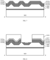
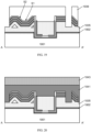
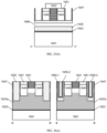
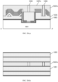
- FIG. 1 to FIG. 29(b) show schematic diagrams of some stages in a process of manufacturing a multi-bridge channel semiconductor device according to an embodiment of the present disclosure.
- the substrate 1001 may be a substrate in various forms, including but not limited to a bulk semiconductor material substrate such as a bulk Si substrate, a semiconductor-on-insulator (SOI) substrate, a compound semiconductor substrate such as a SiGe substrate, and the like.
- a bulk Si substrate is taken as an example for description.
- the substrate 1001 may have a substantially flat top surface.
- the top surface may be referred to as a horizontal surface of the substrate 1001.
- the substrate 1001 may be a (100) wafer, so that the horizontal surface of the substrate 1001 may be one of ⁇ 100 ⁇ crystal plane families.
- a position defining layer 1002 and a position maintaining layer 1004 may be sequentially formed on the substrate 1001 by, for example, an epitaxial growth.
- the position defining layer 1002 may define a bottom position of an isolation layer in a subsequent etching, and a thickness of the position defining layer is, for example, about 5 nm to 20 nm; the position maintaining layer 1004 may define a space occupied by the isolation layer, and a thickness of the position maintaining layer is, for example, about 20 nm to 150 nm.
- the position maintaining layer 1004 may have a substantially flat top surface parallel to the horizontal surface of the substrate.
- Adjacent layers in the substrate 1001, the position defining layer 1002, and the position maintaining layer 1004 may have an etching selectivity relative to each other.
- the substrate 1001 may be a silicon wafer
- the position defining layer 1002 may contain SiGe (an atomic percent of Ge is, for example, about 20% to 50%)
- the position maintaining layer 1004 may contain Si.
- both the substrate 1001 and the position maintaining layer 1004 contain Si, so that the position defining layer 1002 may define an etch stop position when the position maintaining layer 1004 is selectively etched below.
- the position defining layer 1002 may also be omitted when the substrate 1001 and the position maintaining layer 1004 contain materials having an etching selectivity relative to each other.
- a hard mask layer 1005 may be formed on the position maintaining layer 1004 by, for example, deposition.
- the hard mask layer 1005 may contain a nitride (e.g., silicon nitride) with a thickness of about 50 nm to 150 nm.
- a thin (e.g., with a thickness of about 2 nm to 10 nm) etch stop layer 1003 of an oxide (e.g., silicon oxide) or other materials may also be formed by, for example, deposition.
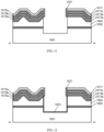
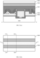
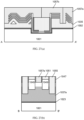
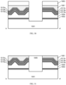
- the flat top surface of the position maintaining layer 1004 may be patterned to have an inclined configuration.
- an etching recipe with an etching selectivity for a certain crystal plane orientation may be used to obtain an inclined surface in the crystal plane orientation.
- a more general etching solution may be used.
- a stepped pattern may be formed on the top surface of the position maintaining layer 1004, and then a sharp portion of the stepped pattern may be smoothed to form an inclined surface.
- the inclination may be controlled by controlling a height of a step and/or a spacing between adjacent steps in the stepped pattern. In general, the higher the height of the step, the steeper the step; the smaller the spacing between adjacent steps, the steeper the step.
- the stepped pattern may be formed in various ways. For example, a portion of the surface of the position maintaining layer 1004 may be shielded with a photoresist, and the position maintaining layer 1004 may be etched by using the photoresist as a mask. Then, the photoresist is trimmed, and the position maintaining layer 1004 is etched by using the trimmed photoresist as a mask. The trimming and etching processes may be repeated a plurality of times, so that the stepped pattern may be obtained.
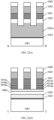
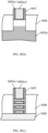
- a spacer may be used to facilitate patterning.
- a mandrel pattern may be formed on the position maintaining layer 1004 at a position to form the stepped pattern.
- the hard mask layer 1005 may be selectively etched, such as Reactive Ion Etching (RIE), by using a photoresist (not shown), so as to form a mandrel pattern 1005.
- RIE Reactive Ion Etching
- the RIE may be in a vertical direction (e.g., a direction substantially perpendicular to the surface of the substrate 1001), so that the mandrel pattern 1005 may have a vertical sidewall.
- the RIE may be stopped at the etch stop layer 1003.
- a spacer may be formed on the sidewall of the mandrel pattern 1005.
- spacers 1009a, 1009b may be formed.
- a formation of the spacer may include substantially conformally forming a spacer material layer on the position maintaining layer 1004 on which the mandrel pattern 1005 is formed by, for example, depositing, and performing an anisotropic etching, such as RIE in the vertical direction, on the formed spacer material layer.
- thicknesses (measured in a horizontal direction in the drawing) of the spacers 1009a, 1009b or a thickness of the deposited spacer material layer may be determined at least in part by an inclination to be achieved.
- the thickness of the deposited spacer material layer may be about 3 nm to 20 nm.
- two spacers 1009a and 1009b are formed on each of the opposite sidewalls of the mandrel pattern 1005.
- the present disclosure is not limited to this. There may be more or less spacers.
- the number of the spacers 1009a, 1009b may be determined according to the number of steps to be achieved (depending at least in part on a range of the inclined surface to be achieved).
- the spacers 1009a, 1009b may contain the same material, and may contain the same material as that of the mandrel pattern 1005, such as a nitride.
- etch stop layers 1007a, 1007b may be provided between the spacers and between the spacer and the mandrel pattern.
- the etch stop layers 1007a, 1007b may be thin layers (e.g., with a thickness of about 1 nm to 3 nm), such as oxide layers, having an etching selectivity relative to the spacer and the mandrel pattern.
- the etch stop layers 1007a, 1007b may be respectively deposited before the spacer material layers are deposited.
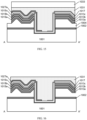
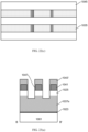
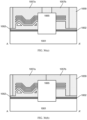
- the position maintaining layer 1004 may be etched by using the thus formed mandrel pattern 1005 and the spacers 1009a, 1009b to form the stepped pattern.
- the process is similar to the above-mentioned processes of repeatedly trimming the photoresist and etching the substrate, except that in each trimming process, a pair of spacers on the opposite sidewalls of the mandrel pattern may be controllably removed.
- the etch stop layers 1007b, 1007a, and 1003 may be selectively etched sequentially by, for example, RIE in the vertical direction, so as to expose the surface of the position maintaining layer 1004. Then, the exposed portion of the position maintaining layer 1004 may be selectively etched to a certain depth by, for example, RIE in the vertical direction.
- An etch depth (referred to herein to as a "first depth") may be determined according to the height of the step in the stepped pattern to be formed (depending at least in part on the inclination to be achieved).
- the spacer 1009b may be selectively etched isotropically so as to be removed.
- the etching of the spacer 1009b may be stopped at the etch stop layer 1007b.
- the etch stop layers 1007b, 1007a and the etch stop layer 1003 located below exposed by a removal of the spacer 1009b may be selectively etched by, such as RIE, so as to further expose the surface of the position maintaining layer 1004.
- the exposed portion of the position maintaining layer 1004 may be selectively etched to a certain depth (herein referred to as a "second depth", which may be the same as the first depth) through the process described in combination with FIG. 4 .
- a current etch depth of the position maintaining layer portion in FIG. 5 newly exposed by the removal of the spacer 1009b may be the second depth, so that the stepped pattern may be formed.
- the spacer 1009a may be further removed and etched again, so that the number of steps may be increased.
- the stepped pattern is formed on the surface of the position maintaining layer 1004.
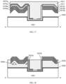
- the stepped pattern thus formed may be smoothed to obtain an inclined surface.
- an ion etching and/or bombardment may be performed on the surface of the position maintaining layer 1004 to smooth a sharp portion of the stepped pattern, so that an inclined surface may be obtained.
- the ion etching and/or bombardment may be performed in combination with the RIE process performed on the position maintaining layer 1004 after the innermost spacer 1009a is removed.
- an energy of plasmas may be adjusted to achieve a smooth inclined surface (e.g., due to a scattering of Ar or N atoms/ions).
- the inclination may be controlled by controlling etch depths, such as the first depth and the second depth, as described in connection with FIG. 4 and FIG. 5 , so as to optimize an area occupied by the device and the device performance (e.g., a carrier mobility, on-current, or the like).
- the inclined surface may be one of ⁇ 110 ⁇ crystal plane families.
- the mandrel pattern 1005 and the remaining etch stop layers may be removed by a selective etching.
- a wet etching may be used.
- the mandrel pattern 1005 of nitride may be etched by using a hot phosphoric acid solution, and the etch stop layers of oxide may be etched by using hydrochloric acid or a buffered oxide etchant (BOE).
- BOE buffered oxide etchant
- the device may be manufactured on the position maintaining layer 1004 having an inclined configuration on a surface thereof.
- an alternating stack layer of sacrificial layers 1013a, 1013b, 1013c and channel layers 1015a, 1015b, 1015c may be formed on the surface of the position maintaining layer 1004 by, for example, an epitaxial growth.
- the channel layers 1015a, 1015b, 1015c may then form nanosheets of a channel portion, with a thickness of, for example, about 3 nm to 15 nm.
- an in-situ doping may be performed to adjust a device threshold.
- the sacrificial layers 1013a, 1013b, 1013c may define a gap between the lowermost nanosheet and the substrate 1001 and a gap between adjacent nanosheets, with a thickness of, for example, about 5 nm to 20 nm.
- the lowermost sacrificial layer 1013a may be relatively thick, for example, about 2nm to 5nm thicker than the other sacrificial layers 1013b, 1013c.
- the number of the sacrificial layers and the channel layers in the alternating stack layer may be changed according to a device design, for example, the number may be more or less.
- the position maintaining layer 1004 and adjacent layers in the above-mentioned layers formed thereon may have an etching selectivity relative to each other.
- the sacrificial layer 1013a may contain a material similar to or the same as that of the position defining layer 1002, and thus may have a similar or same etching selectivity for the same etching recipe subsequently.
- the sacrificial layers 1013a, 1013b, 1013c may contain SiGe with an atomic percentage of Ge of about 20% to 50%, which is substantially the same as or close to that in the position defining layer 1002.
- the channel layers 1015a, 1015b, 1015c may contain Si.
- the channel layers 1015a, 1015b, 1015c may have shapes extending along the surface of the position maintaining layer 1004 and thus have surfaces that are inclined or not parallel relative to the horizontal surface of the substrate 1001.
- the channel layers 1015a, 1015b, 1015c and the sacrificial layers 1013a, 1013b, 1013c may each be formed substantially conformally on the surface of the position maintaining layer 1004 and may have a substantially uniform thickness.
- the inclined surfaces of the channel layers 1015a, 1015b, 1015c may be consistent with the inclined configuration of the position maintaining layer 1004, and thus be, for example, one of the ⁇ 110 ⁇ crystal plane families.
- the isolation layer may be formed by replacing the position maintaining layer 1004 with a dielectric material. During the replacement, there is a process in which the stack is suspended relative to the substrate. In order to maintain the stack layer, a vertical structure connected to the substrate may be formed to support the stack layer. For the same device region, a vertical structure may be formed on one side, and the other side may be exposed for performing the replacement process. Respective vertical structures of adjacent devices may be located therebetween and may be formed together.
- a photoresist 1019 may be formed on the stack layer and patterned to expose a region between some adjacent devices.
- an oxide layer 1017 (with a thickness of, for example, about 5 nm to 20 nm) may be formed on the top surface of the stack layer to protect a surface of the stack layer, for example, prevent the surface from being damaged by processes such as oxidation and cleaning when removing the photoresist 1019.
- the oxide layer 1017 and each layer in the stack layer are selectively etched sequentially, such as RIE, by using the photoresist 1019 as a mask, so as to form a trench (which may be referred to as a first trench) penetrating the stack layer.
- a formation of one trench is taken as an example for description.
- the present disclosure is not limited to this. For example, more or fewer trenches may be formed.
- a vertical structure may be formed in the first trench to support stack layers on two sides of the first trench.
- an etch stop layer (see 1023 in FIG. 12 ) may be formed in the trench first, and then the vertical structure is formed.
- the etch stop layer may not exist on a sidewall of the channel layer considering that the vertical structure and the channel layer may be connected with each other to form the channel portion of the device together. That is, the etch stop layer may be formed at a lower portion of the trench without covering the sidewall of the stack layer or the channel layer in the stack layer (see FIG. 12 ).
- the trench may be formed in stages.
- the etch depth may be controlled, so that the sidewall of each layer in the stack layer may be exposed (a certain process margin is considered at the same time), but the etching does not proceed too much into the position maintaining layer 1004.
- the photoresist 1019 may be removed.
- the etch depth defines an upper portion of the trench where an etch stop layer does not need to be formed.
- a protective layer 1021 may be formed on a sidewall of the upper portion of the thus defined trench, as shown in FIG. 9 , so as to prevent the sidewall from being affected in the subsequent processing.
- the protective layer 1021 may be formed through a spacer process, and may contain a nitride with a thickness of, for example, about 1 nm to 5 nm.
- the trench may be deepened by further etching such as RIE.
- the etch depth may be controlled to extend the trench into the substrate 1001, so that the subsequently formed vertical structure may be connected to the substrate 1001 and thus may be used as a support structure to support the stack layer especially during the process of removing the position maintaining layer 1004.
- the etch depth here defines a lower portion of the trench where an etch stop layer may be formed.
- a sidewall the lower portion of the trench may be recessed relative to the sidewall of the upper portion of the trench by etching back with an etch back depth of, for example, about 5 nm to 10 nm.
- the trench that is etched back should not expose the channel layer (especially the lowermost channel layer 1015a) in the stack layer, that is, the lowermost sacrificial layer 1013a should not be etched off, so that the lowermost sacrificial layer 1013a may effectively function as an etch stop during the process of removing the position maintaining layer 1004. In this way, a desired first trench may finally be obtained.
- An etch stop layer may be formed in the recess.
- an etch stop layer 1023 may be formed on a surface of the lower portion of the trench by a selective epitaxy. The selective epitaxial growth may not occur on a surface of the protective layer 1021.
- the grown etch stop layer 1023 may be controlled to have a thin thickness of, for example, about 2 nm to 5 nm, so that the grown etch stop layer 1023 may not extend to the protective layer 1021.
- the etch stop layer 1023 may contain a material similar to or the same as that of the sacrificial layer 1013a and the position defining layer 1002, and thus may subsequently have a similar to or same etch selectivity for the same etching recipe.
- the etch stop layer 1023 may contain SiGe with an atomic percentage of Ge of about 20% to 50%, which is substantially the same as or close to that in the sacrificial layer 1013a and the position defining layer 1002.
- the position maintaining layer 1014 is covered by the position maintaining layer 1012 on a lower side, and covered by the sacrificial layer 1013a on an upper side.
- One side in a horizontal direction of the position maintaining layer 1014 is covered by the etch stop layer 1023, and the other side in the horizontal direction may be subsequently exposed (so as to be removed).
- the protective layer 1021 may be removed by a selective etching.
- a wet etching such as a hot phosphoric acid solution, may be used.
- the sidewall of each layer in the stack layer may be exposed in the upper portion of the trench.
- a semiconductor layer 1025 may be formed by, for example, a selective epitaxial growth, in the trench with the etch stop layer formed on a lower surface of the trench.
- the semiconductor layer 1025 extends along a surface of the trench so as to present a U shape, two opposite arms of the U-shape may be respectively used as vertical structures of the corresponding device.
- the semiconductor layer 1025 may be connected with each channel layer.
- the semiconductor layer 1025 (especially an upper portion thereof) may also be used (together with the channel layer) as the channel portion (similar to a fin) of the device, and thus may contain the same material as that of the channel layer such as Si, with a thickness of, for example, about 3 nm to 10 nm.
- a punch-through stopper may be formed in a lower portion (e.g., a portion below a top surface of a subsequently formed isolation layer, that is, a portion below a portion of the semiconductor layer 1025 serving as the channel portion) of the semiconductor layer 1025 (see 1037a, 1037b shown in FIG. 18 ).
- the PTS may be achieved by doping the lower portion of the semiconductor layer 1025 with a conductivity type opposite to that of the device.
- the doping may be achieved by, for example, a solid-phase doping.
- a first dopant source layer 1027a may be formed on the structure shown in FIG. 13 by, for example, deposition.
- the first dopant source layer 1027a may be an oxide layer containing an n-type dopant such as As or P with a concentration of about 0.1% to 5%, and a thickness of the first dopant source layer is about 1 nm to 3 nm.
- a barrier layer 1029 may be formed on the first dopant source layer 1027a by, for example, deposition.
- the barrier layer 1029 may be a nitride or an oxynitride with a thickness of about 1 nm to 3 nm.
- the first dopant source layer 1027a and the barrier layer 1029 located above may be patterned by, for example, photolithography so as to be left on the semiconductor layer 1025 (e.g., a left portion in the drawing) for a p-type device.
- a second dopant source layer 1027b may be formed.
- the second dopant source layer 1027b may be an oxide layer containing a p-type dopant such as B with a concentration of about 0.1 % to 5 %, and a thickness of the seond dopant source layer is about 1 nm to 3 nm.
- the second dopant source layer 1027b may be patterned to be left on the semiconductor layer 1025 (e.g., a right portion in the drawing) for an n-type device region.
- a simultaneous formation of a p-type device and an n-type device (and a CMOS configuration may thus be formed) is taken as an example for description.
- the present disclosure is not limited to this.
- a device of a separate conductivity type it is not necessary to separately form dopant source layers having dopants of different conductivity types.
- the first dopant source layer 1027a and the second dopant source layer 1027b respectively cover the entire vertical portion of the semiconductor layer 1025. However, only a lower portion of the vertical portion of the semiconductor layer 1025 is required to be doped to form the PTS.
- the first dopant source layer 1027a and the second dopant source layer 1027b located at the upper portion of the vertical portion of the semiconductor layer 1025 may be removed. This may be performed in combination with the formation of the isolation layer, since the upper portion and the lower portion are defined based on the top surface of the isolation layer.
- a dielectric material 1031 such as an oxide, may be formed on the substrate 1001 by, for example, deposition.
- the dielectric material 1031 may be used to fill the trench and may be used to cover the stack layer, the first dopant source layer 1027a and the second dopant source layer 1027b.
- a planarization process such as CMP may be performed on the deposited dielectric material 1031.
- a processing channel to the position maintaining layer 1004 may be formed.
- a photoresist 1033 may be formed on the dielectric material 1031 and patterned to expose a region between some adjacent device areas.
- Each layer in the stack layer (and each material layer above the stack layer) is sequentially selectively etched, such as RIE, by using the photoresist 1033 as a mask, so as to form a second trench.
- the RIE may proceed into the position maintaining layer 1004 so as to access the position maintaining layer 1004 through the second trench, but the RIE does not reach the position defining layer 1002 (which may avoid that the position maintaining layer 1004 may not be replaced due to being completely shielded by the protective layer in a case of forming a protective layer below).
- the photoresist 1033 may be removed.
- the position maintaining layer 1004 may be replaced with an insulator.
- a protective layer may be formed on the sidewall of the stack layer.
- a protective layer may be formed on the exposed sidewall of the stack layer through a spacer formation process.
- the protective layer may contain an oxide, and may thus be shown integrally with the dielectric material 1031, which is also an oxide, as 1031.
- the position maintaining layer 1004 may be removed by a selective etching.
- the vertical structure in combination with the dielectric material 1031 may be used to suspend the stack layer relative to the substrate 1001; on the other hand, the second trench may be used to form a processing channel for etching the position maintaining layer 1004 below the stack layer.
- the position maintaining layer 1004 Si in this example
- the position maintaining layer 1004 may be selectively etched relative to the position defining layer 1002, as well as the sacrificial layer 1013a and the etch stop layer 1023 (SiGe in this example) by using a TMAH solution.
- an isolation layer may be formed by filling with a dielectric.
- the sacrificial layer will be replaced with a gate stack in a subsequent replacement gate process, and the etch stop layer 1023 containing the same material as that of the sacrificial layer may also be replaced with the gate stack. This may result in an overlap of the gate stack with the lower portion of the vertical portion of the semiconductor layer 1025, which is undesirable.
- the etch stop layer 1023 exposed by the removal of the position maintaining layer 1004 may be removed.
- the etch stop layer 1023 SiGe in this example
- the semiconductor layer 1025 Si in this example
- the lowermost sacrificial layer 1013a (also Si in this example) may also be etched. However, due to a relatively thick thickness of the lowermost sacrificial layer 1013a, an amount of etching may be controlled so that the lowermost sacrificial layer 1013 may still continuously cover an entire lower surface of the channel layer 1015a.
- a dielectric material may be filled below the stack layer through the second trench to form the isolation layer.
- the filling may be performed by deposition such as a Chemical Vapor Deposition (CVD), an Atomic Layer Deposition (ALD), and the like.
- CVD Chemical Vapor Deposition
- ALD Atomic Layer Deposition
- the space below the stack layer may not be completely filled with the dielectric material, and an air gap 1006 may exist.
- a method of repeating deposition and etching may be used.
- the second trench may also be filled with a dielectric material to form an isolation portion between devices.
- the filled dielectric material may contain an oxide.
- the dielectric material may be etched back to form an isolation layer 1035.
- a top surface of the isolation layer 1035 may be close to a position where the lowermost sacrificial layer 1013a is connected with the semiconductor layer 1025 (especially a bottom surface of the lowermost sacrificial layer 1013a at the position) so as to achieve a good control of a gate on a fin. It may be shown that, on one hand, the isolation layer 1035 is disposed between adjacent devices to form an electrical isolation, such as Shallow Trench Isolation (STI), between adjacent devices; on the other hand, the isolation layer 1035 is disposed below the channel portion to suppress a leakage between a source and a drain in the same device.
- STI Shallow Trench Isolation
- the barrier layer 1029 and portions of the dopant source layers 1027a, 1027b exposed by the isolation layer 1035 may be selectively etched, such as RIE, so that they may be left below the top surface of the isolation layer 1035.
- Dopants in the dopant source layers 1027a, 1027b may be driven into the semiconductor layer 1025 by, for example, an annealing process, and PTSs 1037a, 1037b may be formed in the semiconductor layer 1025. Due to the above-mentioned processes, the dopant source layers 1027a, 1027b are left below the top surface of the isolation layer 1035, so that the formed PTSs 1037a, 1037b may not substantially exceed the top surface of the isolation layer 1035.
- a portion of the semiconductor layer 1025 located above the top surface of the isolation layer 1035 may be used as a fin.
- the stack layer has been separated between adjacent devices on the two opposite sides of the trenches. There may be some stack layers between adjacent devices that have not been separated (e.g., the stack layer on a right side in FIG. 18 may be separated into portions for two devices).
- the stack layer may be separated according to a device layout design. For example, as shown in FIG. 19 , a photoresist 1039 may be formed on the stack layer and the isolation layer and patterned to expose a region between adjacent devices that have not been separated.
- the photoresist 1039 may also expose a position of the second trench, so that the top surface of the isolation layer 1035 in the second trench may be lowered to expose an entire side surface of the stack layer.
- a gate stack formed subsequently may surround all the channel layers.
- a thin oxide layer (not shown) may be formed on the top surface of the stack layer to protect the surface of the stack layer.
- the stack layer may be selectively etched, such as RIE, by using the photoresist 1039 as a mask, so as to separate the stack layer between different device regions.
- the RIE may proceed into the isolation layer 1035 so as to fully expose the sidewall of the stack layer, thereby forming a third trench.
- the first trench, the second trench, and the third trench may all have stripe shapes extending in the first direction (a direction entering a paper surface in the drawing), so that the stack layer may be divided into stripe shapes extending in the first direction for each device. After that, the photoresist 1039 may be removed.
- the nanosheet may have a surface S1 parallel to the horizontal surface of the substrate 1001 and a surface S2 not parallel to the horizontal surface of the substrate 1001, so that the nanosheet is in a shape of a broken line.
- the nanosheet may also have a surface parallel to the horizontal surface of the substrate 1001 and a surface not parallel to the horizontal surface of the substrate 1001, so that the nanosheet is in a shape of a broken line.
- some of the channel layers may have a shape of an oblique straight line that is not parallel to the horizontal surface of the substrate 1001 rather than the shape of a broken line.
- the shape of the broken line is not limited to have a plurality of inflection points as shown in the drawing, but may have a single inflection point.
- the channel portion has a surface parallel to the horizontal surface of the substrate 1001.
- a combination of a device with a vertical structure and a device without a vertical structure may be formed on the substrate through arrangements of the first trench, the second trench, and the third trench.
- the surface parallel to the horizontal surface of the substrate may be one of the ⁇ 100 ⁇ crystal plane families, and the surface not parallel to the horizontal surface of the substrate may be one of the ⁇ 110 ⁇ crystal plane families.
- the surface parallel to the horizontal surface of the substrate may be one of the ⁇ 110 ⁇ crystal plane families, and the surface not parallel to the horizontal surface of the substrate may be one of the ⁇ 100 ⁇ crystal plane families.
- the ⁇ 100 ⁇ crystal plane family is beneficial to a mobility of electrons. Therefore, a channel portion whose surface is mainly of the ⁇ 100 ⁇ crystal plane families (e.g., a middle region in FIG. 19 in a case of the (100) wafer) may be used to manufacture an n-type device.
- the ⁇ 110 ⁇ crystal plane family is beneficial to a mobility of holes. Therefore, a channel portion whose surface is mainly of the ⁇ 110 ⁇ crystal plane families (e.g., the rightmost region in FIG. 19 in a case of the (100) wafer) may be used to manufacture a p-type device.
- the leftmost region in FIG. 19 has surfaces of both the ⁇ 100 ⁇ and ⁇ 110 ⁇ crystal plane families, thus may be used to manufacture the p-type device or the n-type device (p-type device in this example).
- a sacrificial gate layer 1041 may be formed on the isolation layer 1035.
- the sacrificial gate layer 1041 may contain a material similar to or the same as that of the sacrificial layers 1013a, 1013b, 1013c, so that the sacrificial gate layer 1041 may be etched by the same etching recipe later.
- the sacrificial gate layer 1041 may contain SiGe with an atomic percentage of Ge of about 20% to 50%, which is substantially the same as or close to that in the sacrificial layers 1013a, 1013b, 1013c.
- the sacrificial gate layer 1041 may be formed by deposition and then planarization such as CMP.
- a hard mask layer 1043 may be formed on the sacrificial gate layer 1041 by, for example, deposition, so as to facilitate a subsequent patterning of the sacrificial gate layer 1041.
- the hard mask layer 1043 may contain a nitride.
- the sacrificial gate layer 1041 may be patterned into a stripe shape extending in a second direction (a horizontal direction on a paper surface in the drawing) intersecting (e.g., perpendicular to) the first direction so as to form the sacrificial gate.
- a photoresist 1045 may be formed on the hard mask layer 1043 and patterned into stripe shapes extending in the second direction (see a top view in FIG. 21(b) ). Then, as shown in FIG. 22(a), FIG. 22(b) and FIG.
- the hard mask layer 1043 and the sacrificial gate layer 1041 may be selectively etched sequentially by, for example, RIE, by using the photoresist 1045 as a mask.
- the sacrificial gate layer 1041 is patterned into stripe shapes extending in the second direction.
- the channel layer and the sacrificial layer exposed by the removal of the sacrificial gate layer 1019 in the stack layer may also be selectively etched sequentially, such as RIE, so that the stack layer is left below the sacrificial gate layer 1019.
- the semiconductor layer 1025 may also be etched to form a fin left below the sacrificial gate layer 1019. The etching may be stopped at the isolation layer 1035 of the oxide. After that, the photoresist 1045 may be removed.
- the current sacrificial gate layer 1041 and the sacrificial layers 1013a, 1013b, 1013c surround the channel layers 1015a, 1015b, 1015c, thus define a space subsequently used for the gate stack.
- a gate spacer may be formed on sidewalls of the sacrificial gate layer 1041, and the sacrificial layers 1013a, 1013b, and 1013c.
- the sacrificial gate layer 1041 and the sacrificial layers 1013a, 1013b, 1013c may be recessed by a certain recess depth of, for example, about 2 nm to 7 nm (relative to the channel layers 1015a, 1015b, 1015c) by a selective etching.
- an Atomic Layer Etching ALE
- a dielectric material may be filled in the recess thus formed to form a gate spacer 1047.
- the filling may be formed by, for example, depositing a nitride with a thickness of about 3 nm to 10 nm and then performing RIE on the deposited nitride (until a surface of the channel layer is exposed).
- the hard mask layer 1043 which is also an nitride, may be integrated with the gate spacer on the sidewall of the sacrificial gate layer 1041, and may thus be marked as 1043'.
- the gate spacer 1047 may be self-aligned and formed on the sidewall of the sacrificial gate layer 1041 and the sacrificial layers 1013a, 1013b, 1013c, but not formed on the sidewall of the channel layers 1015a, 1015b, 1015c.
- the gate spacer 1047 may have a substantially uniform thickness which, for example, depends on the depth of the above-mentioned recess.
- an outer sidewall of the gate spacer 1047 may be substantially vertically aligned with the outer sidewall of the channel layers 1015a, 1015b, 1015c, and an inner sidewall of the gate spacer 1047 may be substantially aligned in the vertical direction (by controlling the etch depth to be substantially the same at each position when forming the recess).
- source/drain portions connected with the sidewalls of the semiconductor layer 1025 and the channel layers 1015a, 1015b, and 1015c may be formed on two sides of the sacrificial gate layer 1041.
- source/drain portions 1049 may be formed by, for example, an epitaxial growth.
- the source/drain portions 1049 may be grown from a surface of the exposed semiconductor layer 1025 and surfaces of the channel layers 1015a, 1015b, 1015c.
- the grown source/drain portions 1049 are connected with the surface of the semiconductor layer 1025 and the sidewalls of the channel layers 1015a, 1015b, and 1015c.
- the source/drain portion 1049 may be in-situ doped to a conductivity type corresponding to the device to be formed, e.g., an n-type for an n-type device and a p-type for a p-type device, and a doping concentration may be about 1E19cm -3 to 1E21cm -3 .
- the grown source/drain portion 1049 may contain a different material (e.g., having a different lattice constant) from that of the semiconductor layer and the channel layer, so as to apply a stress to the channel layer.
- the source/drain portion 1049 may contain Si:C (an atomic percent of C is, for example, about 0.1 % to 5%); for a p-type device, the source/drain portion 1049 may contain SiGe (an atomic percent of Ge is, for example, about 20% to 75%).
- the source/drain portions may be grown separately for the n-type device and the p-type device.
- a shielding layer such as a photoresist or the like.
- the same source/drain portion 1049 is connected to the semiconductor layer 1025 and the channel layers 1015a, 1015b, 1015c on two opposite sides. That is, the devices on the two sides are currently electrically connected together. An electrical isolation may be provided between devices according to the design layout.
- a dielectric material 1051 such as an oxide may be deposited on the substrate 1001 to cover the sacrificial gate layer 1041, the source/drain portions 1049 and the isolation layer 1035.
- a planarization process such as CMP may be performed on the dielectric material 1051 to expose the sacrificial gate layer 1041.
- a photoresist 1053 may be formed on the dielectric material 1051 and patterned to shield one or more sacrificial gate layers 1041, and exposing other sacrificial gate layers 1041. In this example, the sacrificial gate layer 1041 in the middle is shielded, while the sacrificial gate layer 1041 on two sides is exposed.
- the exposed sacrificial gate layer 1041, and the semiconductor layer 1025, the channel layers and the sacrificial layers located below may be selectively etched sequentially by, for example, RIE, thereby leaving a space between the gate spacers 1047.
- the etching may proceed into the PTSs 1037a, 1037b to achieve a good electrical isolation.
- the photoresist 1053 may be removed.
- a dielectric material 1055 such as an oxide, may be filled in the space left.
- the filling of the dielectric material 1055 may include deposition and then planarization.
- a multilayer dielectric layer may be formed in the above-mentioned space by, for example, a sequential deposition.
- a stacked structure of multilayer dielectrics 1055-1, 1055-2, 1055-3 may be formed.
- the dielectric layer 1055-1 may contain an oxide
- the dielectric layer 1055-2 may contain a nitride
- the dielectric layer 1055-3 may contain an oxynitride.
- the present disclosure is not limited to this. For example, more or fewer dielectric layers may be formed, and the dielectric layers may contain other materials.
- a replacement gate process may be performed to complete a device manufacturing.
- the sacrificial gate layer 1041 and the sacrificial layers 1013a, 1013b, and 1013c may be removed by a selective etching (as described above, they may be removed by the same etching recipe), so that a space may be formed inside the gate spacer 1047, and a gate stack may be formed in the space.
- a p-type device and an-type device are simultaneously formed on the substrate, so different gate stacks 1057a, 1057b may be formed for the p-type device and n-type device, respectively. For example, they have work functions different from each other.
- a region of the type of device may be shielded by a shielding layer such as a photoresist.
- a first gate stack existing in a region of another type of device may be removed (only a gate conductor layer may be removed), and then a second gate stack for the another type of device may be formed.
- the gate stack 1057a for the p-type device may include a gate dielectric layer 1057a-1 and a gate conductor layer 1057a-2
- the gate stack 1057b for the n-type device may include a gate dielectric layer 1057b-1 and a gate conductor layer 1057b-2 (see FIG. 28 (a) , FIG. 28 (b) and FIG.
- the gate dielectric layers 1057a-1, 1057b-1 may be formed in a substantially conformal manner, with a thickness of, for example, about 2 nm to 5 nm, and may include a high-k gate dielectric such as HfO 2 . Before the high-k gate dielectric is formed, an interface layer may also be formed on the surface of the channel layer, e.g., an oxide formed by an oxidation process or deposition such as an Atomic Layer Deposition (ALD), with a thickness of about 0.2 nm to 2 nm.
- ALD Atomic Layer Deposition
- the gate conductor layers 1057a-2, 1057b-2 may contain a work function adjustment metal such as TiN, TaN, etc., and a gate conductive metal such as W, etc.
- FIG. 28(a) , FIG. 28(b) and FIG. 28(c) more clearly show the gate stack portions around the semiconductor layer 1025 and the channel layers in an enlarged form. It may be shown that the gate stack is located inside the gate spacer 1047 surrounding each of the channel layers 1015a, 1015b and 1015c.
- the channel layers 1015a, 1015b, and 1015c are connected to the source/drain portions 1049 on two sides, respectively, and a channel is formed between the source/drain portions 1049.
- the gate stack may surround the sidewall and the top surface of the upper portion of the semiconductor layer 1025, the semiconductor layer 1025 is also connected to the source/drain portions 1049 on two sides, and a channel is formed between the source/drain portions 1049, which is similar to a FinFET.
- the channel layers 1015a, 1015b, 1015c are more mechanically stable e.g., are not easily bent or adhered during the removal of the sacrificial layers 1013a, 1013b, 1013c, which is beneficial to improve a yield rate.
- the gate stacks of current devices are continuous with each other, so that respective gates of the devices are electrically connected to each other.
- An electrical isolation may be provided between the devices according to the design layout.
- a photoresist (not shown) may be formed on the dielectric materials 1051, 1055 to expose the gate stacks 1057a, 1057b between device regions to be isolated, while the rest of the gate stacks 1057a, 1057b are shielded.
- the exposed gate stacks 1057a, 1057b (especially the gate conductor layers 1057a-2, 1057b-2) may be selectively etched such as RIE. The etching may be stopped at the isolation layer 1035 (or stopped at the gate dielectric layers 1057a-1, 1057b-1) located below.
- a dielectric material 1059 such as an oxide may be filled in a space left by an etching of the exposed portions of the gate stacks 1057a, 1057b. The filling of the dielectric material 1059 may include deposition and then planarization.
- the vertical structure not only plays a supporting role, but is also used to form a device channel.
- the present disclosure is not limited to this.
- the vertical structure may only function as a support portion.
- FIG. 30 to FIG. 36(b) show schematic diagrams of some stages in a process of manufacturing a semiconductor device according to another embodiment of the present disclosure. Differences from the above-mentioned embodiments will be mainly described below.
- the processes described above with reference to FIG. 1 to FIG. 7 may be performed, so that an alternating stack layer of sacrificial layers 1013a, 1013b, 1013c and channel layers 1015a, 1015b, 1015c may be formed on the position maintaining layer 1004.
- the first trench may be formed in stages.
- the first trench may be simply formed.
- an oxide layer 1061 (with a thickness of, for example, about 10 nm to 200 nm) may be formed on the top surface of the stack layer and planarized such as CMP.
- a photoresist 1063 may be formed on a top surface of the oxide layer 1061 and patterned to expose a region (a region to form the first trench) between some adjacent devices.
- the oxide layer 1061 and each layer in the stack layer are selectively etched sequentially, such as RIE, by using the photoresist 1063 as a mask, so as to form a first trench penetrating the stack layer.
- the first trench may extend into the substrate 1001, so that a subsequently formed vertical structure may be connected to the substrate 1001 and thus may be used as a support structure to support the stack layer. After that, the photoresist 1063 may be removed.
- a dielectric material 1065 such as SiC may be formed on the substrate 1001 by, for example, deposition.
- the dielectric material 1065 may be used to fill the first trench and may cover the oxide layer 1061.
- a planarization process such as CMP may be performed on the deposited dielectric material 1065 and may be stopped at the oxide layer 1061.
- the dielectric material 1065 filled in the first trench may form a vertical structure that is used as a support portion.
- a replacement of the position maintaining layer 1004 may be performed.
- the replacement process may be the same as that in the above-mentioned embodiments.
- a photoresist 1067 may be formed on the oxide layer 1061 and the dielectric material 1065 and patterned to expose a region (a region to form a second trench) between some adjacent device regions.
- Each layer in the stack layer (and each material layer above the stack layer) may be selectively etched sequentially, such as RIE, by using the photoresist 1067 as a mask, so as to form the second trench.
- the RIE may proceed into the position maintaining layer 1004 so as to access the position maintaining layer 1004 through the second trench, but the RIE does not reach the position defining layer 1002 (which may avoid that the position maintaining layer 1004 may not be replaced due to being completely shielded by a protective layer in a case of forming the protective layer below). After that, the photoresist 1067 may be removed.
- a protective layer may be formed on the sidewall of the stack layer.
- a protective layer may be formed on the exposed sidewall of the stack layer through a spacer formation process.
- the protective layer may contain an oxide, and may thus be shown integrally with the dielectric material 1061, which is also an oxide, as 1061'.
- the position maintaining layer 1004 may be removed by a selective etching.
- the vertical structure 1065 may suspend the stack layer relative to the substrate 1001; on the other hand, the second trench may form a processing channel for etching the position maintaining layer 1004 located below the stack layer.
- the position maintaining layer 1004 Si in this example
- the vertical structure 1065 SiC in this example
- the position defining layer 1002 and the sacrificial layer 1013a SiGe in this example
- an isolation layer may be formed by filling with a dielectric.
- a space below the stack layer may be may be filled a dielectric material through the second trench so as to form an isolation layer 1035.
- a top surface of the isolation layer 1035 may be as low as to expose the sidewall of each layer in the stack layer, since there is no need to consider a fin.
- the top surface of the isolation layer 1035 may be higher than the position defining layer 1002 for an effective isolation, and may be lower than the lowermost surface of the stack layer for a subsequent processing (e.g., the removal of the sacrificial layer) of the stack layer. It may be shown that, on one hand, the isolation layer 1035 is disposed between adjacent devices to form an electrical isolation such as a Shallow Trench Isolation (STI) between the adjacent devices; on the other hand, the isolation layer 1035 is disposed below the channel portion so as to suppress a leakage between a source and a drain in the same device.
- STI Shallow Trench Isolation
- the third trench is not formed. Adjacent devices may be separated from each other by the first trench and the second trench.
- FIG. 36(a) shows a case where respective gate electrodes of adjacent p-type and n-type devices are electrically isolated
- FIG. 36(b) shows a case where respective gate electrodes of adjacent p-type and n-type devices are electrically connected to form a CMOS configuration.
- the semiconductor device may be applied to various electronic apparatuses.
- an integrated circuit IC
- the present disclosure further provides an electronic apparatus including the above-mentioned semiconductor device.
- the electronic apparatus may further include a display screen cooperating with the integrated circuit, a wireless transceiver cooperating with the integrated circuit, and other components.
- the electronic apparatus may include, for example, a smart phone, a computer, a Personal Computer (PC), an artificial intelligence apparatus, a wearable apparatus, a mobile power supply, etc.
- SoC System on Chip
- the method may include the above-mentioned method.
- various devices may be integrated on a chip, and at least some of which are manufactured according to the method of the present disclosure.
Applications Claiming Priority (2)
| Application Number | Priority Date | Filing Date | Title |
|---|---|---|---|
| CN202010282959.4A CN111463287B (zh) | 2020-04-10 | 2020-04-10 | 半导体器件及其制造方法及包括其的电子设备 |
| PCT/CN2021/079955 WO2021203899A1 (fr) | 2020-04-10 | 2021-03-10 | Dispositif à semi-conducteur, son procédé de fabrication, et dispositif électronique le comprenant |
Publications (1)
| Publication Number | Publication Date |
|---|---|
| EP4135052A1 true EP4135052A1 (fr) | 2023-02-15 |
Family
ID=71678612
Family Applications (1)
| Application Number | Title | Priority Date | Filing Date |
|---|---|---|---|
| EP21784634.4A Pending EP4135052A1 (fr) | 2020-04-10 | 2021-03-10 | Dispositif à semi-conducteur, son procédé de fabrication, et dispositif électronique le comprenant |
Country Status (5)
| Country | Link |
|---|---|
| US (1) | US20230223444A1 (fr) |
| EP (1) | EP4135052A1 (fr) |
| KR (1) | KR20220163469A (fr) |
| CN (1) | CN111463287B (fr) |
| WO (1) | WO2021203899A1 (fr) |
Families Citing this family (3)
| Publication number | Priority date | Publication date | Assignee | Title |
|---|---|---|---|---|
| CN111463287B (zh) * | 2020-04-10 | 2024-02-27 | 中国科学院微电子研究所 | 半导体器件及其制造方法及包括其的电子设备 |
| CN111446292B (zh) * | 2020-04-10 | 2024-04-26 | 中国科学院微电子研究所 | 半导体器件及其制造方法及包括其的电子设备 |
| US20230420574A1 (en) * | 2022-06-23 | 2023-12-28 | Intel Corporation | Mobility improvement in gate all around transistors based on substrate orientation |
Family Cites Families (12)
| Publication number | Priority date | Publication date | Assignee | Title |
|---|---|---|---|---|
| KR100604908B1 (ko) * | 2004-10-11 | 2006-07-28 | 삼성전자주식회사 | 이종의 게이트 절연막을 구비하는 씬-바디 채널 씨모스소자 및 그 제조방법 |
| US7190050B2 (en) * | 2005-07-01 | 2007-03-13 | Synopsys, Inc. | Integrated circuit on corrugated substrate |
| US7456450B2 (en) * | 2006-02-09 | 2008-11-25 | International Business Machines Corporation | CMOS devices with hybrid channel orientations and method for fabricating the same |
| US7566949B2 (en) * | 2006-04-28 | 2009-07-28 | International Business Machines Corporation | High performance 3D FET structures, and methods for forming the same using preferential crystallographic etching |
| CN101719501B (zh) * | 2009-12-01 | 2011-07-20 | 中国科学院上海微系统与信息技术研究所 | 混合晶向反型模式全包围栅cmos场效应晶体管 |
| US9741811B2 (en) * | 2014-12-15 | 2017-08-22 | Samsung Electronics Co., Ltd. | Integrated circuit devices including source/drain extension regions and methods of forming the same |
| KR102527382B1 (ko) * | 2016-06-21 | 2023-04-28 | 삼성전자주식회사 | 반도체 소자 |
| US10741558B2 (en) * | 2018-08-14 | 2020-08-11 | Taiwan Semiconductor Manufacturing Co., Ltd. | Nanosheet CMOS device and method of forming |
| CN109411539B (zh) * | 2018-10-26 | 2022-04-19 | 中国科学院微电子研究所 | 半导体器件及其制造方法及包括该半导体器件的电子设备 |
| CN110034015B (zh) * | 2019-04-19 | 2021-07-23 | 中国科学院微电子研究所 | 一种纳米线围栅器件的形成方法 |
| CN111463287B (zh) * | 2020-04-10 | 2024-02-27 | 中国科学院微电子研究所 | 半导体器件及其制造方法及包括其的电子设备 |
| CN111446292B (zh) * | 2020-04-10 | 2024-04-26 | 中国科学院微电子研究所 | 半导体器件及其制造方法及包括其的电子设备 |
-
2020
- 2020-04-10 CN CN202010282959.4A patent/CN111463287B/zh active Active
-
2021
- 2021-03-10 EP EP21784634.4A patent/EP4135052A1/fr active Pending
- 2021-03-10 WO PCT/CN2021/079955 patent/WO2021203899A1/fr unknown
- 2021-03-10 KR KR1020227038605A patent/KR20220163469A/ko unknown
- 2021-03-10 US US17/995,907 patent/US20230223444A1/en active Pending
Also Published As
| Publication number | Publication date |
|---|---|
| US20230223444A1 (en) | 2023-07-13 |
| CN111463287B (zh) | 2024-02-27 |
| WO2021203899A1 (fr) | 2021-10-14 |
| KR20220163469A (ko) | 2022-12-09 |
| CN111463287A (zh) | 2020-07-28 |
Similar Documents
| Publication | Publication Date | Title |
|---|---|---|
| CN111584486B (zh) | 具有交错结构的半导体装置及其制造方法及电子设备 | |
| EP4135052A1 (fr) | Dispositif à semi-conducteur, son procédé de fabrication, et dispositif électronique le comprenant | |
| CN111106111B (zh) | 半导体装置及其制造方法及包括该半导体装置的电子设备 | |
| US20230135187A1 (en) | Semiconductor device, method of manufacturing the same, and electronic apparatus including the same | |
| US20220416047A1 (en) | Semiconductor device, method for manufacturing semiconductor device, and electronic apparatus including the semiconductor device | |
| WO2021103910A1 (fr) | Dispositif à semi-conducteur et son procédé de fabrication, et dispositif électronique comprenant ledit dispositif à semi-conducteur | |
| US20230187560A1 (en) | Semiconductor device having zigzag structure, method of manufacturing semiconductor device, and electronic device | |
| US20240030313A1 (en) | Device having ferroelectric or negative capacitance material and method of manufacturing the same, and electronic apparatus | |
| US11482627B2 (en) | C-shaped active area semiconductor device, method of manufacturing the same and electronic device including the same | |
| US11532756B2 (en) | C-shaped active area semiconductor device, method of manufacturing the same and electronic device including the same | |
| US20230163204A1 (en) | Semiconductor device having u-shaped structure, method of manufacturing semiconductor device, and electronic device | |
| EP4213218A1 (fr) | Dispositif à nanofil/feuille ayant une partie d'isolation auto-alignée, procédé de fabrication et dispositif électronique | |
| US20220352335A1 (en) | Nanowire/nanosheet device with support portion, method of manufacturing the same and electronic apparatus | |
| US20220367628A1 (en) | Nanowire/nanosheet device with support portion, method of manufacturing the same, and electronic apparatus | |
| US20240072173A1 (en) | Vertical semiconductor device with body contact, method of manufacturing vertical semiconductor device with body contact, and electronic apparatus | |
| WO2023108885A1 (fr) | Composant de nanofil/feuille ayant une paroi latérale cristalline, procédé de fabrication et dispositif électronique |
Legal Events
| Date | Code | Title | Description |
|---|---|---|---|
| STAA | Information on the status of an ep patent application or granted ep patent |
Free format text: STATUS: THE INTERNATIONAL PUBLICATION HAS BEEN MADE |
|
| PUAI | Public reference made under article 153(3) epc to a published international application that has entered the european phase |
Free format text: ORIGINAL CODE: 0009012 |
|
| STAA | Information on the status of an ep patent application or granted ep patent |
Free format text: STATUS: REQUEST FOR EXAMINATION WAS MADE |
|
| 17P | Request for examination filed |
Effective date: 20221108 |
|
| AK | Designated contracting states |
Kind code of ref document: A1 Designated state(s): AL AT BE BG CH CY CZ DE DK EE ES FI FR GB GR HR HU IE IS IT LI LT LU LV MC MK MT NL NO PL PT RO RS SE SI SK SM TR |
|
| DAV | Request for validation of the european patent (deleted) | ||
| DAX | Request for extension of the european patent (deleted) |