EP4135033A1 - Integrated circuit - Google Patents
Integrated circuit Download PDFInfo
- Publication number
- EP4135033A1 EP4135033A1 EP21785344.9A EP21785344A EP4135033A1 EP 4135033 A1 EP4135033 A1 EP 4135033A1 EP 21785344 A EP21785344 A EP 21785344A EP 4135033 A1 EP4135033 A1 EP 4135033A1
- Authority
- EP
- European Patent Office
- Prior art keywords
- operation mode
- power supply
- supply voltage
- signal
- input
- Prior art date
- Legal status (The legal status is an assumption and is not a legal conclusion. Google has not performed a legal analysis and makes no representation as to the accuracy of the status listed.)
- Pending
Links
Images


Classifications
-
- H—ELECTRICITY
- H03—ELECTRONIC CIRCUITRY
- H03K—PULSE TECHNIQUE
- H03K17/00—Electronic switching or gating, i.e. not by contact-making and –breaking
- H03K17/22—Modifications for ensuring a predetermined initial state when the supply voltage has been applied
-
- G—PHYSICS
- G01—MEASURING; TESTING
- G01R—MEASURING ELECTRIC VARIABLES; MEASURING MAGNETIC VARIABLES
- G01R31/00—Arrangements for testing electric properties; Arrangements for locating electric faults; Arrangements for electrical testing characterised by what is being tested not provided for elsewhere
- G01R31/28—Testing of electronic circuits, e.g. by signal tracer
- G01R31/317—Testing of digital circuits
- G01R31/31701—Arrangements for setting the Unit Under Test [UUT] in a test mode
Definitions
- the present invention relates to an integrated circuit.
- Patent Document 1 discloses a technique for outputting one of a signal that is output from a boundary scan register and a signal that is output from a scan flip-flop circuit, from a multiplexer, depending on the value of a mode signal that is input to the multiplexer, in an output buffer provided in a semiconductor integrated circuit.
- Patent Document 1 Unexamined Japanese Patent Application Publication No. 2004-260093
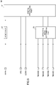
- FIG. 5 is a diagram showing a configuration of a conventional integrated circuit 50.
- the conventional integrated circuit 50 shown in FIG. 5 is, for example, an integrated circuit that performs predetermined processes (for example, amplification, AD conversion, etc.) on a sensor signal output from a sensor.
- the integrated circuit 50 has multiple modes of operation. These multiple operation modes include operation modes for testing the integrated circuit 50.
- the operation mode, in which the integrated circuit 50 operates, can be switched from the outside.
- the integrated circuit 50 includes a first power supply terminal VDD 50, a second power supply terminal VRG, four operation mode signal input terminals TMODE 0 to TMODE 3, a reset signal input terminal RSTB, a reset part 52, an operation mode determining part 53, and a digital processing part 54.
- a first power supply voltage (for example, 5.0 V) for operating the integrated circuit 50 is input to the first power supply terminal VDD 50.
- a second power supply voltage (for example, 1.8 V) for operating the integrated circuit 50 is input to the second power supply terminal VRG.
- An operation mode signal is input to each of the four operation mode signal input terminals TMODE 0 to TMODE 3. Each operation mode signal is set to "0" or "1.”
- An external reset signal RSTB is input to the reset signal input terminal RSTB. When an external reset signal RSTB is input via the reset signal input terminal RSTB, the reset part 52 restarts the digital processing part 54.
- the operation mode determining part 53 determines the operation mode to apply to the operation of the integrated circuit 50.
- the operation mode determining part 53 reports the determined operation mode to the digital processing part 54.
- the operation mode determining part 53 can switch between the 16 operation modes of the digital processing part 54 by using four operation mode signals.
- the integrated circuit 50 is provided with four operation mode signal input terminals TMODE 0 to TMODE 3 for operation-mode switching.
- an integrated circuit includes: a power supply terminal configured to receive a power supply voltage as input; a power supply voltage detection part configured to output a power supply voltage detection signal in accordance with the state of the power supply voltage as input to the power supply terminal; an operation mode signal input terminal configured to receive an operation mode signal as input; and an operation mode determining part configured to determine an operation mode based on the operation mode signal and the power supply voltage detection signal.
- more operation modes can be switched from the outside without increasing the number of input terminals for operation-mode switching.
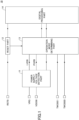
- FIG. 1 is a diagram showing a configuration of an integrated circuit 10 according to one embodiment.
- the integrated circuit 10 shown in FIG. 1 is, for example, an integrated circuit that performs predetermined processes (for example, amplification, AD conversion, etc.) on a sensor signal that is output from a sensor.
- the integrated circuit 10 has multiple modes of operation. These multiple operation modes include operation modes for testing the integrated circuit 10.
- the operation mode, in which the integrated circuit 10 operates, can be switched from the outside.
- the integrated circuit 10 includes a first power supply terminal VDD 50, a second power supply terminal VRG, a first operation mode signal input terminal TMODE 1, a second operation mode signal input terminal TMODE 0, a reset signal input terminal RSTB, a power supply voltage detection part 11, a reset part 12, an operation mode determining part 13, and a digital processing part 14.
- a first power supply voltage (for example, 5.0 V) for operating the integrated circuit 10 is input to the first power supply terminal VDD 50.
- a second power supply voltage (for example, 1.8 V) for operating the integrated circuit 10 is input to the second power supply terminal VRG.
- a first operation mode signal is input to the first operation mode signal input terminal TMODE 1.
- a second operation mode signal is input to the second operation mode signal input terminal TMODE 0.
- the first operation mode signal and the second operation mode signal are set to "0" or "1.”
- An external reset signal RSTB is input to the reset signal input terminal RSTB.
- the power supply voltage detection part 11 detects the first power supply voltage (5.0 V) as input to the first power supply terminal VDD 50, and outputs a first voltage detection signal LVDB, according to the state of the first power supply voltage (5.0 V) as input. To be more specific, the power supply voltage detection part 11 outputs a first power supply voltage detection signal LVDB that becomes "0 (OFF)" when the first power supply voltage (5.0 V) is not input, and becomes “1 (ON)” when the first power supply voltage (5.0 V) is input.
- the power supply voltage detection part 11 detects the second power supply voltage (1.8 V) as input to the second power supply terminal VRG, and outputs a power supply voltage detection signal PORB in accordance with the state of the second power supply voltage (1.8 V) as input. To be more specific, the power supply voltage detection part 11 outputs a second power supply voltage detection signal PORB that becomes “0 (OFF) " when the second power supply voltage (1.8 V) is not input, and becomes “1 (ON)" when the second power supply voltage (1.8 V) is input.
- the "power supply voltage detection part” when the voltage input to the first power supply terminal VDD 50 is compared with a reference voltage by using a comparator and the input voltage reaches a predetermined voltage, the "power supply voltage detection part” outputs the first power supply voltage detection signal LVDB that is "1 (ON).” Also, when the voltage input to the second power supply terminal VRG is compared with a reference voltage by using a comparator and the input voltage reaches a predetermined voltage, the “power supply voltage detection part” outputs the second power supply voltage detection signal PORB that is "1 (ON).” However, as long as the “power supply voltage detection part” can output the first power supply detection signal LVDB and the power supply voltage detection signal PORB of "1" when the first power supply voltage (5.0 V) and the second power supply voltage (1.8 V) are input, the “power supply voltage detection part” may have any configuration and may be configured as, for example, a comparator, an inverter, an amplifier, and the like.
- the reset part 12 restarts the digital processing part 14 when the external reset signal RSTB is input via the reset signal input terminal RSTB.
- the operation mode determining part 13 determines the operation mode to apply to the operation of the integrated circuit 10 based on the first power supply voltage detection signal LVDB, the second power supply voltage detection signal PORB, the first operation mode signal, and the second operation mode signal. The operation mode determining part 13 then reports the determined operation mode to the digital processing part 14.
- the operation mode determining part 13 determines the operation mode that corresponds to the combination of: the value of the first operation mode signal and the value of the second operation mode signal as of when the first power supply voltage detection signal LVDB is switched from “OFF” to “ON”; and the value of the first operation mode signal and the value of the second operation mode signal as of when the second power supply voltage detection signal PORB is switched from “OFF” to “ON,” as the operation mode to apply to the operation of the integrated circuit 10.
- FIG. 2 is a diagram showing an example of a decision table included in the integrated circuit 10 according to one embodiment.
- the integrated circuit 10 supports 16 operation modes (operation mode 1 to operation mode 16).
- the 16 operation modes are, for example, four operation modes, namely a normal operation mode, a test mode 1, a test mode 2, and a test mode 4, where each operation mode is available in four combinations of an operation setting 1 and an operation setting 2.
- the test modes include, for example, a burn-in test mode, a test mode that does not load the NVMs related to the reliability test, a test mode that does not load all the NVMs, a scan test mode, and so forth.
- the operation settings include, for example, whether or not an input filter for I2C (Inter-Integrated Circuit) is provided, whether or not the threshold is changed, and so forth.
- I2C Inter-Integrated Circuit
- each of the 16 operation modes the integrated circuit 10 supports is associated with a combination of four signal values that are input to the integrated circuit 10, serving as a determination condition for determining the operation mode.
- the four signal values input to the integrated circuit 10 refer to: the value of the first operation mode signal and the value of the second operation mode signal as of when the first power supply voltage detection signal LVDB is switched from “0" to "1"; and the value of the first operation mode signal and the value of the second operation mode signal as of when the second power supply voltage detection signal PORB is switched from “0" to "1.”
- TMODE 1 means the value of the first operation mode signal that is input from the first operation mode signal input terminal TMODE 1.
- TMODE 0 means the value of the second operation mode signal that is input from the second operation mode signal input terminal TMODE 0.
- the operation mode determining part 13 selects the operation mode that corresponds to the combination of four signal values input to the integrated circuit 10, from the 16 operation modes for the integrated circuit 10, as the operation mode to apply to the operation of the integrated circuit.
- the operation mode determining part 13 determines "operation mode 1" as the operation mode to apply to the operation of the integrated circuit 10, based on the decision table shown in FIG. 2 .
- FIG. 3 is a diagram showing examples of operation timings of the integrated circuit 10 according to one embodiment.
- the power supply voltage detection part 11 switches the first power supply voltage detection signal LVDB from "0" to "1" (timing t2) .
- the operation mode determining part 13 latches the value of the first operation mode signal that is input from the first operation mode signal input terminal TMODE 1, and the value of the second operation mode signal that is input from the second operation mode signal input terminal TMODE 0.
- the power supply voltage detection part 11 switches the second power supply voltage detection signal PORB from "0" to "1" (timing t5).
- the operation mode determining part 13 latches the value of the first operation mode signal that is input from the first operation mode signal input terminal TMODE 1 and the value of the second operation mode signal that is input from the second operation mode signal input terminal TMODE 0.
- the operation mode determining part 13 determines the operation mode that corresponds to the combination of: the value of the first operation mode signal and the value of the second operation mode signal latched at timing t2; and the value of the first operation mode signal and the value of the second operation mode signal latched at timing t5, as the operation mode to apply to the operation of the integrated circuit 10.
- the operation mode determining part 13 determines "operation mode 1" as the operation mode to apply to the operation of the integrated circuit 10, based on the decision table shown in FIG. 2 .
- the operation mode determining part 13 reports the determined operation mode to the digital processing part 14.
- the integrated circuit 10 operates in the operation mode determined by the operation mode determining part 13.
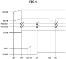
- FIG. 4 is a diagram showing other examples of operation timings of the integrated circuit 10 according to one embodiment.
- the power supply voltage detection part 11 switches the first power supply voltage detection signal LVDB from "0" to "1" (timing t22).
- the operation mode determining part 13 latches the value of the first operation mode signal that is input from the first operation mode signal input terminal TMODE 1, and the value of the second operation mode signal that is input from the second operation mode signal input terminal TMODE 0.
- the power supply voltage detection part 11 switches the second power supply voltage detection signal PORB from "0" to "1" (timing t25).
- the operation mode determining part 13 latches the value of the first operation mode signal that is input from the first operation mode signal input terminal TMODE 1 and the value of the second operation mode signal that is input from the second operation mode signal input terminal TMODE 0.
- the operation mode determining part 13 determines the operation mode that corresponds to the combination of: the value of the first operation mode signal and the value of the second operation mode signal latched at timing t22; and the value of the first operation mode signal and the value of the second operation mode signal latched at timing t25, as the operation mode to apply to the operation of the integrated circuit 10.
- the operation mode determining part 13 determines "operation mode 1" as the operation mode to apply to the operation of the integrated circuit 10, based on the decision table shown in FIG. 2 .
- the operation mode determining part 13 reports the determined operation mode to the digital processing part 14.
- the integrated circuit 10 operates in the operation mode determined by the operation mode determining part 13.
- the integrated circuit 10 includes a power supply terminal that receives a power supply voltage as input, a power supply voltage detection part 11 that outputs a power supply voltage detection signal in accordance with the state of the power supply voltage as input to the power supply terminal, an operation mode signal input terminal that receives an operation mode signal as input, and an operation mode determining part 13 that determines the operation mode based on the operation mode signal and the power supply voltage detection signal.
- the integrated circuit 10 can switch, from the outside, between operation modes that match in number the combinations of the value of the operation mode signal and the value of the power supply voltage detection signal.
- a power supply terminal is provided in all integrated circuits, and therefore can be used without increasing the number of input terminals. Therefore, according to the integrated circuit 10 of one embodiment, more operation modes can be switched from the outside without increasing the number of input terminals for operation-mode switching.
- the integrated circuit 10 includes: a first power supply terminal VDD 50 that receives a first power supply voltage (5.0 V) as input; a second power supply terminal VRG that receives a second power supply voltage (1.8 V) as input; a first operation mode signal input terminal TMODE 1 that receives a first operation mode signal as input; and a second operation mode signal input terminal TMODE 0 that receives a second operation mode signal as input.
- the power supply voltage detection part 11 outputs a first power supply voltage detection signal LVDB in accordance with the state of the first power supply voltage (5.0 V) as input, and outputs a second power supply voltage detection signal PORB in accordance with the state of the second power supply voltage (1.8 V) as input.
- the operation mode determining part 13 determines the operation mode based on the first power supply voltage detection signal LVDB, the second power supply voltage detection signal PORB, the first operation mode signal, and the second operation mode signal.
- the integrated circuit 10 can switch, from the outside, between operation modes that match in number the combinations (that is, 16 combinations) of the first power supply voltage detection signal LVDB, the second power supply voltage detection signal PORB, the first operation mode signal, and the second operation mode signal. Therefore, according to the integrated circuit 10 of one embodiment, more operation modes can be switched from the outside, without increasing the number of input terminals for operation-mode switching.
- the operation mode determining part 13 determines the operation mode that corresponds to the combination of: the value of the first operation mode signal and the value of the second operation mode signal as of when the first power supply voltage detection signal LVDB is switched from “OFF” to “ON”; and the value of the first operation mode signal and the value of the second operation mode signal as of when the second power supply voltage detection signal PORB is switched from “OFF” to “ON,” as the operation mode.
- the integrated circuit 10 can utilize the timing at which the first power supply voltage (5.0 V) is input and the timing at which the second power supply voltage (1.8 V) is input, to allow the value of the first operation mode signal and the value of the second operation mode signal to have different meanings. That is, the integrated circuit 10 according to one embodiment acquires the value of the first operation mode signal and the value of the second operation mode signal at two respective timings, so that the integrated circuit 10 can double the number of combinations of the value of the first operation mode signal and the value of the second operation mode signal (the number of operation modes subject to switching) without increasing the number of input terminals for operation-mode switching.
- the integrated circuit 10 is applicable to, for example, an AFE (Analog Front End) for connecting between a plurality of sensors (for example, a plurality of strain sensors for detecting the load applied to an object) and an MCU (Micro Control Unit).
- AFE Analog Front End
- MCU Micro Control Unit
- the integrated circuit 10 functions as the AFE, and is composed of a multiplexer that selects any one of a plurality of sensor signals output from a plurality of sensors, an amplifier that amplifies the sensor signal selected by the multiplexer; an AD converter that converts the sensor signal amplified by the amplifier from an analog signal to a digital signal; a digital processing circuit (equivalent to the digital processing part 14) that performs predetermined digital processing (including, for example, digital filtering, data transmission to the MCU via I2C communication, etc.) on the sensor signal (digital signal) output from the AD converter.
- predetermined digital processing including, for example, digital filtering, data transmission to the MCU via I2C communication, etc.
- the operation mode determining part 13 may determine the operation mode corresponding to a combination of: the value of the first operation mode signal and the value of the second operation mode signal as of when the first power supply voltage detection signal LVDB is switched from “OFF” to “ON”; the value of the first operation mode signal and the value of the second operation mode signal as of when the second power supply voltage detection signal PORB is switched from “OFF” to “ON”; and the order in which the first power supply voltage detection signal LVDB and the second power supply voltage detection signal PORB are switched from “OFF” to "ON,” as the operation mode.
- the integrated circuit 10 can switch, from the outside, between operation modes that match in number the combinations (that is, 32 combinations) of the first power supply voltage detection signal LVDB, the second power supply voltage detection signal PORB, the first operation mode signal, the second operation mode signal, and the order in which the first power supply voltage detection signal LVDB and the second power supply voltage detection signal PORB are switched from “OFF" to "ON.”
- two input terminals are provided on an integrated circuit for receiving operation mode signals as input
- two power supply terminals are provided on the integrated circuit
- an external reset terminal in addition to power supply terminals, for operation-mode switching
- an external reset terminal may be used instead of power supply terminals for operation-mode switching.
Landscapes
- Engineering & Computer Science (AREA)
- General Engineering & Computer Science (AREA)
- Physics & Mathematics (AREA)
- General Physics & Mathematics (AREA)
- Semiconductor Integrated Circuits (AREA)
- Tests Of Electronic Circuits (AREA)
- Electronic Switches (AREA)
Abstract
Description
- The present invention relates to an integrated circuit.
-
Patent Document 1 below discloses a technique for outputting one of a signal that is output from a boundary scan register and a signal that is output from a scan flip-flop circuit, from a multiplexer, depending on the value of a mode signal that is input to the multiplexer, in an output buffer provided in a semiconductor integrated circuit. - Patent Document 1: Unexamined
Japanese Patent Application Publication No. 2004-260093 - However, according to the technique of
Patent Document 1, there is only one mode-signal input terminal, so that it is only possible to switch between two operation modes. Consequently, with the above conventional technique, in order to switch more operation modes from the outside, it is then necessary to increase the number of input terminals for operation-mode switching. For example, given a conventional integrated circuit, in order to switch between 16 operation modes from the outside, it is necessary to provide at least four input terminals for operation-mode switching. - For example,
FIG. 5 is a diagram showing a configuration of a conventional integrated circuit 50. The conventional integrated circuit 50 shown inFIG. 5 is, for example, an integrated circuit that performs predetermined processes (for example, amplification, AD conversion, etc.) on a sensor signal output from a sensor. The integrated circuit 50 has multiple modes of operation. These multiple operation modes include operation modes for testing the integrated circuit 50. The operation mode, in which the integrated circuit 50 operates, can be switched from the outside. - As shown in
FIG. 5 , the integrated circuit 50 includes a first power supply terminal VDD 50, a second power supply terminal VRG, four operation mode signal input terminals TMODE 0 to TMODE 3, a reset signal input terminal RSTB, areset part 52, an operationmode determining part 53, and adigital processing part 54. - A first power supply voltage (for example, 5.0 V) for operating the integrated circuit 50 is input to the first power supply terminal VDD 50. A second power supply voltage (for example, 1.8 V) for operating the integrated circuit 50 is input to the second power supply terminal VRG. An operation mode signal is input to each of the four operation mode signal input terminals TMODE 0 to TMODE 3. Each operation mode signal is set to "0" or "1." An external reset signal RSTB is input to the reset signal input terminal RSTB. When an external reset signal RSTB is input via the reset signal input terminal RSTB, the
reset part 52 restarts thedigital processing part 54. - Based on the four operation mode signals input from the four operation mode signal input terminals TMODE 0 to TMODE 3, the operation
mode determining part 53 determines the operation mode to apply to the operation of the integrated circuit 50. The operationmode determining part 53 then reports the determined operation mode to thedigital processing part 54. As a result of this, the operationmode determining part 53 can switch between the 16 operation modes of thedigital processing part 54 by using four operation mode signals. For this reason, the integrated circuit 50 is provided with four operation mode signal input terminals TMODE 0 to TMODE 3 for operation-mode switching. - According to one embodiment of the present disclosure, an integrated circuit includes: a power supply terminal configured to receive a power supply voltage as input; a power supply voltage detection part configured to output a power supply voltage detection signal in accordance with the state of the power supply voltage as input to the power supply terminal; an operation mode signal input terminal configured to receive an operation mode signal as input; and an operation mode determining part configured to determine an operation mode based on the operation mode signal and the power supply voltage detection signal.
- According to the above integrated circuit of one embodiment, more operation modes can be switched from the outside without increasing the number of input terminals for operation-mode switching.
-
-
FIG. 1 is a diagram showing a configuration of an integrated circuit according to one embodiment; -
FIG. 2 is a diagram showing an example of a decision table included in the integrated circuit according to one embodiment; -
FIG. 3 is a diagram showing examples of operation timings of the integrated circuit according to one embodiment; -
FIG. 4 is a diagram showing other examples of operation timings of the integrated circuit according to one embodiment; and -
FIG. 5 is a diagram showing a configuration of a conventional integrated circuit. - An embodiment will be described below with reference to the accompanying drawings.
-
FIG. 1 is a diagram showing a configuration of an integratedcircuit 10 according to one embodiment. Theintegrated circuit 10 shown inFIG. 1 is, for example, an integrated circuit that performs predetermined processes (for example, amplification, AD conversion, etc.) on a sensor signal that is output from a sensor. Theintegrated circuit 10 has multiple modes of operation. These multiple operation modes include operation modes for testing theintegrated circuit 10. The operation mode, in which theintegrated circuit 10 operates, can be switched from the outside. - As shown in
FIG. 1 , theintegrated circuit 10 includes a first power supply terminal VDD 50, a second power supply terminal VRG, a first operation mode signalinput terminal TMODE 1, a second operation mode signalinput terminal TMODE 0, a reset signal input terminal RSTB, a power supplyvoltage detection part 11, areset part 12, an operationmode determining part 13, and adigital processing part 14. - A first power supply voltage (for example, 5.0 V) for operating the
integrated circuit 10 is input to the first power supply terminal VDD 50. A second power supply voltage (for example, 1.8 V) for operating the integratedcircuit 10 is input to the second power supply terminal VRG. A first operation mode signal is input to the first operation mode signalinput terminal TMODE 1. A second operation mode signal is input to the second operation mode signalinput terminal TMODE 0. The first operation mode signal and the second operation mode signal are set to "0" or "1." An external reset signal RSTB is input to the reset signal input terminal RSTB. - The power supply
voltage detection part 11 detects the first power supply voltage (5.0 V) as input to the first power supply terminal VDD 50, and outputs a first voltage detection signal LVDB, according to the state of the first power supply voltage (5.0 V) as input. To be more specific, the power supplyvoltage detection part 11 outputs a first power supply voltage detection signal LVDB that becomes "0 (OFF)" when the first power supply voltage (5.0 V) is not input, and becomes "1 (ON)" when the first power supply voltage (5.0 V) is input. - Also, the power supply
voltage detection part 11 detects the second power supply voltage (1.8 V) as input to the second power supply terminal VRG, and outputs a power supply voltage detection signal PORB in accordance with the state of the second power supply voltage (1.8 V) as input. To be more specific, the power supplyvoltage detection part 11 outputs a second power supply voltage detection signal PORB that becomes "0 (OFF) " when the second power supply voltage (1.8 V) is not input, and becomes "1 (ON)" when the second power supply voltage (1.8 V) is input. - To be more specific, when the voltage input to the first power supply terminal VDD 50 is compared with a reference voltage by using a comparator and the input voltage reaches a predetermined voltage, the "power supply voltage detection part" outputs the first power supply voltage detection signal LVDB that is "1 (ON)." Also, when the voltage input to the second power supply terminal VRG is compared with a reference voltage by using a comparator and the input voltage reaches a predetermined voltage, the "power supply voltage detection part" outputs the second power supply voltage detection signal PORB that is "1 (ON)." However, as long as the "power supply voltage detection part" can output the first power supply detection signal LVDB and the power supply voltage detection signal PORB of "1" when the first power supply voltage (5.0 V) and the second power supply voltage (1.8 V) are input, the "power supply voltage detection part" may have any configuration and may be configured as, for example, a comparator, an inverter, an amplifier, and the like.
- The
reset part 12 restarts thedigital processing part 14 when the external reset signal RSTB is input via the reset signal input terminal RSTB. - The operation
mode determining part 13 determines the operation mode to apply to the operation of theintegrated circuit 10 based on the first power supply voltage detection signal LVDB, the second power supply voltage detection signal PORB, the first operation mode signal, and the second operation mode signal. The operationmode determining part 13 then reports the determined operation mode to thedigital processing part 14. - To be more specific, the operation
mode determining part 13 determines the operation mode that corresponds to the combination of: the value of the first operation mode signal and the value of the second operation mode signal as of when the first power supply voltage detection signal LVDB is switched from "OFF" to "ON"; and the value of the first operation mode signal and the value of the second operation mode signal as of when the second power supply voltage detection signal PORB is switched from "OFF" to "ON," as the operation mode to apply to the operation of the integratedcircuit 10. -
FIG. 2 is a diagram showing an example of a decision table included in the integratedcircuit 10 according to one embodiment. As shown inFIG. 2 , theintegrated circuit 10 according to one embodiment supports 16 operation modes (operation mode 1 to operation mode 16). The 16 operation modes are, for example, four operation modes, namely a normal operation mode, atest mode 1, atest mode 2, and atest mode 4, where each operation mode is available in four combinations of an operation setting 1 and an operation setting 2. The test modes include, for example, a burn-in test mode, a test mode that does not load the NVMs related to the reliability test, a test mode that does not load all the NVMs, a scan test mode, and so forth. Also, the operation settings include, for example, whether or not an input filter for I2C (Inter-Integrated Circuit) is provided, whether or not the threshold is changed, and so forth. - In the decision table shown in
FIG. 2 , each of the 16 operation modes theintegrated circuit 10 supports is associated with a combination of four signal values that are input to theintegrated circuit 10, serving as a determination condition for determining the operation mode. - The four signal values input to the
integrated circuit 10 refer to: the value of the first operation mode signal and the value of the second operation mode signal as of when the first power supply voltage detection signal LVDB is switched from "0" to "1"; and the value of the first operation mode signal and the value of the second operation mode signal as of when the second power supply voltage detection signal PORB is switched from "0" to "1." - Note that, in the decision table shown in
FIG. 2 , "LVDB = 1" indicates when the first power supply voltage detection signal LVDB is switched from "0" to "1." - Also, in the decision table shown in
FIG. 2 , "PORB = 1" indicates when the second power supply voltage detection signal PORB is switched from "0" to "1." - Also, in the decision table shown in
FIG. 2 , "TMODE 1" means the value of the first operation mode signal that is input from the first operation mode signalinput terminal TMODE 1. - Also, in the decision table shown in
FIG. 2 , "TMODE 0" means the value of the second operation mode signal that is input from the second operation mode signalinput terminal TMODE 0. - Based on the decision table shown in
FIG. 2 , the operationmode determining part 13 selects the operation mode that corresponds to the combination of four signal values input to theintegrated circuit 10, from the 16 operation modes for theintegrated circuit 10, as the operation mode to apply to the operation of the integrated circuit. - For example, when the value of the first operation mode signal and the value of the second operation mode signal as of when the first power supply voltage detection signal LVDB is switched from "0" to "1"; and the value of the first operation mode signal and the value of the second operation mode signal as of when the second power supply voltage detection signal PORB is switched from "0" to "1" are all "0," the operation
mode determining part 13 determines "operation mode 1" as the operation mode to apply to the operation of theintegrated circuit 10, based on the decision table shown inFIG. 2 . -
FIG. 3 is a diagram showing examples of operation timings of theintegrated circuit 10 according to one embodiment. - As shown in
FIG. 3 , when a voltage starts being applied to the first power supply terminal VDD 50 (timing t1) and subsequently the voltage value at the first power supply terminal VDD 50 reaches a predetermined voltage, the power supplyvoltage detection part 11 switches the first power supply voltage detection signal LVDB from "0" to "1" (timing t2) . - At this timing, the operation
mode determining part 13 latches the value of the first operation mode signal that is input from the first operation mode signalinput terminal TMODE 1, and the value of the second operation mode signal that is input from the second operation mode signalinput terminal TMODE 0. - Following this, when a voltage starts being applied to the second power supply terminal VRG (timing t3) and subsequently the voltage value at the second power supply terminal VRG reaches a predetermined voltage (timing t4), the power supply
voltage detection part 11 switches the second power supply voltage detection signal PORB from "0" to "1" (timing t5). - At this timing, the operation
mode determining part 13 latches the value of the first operation mode signal that is input from the first operation mode signalinput terminal TMODE 1 and the value of the second operation mode signal that is input from the second operation mode signalinput terminal TMODE 0. - Then, based on the decision table shown in
FIG. 2 , the operationmode determining part 13 determines the operation mode that corresponds to the combination of: the value of the first operation mode signal and the value of the second operation mode signal latched at timing t2; and the value of the first operation mode signal and the value of the second operation mode signal latched at timing t5, as the operation mode to apply to the operation of theintegrated circuit 10. - For example, in the example shown in
FIG. 3 , the value of the first operation mode signal and the value of the second operation mode signal latched at timing t2; and the value of the first operation mode signal and the value of the second operation mode signal latched at timing t5, are all "0." In this case, the operationmode determining part 13 determines "operation mode 1" as the operation mode to apply to the operation of theintegrated circuit 10, based on the decision table shown inFIG. 2 . - Furthermore, the operation
mode determining part 13 reports the determined operation mode to thedigital processing part 14. As a result of this, theintegrated circuit 10 operates in the operation mode determined by the operationmode determining part 13. -
FIG. 4 is a diagram showing other examples of operation timings of theintegrated circuit 10 according to one embodiment. - As shown in
FIG. 4 , when a voltage starts being applied to the first power supply terminal VDD 50 (timing t21) and subsequently the voltage value at the first power supply terminal VDD 50 reaches a predetermined voltage, the power supplyvoltage detection part 11 switches the first power supply voltage detection signal LVDB from "0" to "1" (timing t22). - At this timing, the operation
mode determining part 13 latches the value of the first operation mode signal that is input from the first operation mode signalinput terminal TMODE 1, and the value of the second operation mode signal that is input from the second operation mode signalinput terminal TMODE 0. - Following this, when a voltage starts being applied to the second power supply terminal VRG (timing t23) and subsequently the voltage value at the second power supply terminal VRG reaches a predetermined voltage (timing t24), the power supply
voltage detection part 11 switches the second power supply voltage detection signal PORB from "0" to "1" (timing t25). - Subsequently, when the external reset signal RSTB that is input from the reset signal input terminal RSTB switches from "1" to "0" (timing t26), and, furthermore, the external reset signal RSTB switches from "0" to "1" (timing t27), at this timing, the operation
mode determining part 13 latches the value of the first operation mode signal that is input from the first operation mode signalinput terminal TMODE 1 and the value of the second operation mode signal that is input from the second operation mode signalinput terminal TMODE 0. - Then, based on the decision table shown in
FIG. 2 , the operationmode determining part 13 determines the operation mode that corresponds to the combination of: the value of the first operation mode signal and the value of the second operation mode signal latched at timing t22; and the value of the first operation mode signal and the value of the second operation mode signal latched at timing t25, as the operation mode to apply to the operation of theintegrated circuit 10. - For example, in the example shown in
FIG. 4 , the value of the first operation mode signal and the value of the second operation mode signal latched at timing t22; and the value of the first operation mode signal and the value of the second operation mode signal latched at timing t27, are all "0." In this case, the operationmode determining part 13 determines "operation mode 1" as the operation mode to apply to the operation of theintegrated circuit 10, based on the decision table shown inFIG. 2 . - Furthermore, the operation
mode determining part 13 reports the determined operation mode to thedigital processing part 14. As a result of this, theintegrated circuit 10 operates in the operation mode determined by the operationmode determining part 13. - As described above, the
integrated circuit 10 according to one embodiment includes a power supply terminal that receives a power supply voltage as input, a power supplyvoltage detection part 11 that outputs a power supply voltage detection signal in accordance with the state of the power supply voltage as input to the power supply terminal, an operation mode signal input terminal that receives an operation mode signal as input, and an operationmode determining part 13 that determines the operation mode based on the operation mode signal and the power supply voltage detection signal. - By this means, the
integrated circuit 10 according to one embodiment can switch, from the outside, between operation modes that match in number the combinations of the value of the operation mode signal and the value of the power supply voltage detection signal. A power supply terminal is provided in all integrated circuits, and therefore can be used without increasing the number of input terminals. Therefore, according to theintegrated circuit 10 of one embodiment, more operation modes can be switched from the outside without increasing the number of input terminals for operation-mode switching. - Also, the
integrated circuit 10 according to one embodiment includes: a first power supply terminal VDD 50 that receives a first power supply voltage (5.0 V) as input; a second power supply terminal VRG that receives a second power supply voltage (1.8 V) as input; a first operation mode signalinput terminal TMODE 1 that receives a first operation mode signal as input; and a second operation mode signalinput terminal TMODE 0 that receives a second operation mode signal as input. The power supplyvoltage detection part 11 outputs a first power supply voltage detection signal LVDB in accordance with the state of the first power supply voltage (5.0 V) as input, and outputs a second power supply voltage detection signal PORB in accordance with the state of the second power supply voltage (1.8 V) as input. The operationmode determining part 13 determines the operation mode based on the first power supply voltage detection signal LVDB, the second power supply voltage detection signal PORB, the first operation mode signal, and the second operation mode signal. - By this means, the
integrated circuit 10 according to one embodiment can switch, from the outside, between operation modes that match in number the combinations (that is, 16 combinations) of the first power supply voltage detection signal LVDB, the second power supply voltage detection signal PORB, the first operation mode signal, and the second operation mode signal. Therefore, according to theintegrated circuit 10 of one embodiment, more operation modes can be switched from the outside, without increasing the number of input terminals for operation-mode switching. - Also, in the
integrated circuit 10 according to one embodiment, the operationmode determining part 13 determines the operation mode that corresponds to the combination of: the value of the first operation mode signal and the value of the second operation mode signal as of when the first power supply voltage detection signal LVDB is switched from "OFF" to "ON"; and the value of the first operation mode signal and the value of the second operation mode signal as of when the second power supply voltage detection signal PORB is switched from "OFF" to "ON," as the operation mode. - By this means, the
integrated circuit 10 according to one embodiment can utilize the timing at which the first power supply voltage (5.0 V) is input and the timing at which the second power supply voltage (1.8 V) is input, to allow the value of the first operation mode signal and the value of the second operation mode signal to have different meanings. That is, theintegrated circuit 10 according to one embodiment acquires the value of the first operation mode signal and the value of the second operation mode signal at two respective timings, so that theintegrated circuit 10 can double the number of combinations of the value of the first operation mode signal and the value of the second operation mode signal (the number of operation modes subject to switching) without increasing the number of input terminals for operation-mode switching. - Note that the
integrated circuit 10 according to one embodiment is applicable to, for example, an AFE (Analog Front End) for connecting between a plurality of sensors (for example, a plurality of strain sensors for detecting the load applied to an object) and an MCU (Micro Control Unit). In this case, theintegrated circuit 10 functions as the AFE, and is composed of a multiplexer that selects any one of a plurality of sensor signals output from a plurality of sensors, an amplifier that amplifies the sensor signal selected by the multiplexer; an AD converter that converts the sensor signal amplified by the amplifier from an analog signal to a digital signal; a digital processing circuit (equivalent to the digital processing part 14) that performs predetermined digital processing (including, for example, digital filtering, data transmission to the MCU via I2C communication, etc.) on the sensor signal (digital signal) output from the AD converter. - Although one embodiment of the present invention has been described in detail above, the present invention is not limited to this embodiment, and a variety of alterations and changes can be made within the scope of the claims recited herein.
- For example, in the
integrated circuit 10 according to one embodiment, the operationmode determining part 13 may determine the operation mode corresponding to a combination of: the value of the first operation mode signal and the value of the second operation mode signal as of when the first power supply voltage detection signal LVDB is switched from "OFF" to "ON"; the value of the first operation mode signal and the value of the second operation mode signal as of when the second power supply voltage detection signal PORB is switched from "OFF" to "ON"; and the order in which the first power supply voltage detection signal LVDB and the second power supply voltage detection signal PORB are switched from "OFF" to "ON," as the operation mode. - By this means, the
integrated circuit 10 according to one embodiment can switch, from the outside, between operation modes that match in number the combinations (that is, 32 combinations) of the first power supply voltage detection signal LVDB, the second power supply voltage detection signal PORB, the first operation mode signal, the second operation mode signal, and the order in which the first power supply voltage detection signal LVDB and the second power supply voltage detection signal PORB are switched from "OFF" to "ON." - Also, although, for example, in one embodiment, two input terminals are provided on an integrated circuit for receiving operation mode signals as input, this is by no means a limitation, and, in the event the integrated circuit is provided with three or more input terminals for receiving operation mode signals as input, it then becomes possible to switch between a larger number of operation modes, from the outside, by using these three or more input terminals for operation-mode switching.
- For example, although, in one embodiment, two power supply terminals are provided on the integrated circuit, this is by no means a limitation, and, in the event the integrated circuit is provided with three or more power supply terminals, it then becomes possible to switch between a larger number of operation modes, from the outside, by using these three or more input terminals for operation-mode switching.
- Also, although an example has been described with one embodiment where an external reset terminal is used, in addition to power supply terminals, for operation-mode switching, this is by no means a limitation, and for example, an external reset terminal may be used instead of power supply terminals for operation-mode switching. In this case, again, it is possible to switch between a larger number of operation modes from the outside, without increasing the number of terminals for operation-mode switching.
- This international application is based on and claims priority to
Japanese Patent Application No. 2020-070469, filed on April 9, 2020 -
- 10
- integrated circuit
- 12
- reset part
- 11
- power supply voltage detection part
- 13
- operation mode determining part
- 14
- digital processing part
- RSTB
- reset signal input terminal
-
TMODE 1 - first operation mode signal input terminal
-
TMODE 0 - second operation mode signal input terminal
- VDD 50
- first power supply terminal
- VRG
- second power supply terminal
Claims (7)
- An integrated circuit comprising:a power supply terminal configured to receive a power supply voltage as input;a power supply voltage detection part configured to output a power supply voltage detection signal in accordance with a state of the power supply voltage as input to the power supply terminal;an operation mode signal input terminal configured to receive an operation mode signal as input; andan operation mode determining part configured to determine an operation mode based on the operation mode signal and the power supply voltage detection signal.
- The integrated circuit according to claim 1, further comprising:a first power supply terminal configured to receive a first power supply voltage as input;a second power supply terminal configured to receive a second power supply voltage as input;a first operation mode signal input terminal configured to receive a first operation mode signal as input; anda second operation mode signal input terminal configured to receive a second operation mode signal as input,wherein the power supply voltage detection part outputs a first power supply voltage detection signal in accordance with a state of the first power supply voltage as input and outputs a second power supply voltage detection signal in accordance with a state of the second power supply voltage as input, andwherein the operation mode determining part determines the operation mode based on the first power supply voltage detection signal, the second power supply voltage detection signal, the first operation mode signal, and the second operation mode signal.
- The integrated circuit according to claim 2, wherein the operation mode determining part determines an operation mode that corresponds to a combination of: a value of the first operation mode signal and a value of the second operation mode signal as of when the first power supply voltage detection signal is switched from "OFF" to "ON"; and the value of the first operation mode signal and the value of the second operation mode signal as of when the second power supply voltage detection signal is switched from "OFF" to "ON," as the operation mode.
- The integrated circuit according to claim 3, wherein the operation mode determining part latches the value of the first operation mode signal and the value of the second operation mode signal when the first power supply voltage detection signal is switched from "OFF" to "ON," latches the value of the first operation mode signal and the value of the second operation mode signal when the second power supply voltage detection signal is switched from "OFF" to "ON," and determines an operation mode that corresponds to a combination of the four latched values as the operation mode.
- The integrated circuit according to claim 2, wherein the operation mode determining part determines an operation mode that corresponds to a combination of: the value of the first operation mode signal and the value of the second operation mode signal as of when the first power supply voltage detection signal is switched from "OFF" to "ON"; the value of the first operation mode signal and the value of the second operation mode signal as of when the second power supply voltage detection signal is switched from "OFF" to "ON"; and an order in which the first power supply voltage detection signal and the second power supply voltage detection signal are switched from "OFF" to "ON," as the operation mode.
- The integrated circuit according to claim 2, wherein the operation mode determining part determines an operation mode that corresponds to a combination of: the value of the first operation mode signal and the value of the second operation mode signal as of when the first power supply voltage detection signal is switched from "OFF" to "ON"; and the value of the first operation mode signal and the value of the second operation mode signal as of when an external reset signal is switched after the second power supply voltage detection signal is switched from "OFF" to "ON," as the operation mode.
- An integrated circuit comprising:a reset signal input terminal configured to receive an external reset signal as input;an operation mode signal input terminal configured to receive an operation mode signal as input; andan operation mode determining part configured to determine an operation mode based on the operation mode signal and the external reset signal.
Applications Claiming Priority (2)
| Application Number | Priority Date | Filing Date | Title |
|---|---|---|---|
| JP2020070469A JP7551324B2 (en) | 2020-04-09 | 2020-04-09 | Integrated Circuits |
| PCT/JP2021/013280 WO2021205924A1 (en) | 2020-04-09 | 2021-03-29 | Integrated circuit |
Publications (2)
| Publication Number | Publication Date |
|---|---|
| EP4135033A1 true EP4135033A1 (en) | 2023-02-15 |
| EP4135033A4 EP4135033A4 (en) | 2023-09-13 |
Family
ID=78023051
Family Applications (1)
| Application Number | Title | Priority Date | Filing Date |
|---|---|---|---|
| EP21785344.9A Pending EP4135033A4 (en) | 2020-04-09 | 2021-03-29 | INTEGRATED CIRCUIT |
Country Status (4)
| Country | Link |
|---|---|
| EP (1) | EP4135033A4 (en) |
| JP (2) | JP7551324B2 (en) |
| CN (1) | CN115335995B (en) |
| WO (1) | WO2021205924A1 (en) |
Family Cites Families (16)
| Publication number | Priority date | Publication date | Assignee | Title |
|---|---|---|---|---|
| JP2639319B2 (en) * | 1993-09-22 | 1997-08-13 | 日本電気株式会社 | Semiconductor device |
| JPH09204412A (en) * | 1996-01-24 | 1997-08-05 | Kawasaki Steel Corp | Microcomputer |
| US5822246A (en) * | 1996-09-30 | 1998-10-13 | Intel Corporation | Method and apparatus for detecting the voltage on the VCC pin |
| JP2001228220A (en) | 2000-02-21 | 2001-08-24 | Matsushita Electric Ind Co Ltd | Test circuit for semiconductor device |
| JP2004045090A (en) | 2002-07-09 | 2004-02-12 | Renesas Technology Corp | Semiconductor integrated circuit |
| JP3842228B2 (en) | 2003-02-27 | 2006-11-08 | Necエレクトロニクス株式会社 | Semiconductor integrated circuit device, design automation device and method, and program |
| JP4660115B2 (en) * | 2004-05-19 | 2011-03-30 | パナソニック株式会社 | Test mode setting circuit |
| JP2006029948A (en) | 2004-07-15 | 2006-02-02 | Sony Corp | Semiconductor integrated circuit test mode setting method and semiconductor integrated circuit |
| JP4677790B2 (en) * | 2005-01-18 | 2011-04-27 | 富士電機システムズ株式会社 | Switching power supply intermittent protection circuit |
| JP2006332456A (en) | 2005-05-27 | 2006-12-07 | Fujitsu Ltd | Semiconductor device and test mode setting method |
| JP4967395B2 (en) | 2006-03-22 | 2012-07-04 | 富士電機株式会社 | Semiconductor integrated circuit |
| JP4755123B2 (en) * | 2007-02-19 | 2011-08-24 | ルネサスエレクトロニクス株式会社 | Operation mode control circuit for information processing apparatus and information processing apparatus |
| JP5620718B2 (en) | 2010-06-07 | 2014-11-05 | スパンションエルエルシー | Integrated circuit device having voltage regulator |
| JP2013190256A (en) | 2012-03-13 | 2013-09-26 | Ricoh Co Ltd | Semiconductor integrated circuit and test mode setting method for the same |
| JP6040868B2 (en) * | 2013-06-04 | 2016-12-07 | 株式会社デンソー | Microcomputer |
| JP6845205B2 (en) | 2018-10-31 | 2021-03-17 | Tdk株式会社 | Soft magnetic alloy strips and magnetic parts |
-
2020
- 2020-04-09 JP JP2020070469A patent/JP7551324B2/en active Active
-
2021
- 2021-03-29 EP EP21785344.9A patent/EP4135033A4/en active Pending
- 2021-03-29 WO PCT/JP2021/013280 patent/WO2021205924A1/en not_active Ceased
- 2021-03-29 CN CN202180024699.3A patent/CN115335995B/en active Active
-
2024
- 2024-09-03 JP JP2024151191A patent/JP7823993B2/en active Active
Also Published As
| Publication number | Publication date |
|---|---|
| JP2021168328A (en) | 2021-10-21 |
| CN115335995B (en) | 2026-03-17 |
| WO2021205924A1 (en) | 2021-10-14 |
| JP2024161183A (en) | 2024-11-15 |
| CN115335995A (en) | 2022-11-11 |
| EP4135033A4 (en) | 2023-09-13 |
| JP7551324B2 (en) | 2024-09-17 |
| JP7823993B2 (en) | 2026-03-04 |
Similar Documents
| Publication | Publication Date | Title |
|---|---|---|
| US7126515B1 (en) | Selectable real time sample triggering for a plurality of inputs of an analog-to-digital converter | |
| US6137432A (en) | Low-power column parallel ADC in CMOS image sensors | |
| EP3606043B1 (en) | Analog-to-digital converter circuit, image sensor, and analog-to-digital conversion method | |
| US10216238B2 (en) | Power-on reset circuit | |
| US20080012604A1 (en) | Low-voltage detection circuit | |
| US20100103006A1 (en) | Adc test circuit and semiconductor device | |
| TWI407129B (en) | Adjustable voltage comparing circuit and adjustable voltage examining module | |
| CN1722561B (en) | Battery protection circuit | |
| JP2010154441A (en) | Apparatus and method for diagnosing fault of a/d input circuit | |
| US20190212715A1 (en) | Signal processing device and control method of signal processing device | |
| JP7823993B2 (en) | Integrated Circuits | |
| JP2008131670A (en) | Battery voltage monitoring device | |
| JP2015167278A (en) | A / D converter output switching method and A / D converter | |
| CN211318719U (en) | Magnet detection system | |
| JP2001035335A (en) | Relay failure detecting device | |
| TW202220388A (en) | Pipeline analog to digital converter and timing adjustment method | |
| CN110572225B (en) | Receiver direct current offset monitoring system, method, electronic device and storage medium | |
| EP4135017B1 (en) | Integrated circuit | |
| JP2000209090A (en) | A / D converter | |
| CN112422129B (en) | Direct X-ray detector CMOS reading circuit and control method | |
| US10447266B2 (en) | Low power energy detector | |
| US6693570B2 (en) | Digital-to-analog conversion circuitry incorporating a simplified testing circuit | |
| US9870331B2 (en) | Interface circuit | |
| US20190229744A1 (en) | Peak/bottom detection circuit, a/d converter, and integrated circuit | |
| JP3298908B2 (en) | Analog-to-digital converter |
Legal Events
| Date | Code | Title | Description |
|---|---|---|---|
| STAA | Information on the status of an ep patent application or granted ep patent |
Free format text: STATUS: THE INTERNATIONAL PUBLICATION HAS BEEN MADE |
|
| PUAI | Public reference made under article 153(3) epc to a published international application that has entered the european phase |
Free format text: ORIGINAL CODE: 0009012 |
|
| STAA | Information on the status of an ep patent application or granted ep patent |
Free format text: STATUS: REQUEST FOR EXAMINATION WAS MADE |
|
| 17P | Request for examination filed |
Effective date: 20221005 |
|
| AK | Designated contracting states |
Kind code of ref document: A1 Designated state(s): AL AT BE BG CH CY CZ DE DK EE ES FI FR GB GR HR HU IE IS IT LI LT LU LV MC MK MT NL NO PL PT RO RS SE SI SK SM TR |
|
| DAV | Request for validation of the european patent (deleted) | ||
| DAX | Request for extension of the european patent (deleted) | ||
| A4 | Supplementary search report drawn up and despatched |
Effective date: 20230814 |
|
| RIC1 | Information provided on ipc code assigned before grant |
Ipc: H03K 17/22 20060101ALI20230808BHEP Ipc: H03K 17/00 20060101ALI20230808BHEP Ipc: G01R 31/3185 20060101ALI20230808BHEP Ipc: G01R 31/28 20060101ALI20230808BHEP Ipc: H01L 27/04 20060101AFI20230808BHEP |