EP4133330B1 - Dispositif de contrôle de la réflectivité infrarouge - Google Patents
Dispositif de contrôle de la réflectivité infrarouge Download PDFInfo
- Publication number
- EP4133330B1 EP4133330B1 EP21718966.1A EP21718966A EP4133330B1 EP 4133330 B1 EP4133330 B1 EP 4133330B1 EP 21718966 A EP21718966 A EP 21718966A EP 4133330 B1 EP4133330 B1 EP 4133330B1
- Authority
- EP
- European Patent Office
- Prior art keywords
- control device
- infrared
- electrodes
- infrared reflectivity
- reflectivity control
- Prior art date
- Legal status (The legal status is an assumption and is not a legal conclusion. Google has not performed a legal analysis and makes no representation as to the accuracy of the status listed.)
- Active
Links
Images


Classifications
-
- G—PHYSICS
- G02—OPTICS
- G02F—OPTICAL DEVICES OR ARRANGEMENTS FOR THE CONTROL OF LIGHT BY MODIFICATION OF THE OPTICAL PROPERTIES OF THE MEDIA OF THE ELEMENTS INVOLVED THEREIN; NON-LINEAR OPTICS; FREQUENCY-CHANGING OF LIGHT; OPTICAL LOGIC ELEMENTS; OPTICAL ANALOGUE/DIGITAL CONVERTERS
- G02F1/00—Devices or arrangements for the control of the intensity, colour, phase, polarisation or direction of light arriving from an independent light source, e.g. switching, gating or modulating; Non-linear optics
- G02F1/01—Devices or arrangements for the control of the intensity, colour, phase, polarisation or direction of light arriving from an independent light source, e.g. switching, gating or modulating; Non-linear optics for the control of the intensity, phase, polarisation or colour
- G02F1/165—Devices or arrangements for the control of the intensity, colour, phase, polarisation or direction of light arriving from an independent light source, e.g. switching, gating or modulating; Non-linear optics for the control of the intensity, phase, polarisation or colour based on translational movement of particles in a fluid under the influence of an applied field
- G02F1/166—Devices or arrangements for the control of the intensity, colour, phase, polarisation or direction of light arriving from an independent light source, e.g. switching, gating or modulating; Non-linear optics for the control of the intensity, phase, polarisation or colour based on translational movement of particles in a fluid under the influence of an applied field characterised by the electro-optical or magneto-optical effect
- G02F1/167—Devices or arrangements for the control of the intensity, colour, phase, polarisation or direction of light arriving from an independent light source, e.g. switching, gating or modulating; Non-linear optics for the control of the intensity, phase, polarisation or colour based on translational movement of particles in a fluid under the influence of an applied field characterised by the electro-optical or magneto-optical effect by electrophoresis
-
- G—PHYSICS
- G02—OPTICS
- G02F—OPTICAL DEVICES OR ARRANGEMENTS FOR THE CONTROL OF LIGHT BY MODIFICATION OF THE OPTICAL PROPERTIES OF THE MEDIA OF THE ELEMENTS INVOLVED THEREIN; NON-LINEAR OPTICS; FREQUENCY-CHANGING OF LIGHT; OPTICAL LOGIC ELEMENTS; OPTICAL ANALOGUE/DIGITAL CONVERTERS
- G02F1/00—Devices or arrangements for the control of the intensity, colour, phase, polarisation or direction of light arriving from an independent light source, e.g. switching, gating or modulating; Non-linear optics
- G02F1/01—Devices or arrangements for the control of the intensity, colour, phase, polarisation or direction of light arriving from an independent light source, e.g. switching, gating or modulating; Non-linear optics for the control of the intensity, phase, polarisation or colour
- G02F1/13—Devices or arrangements for the control of the intensity, colour, phase, polarisation or direction of light arriving from an independent light source, e.g. switching, gating or modulating; Non-linear optics for the control of the intensity, phase, polarisation or colour based on liquid crystals, e.g. single liquid crystal display cells
- G02F1/133—Constructional arrangements; Operation of liquid crystal cells; Circuit arrangements
- G02F1/1333—Constructional arrangements; Manufacturing methods
- G02F1/1343—Electrodes
- G02F1/134309—Electrodes characterised by their geometrical arrangement
- G02F1/134363—Electrodes characterised by their geometrical arrangement for applying an electric field parallel to the substrate, i.e. in-plane switching [IPS]
-
- G—PHYSICS
- G02—OPTICS
- G02F—OPTICAL DEVICES OR ARRANGEMENTS FOR THE CONTROL OF LIGHT BY MODIFICATION OF THE OPTICAL PROPERTIES OF THE MEDIA OF THE ELEMENTS INVOLVED THEREIN; NON-LINEAR OPTICS; FREQUENCY-CHANGING OF LIGHT; OPTICAL LOGIC ELEMENTS; OPTICAL ANALOGUE/DIGITAL CONVERTERS
- G02F1/00—Devices or arrangements for the control of the intensity, colour, phase, polarisation or direction of light arriving from an independent light source, e.g. switching, gating or modulating; Non-linear optics
- G02F1/01—Devices or arrangements for the control of the intensity, colour, phase, polarisation or direction of light arriving from an independent light source, e.g. switching, gating or modulating; Non-linear optics for the control of the intensity, phase, polarisation or colour
- G02F1/165—Devices or arrangements for the control of the intensity, colour, phase, polarisation or direction of light arriving from an independent light source, e.g. switching, gating or modulating; Non-linear optics for the control of the intensity, phase, polarisation or colour based on translational movement of particles in a fluid under the influence of an applied field
- G02F1/1675—Constructional details
- G02F1/1676—Electrodes
-
- G—PHYSICS
- G02—OPTICS
- G02F—OPTICAL DEVICES OR ARRANGEMENTS FOR THE CONTROL OF LIGHT BY MODIFICATION OF THE OPTICAL PROPERTIES OF THE MEDIA OF THE ELEMENTS INVOLVED THEREIN; NON-LINEAR OPTICS; FREQUENCY-CHANGING OF LIGHT; OPTICAL LOGIC ELEMENTS; OPTICAL ANALOGUE/DIGITAL CONVERTERS
- G02F1/00—Devices or arrangements for the control of the intensity, colour, phase, polarisation or direction of light arriving from an independent light source, e.g. switching, gating or modulating; Non-linear optics
- G02F1/01—Devices or arrangements for the control of the intensity, colour, phase, polarisation or direction of light arriving from an independent light source, e.g. switching, gating or modulating; Non-linear optics for the control of the intensity, phase, polarisation or colour
- G02F1/165—Devices or arrangements for the control of the intensity, colour, phase, polarisation or direction of light arriving from an independent light source, e.g. switching, gating or modulating; Non-linear optics for the control of the intensity, phase, polarisation or colour based on translational movement of particles in a fluid under the influence of an applied field
- G02F1/1675—Constructional details
- G02F1/1676—Electrodes
- G02F1/16761—Side-by-side arrangement of working electrodes and counter-electrodes
-
- G—PHYSICS
- G02—OPTICS
- G02F—OPTICAL DEVICES OR ARRANGEMENTS FOR THE CONTROL OF LIGHT BY MODIFICATION OF THE OPTICAL PROPERTIES OF THE MEDIA OF THE ELEMENTS INVOLVED THEREIN; NON-LINEAR OPTICS; FREQUENCY-CHANGING OF LIGHT; OPTICAL LOGIC ELEMENTS; OPTICAL ANALOGUE/DIGITAL CONVERTERS
- G02F1/00—Devices or arrangements for the control of the intensity, colour, phase, polarisation or direction of light arriving from an independent light source, e.g. switching, gating or modulating; Non-linear optics
- G02F1/01—Devices or arrangements for the control of the intensity, colour, phase, polarisation or direction of light arriving from an independent light source, e.g. switching, gating or modulating; Non-linear optics for the control of the intensity, phase, polarisation or colour
- G02F1/165—Devices or arrangements for the control of the intensity, colour, phase, polarisation or direction of light arriving from an independent light source, e.g. switching, gating or modulating; Non-linear optics for the control of the intensity, phase, polarisation or colour based on translational movement of particles in a fluid under the influence of an applied field
- G02F1/1675—Constructional details
- G02F1/1676—Electrodes
- G02F1/16762—Electrodes having three or more electrodes per pixel
-
- G—PHYSICS
- G02—OPTICS
- G02F—OPTICAL DEVICES OR ARRANGEMENTS FOR THE CONTROL OF LIGHT BY MODIFICATION OF THE OPTICAL PROPERTIES OF THE MEDIA OF THE ELEMENTS INVOLVED THEREIN; NON-LINEAR OPTICS; FREQUENCY-CHANGING OF LIGHT; OPTICAL LOGIC ELEMENTS; OPTICAL ANALOGUE/DIGITAL CONVERTERS
- G02F1/00—Devices or arrangements for the control of the intensity, colour, phase, polarisation or direction of light arriving from an independent light source, e.g. switching, gating or modulating; Non-linear optics
- G02F1/01—Devices or arrangements for the control of the intensity, colour, phase, polarisation or direction of light arriving from an independent light source, e.g. switching, gating or modulating; Non-linear optics for the control of the intensity, phase, polarisation or colour
- G02F1/165—Devices or arrangements for the control of the intensity, colour, phase, polarisation or direction of light arriving from an independent light source, e.g. switching, gating or modulating; Non-linear optics for the control of the intensity, phase, polarisation or colour based on translational movement of particles in a fluid under the influence of an applied field
- G02F1/1675—Constructional details
- G02F1/1677—Structural association of cells with optical devices, e.g. reflectors or illuminating devices
-
- G—PHYSICS
- G02—OPTICS
- G02F—OPTICAL DEVICES OR ARRANGEMENTS FOR THE CONTROL OF LIGHT BY MODIFICATION OF THE OPTICAL PROPERTIES OF THE MEDIA OF THE ELEMENTS INVOLVED THEREIN; NON-LINEAR OPTICS; FREQUENCY-CHANGING OF LIGHT; OPTICAL LOGIC ELEMENTS; OPTICAL ANALOGUE/DIGITAL CONVERTERS
- G02F1/00—Devices or arrangements for the control of the intensity, colour, phase, polarisation or direction of light arriving from an independent light source, e.g. switching, gating or modulating; Non-linear optics
- G02F1/01—Devices or arrangements for the control of the intensity, colour, phase, polarisation or direction of light arriving from an independent light source, e.g. switching, gating or modulating; Non-linear optics for the control of the intensity, phase, polarisation or colour
- G02F1/165—Devices or arrangements for the control of the intensity, colour, phase, polarisation or direction of light arriving from an independent light source, e.g. switching, gating or modulating; Non-linear optics for the control of the intensity, phase, polarisation or colour based on translational movement of particles in a fluid under the influence of an applied field
- G02F1/1675—Constructional details
- G02F2001/1678—Constructional details characterised by the composition or particle type
-
- G—PHYSICS
- G02—OPTICS
- G02F—OPTICAL DEVICES OR ARRANGEMENTS FOR THE CONTROL OF LIGHT BY MODIFICATION OF THE OPTICAL PROPERTIES OF THE MEDIA OF THE ELEMENTS INVOLVED THEREIN; NON-LINEAR OPTICS; FREQUENCY-CHANGING OF LIGHT; OPTICAL LOGIC ELEMENTS; OPTICAL ANALOGUE/DIGITAL CONVERTERS
- G02F2203/00—Function characteristic
- G02F2203/11—Function characteristic involving infrared radiation
Definitions
- the technical field of the invention is that of devices making it possible to control the infrared reflectivity of a support.
- the electrode array allows pixel-by-pixel addressing and selective control of cells.
- This device allows, associated with a suitable control means, to produce camouflage patterns of various colors and also infrared masking by using particles reflecting or absorbing near infrared (wavelength less than 2 micrometers) .
- a lower layer of the device ensures the blocking of infrared radiation, in particular coming from the structure to be masked. Variations in the electric field between the electrodes make it possible to distribute the particles to obtain the desired camouflage in the visible or near infrared range.
- This device structure is particularly complex and does not make it possible to effectively carry out infrared masking of a support, and in particular in the medium infrared range (range generally covering wavelengths from 2.5 micrometers to 20 micrometers). Particles with multiple masses and electrical properties impair the effectiveness of masking, particularly in the infrared region.
- an electrophoretic display capable of generating a colored image.
- This display comprises a visible volume to which is attached at least one reservoir for the electrophoretic particles.
- the reservoir contains at least two types of particles which are each transparent in a first part of the optical spectrum and absorbent or reflective for a second part of the spectrum.
- This display makes it possible to increase the contrast and brightness of the display but it does not make it possible to control the reflectivity or infrared emissivity in the mid-infrared range.
- the document JPS604828A discloses a device for controlling infrared reflectivity comprising at least one cell forming a housing comprising an upper cover transparent in the infrared range, a bottom plate and at least two electrodes capable of being connected to an electric generator, the housing containing a charged fluid of particles, the upper cover being transparent in the region of infrared wavelengths, one of the electrodes being carried by the bottom plate, the particles comprising at least one material which can be electrically charged (non-zero zeta potential) and ensuring reflection of infrared radiation.
- the device according to the invention is thus a device with variable emissivity which is more particularly intended to ensure control of the reflectivity in the range of wavelengths from 2.5 micrometers to 20 micrometers (range corresponding to what we generally called mid-infrared).
- This domain incorporates in particular bands II and III.
- Band II wavelength from 3 micrometers to 5 micrometers.
- Band III wavelengths from 8 micrometers to 12 micrometers.
- the device according to the invention constitutes a device allowing effective control of the infrared emissivity of the support on which it is applied, which greatly increases the masking capabilities in the mid-infrared range.
- the electrodes will be able to cover at least 90% of the surface of the bottom plate.
- the first surface will be much greater than that of the second surface, for example the first surface will be at least ten times greater than the second surface.
- the electrodes may be transparent in the visible region.
- the electrodes may be formed from parallel strips arranged alternately, the first electrode comprising wide strips and the second electrode comprising strips narrow, two consecutive wide bands being separated from each other by a narrow band.
- the strips may include alternating slots and tongues.
- the slots and tongues could be rectangular in shape.
- the slots and tongues could be triangular in shape.
- the material capable of being loaded may be a metal oxide doped with a metal, this material having a particle size of between 40 and 80 nanometers.
- the material capable of being charged could be chosen from the following materials: zinc oxide doped with aluminum (Al: ZnO), zinc oxide doped with Gallium (Ga: ZnO), zinc oxide doped with 'Indium (In: ZnO), Titanium dioxide doped with Niobium (Nb: TiO2), Indium oxide doped with tin (ITO).
- ITO is concretely a mixture of Indium oxide In2O3 and tin oxide SnO2.
- the material may be present in the fluid with a concentration of 10 to 60 milligrams per milliliter.
- a cell 1 of a device for controlling the infrared reflectivity of a structure for example a vehicle (structure not shown), is shown schematically.
- the cell 1 forms a housing 1 comprising an upper cover 2 which is transparent in the visible ranges and that of wavelengths from 2.5 micrometers to 20 micrometers (medium infrared) and a bottom plate 3 which carries at least two electrodes 4a and 4b which can be connected to an electrical generator 5.
- the housing 1 contains a fluid 6 which is transparent in the visible ranges and that of wavelengths from 2.5 micrometers to 20 micrometers (medium infrared) and which is responsible for particles 7.
- an isoparaffinic hydrocarbon of the type sold by the company Exxon Mobil under the brand Isopar can be used as a fluid.
- an alkane such as: octane, nonane, decane, undecane, dodecane, tridecane, tetradecane, hexadecane, etc.
- the bottom plate 3 will for example be a glass plate and the electrodes 4a and 4b will be deposited on this plate by conventional vapor deposition techniques or by screen printing.
- the cover 2 will for example be made of a polyethylene film. Its only function is to ensure the tight maintenance of the casing 1 containing the fluid 6 loaded with particles 7.
- Other transparent materials in the visible range and that of wavelengths from 2.5 micrometers to 20 micrometers (medium infrared) would be possible, for example parylene or poly (p-xylylene).
- the electrodes are made of a material reflecting in the infrared range.
- the electrodes 4a and 4b could for example be metallic (chromium deposits on plate 3 for example).
- the electrodes 4a and 4b can be made from a material which is reflective in the infrared range and also transparent in the visible range, for example in ITO or PEDOT-PSS.
- ITO or Indium Tin Oxide designates an alloy of indium oxide (In 2 O 3 ) and tin oxide (SnO 2 ).
- PDOT-PSS for its part refers to a mixture of two polymers, poly(3,4-ethylenedioxythiophene) (or PEDOT) and sodium polystyrene sulfonate (or PSS).
- Visible camouflage could be a simple static camouflage canvas or an adaptive means of camouflage, for example electronically controlled camouflage. Such a variant will be detailed later.
- the electrodes 4a and 4b are asymmetrical.
- a first electrode 4a has a first surface and a second electrode 4b has a second surface and the first surface is greater than the second surface.
- the difference between the values of each surface makes it possible to characterize the extreme positions from the point of view of reflection or absorption that the cell can adopt.
- a first electrode 4a is shown schematically positioned in the middle of the bottom plate 3 and a second electrode 4b formed of two small bars arranged on either side of the first electrode 4a and at a distance from it.
- the two strips 4b are electrically connected to each other, either by external connectors as shown, or by engraved tracks (not shown) carried by the bottom plate 3.
- the particles 7 have a nanometric particle size and they comprise at least one material capable of being electrically charged.
- Such chargeable material is often referred to as having a non-zero zeta potential.
- a nanometric particle size for a powder material is generally less than 100 nanometers.
- a particle size for the particles 7 which are used here, we will choose a particle size of between 40 and 80 nanometers. This range corresponds to the optimum making it possible to ensure the absorption of infrared in the wavelength range of 2.5 micrometers to 20 micrometers (medium infrared) and in particular in bands II and III which are the domains of observation of the main infrared detectors.
- the choice of a material with non-zero zeta potential makes it possible to obtain a stable suspension of particles 7 in the fluid 6.
- the choice of a nanometric particle size coupled with the choice of a material with non-zero zeta potential (conductor) makes it possible to confer plasmonic properties on the particles of the material.
- the plasmonic effect allows for very intense absorption in a well-defined wavelength band.
- the nanometric particle size also makes it possible to avoid the effect of light scattering in the visible range.
- the plasmonic properties of a granular material have the particular advantage of increasing the infrared absorption capabilities of the material.
- a metal oxide doped with a metal for example zinc oxide doped with aluminum (Al: ZnO).
- the doping of the particles is approximately 2% aluminum atoms compared to 98% zinc atoms.
- the crystal lattice of these particles is of the 2.9tzite type.
- the material present in the fluid will have a concentration of 10 to 60 milligrams per milliliter.
- This concentration range makes it possible to obtain a significant modulation of the reflectivity and also makes it possible to obtain a stable suspension.
- FIG. 2 shows cell 1 when generator 5 applies a potential difference between the two electrodes 4a and 4b.
- the charge of the first electrode 4a is here greater than that of the second electrode 4b. This results in a displacement by electrophoresis of the particles 7 in the fluid 6 (these particles are naturally negatively charged). This movement takes place mainly in a lateral direction relative to the cell, that is to say parallel to the cover 2 and to the bottom plate 3.
- Substantially all the particles 7 are here concentrated on the first electrode 4a (wide electrode) and the second electrode 4b is completely free.
- the particles 7 mask the first electrode 4a whose reflective face is covered. This results in an emissive behavior for cell 1 which no longer reflects the infrared that it can receive from the outside but which absorbs them at the level of particles 7.
- Figure 3 when the generator 5 inverts the potentials between the two electrodes 4a and 4b, all the particles 7 concentrate on the second electrodes 4b, leaving the first electrode 4a completely clear.
- the first electrode 4a being reflective for infrared, cell 1 is then in a reflector mode. It noticeably reflects all the infrared rays that reach it from the outside.
- the most infrared reflective state (electrode 4a completely released) and the most infrared absorbing state - called emissive - (electrode 4a completely covered) will depend on the relative surfaces of the two electrodes. It is therefore particularly advantageous for there to be a large difference in surfaces between the two electrodes so that the reflector or absorber states of the cell are well marked.
- a direct voltage to move the particles from one electrode to another.
- the voltage is cut to stop the movement of the particles.
- a low frequency alternating voltage (10 Hz) will be applied to disperse the particles homogeneously in the cell. This dispersion will be carried out before the application of a new continuous potential in one direction or the other.
- the electrodes 4a and 4b cover at least 90% of the surface of the bottom plate.
- the goal is to give the cell significant reflective capabilities when it is in its reflective state. It is therefore necessary that the majority of the surface of the bottom plate 3 be reflective for infrared (thanks to the first electrode 4a).
- the electrodes 4a and 4b have a particular shape making it possible to ensure maximum infrared reflectivity for the cell in the reflector mode and also a homogeneous distribution of particles, guaranteeing maximum absorption of infrared, in the emissive mode.
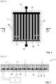
- FIG. 4 shows in front view the bottom plate 3 of a cell 1 comprising a first embodiment of the electrodes 4a and 4b. This figure can be studied alongside the figure 5 which shows the associated cell 1, in section following the plane whose trace AA is represented on the Figure 4 .
- the electrodes 4a and 4b are formed of parallel strips which are arranged alternately.
- the first electrode 4a comprises wide bands Bi and the second electrode 4b comprises narrow bands bi, two consecutive wide bands B1 and B2 being separated from each other by a narrow band b1.
- All the wide bands Bi are electrically connected to each other by a first strip 8a.
- All the narrow strips bi are electrically connected to each other by a second strip 8b.
- the first strip 8a is electrically connected to a first connection track 9a.
- the second strip 8b is electrically connected to a second connection track 9b.
- widths of the wide strips and narrow strips as well as the width of the spaces which separate them can be modified.
- the important thing is to always have at the cell level a significant surface gap between the wide strips and narrow strips while covering a maximum of the surface of the bottom plate 3.
- the space between the wide and narrow bands could be varied between 110 micrometers and 20 micrometers.
- first electrode 4a and the second electrode 4b are possible.
- each tongue Li of a narrow strip Bi is housed in a slot Ci of a wide strip Bi.
- each tongue Li of a wide band Bi is housed in a slot ci of a narrow band bi.
- the slots and tongues are also rectangular in shape.
- This embodiment results in greater coverage of the surface of the bottom plate. This variant also helps reduce particle accumulation.
- FIG. 6b shows another embodiment which is similar to that of the figure 6a but for which the slots Ci/ci and tongues Li/li are triangular in shape.
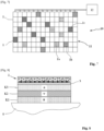
- FIG 7 shows a device 10 for controlling infrared reflectivity which uses several cells 1 assembled on a common support 11, for example a canvas or a rigid plate carried by a structure.
- All cells 1 have a structure of the type described previously. But each cell 1 can be controlled individually by a control means 12 equipped with means allowing it, by addressing, to apply a particular voltage to each cell 1 to give it a particular emissive or reflective state.
- This state will be defined by calculation means incorporated in the control means 12 and which will be associated for example with camera means allowing it to determine the infrared emission or absorption characteristics of the medium surrounding the structure carrying the device. For example, we can consult the patent EP2992292 which describes such a device.
- the device 10 a particular infrared signature that varies from cell to cell.
- figure 7 cells 1a, 1b, 1c having different emissive or reflective states.
- FIG 8 shows a cell 1 whose bottom plate 3 is transparent in the visible range. It is positioned on three cells K1, K2 and K3 containing cholesteric liquid crystals making it possible to obtain a coloring which is respectively: blue for K1, green for K2 and red for K3. Each cell K1, K2 and K3 can be controlled individually by a control means with a more or less intense dosage of each color.
- the stack of cells 1, K1, K2 and K3 is fixed on a structure S to be camouflaged.
Landscapes
- Physics & Mathematics (AREA)
- Nonlinear Science (AREA)
- Optics & Photonics (AREA)
- General Physics & Mathematics (AREA)
- Chemical & Material Sciences (AREA)
- Electrochemistry (AREA)
- Molecular Biology (AREA)
- Health & Medical Sciences (AREA)
- Chemical Kinetics & Catalysis (AREA)
- Life Sciences & Earth Sciences (AREA)
- Geometry (AREA)
- Mathematical Physics (AREA)
- Crystallography & Structural Chemistry (AREA)
- Electrochromic Elements, Electrophoresis, Or Variable Reflection Or Absorption Elements (AREA)
- Special Wing (AREA)
- Glass Compositions (AREA)
- Laser Beam Printer (AREA)
- Threshing Machine Elements (AREA)
Applications Claiming Priority (2)
| Application Number | Priority Date | Filing Date | Title |
|---|---|---|---|
| FR2003338A FR3109219B1 (fr) | 2020-04-08 | 2020-04-08 | Dispositif de contrôle de la réflectivité infrarouge |
| PCT/IB2021/052578 WO2021205280A1 (fr) | 2020-04-08 | 2021-03-29 | Dispositif de contrôle de la réflectivité infrarouge |
Publications (2)
| Publication Number | Publication Date |
|---|---|
| EP4133330A1 EP4133330A1 (fr) | 2023-02-15 |
| EP4133330B1 true EP4133330B1 (fr) | 2024-08-07 |
Family
ID=72178645
Family Applications (1)
| Application Number | Title | Priority Date | Filing Date |
|---|---|---|---|
| EP21718966.1A Active EP4133330B1 (fr) | 2020-04-08 | 2021-03-29 | Dispositif de contrôle de la réflectivité infrarouge |
Country Status (11)
| Country | Link |
|---|---|
| EP (1) | EP4133330B1 (da) |
| AU (1) | AU2021252630B2 (da) |
| DK (1) | DK4133330T3 (da) |
| ES (1) | ES2993321T3 (da) |
| FI (1) | FI4133330T3 (da) |
| FR (1) | FR3109219B1 (da) |
| HU (1) | HUE068991T2 (da) |
| IL (1) | IL297140B1 (da) |
| LT (1) | LT4133330T (da) |
| PL (1) | PL4133330T3 (da) |
| WO (1) | WO2021205280A1 (da) |
Families Citing this family (1)
| Publication number | Priority date | Publication date | Assignee | Title |
|---|---|---|---|---|
| WO2025043712A1 (zh) * | 2023-09-01 | 2025-03-06 | 京东方科技集团股份有限公司 | 调光面板及其控制方法、调光结构以及调光装置 |
Citations (1)
| Publication number | Priority date | Publication date | Assignee | Title |
|---|---|---|---|---|
| JPS604828A (ja) * | 1983-06-23 | 1985-01-11 | Matsushita Electric Ind Co Ltd | 赤外線変調器 |
Family Cites Families (7)
| Publication number | Priority date | Publication date | Assignee | Title |
|---|---|---|---|---|
| US7956841B2 (en) * | 1995-07-20 | 2011-06-07 | E Ink Corporation | Stylus-based addressing structures for displays |
| ATE402428T1 (de) * | 2002-02-19 | 2008-08-15 | Koninkl Philips Electronics Nv | Elektrophoretische anzeigevorrichtung |
| CN103926778A (zh) * | 2006-07-11 | 2014-07-16 | 皇家飞利浦电子股份有限公司 | 电泳设备及其控制方法 |
| FR3005350B1 (fr) | 2013-05-03 | 2015-04-17 | Nexter Systems | Procede et dispositif de masquage adaptatif. |
| FR3028052B1 (fr) | 2014-10-31 | 2017-12-08 | Nexter Systems | Cellule reflechissante a reflectivite modulable |
| US10852615B2 (en) * | 2014-12-02 | 2020-12-01 | University Of Cincinnati | Two particle electrophoretic laminate for use with smart windows with reduced diffraction |
| US10642121B2 (en) | 2017-03-02 | 2020-05-05 | Korea Electronics Technology Institute | Reflective display device for visible light and infrared camouflage and active camouflage device using the same |
-
2020
- 2020-04-08 FR FR2003338A patent/FR3109219B1/fr active Active
-
2021
- 2021-03-29 EP EP21718966.1A patent/EP4133330B1/fr active Active
- 2021-03-29 AU AU2021252630A patent/AU2021252630B2/en active Active
- 2021-03-29 HU HUE21718966A patent/HUE068991T2/hu unknown
- 2021-03-29 DK DK21718966.1T patent/DK4133330T3/da active
- 2021-03-29 WO PCT/IB2021/052578 patent/WO2021205280A1/fr not_active Ceased
- 2021-03-29 ES ES21718966T patent/ES2993321T3/es active Active
- 2021-03-29 PL PL21718966.1T patent/PL4133330T3/pl unknown
- 2021-03-29 LT LTEPPCT/IB2021/052578T patent/LT4133330T/lt unknown
- 2021-03-29 FI FIEP21718966.1T patent/FI4133330T3/fi active
- 2021-03-30 IL IL297140A patent/IL297140B1/en unknown
Patent Citations (1)
| Publication number | Priority date | Publication date | Assignee | Title |
|---|---|---|---|---|
| JPS604828A (ja) * | 1983-06-23 | 1985-01-11 | Matsushita Electric Ind Co Ltd | 赤外線変調器 |
Also Published As
| Publication number | Publication date |
|---|---|
| LT4133330T (lt) | 2025-01-10 |
| EP4133330A1 (fr) | 2023-02-15 |
| FR3109219B1 (fr) | 2024-03-29 |
| IL297140B1 (en) | 2026-04-01 |
| AU2021252630A1 (en) | 2022-11-03 |
| AU2021252630B2 (en) | 2025-04-17 |
| PL4133330T3 (pl) | 2024-12-02 |
| DK4133330T3 (da) | 2024-09-09 |
| FI4133330T3 (fi) | 2024-09-26 |
| FR3109219A1 (fr) | 2021-10-15 |
| HUE068991T2 (hu) | 2025-02-28 |
| ES2993321T3 (en) | 2024-12-27 |
| WO2021205280A1 (fr) | 2021-10-14 |
| IL297140A (en) | 2022-12-01 |
Similar Documents
| Publication | Publication Date | Title |
|---|---|---|
| EP0872759B1 (fr) | Dispositif d'affichage à cristaux liquides destiné notamment à former un écran d'affichage d'images en couleur | |
| CA2769194C (fr) | Systeme electrochrome transparent | |
| CH616243A5 (da) | ||
| TW202328789A (zh) | 在開啟狀態下具有降低的繞射的電泳粒子膜 | |
| EP0202974A1 (fr) | Ecran matriciel à couleurs, sa fabrication et dispositif comprenant un tel écran | |
| US11506917B2 (en) | Optical device for forming a distribution of a three-dimensional light field | |
| WO2010076471A1 (fr) | Element optique a puissance variable | |
| EP4133330B1 (fr) | Dispositif de contrôle de la réflectivité infrarouge | |
| FR2526177A1 (fr) | Perfectionnements aux cellules optiques utilisant des cristaux liquides | |
| CA1314615C (fr) | Modulateur d'onde electromagnetique a puits quantiques couples, et application a un detecteur d'onde electromagnetique | |
| EP3265541A1 (fr) | Matériau destiné à la réalisation d'un dispositif d'obturation électro-optique à trois états de transmission, dispositif et utilisations correspondants | |
| EP3213146B1 (fr) | Cellule reflechissante a reflectivite modulable | |
| EP1627421A2 (fr) | Structure amorphe de couplage optique pour detecteur d ondes electromagnetiques et detecteur associe | |
| EP0063077A1 (fr) | Procédé de commande d'un dispositif de visualisation | |
| EP0731374A1 (fr) | Ecran à cristaux liquides à angle de vue amélioré | |
| FR3143716A1 (fr) | Dispositif lumineux de véhicule comportant un guide de lumière muni d’une structure multicouche | |
| FR2772149A1 (fr) | Cellule de pockels et interrupteur optique a cellule de pockels | |
| WO2008125489A1 (fr) | Procede de fabrication d'une cellule electro-optique a base de psflc et/ou psaflc, cellule electro-optique, dispositif et casque correspondants | |
| EP4198623B1 (fr) | Dispositif de modulation de phase à cristal liquide | |
| EP3218447A1 (fr) | Cellule a cristal liquide cholesterique a reflectivite augmentee | |
| EP4038447B1 (fr) | Modulateur spatial de lumiere adresse thermo-optiquement | |
| CH625630A5 (da) | ||
| EP3798696A1 (fr) | Structure diffusive pour source de lumière | |
| FR3021800A1 (fr) | Dispositif d'affichage reflectif a tres haute luminosite et a surface photovoltaique integree | |
| WO2017167922A1 (fr) | Dispositif d'obturation électro-optique à double état de transmission optimisé sur l'ensemble de la bande spectrale du visible |
Legal Events
| Date | Code | Title | Description |
|---|---|---|---|
| STAA | Information on the status of an ep patent application or granted ep patent |
Free format text: STATUS: UNKNOWN |
|
| STAA | Information on the status of an ep patent application or granted ep patent |
Free format text: STATUS: THE INTERNATIONAL PUBLICATION HAS BEEN MADE |
|
| PUAI | Public reference made under article 153(3) epc to a published international application that has entered the european phase |
Free format text: ORIGINAL CODE: 0009012 |
|
| STAA | Information on the status of an ep patent application or granted ep patent |
Free format text: STATUS: REQUEST FOR EXAMINATION WAS MADE |
|
| 17P | Request for examination filed |
Effective date: 20221104 |
|
| AK | Designated contracting states |
Kind code of ref document: A1 Designated state(s): AL AT BE BG CH CY CZ DE DK EE ES FI FR GB GR HR HU IE IS IT LI LT LU LV MC MK MT NL NO PL PT RO RS SE SI SK SM TR |
|
| DAV | Request for validation of the european patent (deleted) | ||
| DAX | Request for extension of the european patent (deleted) | ||
| GRAP | Despatch of communication of intention to grant a patent |
Free format text: ORIGINAL CODE: EPIDOSNIGR1 |
|
| STAA | Information on the status of an ep patent application or granted ep patent |
Free format text: STATUS: GRANT OF PATENT IS INTENDED |
|
| RIC1 | Information provided on ipc code assigned before grant |
Ipc: G02F 1/1343 20060101ALI20240221BHEP Ipc: G02F 1/16761 20190101ALI20240221BHEP Ipc: G02F 1/16762 20190101ALI20240221BHEP Ipc: G02F 1/1677 20190101ALI20240221BHEP Ipc: G02F 1/1676 20190101ALI20240221BHEP Ipc: G02F 1/1675 20190101ALI20240221BHEP Ipc: G02F 1/167 20190101AFI20240221BHEP |
|
| INTG | Intention to grant announced |
Effective date: 20240311 |
|
| RAP3 | Party data changed (applicant data changed or rights of an application transferred) |
Owner name: CY CERGY PARIS UNIVERSITE Owner name: INSTITUT MINES TELECOM Owner name: KNDS FRANCE |
|
| GRAS | Grant fee paid |
Free format text: ORIGINAL CODE: EPIDOSNIGR3 |
|
| GRAA | (expected) grant |
Free format text: ORIGINAL CODE: 0009210 |
|
| STAA | Information on the status of an ep patent application or granted ep patent |
Free format text: STATUS: THE PATENT HAS BEEN GRANTED |
|
| AK | Designated contracting states |
Kind code of ref document: B1 Designated state(s): AL AT BE BG CH CY CZ DE DK EE ES FI FR GB GR HR HU IE IS IT LI LT LU LV MC MK MT NL NO PL PT RO RS SE SI SK SM TR |
|
| REG | Reference to a national code |
Ref country code: GB Ref legal event code: FG4D Free format text: NOT ENGLISH |
|
| REG | Reference to a national code |
Ref country code: CH Ref legal event code: EP |
|
| REG | Reference to a national code |
Ref country code: IE Ref legal event code: FG4D Free format text: LANGUAGE OF EP DOCUMENT: FRENCH |
|
| REG | Reference to a national code |
Ref country code: DE Ref legal event code: R096 Ref document number: 602021016828 Country of ref document: DE |
|
| REG | Reference to a national code |
Ref country code: DK Ref legal event code: T3 Effective date: 20240906 |
|
| REG | Reference to a national code |
Ref country code: FI Ref legal event code: FGE |
|
| REG | Reference to a national code |
Ref country code: SE Ref legal event code: TRGR |
|
| REG | Reference to a national code |
Ref country code: NL Ref legal event code: FP |
|
| REG | Reference to a national code |
Ref country code: EE Ref legal event code: FG4A Ref document number: E024716 Country of ref document: EE Effective date: 20241017 |
|
| REG | Reference to a national code |
Ref country code: ES Ref legal event code: FG2A Ref document number: 2993321 Country of ref document: ES Kind code of ref document: T3 Effective date: 20241227 |
|
| REG | Reference to a national code |
Ref country code: AT Ref legal event code: MK05 Ref document number: 1711603 Country of ref document: AT Kind code of ref document: T Effective date: 20240807 |
|
| PG25 | Lapsed in a contracting state [announced via postgrant information from national office to epo] |
Ref country code: GR Free format text: LAPSE BECAUSE OF FAILURE TO SUBMIT A TRANSLATION OF THE DESCRIPTION OR TO PAY THE FEE WITHIN THE PRESCRIBED TIME-LIMIT Effective date: 20241108 Ref country code: PT Free format text: LAPSE BECAUSE OF FAILURE TO SUBMIT A TRANSLATION OF THE DESCRIPTION OR TO PAY THE FEE WITHIN THE PRESCRIBED TIME-LIMIT Effective date: 20241209 |
|
| PG25 | Lapsed in a contracting state [announced via postgrant information from national office to epo] |
Ref country code: BG Free format text: LAPSE BECAUSE OF FAILURE TO SUBMIT A TRANSLATION OF THE DESCRIPTION OR TO PAY THE FEE WITHIN THE PRESCRIBED TIME-LIMIT Effective date: 20240807 |
|
| PG25 | Lapsed in a contracting state [announced via postgrant information from national office to epo] |
Ref country code: LV Free format text: LAPSE BECAUSE OF FAILURE TO SUBMIT A TRANSLATION OF THE DESCRIPTION OR TO PAY THE FEE WITHIN THE PRESCRIBED TIME-LIMIT Effective date: 20240807 |
|
| PG25 | Lapsed in a contracting state [announced via postgrant information from national office to epo] |
Ref country code: AT Free format text: LAPSE BECAUSE OF FAILURE TO SUBMIT A TRANSLATION OF THE DESCRIPTION OR TO PAY THE FEE WITHIN THE PRESCRIBED TIME-LIMIT Effective date: 20240807 Ref country code: IS Free format text: LAPSE BECAUSE OF FAILURE TO SUBMIT A TRANSLATION OF THE DESCRIPTION OR TO PAY THE FEE WITHIN THE PRESCRIBED TIME-LIMIT Effective date: 20241207 |
|
| PG25 | Lapsed in a contracting state [announced via postgrant information from national office to epo] |
Ref country code: HR Free format text: LAPSE BECAUSE OF FAILURE TO SUBMIT A TRANSLATION OF THE DESCRIPTION OR TO PAY THE FEE WITHIN THE PRESCRIBED TIME-LIMIT Effective date: 20240807 |
|
| PG25 | Lapsed in a contracting state [announced via postgrant information from national office to epo] |
Ref country code: RS Free format text: LAPSE BECAUSE OF FAILURE TO SUBMIT A TRANSLATION OF THE DESCRIPTION OR TO PAY THE FEE WITHIN THE PRESCRIBED TIME-LIMIT Effective date: 20241107 |
|
| PG25 | Lapsed in a contracting state [announced via postgrant information from national office to epo] |
Ref country code: RS Free format text: LAPSE BECAUSE OF FAILURE TO SUBMIT A TRANSLATION OF THE DESCRIPTION OR TO PAY THE FEE WITHIN THE PRESCRIBED TIME-LIMIT Effective date: 20241107 Ref country code: PT Free format text: LAPSE BECAUSE OF FAILURE TO SUBMIT A TRANSLATION OF THE DESCRIPTION OR TO PAY THE FEE WITHIN THE PRESCRIBED TIME-LIMIT Effective date: 20241209 Ref country code: LV Free format text: LAPSE BECAUSE OF FAILURE TO SUBMIT A TRANSLATION OF THE DESCRIPTION OR TO PAY THE FEE WITHIN THE PRESCRIBED TIME-LIMIT Effective date: 20240807 Ref country code: IS Free format text: LAPSE BECAUSE OF FAILURE TO SUBMIT A TRANSLATION OF THE DESCRIPTION OR TO PAY THE FEE WITHIN THE PRESCRIBED TIME-LIMIT Effective date: 20241207 Ref country code: HR Free format text: LAPSE BECAUSE OF FAILURE TO SUBMIT A TRANSLATION OF THE DESCRIPTION OR TO PAY THE FEE WITHIN THE PRESCRIBED TIME-LIMIT Effective date: 20240807 Ref country code: GR Free format text: LAPSE BECAUSE OF FAILURE TO SUBMIT A TRANSLATION OF THE DESCRIPTION OR TO PAY THE FEE WITHIN THE PRESCRIBED TIME-LIMIT Effective date: 20241108 Ref country code: BG Free format text: LAPSE BECAUSE OF FAILURE TO SUBMIT A TRANSLATION OF THE DESCRIPTION OR TO PAY THE FEE WITHIN THE PRESCRIBED TIME-LIMIT Effective date: 20240807 Ref country code: AT Free format text: LAPSE BECAUSE OF FAILURE TO SUBMIT A TRANSLATION OF THE DESCRIPTION OR TO PAY THE FEE WITHIN THE PRESCRIBED TIME-LIMIT Effective date: 20240807 |
|
| REG | Reference to a national code |
Ref country code: HU Ref legal event code: AG4A Ref document number: E068991 Country of ref document: HU |
|
| PG25 | Lapsed in a contracting state [announced via postgrant information from national office to epo] |
Ref country code: SM Free format text: LAPSE BECAUSE OF FAILURE TO SUBMIT A TRANSLATION OF THE DESCRIPTION OR TO PAY THE FEE WITHIN THE PRESCRIBED TIME-LIMIT Effective date: 20240807 |
|
| PG25 | Lapsed in a contracting state [announced via postgrant information from national office to epo] |
Ref country code: SK Free format text: LAPSE BECAUSE OF FAILURE TO SUBMIT A TRANSLATION OF THE DESCRIPTION OR TO PAY THE FEE WITHIN THE PRESCRIBED TIME-LIMIT Effective date: 20240807 |
|
| REG | Reference to a national code |
Ref country code: DE Ref legal event code: R097 Ref document number: 602021016828 Country of ref document: DE |
|
| PLBE | No opposition filed within time limit |
Free format text: ORIGINAL CODE: 0009261 |
|
| STAA | Information on the status of an ep patent application or granted ep patent |
Free format text: STATUS: NO OPPOSITION FILED WITHIN TIME LIMIT |
|
| PGFP | Annual fee paid to national office [announced via postgrant information from national office to epo] |
Ref country code: ES Payment date: 20250401 Year of fee payment: 5 |
|
| 26N | No opposition filed |
Effective date: 20250508 |
|
| PGFP | Annual fee paid to national office [announced via postgrant information from national office to epo] |
Ref country code: CH Payment date: 20250401 Year of fee payment: 5 |
|
| PG25 | Lapsed in a contracting state [announced via postgrant information from national office to epo] |
Ref country code: MC Free format text: LAPSE BECAUSE OF FAILURE TO SUBMIT A TRANSLATION OF THE DESCRIPTION OR TO PAY THE FEE WITHIN THE PRESCRIBED TIME-LIMIT Effective date: 20240807 |
|
| PG25 | Lapsed in a contracting state [announced via postgrant information from national office to epo] |
Ref country code: LU Free format text: LAPSE BECAUSE OF NON-PAYMENT OF DUE FEES Effective date: 20250329 |
|
| PG25 | Lapsed in a contracting state [announced via postgrant information from national office to epo] |
Ref country code: IT Free format text: LAPSE BECAUSE OF NON-PAYMENT OF DUE FEES Effective date: 20250329 |
|
| PG25 | Lapsed in a contracting state [announced via postgrant information from national office to epo] |
Ref country code: IE Free format text: LAPSE BECAUSE OF NON-PAYMENT OF DUE FEES Effective date: 20250329 |
|
| PGFP | Annual fee paid to national office [announced via postgrant information from national office to epo] |
Ref country code: NL Payment date: 20260219 Year of fee payment: 6 |
|
| REG | Reference to a national code |
Ref country code: CH Ref legal event code: U11 Free format text: ST27 STATUS EVENT CODE: U-0-0-U10-U11 (AS PROVIDED BY THE NATIONAL OFFICE) Effective date: 20260401 |
|
| PGFP | Annual fee paid to national office [announced via postgrant information from national office to epo] |
Ref country code: SE Payment date: 20260219 Year of fee payment: 6 |
|
| PGFP | Annual fee paid to national office [announced via postgrant information from national office to epo] |
Ref country code: GB Payment date: 20260219 Year of fee payment: 6 Ref country code: LT Payment date: 20260219 Year of fee payment: 6 |
|
| PGFP | Annual fee paid to national office [announced via postgrant information from national office to epo] |
Ref country code: NO Payment date: 20260223 Year of fee payment: 6 Ref country code: DK Payment date: 20260219 Year of fee payment: 6 Ref country code: DE Payment date: 20260219 Year of fee payment: 6 |
|
| PG25 | Lapsed in a contracting state [announced via postgrant information from national office to epo] |
Ref country code: IT Free format text: LAPSE BECAUSE OF NON-PAYMENT OF DUE FEES Effective date: 20250329 Ref country code: RO Free format text: LAPSE BECAUSE OF FAILURE TO SUBMIT A TRANSLATION OF THE DESCRIPTION OR TO PAY THE FEE WITHIN THE PRESCRIBED TIME-LIMIT Effective date: 20240807 |
|
| PGFP | Annual fee paid to national office [announced via postgrant information from national office to epo] |
Ref country code: FI Payment date: 20260219 Year of fee payment: 6 Ref country code: BE Payment date: 20260219 Year of fee payment: 6 Ref country code: IT Payment date: 20260219 Year of fee payment: 6 |
|
| PGRI | Patent reinstated in contracting state [announced from national office to epo] |
Ref country code: IT Effective date: 20250731 |
|
| PGFP | Annual fee paid to national office [announced via postgrant information from national office to epo] |
Ref country code: HU Payment date: 20260313 Year of fee payment: 6 |
|
| PGFP | Annual fee paid to national office [announced via postgrant information from national office to epo] |
Ref country code: FR Payment date: 20260219 Year of fee payment: 6 |
|
| PGFP | Annual fee paid to national office [announced via postgrant information from national office to epo] |
Ref country code: CZ Payment date: 20260302 Year of fee payment: 6 |
|
| PGFP | Annual fee paid to national office [announced via postgrant information from national office to epo] |
Ref country code: PL Payment date: 20260220 Year of fee payment: 6 |
|
| PGFP | Annual fee paid to national office [announced via postgrant information from national office to epo] |
Ref country code: EE Payment date: 20260227 Year of fee payment: 6 |