EP4131640A1 - Vorrichtung zur reflexion elektromagnetischer wellen, reflexionszaun für elektromagnetische wellen und verfahren zur montage der vorrichtung zur reflexion elektromagnetischer wellen - Google Patents
Vorrichtung zur reflexion elektromagnetischer wellen, reflexionszaun für elektromagnetische wellen und verfahren zur montage der vorrichtung zur reflexion elektromagnetischer wellen Download PDFInfo
- Publication number
- EP4131640A1 EP4131640A1 EP20928670.7A EP20928670A EP4131640A1 EP 4131640 A1 EP4131640 A1 EP 4131640A1 EP 20928670 A EP20928670 A EP 20928670A EP 4131640 A1 EP4131640 A1 EP 4131640A1
- Authority
- EP
- European Patent Office
- Prior art keywords
- electromagnetic wave
- panel
- reflector
- reflection
- angle
- Prior art date
- Legal status (The legal status is an assumption and is not a legal conclusion. Google has not performed a legal analysis and makes no representation as to the accuracy of the status listed.)
- Pending
Links
Images


Classifications
-
- H—ELECTRICITY
- H01—ELECTRIC ELEMENTS
- H01Q—ANTENNAS, i.e. RADIO AERIALS
- H01Q1/00—Details of, or arrangements associated with, antennas
- H01Q1/12—Supports; Mounting means
-
- H—ELECTRICITY
- H01—ELECTRIC ELEMENTS
- H01Q—ANTENNAS, i.e. RADIO AERIALS
- H01Q15/00—Devices for reflection, refraction, diffraction or polarisation of waves radiated from an antenna, e.g. quasi-optical devices
- H01Q15/0006—Devices acting selectively as reflecting surface, as diffracting or as refracting device, e.g. frequency filtering or angular spatial filtering devices
- H01Q15/0086—Devices acting selectively as reflecting surface, as diffracting or as refracting device, e.g. frequency filtering or angular spatial filtering devices said selective devices having materials with a synthesized negative refractive index, e.g. metamaterials or left-handed materials
-
- H—ELECTRICITY
- H01—ELECTRIC ELEMENTS
- H01Q—ANTENNAS, i.e. RADIO AERIALS
- H01Q1/00—Details of, or arrangements associated with, antennas
- H01Q1/12—Supports; Mounting means
- H01Q1/1207—Supports; Mounting means for fastening a rigid aerial element
-
- H—ELECTRICITY
- H01—ELECTRIC ELEMENTS
- H01Q—ANTENNAS, i.e. RADIO AERIALS
- H01Q1/00—Details of, or arrangements associated with, antennas
- H01Q1/12—Supports; Mounting means
- H01Q1/1242—Rigid masts specially adapted for supporting an aerial
-
- H—ELECTRICITY
- H01—ELECTRIC ELEMENTS
- H01Q—ANTENNAS, i.e. RADIO AERIALS
- H01Q1/00—Details of, or arrangements associated with, antennas
- H01Q1/12—Supports; Mounting means
- H01Q1/125—Means for positioning
-
- H—ELECTRICITY
- H01—ELECTRIC ELEMENTS
- H01Q—ANTENNAS, i.e. RADIO AERIALS
- H01Q15/00—Devices for reflection, refraction, diffraction or polarisation of waves radiated from an antenna, e.g. quasi-optical devices
- H01Q15/14—Reflecting surfaces; Equivalent structures
-
- H—ELECTRICITY
- H01—ELECTRIC ELEMENTS
- H01Q—ANTENNAS, i.e. RADIO AERIALS
- H01Q15/00—Devices for reflection, refraction, diffraction or polarisation of waves radiated from an antenna, e.g. quasi-optical devices
- H01Q15/14—Reflecting surfaces; Equivalent structures
- H01Q15/141—Apparatus or processes specially adapted for manufacturing reflecting surfaces
- H01Q15/142—Apparatus or processes specially adapted for manufacturing reflecting surfaces using insulating material for supporting the reflecting surface
-
- H—ELECTRICITY
- H01—ELECTRIC ELEMENTS
- H01Q—ANTENNAS, i.e. RADIO AERIALS
- H01Q19/00—Combinations of primary active antenna elements and units with secondary devices, e.g. with quasi-optical devices, for giving the antenna a desired directional characteristic
- H01Q19/10—Combinations of primary active antenna elements and units with secondary devices, e.g. with quasi-optical devices, for giving the antenna a desired directional characteristic using reflecting surfaces
- H01Q19/104—Combinations of primary active antenna elements and units with secondary devices, e.g. with quasi-optical devices, for giving the antenna a desired directional characteristic using reflecting surfaces using a substantially flat reflector for deflecting the radiated beam, e.g. periscopic antennas
-
- H—ELECTRICITY
- H01—ELECTRIC ELEMENTS
- H01Q—ANTENNAS, i.e. RADIO AERIALS
- H01Q3/00—Arrangements for changing or varying the orientation or the shape of the directional pattern of the waves radiated from an antenna or antenna system
- H01Q3/12—Arrangements for changing or varying the orientation or the shape of the directional pattern of the waves radiated from an antenna or antenna system using mechanical relative movement between primary active elements and secondary devices of antennas or antenna systems
- H01Q3/16—Arrangements for changing or varying the orientation or the shape of the directional pattern of the waves radiated from an antenna or antenna system using mechanical relative movement between primary active elements and secondary devices of antennas or antenna systems for varying relative position of primary active element and a reflecting device
- H01Q3/20—Arrangements for changing or varying the orientation or the shape of the directional pattern of the waves radiated from an antenna or antenna system using mechanical relative movement between primary active elements and secondary devices of antennas or antenna systems for varying relative position of primary active element and a reflecting device wherein the primary active element is fixed and the reflecting device is movable
-
- H—ELECTRICITY
- H05—ELECTRIC TECHNIQUES NOT OTHERWISE PROVIDED FOR
- H05K—PRINTED CIRCUITS; CASINGS OR CONSTRUCTIONAL DETAILS OF ELECTRIC APPARATUS; MANUFACTURE OF ASSEMBLAGES OF ELECTRICAL COMPONENTS
- H05K9/00—Screening of apparatus or components against electric or magnetic fields
-
- H—ELECTRICITY
- H05—ELECTRIC TECHNIQUES NOT OTHERWISE PROVIDED FOR
- H05K—PRINTED CIRCUITS; CASINGS OR CONSTRUCTIONAL DETAILS OF ELECTRIC APPARATUS; MANUFACTURE OF ASSEMBLAGES OF ELECTRICAL COMPONENTS
- H05K9/00—Screening of apparatus or components against electric or magnetic fields
- H05K9/0001—Rooms or chambers
Definitions
- the base stations BS1 and BS2 may cooperate with each other to improve the coverage and the quality of radio communication. The details of the positional relationship of the base stations BS with respect to the production line will be described later.
- the wireless communication quality could be maintained by providing a large number of base stations along the longitudinal axis of the production line 3; however, efficient use of the work space is disturbed and installation cost will increase.
- the wireless transmission system 1 solves these problems by providing an electromagnetic wave reflector 10 along the longitudinal axis of the production line 3, and by providing a base station BS at an end of the production line 3 in the longitudinal direction. Owing to the electromagnetic wave reflector 10, the number of base stations installed in the production facility can be reduced, and the wireless communication environment between the base station BS and equipment and devices in the production line 3 can be improved.
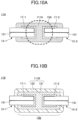
- FIG. 5B shows an electromagnetic wave reflector 10B, in which a brace 19 is provided on the back surface of the panel 13, opposite to the reflective surface 105, to reinforce or increase the rigidity of the panel 13 of the electromagnetic wave reflector 10B.
- the brace 19 may be bridged between the support bodies 11 holding opposite edges of the panel 13.
- FIG. 5A to FIG. 5D can be combined with each other.
- the meta-reflector 102 may be held in a movable manner on the reflective surface 105, while the brace 19 of FIG. 5B may be provided on the back surface opposite to the reflective surface 105.
- the reflective surface 105 By designing the reflective surface 105 to reflect radio waves of a desired frequency band from 1 GHz to 170 GHz, a wide range of communication bands can be covered, including 1.5 GHz band and 2.5 GHz band currently used in Japan as the main frequency bands of mobile communications, and 4.5 GHz band and 28 GHz band scheduled for the next-generation 5G mobile communications network. In foreign countries, 2.5 GHz band, 3.5 GHz band, 4.5 GHz band, 24 to 28 GHz band, and 39 GHz band are planned for the 5G frequency band.
- the electromagnetic wave reflector of the embodiment is capable of dealing with these frequency bands, as well as 52.6 GHz band which is the upper limit of the 5G standardized millimeter wave band.
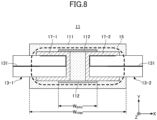
- the electrical connector part 15 includes conductive edge jackets 17-1 and 17-2 (which may be collectively referred to as "edge jackets 17") that receive the edges of the panels 13, and bridge electrodes 112 electrically connecting the edge jackets 17 to the adjacent panels.
- the bridge electrode 112 is an example of a conductive bridge that bridges the potential surfaces of the panels 13-1 and 13-2.
- the edge jacket 17-1 gripping the edge of the panel 13-1 and the edge jacket 17-1 gripping the edge of the panel 13-2 are electrically connected to each other by the bridge electrodes 112.
- the bridge electrodes 112 are in surface contact with the edge jackets 17-1 and 17-2 to ensure the electrical connection.
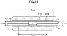
- the width W BRG of the bridge electrode 112 which serves as a conductive bridge, is preferably 100 mm or less, more preferably from 10 mm to 50 mm, from the viewpoint of sharing the potential surface of reflection between the panels 13 with the smallest possible size.
- the thickness of the bridge electrode 112 is preferably 20 mm or less, more preferably 10 mm or less, and even more preferably from 1 mm to 5 mm. The grounds for the preferable range of the widths and thicknesses of the frame 111 and the bridge electrode 112 will be described later with reference to FIG. 14 and the subsequent figures.
- the CFRP holding the edge jackets 17-1 and 17-2 serves by itself as the electrical connector part 15A. Electrical connection can be established between the edge jackets 17-1 and 17-2 without using a bridge electrode 112.
- the carbon fiber content ratio of CFRP is 50% or more, 60% or more, 70% or more, 80% or more, or even 90% or more.
- the resin content ratio of CFRP is preferably 50% or less, 40% or less, 30% or less, 20% or less, or even 10% or less.
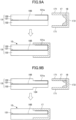
- FIG. 10D shows a configuration of an electrical connector part 15D of a support body 11D.
- the electrical connector part 15D has a bridge electrode 114 that electrically connects the edge jackets 17-1 and 17-2.
- the bridge electrode 114 connects the bottom surfaces 172 of the edge jackets 17-1 and 17-2.
- the configuration of FIG. 10D is advantageous in that the high frequency current can flow in the shortest path from the conductor 131-1 along the shortest path through the edge jacket 17-1, the bridge electrode 114, the edge jacket 17-2, and the conductor 131-2.
- FIG. 10F shows a configuration using a frame 111F of a composite type of metal and resin.
- the frame 111F has a metal connector 141 and a resin reinforcement 142 that covers the metal connector 141.
- the metal connector 141 can be easily manufactured by extrusion molding or the like, and the connector itself has a certain degree of strength while ensuring electrical connection.
- the resin reinforcement 142 may be formed of an adhesive such as an acrylic adhesive or an epoxy adhesive, thereby reducing the thickness of the metal connector 141 and suppressing residual inductance caused by current detours.
- the corners may be rounded to prevent diffraction at the corners.
- FIG. 10H shows a structure using a commercially available frame 1100 formed by extrusion molding of aluminum as a reference example.
- the frame 1100 having a complicated cross-sectional shape, currents flow in various directions, and residual inductance and stray capacitance are generated due to the complicated current detour paths.
- the response varies in a complicated manner, depending on the incident electromagnetic waves, and the sharing or propagation of the reference potential of reflection is adversely affected. For these reasons, it is preferable to adopt the configurations of the electrical connector part 15 shown in FIG. 8 and FIG. 10A to FIG. 10G for the frame body 11.
- the frame 111 is configured to be adaptable to the guide beam 118 attached to another electromagnetic wave reflector 10, while the guide beam 118 is configured to be able to receive the frame 111 attached to another electromagnetic wave reflector 10.
- the guide beam 118 of the electromagnetic wave reflector 10-1 receives the frame 111 of the electromagnetic wave reflector 10-2.
- the guide beam 118 of the electromagnetic wave reflector 10-2 receives the frame 111 of the electromagnetic wave reflector 10-3.
- FIG. 11C shows the state of the electromagnetic wave reflectors 10 after connection.
- the frame 111 together with the guide beams 118, form the support body 11.
- a plurality of electromagnetic wave reflectors 10-1, 10-2, and 10-3 can be connected by the support body 11 to form an electromagnetic wave reflective fence 100.
- the electrical connector part 15 of the frame 111 can suppress discontinuity of the reflected current waves at the boundary between the panels 13.
- the performance to reflect the incident electromagnetic waves is evaluated by a radar reflection cross section (RCS), that is, a scattering cross section.
- the unit of RCS is square meters (sm).
- the frame thickness T FRM is fixed to 1 mm, and the peak intensity ratio of the scattering cross section is calculated, while changing the frame width W FRM from 0 mm to 150 mm.
- the frame width W FRM is fixed to 50 mm, and the peak intensity ratio of the scattering cross section (hereinafter referred to simply as "peak ratio") is calculated, while changing the frame thickness T FRM from 0 mm to 15 mm.
- the peak ratio of 1.0 represents the reflection characteristic of a single panel without the electrical connector part 15.
- the dashed line indicates the peak ratio of an aluminum frame with a thickness of 10 mm and a width of 50 mm for reference.
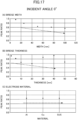
- FIG. 17 shows the relationships between the width and the reflection characteristic, between the thickness and the reflection characteristic, and between material of the bridge electrode and the reflection characteristic when the incident angle is 0°.
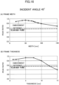
- FIG. 18 shows the relationships between the width and the reflection characteristic, between the thickness and the reflection characteristic, and between material of the bridge electrode and the reflection characteristic when the incident angle is 45°.
- the peak ratio of the scattering cross section is calculated while changing the width W BRG of the bridge electrode in the range from 10 mm to 100 mm.
- FIG. 17 (B) the peak ratio of the scattering cross section is calculated while changing the thickness T BRG of the bridge electrode in the range from 1 mm to 50 mm.
- FIG. 20A and FIG. 20B show analytic space of reflection characteristics of Examples 1 to 8 and Referenced Configurations 1 to 4 described below.
- the thickness direction of the panel is the x direction
- the width direction is the y direction
- the height direction is the z direction.
- the dimensions of the analytic space are represented as (x-direction dimension) ⁇ (y-direction dimension) ⁇ (z-direction dimension).
- the dimensions of the analytic space are 150 mm ⁇ 500 mm ⁇ 500 mm.
- the dimensions of the analytic space are 100 mm ⁇ 200 mm ⁇ 200 mm.
- the analytic space is narrowed at a higher frequency because the wavelength decreases.
- the boundary conditions are designed so as to have a radio wave absorber around the analytic space.
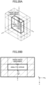
- FIG. 21 shows a simulation model used in Examples and Referenced Configurations.
- a conductor 131 is provided and bonded between two dielectrics 132 and 133.
- the dielectrics 132 and 133 are made of glass or polycarbonate with a thickness of 2 mm.
- the conductor 131 is made of SUS with a thickness of 1 mm.
- the total thickness of the panel 13 is 5 mm.
- a 10 mm gap is provided between the two panels 13. This configuration of the panel 13 is in common throughout Examples 1-8 and Referenced Configurations 1-4.
- an aluminum plate having a thickness of 1 mm and a width of 50 mm is used as the bridge electrode (referred to as "BRG" in the figure) of the electrical connector part 15.
- An FRP frame (referred to as "FRM” in the figure) with a thickness of 5 mm and a width of 50 mm is provided onto the outer surface of the aluminum plate.
- the radius of curvature R at the corners of the frame is 2 mm.
- the frequency of the incident electromagnetic wave is 3.8 GHz.
- the analytic space is set to 150 mm ⁇ 500 mm ⁇ 500 mm.
- the angle of incidence is changed from 0° to 60° with a step size of 10°, and the intensity ratio of the main peak of the scattering cross section is calculated. The calculation results are shown in Table 1.
- each of the meta-reflectors 102 is preferable for each of the meta-reflectors 102 to cover at least the first Fresnel zone.
- the base stations BS are positioned closer to the production line 3 than to the Line L horizontally extending from the reflective surface 105 of the electromagnetic wave reflector 10, but are positioned closer to the center, rather than the ends, of the production line 3 in the longitudinal direction. Pattern 2 is more sensitive to variations in the oblique incidence angle, as will be explained below.
- the anomalous angle ⁇ abn is changed to 7 different angles, namely 20°, 25°, 30°, 35°, 40°, 45°, and 50°, to estimate the fluctuation in the reflection angle with respect to the change in the incident angle.
- the fluctuation in the reflection angle is almost the same at the seven different anomalous angles ⁇ abn, and accordingly, the plotted lines overlap each other, which appear as one thick line in the figure.
- the fluctuation of the reflection angle with respect to the change of the incident angle of 1 degree is as small as less than 1 degree, and is almost constant regardless of the incident angle.
- the reflection controllability in the asymmetric reflection is high. It is easily inferred that the tendency of FIG. 31A exhibiting little fluctuation in the reflection angle can be maintained even at an incident angle exceeding 75° and approaching 90°.
- f x arg Z S x ⁇ ⁇ Z S x + ⁇ , where arg() is a function representing an argument of a complex number.
Landscapes
- Engineering & Computer Science (AREA)
- Physics & Mathematics (AREA)
- Electromagnetism (AREA)
- Microelectronics & Electronic Packaging (AREA)
- Manufacturing & Machinery (AREA)
- Aerials With Secondary Devices (AREA)
- Shielding Devices Or Components To Electric Or Magnetic Fields (AREA)
- Support Of Aerials (AREA)
Applications Claiming Priority (3)
| Application Number | Priority Date | Filing Date | Title |
|---|---|---|---|
| JP2020064577 | 2020-03-31 | ||
| JP2020173308 | 2020-10-14 | ||
| PCT/JP2020/045591 WO2021199503A1 (ja) | 2020-03-31 | 2020-12-08 | 電磁波反射装置、電磁波反射フェンス、及び電磁波反射装置の組み立て方法 |
Publications (2)
| Publication Number | Publication Date |
|---|---|
| EP4131640A1 true EP4131640A1 (de) | 2023-02-08 |
| EP4131640A4 EP4131640A4 (de) | 2024-04-03 |
Family
ID=77928379
Family Applications (1)
| Application Number | Title | Priority Date | Filing Date |
|---|---|---|---|
| EP20928670.7A Pending EP4131640A4 (de) | 2020-03-31 | 2020-12-08 | Vorrichtung zur reflexion elektromagnetischer wellen, reflexionszaun für elektromagnetische wellen und verfahren zur montage der vorrichtung zur reflexion elektromagnetischer wellen |
Country Status (6)
| Country | Link |
|---|---|
| US (2) | US12355154B2 (de) |
| EP (1) | EP4131640A4 (de) |
| JP (2) | JP7517408B2 (de) |
| KR (1) | KR20220161288A (de) |
| CN (2) | CN121507367A (de) |
| WO (1) | WO2021199503A1 (de) |
Families Citing this family (7)
| Publication number | Priority date | Publication date | Assignee | Title |
|---|---|---|---|---|
| EP4131655B1 (de) * | 2020-03-31 | 2025-11-19 | Agc Inc. | Drahtloses übertragungssystem |
| CN116941135A (zh) * | 2021-03-16 | 2023-10-24 | Agc株式会社 | 电磁波反射装置、电磁波反射围栏以及电磁波反射装置的组装方法 |
| EP4525211A1 (de) * | 2022-05-09 | 2025-03-19 | Agc Inc. | Vorrichtung zur reflexion elektromagnetischer wellen und reflexionszaun für elektromagnetische wellen |
| US20250357675A1 (en) * | 2022-05-31 | 2025-11-20 | Kyocera Corporation | Radio wave control plate and communication system |
| WO2024029365A1 (ja) * | 2022-08-05 | 2024-02-08 | Agc株式会社 | 反射パネル、これを用いた電磁波反射装置、及び電磁波反射フェンス |
| WO2024214374A1 (ja) * | 2023-04-11 | 2024-10-17 | Agc株式会社 | 電磁波反射パネルの製造方法、電磁波反射パネル、電磁波反射装置、及び電磁波反射フェンス |
| JPWO2024214372A1 (de) * | 2023-04-11 | 2024-10-17 |
Family Cites Families (15)
| Publication number | Priority date | Publication date | Assignee | Title |
|---|---|---|---|---|
| JPH01233798A (ja) | 1988-03-14 | 1989-09-19 | Tokyo Keiki Co Ltd | 電磁遮蔽材および電磁遮蔽パネル |
| US5202700A (en) * | 1988-11-03 | 1993-04-13 | Westinghouse Electric Corp. | Array fed reflector antenna for transmitting & receiving multiple beams |
| US5191350A (en) * | 1991-07-19 | 1993-03-02 | Conifer Corporation | Low wind load parabolic antenna |
| JP3035164B2 (ja) * | 1994-07-30 | 2000-04-17 | ティーディーケイ株式会社 | 電波暗室用垂直導電面衝立 |
| JP4496449B2 (ja) * | 2000-08-07 | 2010-07-07 | 清水建設株式会社 | 電磁波シールド面の構成方法 |
| JP2003032165A (ja) | 2001-07-12 | 2003-01-31 | Ntt Docomo Inc | マイクロ波伝送装置とこれに使用される反射板 |
| JP4892207B2 (ja) * | 2005-07-25 | 2012-03-07 | 鹿島建設株式会社 | 透光性電磁波シールド板の接合構造及び接合具 |
| FR2911011B1 (fr) * | 2006-12-27 | 2010-08-27 | Alcatel Lucent | Antenne reseau rayonnant reconfigurable |
| JP5958737B2 (ja) | 2012-01-11 | 2016-08-02 | 洋司 小塚 | 電波伝搬環境制御用構造体 |
| US10506746B1 (en) * | 2016-07-01 | 2019-12-10 | Conductive Composites Company Ip, Llc | Methods and systems for constructing or retrofitting electromagnetically shielded facilities |
| EP3539179B1 (de) * | 2016-11-09 | 2022-06-22 | Tongyu Communication Inc. | Dualbandstrahlungssystem und gruppenantenne dafür |
| US11876295B2 (en) * | 2017-05-02 | 2024-01-16 | Rogers Corporation | Electromagnetic reflector for use in a dielectric resonator antenna system |
| JP7096131B2 (ja) | 2018-10-19 | 2022-07-05 | ヤフー株式会社 | 調整プログラム、調整装置、調整方法、決定装置、決定方法及び決定プログラム |
| JP2020173308A (ja) | 2019-04-09 | 2020-10-22 | 旭化成株式会社 | 印刷版用感光性樹脂組成物、印刷版用感光性樹脂構成体、及び印刷版の製造方法 |
| CN112688052B (zh) * | 2019-10-18 | 2022-04-26 | 华为技术有限公司 | 共孔径天线及通信设备 |
-
2020
- 2020-12-08 EP EP20928670.7A patent/EP4131640A4/de active Pending
- 2020-12-08 CN CN202511520047.5A patent/CN121507367A/zh active Pending
- 2020-12-08 KR KR1020227031740A patent/KR20220161288A/ko active Pending
- 2020-12-08 JP JP2022511522A patent/JP7517408B2/ja active Active
- 2020-12-08 WO PCT/JP2020/045591 patent/WO2021199503A1/ja not_active Ceased
- 2020-12-08 CN CN202080098719.7A patent/CN115398741B/zh active Active
-
2022
- 2022-09-16 US US17/932,829 patent/US12355154B2/en active Active
-
2024
- 2024-06-28 JP JP2024104872A patent/JP7673863B2/ja active Active
-
2025
- 2025-06-11 US US19/235,095 patent/US20250309549A1/en active Pending
Also Published As
| Publication number | Publication date |
|---|---|
| JP2024123261A (ja) | 2024-09-10 |
| EP4131640A4 (de) | 2024-04-03 |
| US20250309549A1 (en) | 2025-10-02 |
| JP7673863B2 (ja) | 2025-05-09 |
| US12355154B2 (en) | 2025-07-08 |
| CN115398741A (zh) | 2022-11-25 |
| WO2021199503A1 (ja) | 2021-10-07 |
| CN115398741B (zh) | 2025-11-21 |
| US20230023706A1 (en) | 2023-01-26 |
| JP7517408B2 (ja) | 2024-07-17 |
| CN121507367A (zh) | 2026-02-10 |
| JPWO2021199503A1 (de) | 2021-10-07 |
| KR20220161288A (ko) | 2022-12-06 |
Similar Documents
| Publication | Publication Date | Title |
|---|---|---|
| EP4131655B1 (de) | Drahtloses übertragungssystem | |
| US12355154B2 (en) | Electromagnetic wave reflector, electromagnetic wave reflective fence, and method of assembling electromagnetic wave reflector | |
| EP4311027A1 (de) | Elektromagnetische wellenreflexionsvorrichtung, elektromagnetische wellenreflexionszaun und verfahren zur montage einer elektromagnetischen wellenreflexionsvorrichtung | |
| US20250174903A1 (en) | Frequency-selective reflecting plate and communication relay system | |
| US20250309551A1 (en) | Radio transmission system | |
| US20250062541A1 (en) | Electromagnetic wave reflecting device and electromagnetic wave reflecting fence | |
| TW202319794A (zh) | 使用被動反射器以增強非視線(nlos)信號之系統及方法 | |
| US11355836B2 (en) | Combined antenna and radome arrangement | |
| WO2023003961A1 (en) | Method and system with fragmented metastructures formed with a plurality of metasurface arrays | |
| WO2023120138A1 (ja) | 無線伝達システム、及び電磁波反射装置 | |
| US20260100506A1 (en) | Passive reflectors providing phase distribution and methods of fabricating the same | |
| WO2026058743A1 (ja) | 電磁波反射装置、電磁波反射フェンス、及び電磁波反射装置の組み立て方法 | |
| WO2023120137A1 (ja) | 無線伝達システム、及び電磁波反射装置 | |
| WO2025105163A1 (ja) | 無線伝達システム | |
| WO2025158772A1 (ja) | 無線伝達システム | |
| TW202410551A (zh) | 無線傳輸系統 | |
| US20250324282A1 (en) | Radio transmission system | |
| WO2025115482A1 (ja) | 受信電力の測定方法、電力反射効率の計算方法、受信電力の測定プログラム、及び、電力反射効率の計算プログラム | |
| TW202410553A (zh) | 反射板、電磁波反射裝置及電磁波反射柵 | |
| WO2022239660A1 (ja) | リフレクタシステム、アクティブリフレクタ、及び、アクティブリフレクタの配置方法 |
Legal Events
| Date | Code | Title | Description |
|---|---|---|---|
| STAA | Information on the status of an ep patent application or granted ep patent |
Free format text: STATUS: THE INTERNATIONAL PUBLICATION HAS BEEN MADE |
|
| PUAI | Public reference made under article 153(3) epc to a published international application that has entered the european phase |
Free format text: ORIGINAL CODE: 0009012 |
|
| STAA | Information on the status of an ep patent application or granted ep patent |
Free format text: STATUS: REQUEST FOR EXAMINATION WAS MADE |
|
| 17P | Request for examination filed |
Effective date: 20220929 |
|
| AK | Designated contracting states |
Kind code of ref document: A1 Designated state(s): AL AT BE BG CH CY CZ DE DK EE ES FI FR GB GR HR HU IE IS IT LI LT LU LV MC MK MT NL NO PL PT RO RS SE SI SK SM TR |
|
| DAV | Request for validation of the european patent (deleted) | ||
| DAX | Request for extension of the european patent (deleted) | ||
| REG | Reference to a national code |
Ref country code: DE Ref legal event code: R079 Free format text: PREVIOUS MAIN CLASS: H01Q0001120000 Ipc: H01Q0015000000 |
|
| A4 | Supplementary search report drawn up and despatched |
Effective date: 20240306 |
|
| RIC1 | Information provided on ipc code assigned before grant |
Ipc: H01Q 3/20 20060101ALI20240229BHEP Ipc: H01Q 1/12 20060101ALI20240229BHEP Ipc: H01Q 19/10 20060101ALI20240229BHEP Ipc: H05K 9/00 20060101ALI20240229BHEP Ipc: H01Q 15/14 20060101ALI20240229BHEP Ipc: H01Q 15/00 20060101AFI20240229BHEP |
|
| STAA | Information on the status of an ep patent application or granted ep patent |
Free format text: STATUS: EXAMINATION IS IN PROGRESS |
|
| 17Q | First examination report despatched |
Effective date: 20250929 |