EP4130947B1 - Array-substrat und zugehöriges herstellungsverfahren, und touch-display-vorrichtung - Google Patents
Array-substrat und zugehöriges herstellungsverfahren, und touch-display-vorrichtung Download PDFInfo
- Publication number
- EP4130947B1 EP4130947B1 EP21769868.7A EP21769868A EP4130947B1 EP 4130947 B1 EP4130947 B1 EP 4130947B1 EP 21769868 A EP21769868 A EP 21769868A EP 4130947 B1 EP4130947 B1 EP 4130947B1
- Authority
- EP
- European Patent Office
- Prior art keywords
- touch
- signal lines
- base substrate
- array substrate
- adjacent
- Prior art date
- Legal status (The legal status is an assumption and is not a legal conclusion. Google has not performed a legal analysis and makes no representation as to the accuracy of the status listed.)
- Active
Links
Images


Classifications
-
- G—PHYSICS
- G06—COMPUTING OR CALCULATING; COUNTING
- G06F—ELECTRIC DIGITAL DATA PROCESSING
- G06F3/00—Input arrangements for transferring data to be processed into a form capable of being handled by the computer; Output arrangements for transferring data from processing unit to output unit, e.g. interface arrangements
- G06F3/01—Input arrangements or combined input and output arrangements for interaction between user and computer
- G06F3/03—Arrangements for converting the position or the displacement of a member into a coded form
- G06F3/041—Digitisers, e.g. for touch screens or touch pads, characterised by the transducing means
- G06F3/044—Digitisers, e.g. for touch screens or touch pads, characterised by the transducing means by capacitive means
- G06F3/0446—Digitisers, e.g. for touch screens or touch pads, characterised by the transducing means by capacitive means using a grid-like structure of electrodes in at least two directions, e.g. using row and column electrodes
-
- G—PHYSICS
- G06—COMPUTING OR CALCULATING; COUNTING
- G06F—ELECTRIC DIGITAL DATA PROCESSING
- G06F3/00—Input arrangements for transferring data to be processed into a form capable of being handled by the computer; Output arrangements for transferring data from processing unit to output unit, e.g. interface arrangements
- G06F3/01—Input arrangements or combined input and output arrangements for interaction between user and computer
- G06F3/03—Arrangements for converting the position or the displacement of a member into a coded form
- G06F3/041—Digitisers, e.g. for touch screens or touch pads, characterised by the transducing means
- G06F3/0412—Digitisers structurally integrated in a display
-
- G—PHYSICS
- G06—COMPUTING OR CALCULATING; COUNTING
- G06F—ELECTRIC DIGITAL DATA PROCESSING
- G06F3/00—Input arrangements for transferring data to be processed into a form capable of being handled by the computer; Output arrangements for transferring data from processing unit to output unit, e.g. interface arrangements
- G06F3/01—Input arrangements or combined input and output arrangements for interaction between user and computer
- G06F3/03—Arrangements for converting the position or the displacement of a member into a coded form
- G06F3/041—Digitisers, e.g. for touch screens or touch pads, characterised by the transducing means
- G06F3/0416—Control or interface arrangements specially adapted for digitisers
- G06F3/04164—Connections between sensors and controllers, e.g. routing lines between electrodes and connection pads
-
- G—PHYSICS
- G06—COMPUTING OR CALCULATING; COUNTING
- G06F—ELECTRIC DIGITAL DATA PROCESSING
- G06F3/00—Input arrangements for transferring data to be processed into a form capable of being handled by the computer; Output arrangements for transferring data from processing unit to output unit, e.g. interface arrangements
- G06F3/01—Input arrangements or combined input and output arrangements for interaction between user and computer
- G06F3/03—Arrangements for converting the position or the displacement of a member into a coded form
- G06F3/041—Digitisers, e.g. for touch screens or touch pads, characterised by the transducing means
- G06F3/044—Digitisers, e.g. for touch screens or touch pads, characterised by the transducing means by capacitive means
- G06F3/0443—Digitisers, e.g. for touch screens or touch pads, characterised by the transducing means by capacitive means using a single layer of sensing electrodes
-
- G—PHYSICS
- G06—COMPUTING OR CALCULATING; COUNTING
- G06F—ELECTRIC DIGITAL DATA PROCESSING
- G06F2203/00—Indexing scheme relating to G06F3/00 - G06F3/048
- G06F2203/041—Indexing scheme relating to G06F3/041 - G06F3/045
- G06F2203/04103—Manufacturing, i.e. details related to manufacturing processes specially suited for touch sensitive devices
-
- H—ELECTRICITY
- H10—SEMICONDUCTOR DEVICES; ELECTRIC SOLID-STATE DEVICES NOT OTHERWISE PROVIDED FOR
- H10K—ORGANIC ELECTRIC SOLID-STATE DEVICES
- H10K59/00—Integrated devices, or assemblies of multiple devices, comprising at least one organic light-emitting element covered by group H10K50/00
- H10K59/10—OLED displays
- H10K59/12—Active-matrix OLED [AMOLED] displays
- H10K59/131—Interconnections, e.g. wiring lines or terminals
-
- H—ELECTRICITY
- H10—SEMICONDUCTOR DEVICES; ELECTRIC SOLID-STATE DEVICES NOT OTHERWISE PROVIDED FOR
- H10K—ORGANIC ELECTRIC SOLID-STATE DEVICES
- H10K59/00—Integrated devices, or assemblies of multiple devices, comprising at least one organic light-emitting element covered by group H10K50/00
- H10K59/40—OLEDs integrated with touch screens
Definitions
- the present invention relates to an array substrate, and a touch display device comprising the array substrate.
- Touch screen is very popular in recent years.
- the touch screen saves space, is convenient to carry, and has better human-computer interaction.
- capacitive touch screen is widely used because of its strong sensitivity and multi-touch capability and the like.
- the working principle of the capacitive touch screen is as follows: a conductive element is provided on a surface of a substrate as a touch electrode; in a case that a touch object (such as a user's finger) touches the touch screen, the capacitance of the touch electrode at the touch point changes, and the position of the touch point on the touch screen can be detected according to the change of the capacitance.
- a touch object such as a user's finger
- the capacitive touch screen is classified into mutual-capacitance touch screen and self-capacitance touch screen. Compared with the mutual-capacitance touch screen, the self-capacitance touch screen has higher accuracy and higher signal-to-noise ratio.
- In-cell touch screen is a touch screen in which the touch electrode is provided between an array substrate and an opposite substrate of a display panel.
- the in-cell touch screen has higher integration and smaller weight, and thus has a wider application prospects.
- US 2016/041665 A1 disclose a touch sensor integrated type display device, which includes a plurality of gate lines and a plurality of data lines which are arranged to cross over each other, a plurality of pixel electrodes respectively disposed in areas defined by the crossing of the plurality of gate lines and the plurality of data lines, a plurality of touch electrodes serving as common electrodes, each of which overlaps some of the plurality of pixel electrodes in an active area, and a routing wire which is arranged on at least one side of each of first and second data lines related to the some pixel electrodes corresponding to each touch electrode serving as the common electrode in parallel with the first and second data lines.
- the routing wire is connected to the touch electrode serving as the common electrode.
- a manufacturing method of the array substrate may comprise: forming a plurality of first signal lines on a base substrate; forming a plurality of second signal lines on the base substrate, wherein orthographic projections of the plurality of second signal lines on the base substrate intersect with orthographic projections of the plurality of first signal lines on the base substrate; forming a plurality of touch sensing blocks spaced apart from each other on the base substrate, wherein each of the plurality of touch sensing blocks comprises a plurality of touch electrodes electrically connected with each other and spaced apart from each other; and forming a plurality of touch signal lines on the base substrate, wherein at least some of the plurality of touch signal lines are electrically connected with the plurality of touch sensing blocks respectively.
- the plurality of touch signal lines extend along an extension direction of the plurality of second signal lines, the plurality of touch signal lines are grouped into a plurality of touch signal line groups, each touch signal line group comprises the touch signal lines adjacent to each other, orthographic projections of the touch signal lines adjacent to each other comprised in a same touch signal line group on the base substrate are respectively provided on two sides of an orthographic projection of a same second signal line on the base substrate, each of the orthographic projections of the touch signal lines adjacent to each other and the orthographic projection of the same second signal line comprises a portion provided between orthographic projections of the touch electrodes adjacent to each other on the base substrate, and a layer in which the touch signal lines adjacent to each other are provided is different from a layer in which the same second signal line is provided.
- FIG. 1 is a schematic view of a touch structure of an in-cell touch screen using self-capacitance touch technology.
- the touch structure in the in-cell touch screen, the touch structure includes a plurality of touch sensing blocks 101 provided in an array, and a plurality of touch signal lines 102 electrically connected with the touch sensing blocks 101 respectively (black dots in FIG. 1 indicate electrical connections).
- the touch sensing blocks 101 are electrically connected to a touch control circuit 103 by the touch signal lines 102, and the touch control circuit detects changes of the self-capacitances of the touch sensing blocks 101 to determine the touch position.
- an array substrate of the in-cell touch screen includes pixel electrodes and common electrodes and the common electrodes are also served as the touch sensing blocks 101, that is, in a display period, the common electrodes are applied with a common electrode signal, and in a touch period, the common electrodes are applied with a touch signal so that the common electrodes are used as the self-capacitance touch electrodes (each touch sensing block in FIG. 1 is a self-capacitance touch electrode).
- Inventors of the present disclosure noticed that in the case that the touch structure shown in FIG. 1 is applied to a small-sized or medium-sized touch screen, one sub-pixel or several sub-pixels correspond to one touch signal line 102, the load is small. However, in the case that the touch structure shown in FIG. 1 is applied to a large-sized touch screen, the total number of the touch sensing blocks 101 and the total number of the touch signal lines 102 are large, resulting in a large load of the touch screen.
- Embodiments of the present disclosure provide an array substrate, a manufacturing method thereof, and a touch display device including the array substrate.
- the array substrate comprises a base substrate, and a plurality of first signal lines, a plurality of second signal lines, a plurality of touch sensing blocks and a plurality of touch signal lines which are provided on the base substrate.
- Orthographic projections of the plurality of second signal lines on the base substrate intersect with orthographic projections of the plurality of first signal lines on the base substrate.
- the plurality of touch sensing blocks are spaced apart from each other, and each of the plurality of touch sensing blocks comprises a plurality of touch electrodes electrically connected with each other and spaced apart from each other.
- the plurality of touch signal lines are respectively electrically connected with the plurality of touch sensing blocks.
- the plurality of touch signal lines extend along an extension direction of the plurality of second signal lines, the plurality of touch signal lines are grouped into a plurality of touch signal line groups, each of the plurality of touch signal line groups comprises touch signal lines adjacent to each other, orthographic projections of the touch signal lines adjacent to each other included in a same touch signal line group on the base substrate are respectively provided on two sides of an orthographic projection of a same second signal line on the base substrate, each of the orthographic projections of the touch signal lines adjacent to each other included in the same touch signal line group and the orthographic projection of the same second signal line includes a portion provided between orthographic projections of the touch electrodes adjacent to each other on the base substrate, and a layer in which the touch signal lines adjacent to each other are provided is different from a layer in which the same second signal line is provided.
- a distance between any one of the orthographic projections of the touch signal lines adjacent to each other and the orthographic projection of the second signal line between the touch signal lines adjacent to each other can be set to be relatively small, which facilitates to arrange the touch signal lines adjacent to each other and the second signal line between the touch signal lines adjacent to each other into a gap between the touch electrodes adjacent to each other.
- the touch signal lines adjacent to each other and the second signal lines provided between the touch signal lines adjacent to each other can each include a portion provided between the touch electrodes adjacent to each other (i.e., the portion does not overlap with the touch electrodes adjacent to each other in a direction perpendicular to the base substrate), so as to reduce the load of the array substrate and improve the touch performance, especially in the case that the embodiments of the disclosure are applied to a large-sized (for example, 32 inches or larger than 32 inches; for example, 55 inches or larger than 55 inches) in-cell touch device, the load can be greatly reduced.
- a large-sized for example, 32 inches or larger than 32 inches; for example, 55 inches or larger than 55 inches
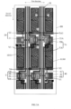
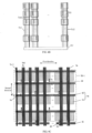
- FIG. 2A is a schematic top view of the array substrate provided by at least one embodiment of the present disclosure
- FIGs. 2B to 2D are schematic top views of some structures shown in FIG. 2A
- FIG. 2B shows a common electrode layer 10 and a first conductive layer 20 in FIG. 2A
- FIG. 2C shows the common electrode layer 10, the first conductive layer 20 and a second conductive layer 40 in FIG. 2A
- FIG. 2D shows the common electrode layer 10, the first conductive layer 20, the second conductive layer 40 and a third conductive layer 50 in FIG. 2A
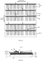
- FIG. 3A is a simplified sectional schematic view taken along the line I-I in FIG. 2A
- FIG. 3B is a simplified sectional schematic view taken along line II-II in FIG. 2A .
- the array substrate provided by at least one embodiment of the present disclosure includes a base substrate BS and a plurality of first signal lines 21 and a plurality of second signal lines 41 which are provided on the base substrate BS.
- the plurality of first signal lines 21 are provided in the first conductive layer 20, extend along a first direction, and are sequentially arranged along a second direction different from the first direction.
- the plurality of second signal lines 41 are provided in the second conductive layer 40, extend along the second direction and are sequentially arranged along the first direction. Orthographic projections of the second signal lines 41 on the base substrate BS intersect with orthographic projections of the first signal lines 21 on the base substrate BS.
- the first signal line 21 has a first width at a position where the first signal line 21 overlaps with the second signal line 41 and a second width at a position between the second signal lines 41 adjacent to each other (that is, at a position where the first signal line 21 does not overlap with the second signal line 41), the first width and the second width are dimensions of the first signal line 21 in the second direction, and the first width is smaller than the second width.
- the first signal line 21 is a gate line and the second signal line 41 is a data line.
- the first conductive layer 20 in which the first signal line 21 is provided and the second conductive layer 40 in which the second signal line 41 is provided are separated from each other by a gate insulating layer GI.
- the first signal line 21 is the data line and the second signal line 41 is the gate line.
- a region defined by intersecting the first signal lines 21 adjacent to each other and the second signal lines 41 adjacent to each other is a sub-pixel region, and the sub-pixel region includes an opening region and a non-opening region surrounding the opening region.
- the non-opening region is a region shielded by a black matrix, and the opening region is a region not shielded by the black matrix.
- the first signal lines 21 adjacent to each other and the second signal lines 41 adjacent to each other are provided in the non-opening region.
- the array substrate provided by at least one embodiment of the present disclosure is an array substrate used for realizing a display function.
- the sub-pixel region includes a display region (the opening region is the display region) and a non-display region surrounding the display region (the non-opening region is the non-display region), and the first signal lines 21 adjacent to each other and the second signal lines 41 adjacent to each other are provided in the non-display region of the sub-pixel region.
- the array substrate provided by the embodiments of the present disclosure may be an array substrate used for realizing other functions, which is not limited by the embodiments of the present disclosure. In the following embodiments, the array substrate is used to realize the display function as an example.
- the array substrate provided by at least one embodiment of the present disclosure further includes a plurality of touch signal lines Tx extending along the extension direction (i.e., the second direction) of the second signal lines 41 and sequentially arranged along the extension direction (i.e., the first direction) of the first signal lines 21.
- the plurality of touch signal lines Tx are grouped into a plurality of touch signal line groups TxG, and each touch signal line group TxG includes two touch signal lines Tx adjacent to each other (i.e., there is no other touch signal line Tx between the two touch signal lines Tx adjacent to each other).
- orthographic projections of the two touch signal lines Tx adjacent to each other on the base substrate BS are provided on two sides of an orthographic projection of a same second signal line 41 on the base substrate BS (i.e., the orthographic projection of the second signal line 41 is provided between the orthographic projections of the two touch signal lines Tx adjacent to each other).
- the touch signal lines Tx are provided in the third conductive layer 50, which is different from the first conductive layer 20 in which the first signal lines 21 are provided and the second conductive layer 40 in which the second signal lines 41 are provided. For example, as shown in FIG.
- the third conductive layer 50 is provided on a side of the second conductive layer 40 away from the base substrate BS, that is, the second conductive layer 40 is provided between the base substrate BS and the third conductive layer 50 in the direction perpendicular to the base substrate BS, and the second conductive layer 40 is separated from the third conductive layer 50 by a first passivation insulating layer PVX1, and the third conductive layer 50 is covered by a second passivation insulating layer PVX2.
- FIGs. 2A and 2D only shows two touch signal line groups TxG and two second signal lines 41 respectively corresponding to the two touch signal line groups TxG as an example.
- the orthographic projection of each second signal line 41 is provided between the orthographic projections of two touch signal lines adjacent to each other Tx included in a same touch signal line group TXG.
- the orthographic projection of the second signal line 41 is provided between the orthographic projections of two touch signal lines Tx adjacent to the second signal line 41, a difference between the electric fields on two sides of the second signal line 41 can be reduced, which is beneficial to prevent the touch signal lines Tx from affecting the display effect of the display device using the array substrate.
- one of the three signal lines i.e.
- the second signal line 41 and the two touch signal lines adjacent to the second signal line 41 fails and needs to be repaired, as compared the case that the second signal line 41 and the two touch signal lines Tx adjacent to the second signal line 41 are provided in a same layer, it is possible to avoid short circuit among the three signal lines and facilitate repairing of the failed signal line by adopting the arrangement in which the third conductive layer 50 in which the two touch signal lines Tx adjacent to each other are provided is different from the second conductive layer 40 in which the second signal line 41 is provided.
- the third conductive layer 50 in which the two touch signal lines Tx adjacent to each other are provided is different from the second conductive layer 40 in which the second signal line 41 is provided, the distance between any of the orthographic projections of the two touch signal lines Tx adjacent to each other and the orthographic projection of the second signal line 41 can be set to be relatively small; in this case, by arranging the two touch signal lines Tx adjacent to each other and the same second signal line 41 in the non-opening region of the sub-pixel region, the aperture ratio of the array substrate can be improved.
- the array substrate provided by at least one embodiment of the present disclosure further includes touch electrodes 11 spaced apart from each other and provided on the base substrate BS.
- the touch electrodes 11 are also used as common electrodes in the array substrate, that is to say, the common electrodes included in the array substrate are multiplexed as the touch electrodes 11; the display function is realized by applying a common electrode signal to the common electrodes in the display period, and the touch function is realized by applying a touch signal to the common electrodes in the touch period.
- the array substrate includes the common electrodes and pixel electrodes. For example, as shown in FIGs.
- the array substrate provided by at least one embodiment of the present disclosure includes the common electrodes (i.e., the touch electrodes 11) and the pixel electrodes 61 provided on the base substrate BS, the common electrodes are provided in a common electrode layer 10 and the pixel electrodes 61 are provided in a pixel electrode layer 60, that is, the common electrodes are provided in a layer different from the layer in which the pixel electrodes 61 are provided.
- the pixel electrode layer 60 is provided between the base substrate BS and the common electrode layer 10 in the direction perpendicular to the base substrate BS (as shown in FIGs. 6A to 7B ); in this case, each of the touch electrodes 11 in the common electrode layer farther from the base substrate BS has a plurality of slits that penetrate through the touch electrode 11.
- the common electrode layer 10 is provided between the base substrate BS and the pixel electrode layer 60 in the direction perpendicular to the base substrate BS; in this case, as shown in FIGs.
- each of the touch electrodes 11 has a solid structure without slits, and each of the pixel electrodes 61 has a plurality of slits ( FIGs. 2A to 2D illustrate that each pixel electrode has slits in two different directions to form a dual-domain structure as an example, and in other embodiments, each pixel electrode 61 may have a single domain or multiple-domain structure).
- each touch electrode 11 does not have the slit, each touch electrode 11 has a larger area, which is beneficial to enhance the touch performance.
- the touch electrode 11 is closer to the base substrate BS and has the larger area, a double-sided touch mode can be realized.
- a touch object e.g., a user's finger
- each sub-pixel region is a region defined by adjacent first signal lines 21 and adjacent second signal lines 41
- each sub-pixel region is provided with one touch electrode 11
- each touch electrode 11 is provided in one sub-pixel region. That is to say, the plurality of sub-pixel regions and the plurality of touch electrodes 1 1 in the array substrate are provided in one-to-one correspondence manner.
- one second signal line 41 is provided between touch electrodes adjacent to each other 11 in the first direction (i.e. the extension direction of the first signal line 21). It should be noted that in FIGs.
- the touch electrodes 11 are closer to the base substrate BS than the pixel electrodes 61.
- the touch electrodes 11 and the sub-pixel regions are also provided in a one-to-one correspondence manner to reduce the overlapping area between the touch electrodes 11 and the second signal lines 41, thereby reducing the load of the array substrate.
- each of the orthographic projections of the two touch signal lines Tx adjacent to each other included in the same touch signal line group TxG and the orthographic projection of the second signal line 41 provided between the two touch signal lines Tx adjacent to each other includes the portion provided between the orthographic projections of the touch electrodes 11 adjacent to each other on the base substrate BS.
- each of the orthographic projections of the two touch signal lines Tx adjacent to each other and the orthographic projection of the second signal line 41 provided between the two touch signal lines Tx adjacent to each other includes the portion provided between the orthographic projections of the touch electrodes 11 adjacent to each other on the base substrate BS
- an entirety or a part of the orthographic projection of any one of the three signal lines i.e. the two touch signal lines Tx adjacent to each other and the second signal line 41 provided between the two touch signal lines Tx adjacent to each other ) does not overlap with the touch electrodes 11. For example, as shown in FIGs.
- each touch signal line Tx includes a plurality of main portions TA and a plurality of bent portions TB, the plurality of main portions TA and the plurality of bent portions TB are alternately provided; the orthographic projection of each main portion TA on the base substrate BS is provided in the region between the orthographic projections of the touch electrodes11 adjacent to each other in the first direction on the base substrate BS.
- the main portion TA of each of the adjacent touch signal lines Tx and the second signal line 41 provided between the main portions TA of the adjacent touch signal lines Tx are provided between the touch electrodes 11 adjacent to each other in the first direction.
- the load of the array substrate can be effectively reduced.
- the orthogonal projection of the main portion TA does not overlap with the orthogonal projection of the touch electrode 11
- the orthogonal projection of the bent portion TB does not overlap with the orthogonal projection of the touch electrode 11, that is, the entirety of the orthogonal projection of the touch signal line Tx is provided in the region between the orthogonal projections of touch electrodes 11 adjacent to each other.
- the first signal line 21 has the above-mentioned first width at a position where the main portion TA of the touch signal line Tx overlaps with the first signal line 21.
- the load of the array substrate can be further reduced by designing the first signal line 21 to have a smaller width at the position where the main portion TA of the touch signal line Tx overlaps with the first signal line 21.
- the orthographic projection of the touch signal line Tx on the base substrate BS overlaps with or does not overlap with the orthographic projection of the pixel electrode 61 on the base substrate BS.
- the orthographic projection of the main portion TA of the touch signal line Tx does not overlap with the orthographic projection of the pixel electrode 61
- the orthographic projection of the bent portion TB of the touch signal line Tx overlaps with the orthographic projection of the pixel electrode 61.
- the orthographic projections of the main portion TA and the bent portion TB of the touch signal line Tx both overlap the orthographic projection of the pixel electrode 61, so as to increase the pixel capacitance and thus improve the pixel charging efficiency.
- the bent portion TB included in the touch signal line Tx is used to avoid the touch signal line Tx from overlapping with the switching elements included in the array substrate, thereby further reducing the load of the array substrate.
- the array substrate provided by at least one embodiment of the present disclosure includes a plurality of switching elements T provided on the base substrate BS, each switching element T is provided in a region between the bent portion TB and the second signal line 41 closest to the bent portion TB, and the switching element T is electrically connected with the pixel electrode 61.
- the switching element is a transistor, which includes a gate electrode GE, an active layer AL, a source electrode SE and a drain electrode DE, and the drain electrode DE is electrically connected to the pixel electrode 61 (for example, the drain electrode DE is electrically connected to the pixel electrode 61 through a via hole V5).
- the gate electrode GE is a part of the first signal line 21
- the source electrode SE is directly electrically connected with the second signal line 41
- the source electrode SE and the drain electrode DE are provided in a same conductive layer, which can simplify the manufacturing process of the array substrate.
- the first signal line 21 comprises a plurality of openings 21A, and the orthographic projections of some of the openings 21A on the base substrate BS respectively overlap with the orthographic projections of the bent portions TB on the base substrate BS.
- the opening 21A is an opening penetrating through the first signal line 21.
- the orthographic projections of some of the openings 21A respectively overlap with the orthographic projections of the bent portions TB on the base substrate BS respectively overlap with the orthographic projections of second extension portions 42 mentioned below (as shown in FIGs. 2A and 6A ) on the base substrate BS to further reduce the load.
- the orthographic projections of third extension portions 43 mentioned below on the base substrate BS respectively overlap with the orthographic projections of still another of the openings 21A on the base substrate BS to further reduce the load.
- the plurality of touch electrodes 11 in the array substrate are grouped into a plurality of touch sensing blocks, the touch electrodes 11 in each touch sensing block are electrically connected with each other, and each touch sensing block is electrically connected with one touch signal line Tx.
- FIG. 4A is a schematic view of an electrical connection relationship between the plurality of touch sensing blocks and the plurality of touch signal lines in the array substrate according to at least one embodiment of the present disclosure, and each black dot in FIG. 4A represents a via hole for electrical connection;
- FIG. 4B is another schematic view of the electrical connection relationship between the plurality of touch sensing blocks and the plurality of touch signal lines in the array substrate according to at least one embodiment of the present disclosure;
- FIG. 4C is a schematic view of a positional relationship between a single touch sensing block and some of the touch signal lines in the array substrate according to at least one embodiment of the present disclosure;
- FIG. 4A is a schematic view of an electrical connection relationship between the plurality of touch sensing blocks and the plurality of touch signal lines in the array substrate according to at least one embodiment of the present disclosure, and each black dot in FIG. 4A represents a via hole for electrical connection
- FIG. 4B is another schematic view of the electrical connection relationship between the plurality of touch sensing blocks and the plurality of
- FIG. 4D is a schematic top view of the plurality of touch sensing blocks in the array substrate provided by at least one embodiment of the present disclosure, and the embodiment shown in FIG. 4D shows two rows and two columns of touch sensing blocks TS for illustration;
- FIG. 4E is a partially enlarged schematic view of FIG. 4D .
- the array substrate provided by at least one embodiment of the present disclosure includes the plurality of touch sensing blocks TS provided on the base substrate and spaced apart from each other, each touch sensing block TS includes the touch electrodes 11 electrically connected to each other and spaced apart from each other, and each touch sensing block TS is electrically connected with one touch signal line Tx so that each touch sensing block TS is electrically connected with a touch control circuit TC by the one touch signal line Tx.
- the array substrate provided by at least one embodiment of the present disclosure adopts the self-capacitance principle to realize touch control, that is, each touch sensing block TS serves as a self-capacitance electrode, and the touch control circuit TC determines the touch position by detecting the change of the self-capacitance of the touch sensing block TS.
- each touch sensing block TS is electrically connected to only one touch signal line Tx, and each touch signal line is electrically connected to only one touch sensing block TS. That is, the plurality of touch sensing blocks TS in the array substrate are electrically connected with the plurality of touch signal lines Tx in one-to-one correspondence manner. It should be noted that the electrical connection relationship between the touch sensing blocks TS and the touch signal lines Tx is not limited to the manner shown in FIG. 4A . For example, in some embodiments, as shown in FIG. 4B , the total number of the touch signal lines Tx is greater than the total number of the touch sensing blocks TS in the array substrate.
- the plurality of touch signal lines Tx in the array substrate include a plurality of first touch signal lines Tx1 and a plurality of second touch signal lines Tx2, the plurality of first touch signal lines Tx1 and the plurality of second touch signal lines Tx2 are electrically connected with the touch control circuit TC and are applied with the same touch signal during operation, the plurality of first touch signal lines Tx1 are respectively electrically connected with the plurality of touch sensing blocks TS, and the plurality of second touch signal lines Tx2 are insulated from the plurality of touch sensing blocks TS.
- each second signal line 41 is provided between two touch signal lines Tx adjacent to each other, so that in the case that the total number of the second signal lines 41 is relatively large, the total number of the touch signal lines Tx that need to be provided is also relatively large. If the total number of the touch signal lines Tx is set to be equal to the total number of the touch sensing blocks TS, then there exists a case that a part of the second signal lines 41 are not provided between the two touch signal lines Tx adjacent to each other.
- the second touch signal lines Tx2 electrically insulated from any one of the touch sensing blocks TS are provided, so that the total number of the touch signal lines Tx is larger than the total number of the touch sensing blocks TS, and each second signal line 41 is provided between two touch signal lines Tx adjacent to each other.
- first touch signal line Tx1 and the second signal line Tx2 have the same width in the first direction.
- multiple touch signal line groups TxG (for example, each touch signal line group TxG is provided in a gap between two touch electrodes adjacent to each other 11) pass through a region in which the touch sensing block TS-1 is provided, one touch signal line Tx (see Tx-1 in FIG. 4C ) of the multiple touch signal line groups TxG is electrically connected with the touch sensing block TS-1, and the other touch signal lines Tx of the multiple touch signal line groups TxG are insulated from the touch sensing block TS-1.
- the touch signal line Tx-1 is electrically connected to a plurality of first extension portions 22 included in the touch sensing block TS-1 (the arrangement manner of the first extension portions 22 will be described in detail below).
- the first extension portions 22 are electrically connected to the same touch signal line Tx-1 through via holes V4 (see FIGs. 4C and 2A ).
- the touch signal line Tx see Tx-1
- the signal transmission speed can be increased, and the occurrence probability of poor electrical connection between the touch signal line Tx and the touch sensing block TS can be reduced.
- the electrical connection between the touch sensing block TS and its corresponding touch signal line Tx is not limited to the manner shown in FIG. 4C , as long as the electrical connection between the touch sensing block TS and its corresponding touch signal line Tx can be realized.
- FIG. 4C only exemplarily shows one touch sensing block TS and the multiple touch signal lines Tx passing through the touch sensing block, but does not show the second signal line between the two touch signal lines Tx adjacent to each other included in the same touch signal line group TxG.
- each touch sensing block TS includes a plurality of touch electrode groups TG arranged sequentially, and each touch electrode group TG includes a plurality of touch electrodes 11 spaced apart from each other and a first extension portion 22 electrically connected with the plurality of touch electrodes 11.
- the first extension 22 is directly electrically connected with the touch electrode 11 (i.e., the electrical connection therebetween is not realized by a via hole or a relay conductive element).
- the electrical connection therebetween is not realized by a via hole or a relay conductive element.
- each touch sensing block TS further includes a plurality of second extension portions 42, and each second extension portion 42 is provided between and electrically connected to touch electrode groups TG adjacent to each other.
- each second extension portion 42 extends in the second direction, and each second extension portion 42 is electrically connected with two touch electrode groups TG adjacent to each other through a first via hole V1 and a second via hole V2 (see FIGs. 4C-4E and 2A ), respectively.
- the touch electrode groups TG adjacent to each other are electrically connected with each other by at least two second extension portions 42, which can improve the signal transmission speed.
- at most every six sub-pixel regions corresponds to one second extension portion 42.
- every four sub-pixel regions correspond to one second extension portion 42 in the first direction.
- each touch sensing block TS includes the touch electrodes 11 spaced apart from each other and at least a portion of the touch signal line Tx and at least a portion of the second signal line 41 are provided in a region between two touch electrodes adjacent to each other 11, the load of the array substrate can be effectively reduced.
- the touch sensing block TS is obtained by electrically connecting the plurality of touch electrodes 11 spaced apart from each other by using the first extension portions 22 and the second extension portions 42, so that the touch sensing block TS has a grid-like structure, and thus the resistance of the touch sensing block TS is small.
- each of the first extension portion 22 and the second extension portion 42 is provided in the non-opening region of the array substrate to improve the aperture ratio of the array substrate.
- the first extension portion 22 has a first width at positions where the first extension portion 22 respectively overlaps with the second signal line 41 and the touch signal lines Tx, and has a second width between adjacent second signal lines 41, the first width and the second width are dimensions of the first extension portion 22 in the second direction, and the first width is smaller than the second width.
- the first extension portion 22 have a smaller width at positions where the first extension portion 22 respectively overlaps with the second signal line 41 and the touch signal line Tx, so that the load of the array substrate is further reduced.
- the orthographic projection of the second extension portion 42 on the base substrate overlaps with the opening 21A in the first signal line 21 to further reduce the load of the array substrate.
- the first extension portion 22 and the first signal line 21 are provided in a same layer (see the first conductive layer 20), that is, the first extension portion 22 and the first signal line 21 are formed by patterning a same film with a same mask, which can simplify the manufacturing process of the array substrate.
- the second extension portion 42 and the second signal line 41 are provided in a same layer (see the second conductive layer 40), that is, the second extension portion 42 and the second signal line 41 are formed by patterning a same film with a same mask, which can simplify the manufacturing process of the array substrate.
- one first signal line 21 is provided between the touch electrode groups TG adjacent to each other included in the same touch sensing block TS, and one first signal line 21 is provided between the touch sensing blocks TS adjacent to each other in the second direction (that is, the extension direction of the second signal line 41).
- FIG. 4C does not show the first signal line 21 provided between the touch electrode groups TG adjacent to each other included in the same touch sensing block TS, but only shows one touch sensing block TS and one first signal line 21 provided between the touch sensing blocks TS adjacent to each other.
- the first signal line 21 is not shown in FIGs. 4D and 4E .
- a third extension portion 43 is provided between the touch sensing blocks TS-1 and TS-2 adjacent to each other in the second direction, and the third extension portion 43 is electrically connected with one of the touch sensing blocks TS-1 and TS-2 adjacent to each other and is electrically insulated from the other of the touch sensing blocks TS-1 and TS-2 adjacent to each other.
- the third extension portion 43 is electrically connected with the touch sensing block TS-2 (see FIGs. 4D and 4E ) for example by a third via hole V3, and the third extension portion 43 is electrically insulated from the touch sensing block TS-1.
- FIG. 4D and 4E the third extension portion 43 is electrically insulated from the touch sensing block TS-1.
- one first signal line 21 is provided between the touch sensing blocks TS-1 and TS-2 adjacent to each other in the second direction ( FIG. 4C only shows the touch sensing block TS-1), the orthographic projection of the third extension portion 43 provided between the touch sensing blocks TS-1 and TS-2 adjacent to each other on the base substrate BS overlaps with the orthographic projection of the first signal line 21 provided between the touch sensing blocks TS-1 and TS-2 adjacent to each other on the base substrate
- the first extension portions 22 of the touch sensing blocks TS adjacent to each other in the first direction are disconnected from each other (for example, the distance between the first extension portions 22 of the touch sensing blocks TS adjacent to each other in the first direction is greater than or equal to 5 microns), so that the touch sensing blocks TS adjacent to each other are electrically insulated from each other in the first direction; in addition, the touch sensing blocks TS adjacent to each other in the second direction are electrically insulated from each other because of the third extension portion 43.
- one first signal line 21 is provided between the touch electrode groups TG adjacent to each other in the same touch sensing block TS, so that the orthographic projection of the second extension portion 42 electrically connecting the touch electrode groups TG adjacent to each other on the base substrate BS overlaps with the orthographic projection of the first signal line 21 on the base substrate BS;
- the third extension portion 43 is provided between the touch sensing blocks TS-1 and TS-2 adjacent to each other, the third extension portion 43 is electrically connected with the touch sensing block TS-2 and electrically insulated from the touch sensing block TS-1, and the third extension portion 43 overlaps with the first signal line 21 provided between the touch sensing blocks TS-1 and TS-2 adjacent to each other, so that the first signal line 21 provided between touch electrode groups TG adjacent to each other of the same touch sensing block TS and the first signal line 21 provided between the touch sensing blocks TS-1 and TS-2 adjacent to each other have parasitic capacitances substantially equal to each other, and the uniformity of the parasitic capacitances of the first signal
- the total number of the second extension portions 42 provided between the touch electrode groups TG adjacent to each other of the same touch sensing block TS is equal to the total number of the third extension portions 43 provided between the touch sensing blocks TS-1 and TS-2 adjacent to each other in the second direction.
- the second extension portion 42 and the third extension portion 43 are provided in a same layer to simplify the manufacturing process of the array substrate, and the second extension portion 42 and the third extension portion 43 extend along the extension direction of the second signal line 41.
- the plurality of openings 21A are provided in each of the plurality of first signal lines 21 of the array substrate; the orthographic projection of the second extension portion 42 on the base substrate BS overlaps with the orthographic projection of the opening 21A on the base substrate BS.
- FIG. 2A only shows the manner in which the second extension portion 42 overlaps with the opening 21A.
- the orthogonal projection of the third extension portion 43 on the base substrate BS overlaps with the orthogonal projection of the opening 21A on the base substrate BS, and the way in which the third extension portion 43 overlaps with the opening 21A is similar to the way in which the second extension portion 42 overlaps with the opening 21A.
- the third extension portion 43 is provided in the second conductive layer 40, that is, the third extension portion 43, the second extension portion 42, and the second signal line 41 are provided in the same layer (see the second conductive layer 40), so that the third extension portion 43, the second extension portion 42, and the second signal line 41 are formed by patterning the same film using the same mask plate, which can simplify the manufacturing process of the array substrate.
- each of the second extension portion 42 and the third extension portion 43 extends along the extension direction of the second signal line 41 (i.e., the second direction) to simplify the wiring.
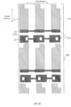
- FIG. 5A is a schematic sectional view taken along the line A-A' in FIG. 4C ;
- FIG. 5B is a schematic sectional view taken along the line B-B' in FIG. 4C , and FIG. 5B does not show the second signal line 41 between the touch signal lines Tx adjacent to each other;
- FIG. 5C is a schematic sectional view taken along the line C-C' in FIG. 4E ;
- FIG. 5D is a schematic sectional view taken along the line D-D' in FIG. 4E .
- the common electrode layer 10 the first conductive layer 20, the gate insulating layer GI, the active layer AL, the second conductive layer 40, the first passivation insulating layer PVX1, the third conductive layer 50, the second passivation insulating layer PVX2 and the pixel electrode layer 60 are sequentially provided on the base substrate BS from bottom to top as an example.
- the material of the pixel electrode layer 60 are used to realize electrical connection at the via holes V1-V4.
- the pixel electrode layer 60 includes a first portion 6A, a second portion 6B, a third portion 6C and a fourth portion 6d. As shown in FIGs.
- the first portion 6A is provided in the first via hole V1 to electrically connect the second extension portion 42 with the touch electrode 11 in one touch electrode group TG; as shown in FIGs. 4E and 5C , the second portion 6B is provided in the second via hole V2 to electrically connect the second extension portion 42 with the touch electrode 11 in the other touch electrode group TG; as shown in FIG. 4E and FIG. 5D , the third portion 6C is provided in the third via hole V3 to electrically connect the third extension portion 43 with the first extension portion 22 in the touch sensing block TS, thereby electrically connecting the third extension portion 43 with the touch sensing block TS; as shown in FIG.
- the fourth portion 6D is provided in the fourth via hole V4 to electrically connect the touch signal line Tx with the corresponding first extension portion 22, thereby realizing the electrical connection between the touch sensing block TS and the corresponding touch signal line Tx.
- the array substrate shown in FIG. 2A can be manufactured by the following steps.
- the common electrode layer 10 includes a plurality of rows of touch electrodes 11 spaced apart from each other (the row direction is along the first direction), and the plurality of rows of touch electrodes 11 extend along the first direction and are sequentially arranged along the second direction.
- Step S12 as shown in FIG. 2B , forming a first conductive layer 20 on the base substrate BS by using a first conductive layer mask.
- the first conductive layer 20 includes a plurality of first signal lines 21 extending along the first direction and a plurality of rows of first extension portions 22 extending along the first direction.
- Each row of first extension portions 22 includes a plurality of first extension portions 22 disconnected from each other, and each first extension portion 22 is electrically connected with some touch electrodes 11 of the same row of touch electrodes 11 to constitute the touch electrode group TG.
- the touch electrodes 11 and a row of first extension portions 22 corresponding to the touch electrodes 11 form a plurality of touch electrode groups TG arranged sequentially along the first direction; and in the second direction, a plurality of first signal lines 21 and a plurality of rows of first extension portions 22 are alternately provided and electrically insulated from each other.
- S14 forming a plurality of active layers AL (as shown in FIG. 2A ) by using an active layer mask on the base substrate BS on which gate insulating initial film is formed.
- Step S15 as shown in FIG. 2C , forming a second conductive layer 40 on the base substrate BS by using a second conductive layer mask.
- the second conductive layer 40 includes a plurality of source electrodes SE and a plurality of drain electrodes DE, and the source electrodes SE, the drain electrodes DE, the active layers AL, and a portion (which serves as gate electrodes) of the first signal lines 21 form a plurality of switching elements T.
- the second conductive layer 40 further includes a plurality of second signal lines 41 extending along the second direction and a plurality of columns of extension portions extending along the second direction. As shown in FIG.
- the plurality of columns of extension portions include a plurality of second extension portions 42 disconnected from each other and a plurality of third extension portions 43 disconnected from each other.
- One row of touch electrodes 11 is provided between the second extension portions adjacent to each other 42 in the second direction, each second extension portion 42 electrically connects the touch electrode groups TG adjacent to each other in the second direction.
- Multiple rows of touch electrodes 11 are provided between the third extension portions 43 adjacent to each other in the second direction, and each third extension portion 43 is electrically connected to only one touch electrode group TG of the touch electrode groups TG adjacent to each other.
- each touch sensing block TS includes a plurality of touch electrode groups TG which are electrically connected with each other and arranged sequentially in the second direction
- Step S17 forming a third conductive layer 50 on the base substrate BS on which the first passivation insulating initial film is formed by using a third conductive layer mask.
- the third conductive layer 50 includes a plurality of touch signal lines Tx.
- the via hole V4 penetrates the gate insulating layer GI, the first passivation insulating layer PVX1 and the second passivation insulating layer PVX2.
- the via hole V5 penetrates through the first passivation insulating layer PVX1 and the second passivation insulating layer PVX2 to expose a part of the drain electrode DE (as shown in FIGs. 2A and 2D ).
- Step S19 as shown in FIG. 2A , forming a pixel electrode layer 60 on the base substrate BS by using a pixel electrode layer mask.
- the pixel electrode layer 60 includes a plurality of pixel electrodes 61, a plurality of first portions 6A, a plurality of second portions 6B, a plurality of third portions 6C and a plurality of fourth portions 6D.
- the pixel electrode 61 extends into the via hole V5 to electrically connect with the drain electrode DE.
- FIGs. 1 As shown in FIGs.
- the first portion 6A extends into the first via hole V1 to electrically connect the second extension portion 42 with the touch electrode 11 of one touch electrode group TG.
- the second portion 6B extends into the second via hole V2 to electrically connect the second extension portion 42 with the touch electrode 11 of the other touch electrode group TG.
- the third portion 6C extends into the third via hole V3 to electrically connect the third extension portion 43 with the first extension portion 22 of the touch sensing block TS, thereby electrically connecting the third extension portion 43 with the touch sensing block TS.
- the fourth portion 6D extends into the fourth via hole V4 to electrically connect the touch signal line Tx with the corresponding first extension portion 22.
- the embodiments of the present disclosure do not limit the sequence of the above steps.
- the step S11 may be performed after the step S12.
- the pixel electrode layer 60 may be formed first, and the common electrode layer 10 may be formed later.
- each of the common electrode layer 10 and the pixel electrode layer 60 is made of a transparent conductive metal oxide such as indium tin oxide or indium zinc oxide.
- each of the first conductive layer 20, the second conductive layer 40 and the third conductive layer 50 is made of a metal material such as aluminum, aluminum alloy, copper, copper alloy, molybdenum or nickel.
- each of the first conductive layer 20, the second conductive layer 40, and the third conductive layer 50 has a single-layer structure or a multi-layer structure.
- each of the gate insulating layer GI, the first passivation insulating layer PVX1 and the second passivation insulating layer PVX2 is made of an inorganic insulating material, such as silicon dioxide, silicon nitride or silicon oxynitride.
- FIG. 6A is another schematic top view of the array substrate provided by at least one embodiment of the present disclosure
- FIG. 6B is a schematic plan view of some structures in FIG. 6A
- FIG. 7A is a simplified sectional schematic view taken along the line III-III in FIG. 6A
- FIG. 7B is a simplified sectional schematic view taken along line IV-IV in FIG. 6A .
- the array substrate provided by at least one embodiment of the present disclosure includes a common electrode layer 10 and a pixel electrode layer 60, and the pixel electrode layer 60 is provided between the base substrate and the common electrode layer 10 in the direction perpendicular to the base substrate.
- the common electrode layer 10 includes the touch electrodes 11, and the second extension portions 42 and the third extension portions 43 extending in the same direction.
- the first extension portions 22 and the touch electrodes 11, the second extension portions 42 and the third extension portions 43 included in the common electrode layer 10 are combined to form a plurality of touch sensing blocks TS.
- the touch electrodes 11 adjacent to each other in the second direction are electrically connected with each other by the second extension portion 42, the second extension portion 42 is directly connected to the touch electrodes 11 adjacent to each other in the second direction; the touch electrodes 11 adjacent to each other in the first direction are electrically connected with each other through the first extension portion 22 (for example, the touch electrode 11 extends into the via hole V6 to electrically connect the corresponding first extension portion 22, as shown in FIGs. 6A and 7B ); and thus, the touch electrodes 11 in the same touch sensing block TS are connected with each other.
- the manner of disconnection between the touch sensing blocks TS adjacent to each other in the first direction is similar to the manner shown in FIG.
- the disconnection between the touch sensing blocks TS adjacent to each other in the first direction is realized by disconnecting the first extension portions 22 of the adjacent touch sensing blocks TS from each other.
- the touch sensing blocks TS (see TS-1 and TS-2) adjacent to each other in the second direction are electrically insulated from each other by the third extension portion 43.
- the third extension portion 43 is directly connected with the touch electrode 11 of the touch sensing block TS-2, protrudes from the touch electrode 11 of the touch sensing block TS-2 in the second direction and then passes over the first signal line 21, but does not extend to the touch electrode 11 of the touch sensing block TS-1
- the first extension portion 22 and the first signal line 21 are provided in the same layer, that is, they are provided in the first conductive layer 20, so as to simplify the manufacturing process of the array substrate.
- the third extension portion 43 overlaps with the opening 21A of the first signal line 21 to reduce the load of the array substrate.
- the array substrate shown in FIGs. 6A to 7B is manufactured by the following steps.
- the pixel electrode layer 60 includes a plurality of pixel electrodes 61.
- the first conductive layer 20 includes a plurality of first signal lines 21 and a plurality of rows of first extension portions 22, the plurality of first signal lines 21 and the plurality of rows of first extension portions 22 extend along the first direction and are arranged sequentially along the second direction different from the first direction.
- Each row of first extension portions 22 includes a plurality of first extension portions 22 disconnected from each other.
- the plurality of first signal lines 21 and the plurality of rows of first extension portions 22 are alternately provided and insulated from each other.
- the second conductive layer 40 includes a plurality of second signal lines 41 extending along the second direction, source electrodes SE and drain electrodes DE.
- a portion (which serves as gate electrodes GE) of the first signal lines 21, the active layers AL, the source electrodes SE and drain electrodes DE are combined form the switching elements T.
- the third conductive layer 50 includes a plurality of touch signal lines, and each touch signal line is electrically connected with the first extension portions 22 of the plurality of touch electrode groups included in the same touch sensing block.
- S28 forming a second passivation insulating initial film used for forming a second passivation insulating layer PVX2 on the base substrate BS to cover the third conductive layer 50, and patterning the gate insulating initial film, the first passivation insulating initial film and the second passivation insulating initial film by using an insulating layer mask to form the gate insulating layer GI, the first passivation insulating layer PVX1, the second passivation insulating layer PVX2 and via holes V4-V6.
- the via holes V4 and V6 penetrate through the gate insulating layer GI, the first passivation insulating layer PVX1 and the second passivation insulating layer PVX2 to expose a part of the surface of the first extension portion 22, and the via hole V5 penetrates through the gate insulating layer GI, the first passivation insulating layer PVX1 and the second passivation insulating layer PVX2 to expose a part of the surface of the pixel electrode 61.
- the common electrode layer 10 includes the touch electrodes 11, the second extension portions 42 and the third extension portions 43.
- the touch electrode 11 extends into the via hole V6 to electrically connect the corresponding first extension portion 22, so as to realize the electrical connection between the touch electrodes 11 adjacent to each other 11 in the first direction.
- the second extension portion 42 electrically connects the touch electrodes 11 adjacent to each other in the second direction.
- the third extension portion 43 is electrically connected to only one touch electrode 11.
- the touch electrodes 11, the second extension portions 42 and the third extension portions 43 included in the common electrode layer 10 and the plurality of rows of first extension portions 22 included in the first conductive layer 20 are combined to form a plurality of touch sensing blocks TS.
- the touch electrode 11 extends into the via hole V4 to electrically connect the touch signal line Tx with the first extension portion 22.
- a part of the material of the common electrode layer 10 is filled into the via hole V5 to electrically connect the drain electrode DE with the corresponding pixel electrode 61.
- the arrangement manner of the touch signal lines Tx, the first signal lines 21 and the second signal lines 41, the amount relationship and electrical connection relationship between the touch signal lines Tx and the touch sensing blocks TS, and the positional relationship between the touch electrodes 11 and the sub-pixel regions are respectively same as those shown in FIGs. 2A to 5D , which will not be repeated for simplicity.
- At least one embodiment of the present disclosure further provides a touch display device, which comprises the array substrate provided by any one of the above embodiments.
- the touch display device provided by at least one embodiment of the present disclosure is an in-cell touch display device.
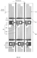
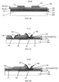
- FIG. 8A is a simplified sectional schematic view taken along the line I-I in FIG. 2A in the case that the touch display device provided by at least one embodiment of the present disclosure is the in-cell touch display device
- FIG. 8B is a simplified sectional schematic view taken along the line II-II in FIG. 2A in the case that the touch display device provided by at least one embodiment of the present disclosure is the in-cell touch display device.
- the in-cell touch display device includes an array substrate 1 and an opposite substrate 2 provided opposite to the array substrate 1; and the array substrate is the array substrate provided by any one of the above embodiments.
- the touch electrodes 11 of the array substrate 1 are provided on a side of the array substrate 1 facing the opposite substrate 2, and the opposite substrate 2 includes a base substrate BS2 and a black matrix BM.
- the first signal lines 21, the second signal lines 41 and the touch signal lines Tx are all shielded by the black matrix BM, that is, the first signal lines 21, the second signal lines 41 and the touch signal lines Tx are all provided in the non-opening region of the sub-pixel region.
- the first extension portions 22 are also shielded by the black matrix BM.
- the in-cell touch display device is a liquid crystal display device; in this case, a liquid crystal layer is provided between the array substrate 1 and the opposite substrate 2, and the pixel electrodes 61 and the common electrodes (which are also served as the touch electrodes 11) included in the array substrate 1 are used to generate an electric field for controlling the deflection of liquid crystal molecules in the liquid crystal layer.
- the touch display device is not the in-cell touch display device.
- the touch electrodes 11 are closer to the base substrate BS than the pixel electrodes 61, so the touch display device is capable of realizing the double-sided touch mode. That is, in the front touch mode, a touch object (e.g., a user's finger) touches the side of the display device provided with the opposite substrate 2; in the back touch mode, the touch object touches the side of the display device provided with the array substrate 1.
- a touch object e.g., a user's finger
- the touch object touches the side of the display device provided with the array substrate 1.
- the positions of the touch electrode 11 and the pixel electrode 61 may be interchanged.
- the touch display device is any product or component with touch and display functions, such as liquid crystal panel, electronic paper, OLED (Organic Light Emitting Diode) panel, mobile phone, tablet computer, television, display, notebook computer, digital photo frame, navigator, etc.
- OLED Organic Light Emitting Diode
- the manufacturing method includes: forming a plurality of first signal lines 21 on the base substrate BS; forming a plurality of second signal lines 41 on the base substrate BS, so that the orthographic projections of the second signal lines 41 on the base substrate BS intersect with the orthographic projections of the first signal lines 21 on the base substrate BS; forming a plurality of touch sensing blocks TS provided on the base substrate BS and spaced apart from each other, so that each touch sensing block TS includes a plurality of touch electrodes 11 electrically connected with each other and spaced apart from each other; and forming a plurality of touch signal lines Tx on the base substrate BS, so that at least some of the touch signal lines Tx are electrically connected with the touch sensing blocks TS respectively.
- the touch signal lines Tx are electrically connected to the touch sensing blocks TS in one-to-one correspondence manner; or, as shown in FIG. 4B , the first touch signal lines Tx1 are electrically connected with the touch sensing blocks TS in one-to-one correspondence manner, and the second touch signal lines Tx2 are electrically insulated from the touch sensing blocks TS. It should be noted that the electrical connection between the touch signal lines Tx and the touch sensing blocks TS is not limited to the manners shown in FIGs. 4A and 4B .
- the plurality of touch signal lines Tx extend along the extension direction of the plurality of second signal lines 41, the plurality of touch signal lines Tx are grouped into a plurality of touch signal line groups TG, each touch signal line group TG includes the touch signal lines Tx adjacent to each other, the orthographic projections of the touch signal lines Tx adjacent to each other included in the same touch signal line group TG are provided on two sides of the orthographic projection of the same second signal line 41 on the base substrate BS.
- Each of the orthographic projections of the touch signal lines Tx adjacent to each other and the orthographic projection of the same second signal line 41 includes a portion provided between the orthographic projections of the touch electrodes adjacent to each other 11 on the base substrate BS, and the layer 50 in which the touch signal lines Tx adjacent to each other are provided is different from the layer 40 in which the same second signal line 41 is provided. Because each of the touch signal line Tx and the second signal line 41 includes a portion that does not overlap with the touch electrode 11, the load of the array substrate can be reduced. Because the second signal line 41 is provided between the two touch signal lines Tx adjacent to each other included in the same touch signal line group TG, the uniformity of the electric fields on two sides of the second signal line 41 is improved. Because the touch signal line Tx and the second signal line 41 are provided in different layers, it is beneficial to improve the aperture ratio and facilitate the repairing of the signal line.
Landscapes
- Engineering & Computer Science (AREA)
- General Engineering & Computer Science (AREA)
- Theoretical Computer Science (AREA)
- Human Computer Interaction (AREA)
- Physics & Mathematics (AREA)
- General Physics & Mathematics (AREA)
- Computer Networks & Wireless Communication (AREA)
- Position Input By Displaying (AREA)
- Devices For Indicating Variable Information By Combining Individual Elements (AREA)
- Liquid Crystal (AREA)
Claims (15)
- Array-Substrat, mit:einem Basissubstrat (BS);einer Vielzahl von ersten Signalleitungen (21), die auf dem Basissubstrat (BS) bereitgestellt sind;einer Vielzahl von zweiten Signalleitungen (41), die auf dem Basissubstrat (BS) bereitgestellt sind, wobei sich die orthographischen Projektionen der Vielzahl von zweiten Signalleitungen (41) auf dem Basissubstrat (BS) mit den orthographischen Projektionen der Vielzahl von ersten Signalleitungen (21) auf dem Basissubstrat (BS) kreuzen;einer Vielzahl von Berührungserfassungsblöcken (TS), die auf dem Basissubstrat (BS) bereitgestellt und voneinander beabstandet sind, wobei jeder der Vielzahl von Berührungserfassungsblöcken (TS) eine Vielzahl von Berührungselektroden (11) aufweist, die elektrisch miteinander verbunden und voneinander beabstandet sind; undeiner Vielzahl von Berührungssignalleitungen (Tx), die auf dem Basissubstrat (BS) bereitgestellt sind, wobei zumindest einige der Vielzahl von Berührungssignalleitungen (Tx) jeweils mit der Vielzahl von Berührungserfassungsblöcken (TS) elektrisch verbunden sind, wobeidie Vielzahl von Berührungssignalleitungen (Tx) sich entlang einer Erstreckungsrichtung der Vielzahl von zweiten Signalleitungen (41) erstrecken, die Vielzahl von Berührungssignalleitungen (Tx) in eine Vielzahl von Berührungssignalleitungsgruppen (TxG) gruppiert sind, jede Berührungssignalleitungsgruppe (TxG) die Berührungssignalleitungen (Tx) nebeneinander aufweist, die orthographischen Projektionen der Berührungssignalleitungen (Tx), die einander benachbart sind und in einer gleichen Berührungssignalleitungsgruppe (TxG) auf dem Basissubstrat (BS) enthalten sind, jeweils auf zwei Seiten der orthographischen Projektion einer gleichen zweiten Signalleitung (41) auf dem Basissubstrat (BS) bereitgestellt werden, jede der orthographischen Projektionen der Berührungssignalleitungen (Tx), die einander benachbart sind, und die orthographische Projektion derselben zweiten Signalleitung (41) einen Abschnitt aufweist, der zwischen den orthographischen Projektionen der Berührungselektroden (11), die einander benachbart sind, auf dem Basissubstrat (BS) bereitgestellt ist, und eine Schicht, in der die Berührungssignalleitungen (Tx), die einander benachbart sind, bereitgestellt sind, sich von einer Schicht unterscheidet, in der dieselbe zweite Signalleitung (41) bereitgestellt ist;wobei jede der Vielzahl von Berührungssignalleitungen (Tx) eine Vielzahl von Hauptabschnitten (TA) und eine Vielzahl von gebogenen Abschnitten (TB) aufweist, und die Vielzahl von Hauptabschnitten (TA) und die Vielzahl von gebogenen Abschnitten (TB) abwechselnd bereitgestellt sind;dadurch gekennzeichnet, dass die orthographische Projektion jedes der Vielzahl von Hauptabschnitten (TA) auf dem Basissubstrat (BS) in einem Bereich zwischen den orthographischen Projektionen der Berührungs-Elektroden (11) nebeneinander auf dem Basissubstrat (BS) bereitgestellt ist.
- Array-Substrat nach Anspruch 1, das ferner eine Vielzahl von Schaltelementen (T) aufweist, die auf dem Basissubstrat (BS) bereitgestellt sind, wobei jedes der Vielzahl von Schaltelementen (T) zwischen einem der Vielzahl von gebogenen Abschnitten (TB) und derselben zweiten Signalleitung (41) bereitgestellt ist.
- Array-Substrat nach Anspruch 1 oder 2, wobeidie Vielzahl der ersten Signalleitungen (21) mit einer Vielzahl von Öffnungen (21A) bereitgestellt sind; unddie orthographischen Projektionen von mindestens einigen der Vielzahl von Öffnungen (21A) auf dem Basissubstrat (BS) sich jeweils mit den orthographischen Projektionen der Vielzahl von gebogenen Abschnitten (TB) auf dem Basissubstrat (BS) überlappen.
- Array-Substrat nach einem der Ansprüche 1-3, wobeijeder der Vielzahl von Berührungserfassungsblöcken (TS) eine Vielzahl von nacheinander angeordneten Berührungselektrodengruppen (TG) aufweist, und jede der Vielzahl von Berührungselektrodengruppen (TG) mehrere voneinander beabstandete Berührungselektroden (11) und einen ersten Verbindungsabschnitt (22) aufweist, der elektrisch mit den mehreren Berührungselektroden (11) verbunden ist; undjeder der Vielzahl von Berührungserfassungsblöcken (TS) ferner eine Vielzahl von zweiten Verbindungsabschnitten (42) aufweist, und jeder der Vielzahl von zweiten Verbindungsabschnitten (42) zwischen den Berührungselektrodengruppen (TG), die einander benachbart sind, bereitgestellt wird und mit diesen elektrisch verbunden ist.
- Array-Substrat nach Anspruch 4, wobeieine der Vielzahl von ersten Signalleitungen (21) und ein dritter Abschnitt (43) zwischen den Berührungserfassungsblöcken (TS), die einander in der Erstreckungsrichtung der Vielzahl von zweiten Signalleitungen (41) benachbart sind, bereitgestellt werden, der dritte Abschnitt (43) elektrisch mit einem der Berührungserfassungsblöcke (TS), die einander benachbart sind, verbunden und von den anderen der Berührungserfassungsblöcke (TS), die einander benachbart sind, isoliert ist, und die orthographische Projektion des dritten Erweiterungsabschnitts (43) auf dem Basis-Teil (BS) sich mit der orthographischen Projektion der einen der Vielzahl von ersten Signalleitungen (21) schneidet, die zwischen den Berührungserfassungsblöcken (TS), die einander benachbart sind, auf dem Basissubstrat (BS) bereitgestellt sind,vorzugsweise die Vielzahl von zweiten Erweiterungsabschnitten (42) und der dritte Erweiterungsabschnitt (43) in derselben Schicht bereitgestellt sind und die Vielzahl von zweiten Erweiterungsabschnitten (42) und der dritte Erweiterungsabschnitt (43) sich entlang der Erstreckungsrichtung der Vielzahl von zweiten Signalleitungen (41) erstrecken.
- Array-Substrat nach Anspruch 5, wobei die Vielzahl der ersten Signalleitungen (21) mit einer Vielzahl von Öffnungen (21A) bereitgestellt ist und die orthographischen Projektionen der Vielzahl der zweiten Leitungsabschnitte (42) und des dritten Leitungsabschnitts (43) auf dem Basissubstrat (BS) jeweils mit den orthographischen Projektionen von mindestens einigen der Vielzahl von Öffnungen (21A) auf dem Basissubstrat (BS) überlappen.
- Array-Substrat nach einem der Ansprüche 5-6, wobeidas Array-Substrat eine gemeinsame Elektrodenschicht (10) und eine Pixel-Elektrodenschicht (60) aufweist, die gemeinsame Elektrodenschicht (10) zwischen dem Basissubstrat (BS) und der Pixel-Elektrodenschicht (60) in einer Richtung senkrecht zum Basissubstrat (BS) bereitgestellt ist, und die gemeinsame Elektrodenschicht (10) die Vielzahl von Berührungselektroden (11) in der Vielzahl von Berührungserfassungsblöcken (TS) aufweist;die Pixel-Elektrodenschicht (60) einen ersten Abschnitt (6A), einen zweiten Abschnitt (6B) und einen dritten Abschnitt (6C) aufweist, wobei eine der Vielzahl von zweiten Erweiterungsabschnitten (42) mit den Berührungselektrodengruppen (TG), die einander benachbart sind, durch den ersten Abschnitt (6A) und den zweiten Abschnitt (6B) elektrisch verbunden ist, und der dritte Erweiterungsabschnitt (43) mit dem einen der Berührungserfassungsblöcke (TS), die einander benachbart sind, durch den dritten Abschnitt (6C) elektrisch verbunden ist.
- Array-Substrat nach Anspruch 7, wobeidie Pixel-Elektrodenschicht (60) ferner einen vierten Abschnitt (6D) aufweist und der erste Erweiterungsabschnitt (22) mit einer der Vielzahl von Berührungssignalleitungen (Tx) durch den vierten Abschnitt (6D) elektrisch verbunden ist, um den Berührungserfassungsblock (TS), der den ersten Erweiterungsabschnitt (22) aufweist, mit der einen der Vielzahl von Berührungssignalleitungen (Tx) elektrisch zu verbinden,vorzugsweise die Vielzahl von zweiten Erweiterungsabschnitten (42), der dritte Erweiterungsabschnitt (43) und die Vielzahl von zweiten Signalleitungen (41) in einer einzigen Schicht bereitgestellt sind.
- Array-Substrat nach einem der Ansprüche 7-8, wobeidas Array-Substrat die gemeinsame Elektrodenschicht (10), eine erste leitende Schicht (20), eine zweite leitende Schicht (40), eine dritte leitende Schicht (50) und die Pixel-Elektrodenschicht (60) aufweist, die auf dem Basissubstrat (BS) bereitgestellt sind;die gemeinsame Elektrodenschicht (10) eine Vielzahl von Zeilen von Berührungselektroden (11) aufweist, wobei sich die Vielzahl von Zeilen von Berührungselektroden (11) entlang einer ersten Richtung erstrecken und sequentiell entlang einer zweiten Richtung angeordnet sind, und die zweite Richtung sich von der ersten Richtung unterscheidet;die erste leitende Schicht (20) aufweist die Vielzahl von ersten Signalleitungen (21), die sich entlang der ersten Richtung erstrecken, und eine Vielzahl von Zeilen von ersten Erweiterungsabschnitten (22), die sich entlang der ersten Richtung erstrecken, wobei jede Zeile von ersten Erweiterungsabschnitten (22) eine Vielzahl von ersten Erweiterungsabschnitten (22) aufweist, die voneinander getrennt sind, und jeder erste Erweiterungsabschnitt (22) elektrisch mit einigen Berührungselektroden (11) einer gleichen Zeile von Berührungselektroden (11) verbunden ist, um die Berührungselektrodengruppe (TG) zu bilden, wobei die Vielzahl von ersten Signalleitungen (21) und die Vielzahl von Zeilen von ersten Erweiterungsabschnitten (22) abwechselnd bereitgestellt und voneinander isoliert sind;die zweite leitende Schicht (40) aufweist die Vielzahl von zweiten Signalleitungen (41), die sich entlang der zweiten Richtung erstrecken, und eine Vielzahl von Spalten von Erstreckungsabschnitten, die sich entlang der zweiten Richtung erstrecken, wobei mindestens einige der Vielzahl von Spalten von Erstreckungsabschnitten eine Vielzahl von zweiten Erstreckungsabschnitten (42), die voneinander getrennt sind, und eine Vielzahl von dritten Erstreckungsabschnitten (43), die voneinander getrennt sind, aufweisen, wobei eine Zeile der Vielzahl von Reihen von Berührungselektroden (11) zwischen den in der zweiten Erstreckungsrichtung einander benachbarten zweiten Abschnitten (42) bereitgestellt ist, jeder zweite Abschnitt (42) mit den in der zweiten Erstreckungsrichtung einander benachbarten Berührungselektrodengruppen (TG) elektrisch verbunden ist, mehrere Zeilen der Vielzahl von Reihen von Berührungselektroden (11) zwischen den dritten Verbindungsabschnitten (43), die in der zweiten Richtung einander benachbart sind, bereitgestellt sind, und jeder dritte Verbindungsabschnitt (43) elektrisch mit einer Berührungselektrodengruppe (TG) verbunden ist, sodass die Vielzahl von Reihen von Berührungselektroden (11), die Vielzahl von Zeilen von ersten Abschnitten (22) und die Vielzahl von Spalten von Abschnitten zu der Vielzahl von Berührungserfassungsblöcken (TS) kombiniert sind, und jeder Berührungserfassungsblock (TS) die Vielzahl von Berührungselektrodengruppen (TG) aufweist, die elektrisch miteinander verbunden und sequentiell in der zweiten Richtung angeordnet sind;die dritte leitende Schicht (50) die Vielzahl der Berührungssignalleitungen (Tx) aufweist;die Pixel-Elektrodenschicht (60) eine Vielzahl von Pixel-Elektroden (61) aufweist, und die orthographische Projektion einer der Vielzahl von Berührungssignalleitungen (Tx) auf dem Basissubstrat (BS) einen Abschnitt aufweist, der zwischen den orthographischen Projektionen der zweiten Signalleitung (41) und der Pixel-Elektrode (61) vorgesehen ist, die der einen der Vielzahl von Berührungssignalleitungen (Tx) auf dem Basissubstrat (BS) benachbart sind.
- Array-Substrat nach einem der Ansprüche 5-6, wobeidas Array-Substrat eine gemeinsame Elektrodenschicht (10) und eine Pixel-Elektrodenschicht (60) aufweist, wobei die Pixel-Elektrodenschicht (60) zwischen dem Basissubstrat (BS) und der gemeinsamen Elektrodenschicht (10) in einer Richtung senkrecht zu dem Basissubstrat (BS) bereitgestellt ist;die gemeinsame Elektrodenschicht (10) die Vielzahl von Berührungselektroden (11) in der Vielzahl von Berührungserfassungsblöcken (TS), die Vielzahl von zweiten Erweiterungsabschnitten (42) und den dritten Erweiterungsabschnitt (43) aufweist.
- Array-Substrat nach Anspruch 10, wobeidas Array-Substrat die Pixel-Elektrodenschicht (60), eine erste leitende Schicht (20), eine zweite leitende Schicht (40), eine dritte leitende Schicht (50) und die gemeinsame Elektrodenschicht (10) aufweist, die auf dem Basissubstrat (BS) bereitgestellt sind;die Pixel-Elektrodenschicht (60) eine Vielzahl von Pixel-Elektroden (61) aufweist;die erste leitende Schicht (20) die Vielzahl von ersten Signalleitungen (21) und eine Vielzahl von Zeilen von ersten Erstreckungsabschnitten (22) aufweist, wobei die Vielzahl von ersten Signalleitungen (21) und die Vielzahl von Zeilen von ersten Erstreckungsabschnitten (22) sich entlang einer ersten Richtung erstrecken und sequentiell entlang einer zweiten Richtung, die sich von der ersten Richtung unterscheidet, eingerichtet sind, jede Zeile von ersten Erweiterungsabschnitten (22) eine Vielzahl von ersten Erweiterungsabschnitten (22) aufweist, die voneinander getrennt sind, und die Vielzahl von ersten Signalleitungen (21) und die Vielzahl von Reihen von ersten Erweiterungsabschnitten (22) abwechselnd bereitgestellt und voneinander isoliert sind;die zweite leitende Schicht (40) die Vielzahl der zweiten Signalleitungen (41) aufweist, die sich entlang der zweiten Richtung erstrecken;die dritte leitende Schicht (50) die Vielzahl von Berührungssignalleitungen (Tx) aufweist, und eine der Vielzahl von Berührungssignalleitungen (Tx) elektrisch mit den ersten Abschnitten (22) der Vielzahl von Berührungselektrodengruppen (TG) verbunden ist, die in demselben Berührungserfassungsblock (TS) enthalten sind;die gemeinsame Elektrodenschicht (10) die Berührungselektroden (11), die zweiten Verlängerungsabschnitte (42) und den dritten Verlängerungsabschnitt (43) aufweist, und die Berührungselektroden (11), die zweiten Verlängerungsabschnitte (42) und der dritte Verlängerungsabschnitt (43), die in der gemeinsamen Elektrodenschicht (10) enthalten sind, und die Vielzahl von Zeilen von ersten Verlängerungsabschnitten (22), die in der ersten leitenden Schicht (20) enthalten sind, zu der Vielzahl von Berührungserfassungsblöcken (TS) kombiniert sind.
- Array-Substrat nach einem der Ansprüche 1-6, wobei das Array-Substrat eine gemeinsame Elektrodenschicht (10) und eine Pixel-Elektrodenschicht (60) aufweist, die nacheinander auf dem Basissubstrat (BS) vorgesehen sind, und die gemeinsame Elektrodenschicht (10) die Vielzahl von Berührungselektroden (11) aufweist.
- Array-Substrat nach einem der Ansprüche 1-12, wobei das Array-Substrat eine Vielzahl von Teil-Pixel-Regionen aufweist, jede der Vielzahl von Teil-Pixel-Regionen mit einer Berührungselektrode (11) der Vielzahl von Berührungserfassungsblöcken (TS) versehen ist und jede Berührungselektrode (11) in einer der Vielzahl von Teil-Pixel-Regionen bereitgestellt ist.
- Array-Substrat nach einem der Ansprüche 1-13, wobeieine Gesamtzahl der Vielzahl von Berührungssignalleitungen (Tx) größer ist als eine Gesamtzahl der Vielzahl von Berührungserfassungsblöcken (TS);die Vielzahl von Berührungssignalleitungen (Tx) eine Vielzahl von ersten Berührungssignalleitungen (Tx1) und eine Vielzahl von zweiten Berührungssignalleitungen (Tx2) aufweist, die Vielzahl von ersten Berührungssignalleitungen (Tx1) jeweils mit der Vielzahl von Berührungserfassungsblöcken (TS) elektrisch verbunden ist und die Vielzahl von zweiten Berührungssignalleitungen (Tx2) von der Vielzahl von Berührungserfassungsblöcken (TS) isoliert ist.
- Berührungsanzeigevorrichtung, mit dem Array-Substrat nach einem der Ansprüche 1-14.
Applications Claiming Priority (2)
| Application Number | Priority Date | Filing Date | Title |
|---|---|---|---|
| CN202010242031.3A CN113467630B (zh) | 2020-03-31 | 2020-03-31 | 阵列基板及其制作方法和触控显示装置 |
| PCT/CN2021/074896 WO2021196871A1 (zh) | 2020-03-31 | 2021-02-02 | 阵列基板及其制作方法和触控显示装置 |
Publications (3)
| Publication Number | Publication Date |
|---|---|
| EP4130947A1 EP4130947A1 (de) | 2023-02-08 |
| EP4130947A4 EP4130947A4 (de) | 2023-09-06 |
| EP4130947B1 true EP4130947B1 (de) | 2024-10-16 |
Family
ID=77865227
Family Applications (1)
| Application Number | Title | Priority Date | Filing Date |
|---|---|---|---|
| EP21769868.7A Active EP4130947B1 (de) | 2020-03-31 | 2021-02-02 | Array-substrat und zugehöriges herstellungsverfahren, und touch-display-vorrichtung |
Country Status (5)
| Country | Link |
|---|---|
| US (2) | US12001622B2 (de) |
| EP (1) | EP4130947B1 (de) |
| JP (1) | JP7751489B2 (de) |
| CN (1) | CN113467630B (de) |
| WO (1) | WO2021196871A1 (de) |
Families Citing this family (4)
| Publication number | Priority date | Publication date | Assignee | Title |
|---|---|---|---|---|
| CN113467630B (zh) | 2020-03-31 | 2024-11-12 | 京东方科技集团股份有限公司 | 阵列基板及其制作方法和触控显示装置 |
| CN116583818A (zh) * | 2021-10-27 | 2023-08-11 | 京东方科技集团股份有限公司 | 显示基板、显示面板和显示装置 |
| CN115268709A (zh) * | 2022-07-28 | 2022-11-01 | 惠科股份有限公司 | 阵列基板及显示面板 |
| KR20240065845A (ko) * | 2022-11-07 | 2024-05-14 | 엘지디스플레이 주식회사 | 터치 디스플레이 장치 및 디스플레이 패널 |
Family Cites Families (17)
| Publication number | Priority date | Publication date | Assignee | Title |
|---|---|---|---|---|
| KR101705357B1 (ko) * | 2009-12-21 | 2017-02-10 | 엘지디스플레이 주식회사 | 정전용량 방식 터치 센서 내장형 표시장치 |
| DE102011007168B4 (de) | 2011-04-11 | 2019-09-19 | Hanking Electronics, Ltd. | Mikro-elektro-mechanischer Sensor sowie Verfahren zur Justierung und zum Betrieb des Sensors |
| KR102009388B1 (ko) | 2012-12-13 | 2019-08-12 | 엘지디스플레이 주식회사 | 액정 디스플레이 장치 |
| CN104142593B (zh) * | 2014-07-16 | 2017-01-25 | 京东方科技集团股份有限公司 | 阵列基板及显示装置 |
| KR101671578B1 (ko) * | 2014-08-11 | 2016-11-02 | 엘지디스플레이 주식회사 | 터치센서 일체형 표시장치 |
| CN104991690B (zh) | 2015-08-11 | 2018-05-18 | 京东方科技集团股份有限公司 | 一种触控显示面板、其制作方法、驱动方法及显示装置 |
| US11442318B2 (en) * | 2016-02-02 | 2022-09-13 | Chengdu Boe Optoelectronics Technology Co., Ltd. | Dual-gate array substrate and display device |
| CN107015707B (zh) * | 2017-06-12 | 2021-01-26 | 京东方科技集团股份有限公司 | 触控显示基板、装置及其驱动方法 |
| CN107422514B (zh) * | 2017-08-22 | 2020-06-09 | 武汉天马微电子有限公司 | 阵列基板、显示面板及显示装置 |
| JP2019053117A (ja) * | 2017-09-13 | 2019-04-04 | シャープ株式会社 | 位置入力機能付き表示装置 |
| JP2019184765A (ja) * | 2018-04-06 | 2019-10-24 | シャープ株式会社 | 位置入力機能付き表示装置 |
| KR102553525B1 (ko) * | 2018-06-29 | 2023-07-10 | 엘지디스플레이 주식회사 | 터치 디스플레이 패널, 터치 디스플레이 장치 |
| CN111625112A (zh) * | 2019-02-28 | 2020-09-04 | 松下液晶显示器株式会社 | 内嵌式触控面板 |
| CN110376809A (zh) * | 2019-06-11 | 2019-10-25 | 惠科股份有限公司 | 断线修复结构、显示面板及断线修复方法 |
| TWI709888B (zh) * | 2019-07-30 | 2020-11-11 | 友達光電股份有限公司 | 畫素陣列基板 |
| CN211293912U (zh) * | 2020-03-31 | 2020-08-18 | 京东方科技集团股份有限公司 | 阵列基板和触控显示装置 |
| CN113467630B (zh) | 2020-03-31 | 2024-11-12 | 京东方科技集团股份有限公司 | 阵列基板及其制作方法和触控显示装置 |
-
2020
- 2020-03-31 CN CN202010242031.3A patent/CN113467630B/zh active Active
-
2021
- 2021-02-02 EP EP21769868.7A patent/EP4130947B1/de active Active
- 2021-02-02 WO PCT/CN2021/074896 patent/WO2021196871A1/zh not_active Ceased
- 2021-02-02 US US17/423,222 patent/US12001622B2/en active Active
- 2021-02-02 JP JP2021568954A patent/JP7751489B2/ja active Active
-
2024
- 2024-04-16 US US18/636,813 patent/US12547262B2/en active Active
Also Published As
| Publication number | Publication date |
|---|---|
| CN113467630B (zh) | 2024-11-12 |
| US20240264689A1 (en) | 2024-08-08 |
| US12547262B2 (en) | 2026-02-10 |
| JP7751489B2 (ja) | 2025-10-08 |
| JP2023519456A (ja) | 2023-05-11 |
| US12001622B2 (en) | 2024-06-04 |
| EP4130947A1 (de) | 2023-02-08 |
| WO2021196871A1 (zh) | 2021-10-07 |
| CN113467630A (zh) | 2021-10-01 |
| EP4130947A4 (de) | 2023-09-06 |
| US20220342500A1 (en) | 2022-10-27 |
Similar Documents
| Publication | Publication Date | Title |
|---|---|---|
| CN211293912U (zh) | 阵列基板和触控显示装置 | |
| EP4130947B1 (de) | Array-substrat und zugehöriges herstellungsverfahren, und touch-display-vorrichtung | |
| US10705367B2 (en) | Touch display panel having touch line formed on the same layer as the gate line | |
| US10712855B2 (en) | Array substrate, display panel and display device | |
| EP3040825B1 (de) | Flachbildschirmanzeige mit ultrahoher auflösung mit in-zellen-berührungssensor | |
| KR101790977B1 (ko) | 액정표시장치 | |
| US11941213B2 (en) | Touch structure and display panel | |
| CN113238683B (zh) | 显示面板及显示装置 | |
| EP3690617B1 (de) | Arraysubstrat, herstellungsverfahren dafür und berührungsanzeigetafel | |
| TWI498797B (zh) | 觸控面板及觸控顯示面板 | |
| US9678594B2 (en) | In-cell touch panel and display device | |
| KR101712246B1 (ko) | 자기 정전용량식 터치 센서 일체형 표시장치 | |
| CN113407070B (zh) | 触摸液晶显示装置及其制造方法 | |
| KR20100046891A (ko) | 액정 표시 장치에 일체화된 터치 스크린 패널과 그 제조 방법 및 터치 센싱 방법 | |
| KR102004820B1 (ko) | 터치 패널 및 터치 패널 일체형 유기 발광 표시 장치 | |
| TW201523385A (zh) | 觸控感測器整合型顯示裝置 | |
| KR20140016593A (ko) | 액정 표시 장치 및 그 제조 방법 | |
| KR20180036336A (ko) | 인셀 터치형 액정표시장치 및 그 제조방법 | |
| US12164714B2 (en) | Touch display panel and display device | |
| US11226694B2 (en) | Touch display substrate, touch display method and touch display device | |
| KR20160048534A (ko) | 터치 패널 및 터치 패널 일체형 유기 발광 표시 장치 | |
| CN119604837A (zh) | 阵列基板、触控显示装置 | |
| KR20180059744A (ko) | 터치 스크린 패널 | |
| KR101820661B1 (ko) | 액정표시장치 |
Legal Events
| Date | Code | Title | Description |
|---|---|---|---|
| STAA | Information on the status of an ep patent application or granted ep patent |
Free format text: STATUS: UNKNOWN |
|
| STAA | Information on the status of an ep patent application or granted ep patent |
Free format text: STATUS: THE INTERNATIONAL PUBLICATION HAS BEEN MADE |
|
| PUAI | Public reference made under article 153(3) epc to a published international application that has entered the european phase |
Free format text: ORIGINAL CODE: 0009012 |
|
| STAA | Information on the status of an ep patent application or granted ep patent |
Free format text: STATUS: REQUEST FOR EXAMINATION WAS MADE |
|
| 17P | Request for examination filed |
Effective date: 20210923 |
|
| AK | Designated contracting states |
Kind code of ref document: A1 Designated state(s): AL AT BE BG CH CY CZ DE DK EE ES FI FR GB GR HR HU IE IS IT LI LT LU LV MC MK MT NL NO PL PT RO RS SE SI SK SM TR |
|
| DAV | Request for validation of the european patent (deleted) | ||
| DAX | Request for extension of the european patent (deleted) | ||
| A4 | Supplementary search report drawn up and despatched |
Effective date: 20230807 |
|
| RIC1 | Information provided on ipc code assigned before grant |
Ipc: H10K 59/40 20230101ALN20230801BHEP Ipc: H10K 59/13 20230101ALN20230801BHEP Ipc: G06F 3/044 20060101ALI20230801BHEP Ipc: G06F 3/041 20060101AFI20230801BHEP |
|
| GRAP | Despatch of communication of intention to grant a patent |
Free format text: ORIGINAL CODE: EPIDOSNIGR1 |
|
| STAA | Information on the status of an ep patent application or granted ep patent |
Free format text: STATUS: GRANT OF PATENT IS INTENDED |
|
| INTG | Intention to grant announced |
Effective date: 20240704 |
|
| RIC1 | Information provided on ipc code assigned before grant |
Ipc: H10K 59/40 20230101ALN20240621BHEP Ipc: H10K 59/13 20230101ALN20240621BHEP Ipc: G06F 3/044 20060101ALI20240621BHEP Ipc: G06F 3/041 20060101AFI20240621BHEP |
|
| GRAS | Grant fee paid |
Free format text: ORIGINAL CODE: EPIDOSNIGR3 |
|
| GRAA | (expected) grant |
Free format text: ORIGINAL CODE: 0009210 |
|
| STAA | Information on the status of an ep patent application or granted ep patent |
Free format text: STATUS: THE PATENT HAS BEEN GRANTED |
|
| AK | Designated contracting states |
Kind code of ref document: B1 Designated state(s): AL AT BE BG CH CY CZ DE DK EE ES FI FR GB GR HR HU IE IS IT LI LT LU LV MC MK MT NL NO PL PT RO RS SE SI SK SM TR |
|
| REG | Reference to a national code |
Ref country code: GB Ref legal event code: FG4D |
|
| REG | Reference to a national code |
Ref country code: CH Ref legal event code: EP Ref country code: DE Ref legal event code: R096 Ref document number: 602021020409 Country of ref document: DE |
|
| REG | Reference to a national code |
Ref country code: IE Ref legal event code: FG4D |
|
| REG | Reference to a national code |
Ref country code: NL Ref legal event code: FP |
|
| REG | Reference to a national code |
Ref country code: LT Ref legal event code: MG9D |
|
| REG | Reference to a national code |
Ref country code: AT Ref legal event code: MK05 Ref document number: 1733450 Country of ref document: AT Kind code of ref document: T Effective date: 20241016 |
|
| PG25 | Lapsed in a contracting state [announced via postgrant information from national office to epo] |
Ref country code: IS Free format text: LAPSE BECAUSE OF FAILURE TO SUBMIT A TRANSLATION OF THE DESCRIPTION OR TO PAY THE FEE WITHIN THE PRESCRIBED TIME-LIMIT Effective date: 20250216 Ref country code: PT Free format text: LAPSE BECAUSE OF FAILURE TO SUBMIT A TRANSLATION OF THE DESCRIPTION OR TO PAY THE FEE WITHIN THE PRESCRIBED TIME-LIMIT Effective date: 20250217 Ref country code: HR Free format text: LAPSE BECAUSE OF FAILURE TO SUBMIT A TRANSLATION OF THE DESCRIPTION OR TO PAY THE FEE WITHIN THE PRESCRIBED TIME-LIMIT Effective date: 20241016 |
|
| PG25 | Lapsed in a contracting state [announced via postgrant information from national office to epo] |
Ref country code: FI Free format text: LAPSE BECAUSE OF FAILURE TO SUBMIT A TRANSLATION OF THE DESCRIPTION OR TO PAY THE FEE WITHIN THE PRESCRIBED TIME-LIMIT Effective date: 20241016 |
|
| PG25 | Lapsed in a contracting state [announced via postgrant information from national office to epo] |
Ref country code: BG Free format text: LAPSE BECAUSE OF FAILURE TO SUBMIT A TRANSLATION OF THE DESCRIPTION OR TO PAY THE FEE WITHIN THE PRESCRIBED TIME-LIMIT Effective date: 20241016 |
|
| PG25 | Lapsed in a contracting state [announced via postgrant information from national office to epo] |
Ref country code: ES Free format text: LAPSE BECAUSE OF FAILURE TO SUBMIT A TRANSLATION OF THE DESCRIPTION OR TO PAY THE FEE WITHIN THE PRESCRIBED TIME-LIMIT Effective date: 20241016 |
|
| PG25 | Lapsed in a contracting state [announced via postgrant information from national office to epo] |
Ref country code: NO Free format text: LAPSE BECAUSE OF FAILURE TO SUBMIT A TRANSLATION OF THE DESCRIPTION OR TO PAY THE FEE WITHIN THE PRESCRIBED TIME-LIMIT Effective date: 20250116 |
|
| PG25 | Lapsed in a contracting state [announced via postgrant information from national office to epo] |
Ref country code: LV Free format text: LAPSE BECAUSE OF FAILURE TO SUBMIT A TRANSLATION OF THE DESCRIPTION OR TO PAY THE FEE WITHIN THE PRESCRIBED TIME-LIMIT Effective date: 20241016 Ref country code: AT Free format text: LAPSE BECAUSE OF FAILURE TO SUBMIT A TRANSLATION OF THE DESCRIPTION OR TO PAY THE FEE WITHIN THE PRESCRIBED TIME-LIMIT Effective date: 20241016 Ref country code: GR Free format text: LAPSE BECAUSE OF FAILURE TO SUBMIT A TRANSLATION OF THE DESCRIPTION OR TO PAY THE FEE WITHIN THE PRESCRIBED TIME-LIMIT Effective date: 20250117 |
|
| PG25 | Lapsed in a contracting state [announced via postgrant information from national office to epo] |
Ref country code: PL Free format text: LAPSE BECAUSE OF FAILURE TO SUBMIT A TRANSLATION OF THE DESCRIPTION OR TO PAY THE FEE WITHIN THE PRESCRIBED TIME-LIMIT Effective date: 20241016 |
|
| PG25 | Lapsed in a contracting state [announced via postgrant information from national office to epo] |
Ref country code: RS Free format text: LAPSE BECAUSE OF FAILURE TO SUBMIT A TRANSLATION OF THE DESCRIPTION OR TO PAY THE FEE WITHIN THE PRESCRIBED TIME-LIMIT Effective date: 20250116 |
|
| PG25 | Lapsed in a contracting state [announced via postgrant information from national office to epo] |
Ref country code: SM Free format text: LAPSE BECAUSE OF FAILURE TO SUBMIT A TRANSLATION OF THE DESCRIPTION OR TO PAY THE FEE WITHIN THE PRESCRIBED TIME-LIMIT Effective date: 20241016 |
|
| PG25 | Lapsed in a contracting state [announced via postgrant information from national office to epo] |
Ref country code: DK Free format text: LAPSE BECAUSE OF FAILURE TO SUBMIT A TRANSLATION OF THE DESCRIPTION OR TO PAY THE FEE WITHIN THE PRESCRIBED TIME-LIMIT Effective date: 20241016 |
|
| REG | Reference to a national code |
Ref country code: DE Ref legal event code: R097 Ref document number: 602021020409 Country of ref document: DE |
|
| PG25 | Lapsed in a contracting state [announced via postgrant information from national office to epo] |
Ref country code: EE Free format text: LAPSE BECAUSE OF FAILURE TO SUBMIT A TRANSLATION OF THE DESCRIPTION OR TO PAY THE FEE WITHIN THE PRESCRIBED TIME-LIMIT Effective date: 20241016 |
|
| PG25 | Lapsed in a contracting state [announced via postgrant information from national office to epo] |
Ref country code: RO Free format text: LAPSE BECAUSE OF FAILURE TO SUBMIT A TRANSLATION OF THE DESCRIPTION OR TO PAY THE FEE WITHIN THE PRESCRIBED TIME-LIMIT Effective date: 20241016 |
|
| PG25 | Lapsed in a contracting state [announced via postgrant information from national office to epo] |
Ref country code: SK Free format text: LAPSE BECAUSE OF FAILURE TO SUBMIT A TRANSLATION OF THE DESCRIPTION OR TO PAY THE FEE WITHIN THE PRESCRIBED TIME-LIMIT Effective date: 20241016 |
|
| PG25 | Lapsed in a contracting state [announced via postgrant information from national office to epo] |
Ref country code: CZ Free format text: LAPSE BECAUSE OF FAILURE TO SUBMIT A TRANSLATION OF THE DESCRIPTION OR TO PAY THE FEE WITHIN THE PRESCRIBED TIME-LIMIT Effective date: 20241016 |
|
| PG25 | Lapsed in a contracting state [announced via postgrant information from national office to epo] |
Ref country code: IT Free format text: LAPSE BECAUSE OF FAILURE TO SUBMIT A TRANSLATION OF THE DESCRIPTION OR TO PAY THE FEE WITHIN THE PRESCRIBED TIME-LIMIT Effective date: 20241016 |
|
| PLBE | No opposition filed within time limit |
Free format text: ORIGINAL CODE: 0009261 |
|
| STAA | Information on the status of an ep patent application or granted ep patent |
Free format text: STATUS: NO OPPOSITION FILED WITHIN TIME LIMIT |
|
| PG25 | Lapsed in a contracting state [announced via postgrant information from national office to epo] |
Ref country code: SE Free format text: LAPSE BECAUSE OF FAILURE TO SUBMIT A TRANSLATION OF THE DESCRIPTION OR TO PAY THE FEE WITHIN THE PRESCRIBED TIME-LIMIT Effective date: 20241016 |
|
| PG25 | Lapsed in a contracting state [announced via postgrant information from national office to epo] |
Ref country code: MC Free format text: LAPSE BECAUSE OF FAILURE TO SUBMIT A TRANSLATION OF THE DESCRIPTION OR TO PAY THE FEE WITHIN THE PRESCRIBED TIME-LIMIT Effective date: 20241016 |
|
| 26N | No opposition filed |
Effective date: 20250717 |
|
| REG | Reference to a national code |
Ref country code: CH Ref legal event code: PL |
|
| PG25 | Lapsed in a contracting state [announced via postgrant information from national office to epo] |
Ref country code: LU Free format text: LAPSE BECAUSE OF NON-PAYMENT OF DUE FEES Effective date: 20250202 |
|
| PG25 | Lapsed in a contracting state [announced via postgrant information from national office to epo] |
Ref country code: CH Free format text: LAPSE BECAUSE OF NON-PAYMENT OF DUE FEES Effective date: 20250228 |
|
| REG | Reference to a national code |
Ref country code: BE Ref legal event code: MM Effective date: 20250228 |
|
| PG25 | Lapsed in a contracting state [announced via postgrant information from national office to epo] |
Ref country code: BE Free format text: LAPSE BECAUSE OF NON-PAYMENT OF DUE FEES Effective date: 20250228 |
|
| PG25 | Lapsed in a contracting state [announced via postgrant information from national office to epo] |
Ref country code: IE Free format text: LAPSE BECAUSE OF NON-PAYMENT OF DUE FEES Effective date: 20250202 |
|
| PGFP | Annual fee paid to national office [announced via postgrant information from national office to epo] |
Ref country code: NL Payment date: 20260218 Year of fee payment: 6 |
|
| PGFP | Annual fee paid to national office [announced via postgrant information from national office to epo] |
Ref country code: GB Payment date: 20260220 Year of fee payment: 6 |
|
| PGFP | Annual fee paid to national office [announced via postgrant information from national office to epo] |
Ref country code: DE Payment date: 20260218 Year of fee payment: 6 |
|
| PGFP | Annual fee paid to national office [announced via postgrant information from national office to epo] |
Ref country code: FR Payment date: 20260219 Year of fee payment: 6 |