EP4127789B1 - Unpolarisiertes lichtgitter in einem koppler - Google Patents
Unpolarisiertes lichtgitter in einem koppler Download PDFInfo
- Publication number
- EP4127789B1 EP4127789B1 EP21713018.6A EP21713018A EP4127789B1 EP 4127789 B1 EP4127789 B1 EP 4127789B1 EP 21713018 A EP21713018 A EP 21713018A EP 4127789 B1 EP4127789 B1 EP 4127789B1
- Authority
- EP
- European Patent Office
- Prior art keywords
- grating
- ridge
- refractive index
- waveguide
- region
- Prior art date
- Legal status (The legal status is an assumption and is not a legal conclusion. Google has not performed a legal analysis and makes no representation as to the accuracy of the status listed.)
- Active
Links
Images


Classifications
-
- G—PHYSICS
- G02—OPTICS
- G02B—OPTICAL ELEMENTS, SYSTEMS OR APPARATUS
- G02B5/00—Optical elements other than lenses
- G02B5/18—Diffraction gratings
- G02B5/1809—Diffraction gratings with pitch less than or comparable to the wavelength
-
- G—PHYSICS
- G02—OPTICS
- G02B—OPTICAL ELEMENTS, SYSTEMS OR APPARATUS
- G02B27/00—Optical systems or apparatus not provided for by any of the groups G02B1/00 - G02B26/00, G02B30/00
- G02B27/0081—Optical systems or apparatus not provided for by any of the groups G02B1/00 - G02B26/00, G02B30/00 with means for altering, e.g. enlarging, the entrance or exit pupil
-
- G—PHYSICS
- G02—OPTICS
- G02B—OPTICAL ELEMENTS, SYSTEMS OR APPARATUS
- G02B5/00—Optical elements other than lenses
- G02B5/18—Diffraction gratings
- G02B5/1814—Diffraction gratings structurally combined with one or more further optical elements, e.g. lenses, mirrors, prisms or other diffraction gratings
- G02B5/1819—Plural gratings positioned on the same surface, e.g. array of gratings
-
- G—PHYSICS
- G02—OPTICS
- G02B—OPTICAL ELEMENTS, SYSTEMS OR APPARATUS
- G02B5/00—Optical elements other than lenses
- G02B5/18—Diffraction gratings
- G02B5/1842—Gratings for image generation
-
- G—PHYSICS
- G02—OPTICS
- G02B—OPTICAL ELEMENTS, SYSTEMS OR APPARATUS
- G02B5/00—Optical elements other than lenses
- G02B5/18—Diffraction gratings
- G02B5/1861—Reflection gratings characterised by their structure, e.g. step profile, contours of substrate or grooves, pitch variations, materials
-
- G—PHYSICS
- G02—OPTICS
- G02B—OPTICAL ELEMENTS, SYSTEMS OR APPARATUS
- G02B5/00—Optical elements other than lenses
- G02B5/18—Diffraction gratings
- G02B5/1866—Transmission gratings characterised by their structure, e.g. step profile, contours of substrate or grooves, pitch variations, materials
-
- G—PHYSICS
- G02—OPTICS
- G02B—OPTICAL ELEMENTS, SYSTEMS OR APPARATUS
- G02B27/00—Optical systems or apparatus not provided for by any of the groups G02B1/00 - G02B26/00, G02B30/00
- G02B27/01—Head-up displays
- G02B27/0101—Head-up displays characterised by optical features
- G02B2027/0112—Head-up displays characterised by optical features comprising device for genereting colour display
-
- G—PHYSICS
- G02—OPTICS
- G02B—OPTICAL ELEMENTS, SYSTEMS OR APPARATUS
- G02B27/00—Optical systems or apparatus not provided for by any of the groups G02B1/00 - G02B26/00, G02B30/00
- G02B27/01—Head-up displays
- G02B27/0101—Head-up displays characterised by optical features
- G02B2027/0123—Head-up displays characterised by optical features comprising devices increasing the field of view
-
- G—PHYSICS
- G02—OPTICS
- G02B—OPTICAL ELEMENTS, SYSTEMS OR APPARATUS
- G02B27/00—Optical systems or apparatus not provided for by any of the groups G02B1/00 - G02B26/00, G02B30/00
- G02B27/01—Head-up displays
- G02B27/017—Head mounted
- G02B2027/0178—Eyeglass type
-
- G—PHYSICS
- G02—OPTICS
- G02B—OPTICAL ELEMENTS, SYSTEMS OR APPARATUS
- G02B27/00—Optical systems or apparatus not provided for by any of the groups G02B1/00 - G02B26/00, G02B30/00
- G02B27/01—Head-up displays
- G02B27/017—Head mounted
- G02B27/0172—Head mounted characterised by optical features
Definitions
- the present disclosure relates to the field of optics and photonics, and more specifically to planar optical devices. More particularly, but not exclusively, the present disclosure relates to diffraction gratings that can be used in a wide range of devices, such as, among other examples, displays, including in- and out-coupling of light in waveguides for eyewear electronic devices and head-mounted displays for AR (Augmented Reality) and VR (Virtual Reality) glasses, head up displays (HUD), as for example in the automotive industry, optical sensors for photo/video/lightfield cameras, bio/chemical sensors, including lab-on-chip sensors, microscopy, spectroscopy and metrology systems, and solar panels.
- displays including in- and out-coupling of light in waveguides for eyewear electronic devices and head-mounted displays for AR (Augmented Reality) and VR (Virtual Reality) glasses, head up displays (HUD), as for example in the automotive industry, optical sensors for photo/video/lightfield cameras, bio/chemical sensors, including lab-on-chip sensors, microscopy
- AR/VR glasses are under consideration for a new generation of human-machine interface.
- Development of AR/VR glasses is associated with a number of challenges, including reduction of size and weight of such devices as well as improvement of the image quality (in terms of contrast, field of view, color depth, etc.) that should be realistic enough to enable a truly immersive user experience.
- optical components that can be used as building blocks for more complex optical systems, such as AR/VR glasses. It is desirable for such optical components to be easy to fabricate and replicate.
- various types of refractive and diffractive lenses and beam-forming components are used to guide the light from a micro-display or a projector towards the human eye, allowing forming a virtual image that is superimposed with an image of the physical world seen with a naked eye (in case of AR glasses) or captured by a camera (in case of VR glasses).
- Some of kinds of AR/VR glasses utilize an optical waveguide wherein light propagates into the optical waveguide by TIR (for Total Internal Reflection) only over a limited range of internal angles.
- TIR Total Internal Reflection
- the FoV for Field of View
- the material of the waveguide depends on the material of the waveguide, among other factors.
- a waveguide with extended field of view wherein a dual mode image propagation is used.
- the diffraction mode +1 is used to carry the right hand side image (negative angles of incidence on the in-coupler) in one direction and the -1 mode is used to propagate the positive angles of incidence into the opposite direction into the waveguide.
- Combining both half images is done thanks to the pupil expanders and out-couplers at the exit of the waveguide so that the user sees one single image.
- the goal of the system is to double the field of view since each half image can use the whole angular bandwidth of the waveguide in each direction of propagation.
- Some optical waveguides include one or more diffraction gratings.
- Equation 1 in any case implies that the diffraction grating has a sub-wavelength structure.
- a waveguide for a wearable display wherein the grating's pitch of the structure is between 250 and 500nm.
- diffraction gratings for use with optical waveguides or in other optical components. It is further desirable for such diffraction gratings to be operable with a micro display or other illumination source that uses unpolarized and/or incoherent light, such as a digital light processor, DLP, a display based on organic light-emitting diodes, OLEDs, or a display using unpolarized laser beams.
- a micro display or other illumination source that uses unpolarized and/or incoherent light, such as a digital light processor, DLP, a display based on organic light-emitting diodes, OLEDs, or a display using unpolarized laser beams.
- US 10 534 115 B1 discloses a method of fabricating an optical devices using three-dimensional electron-beam lithography, wherein the optical device is an output grating of a decoupling element for a near-eye display, that has a variable linewidth for angular selectivity.
- references in the specification to "one embodiment,” “an embodiment,” “an example embodiment,” and the like indicate that the embodiment described may include a particular feature, structure, or characteristic; but not every embodiment necessarily includes that particular feature, structure, or characteristic. Moreover, such phrases are not necessarily referring to the same embodiment. Further, when a particular feature, structure, or characteristic is described in connection with an embodiment, such feature, structure, or characteristic may be used in connection with other embodiments whether or not explicitly described.
- a diffractive element includes a substrate and a plurality of grating elements on the substrate, each grating element having a u-shaped cross section.
- Each grating element includes: a first ridge region; a second ridge region; and a saddle region extending between the first and second ridge regions, the saddle region having a first height (H 1 ) lower than a second height (H 3 ) of the first and second ridge regions.
- the first ridge region comprises a first ridge body region with a first refractive index (n 2 ) and a first core element inside the first ridge body region, the first core element having a second refractive index (n 4 ) greater than the first refractive index
- the second ridge region comprises a second ridge body region with the first refractive index (n 2 ) and a second core element inside the second ridge body region, the second core element having the second refractive index (n 4 ).
- the first and second core elements are in contact with the substrate.
- the substrate has a third refractive index (n 3 ) that is less than the first refractive index (n 2 ).
- the grating elements are arranged periodically on the substrate with a grating pitch.
- the saddle region has a first width (W 4 ), the ridge regions each have a second width (W 3 ), and the sum of the first width (W 4 ) and twice the second width (W 3 ) is less than the grating pitch.
- the first ridge region, the second ridge region, and the saddle region comprise titanium dioxide (TiO 2 ).
- the substrate is in contact with ambient air.
- the substrate is a waveguide of a waveguide display.
- a method according to claim 9 comprises directing light having a first wavelength ( ⁇ ) onto a diffractive element.
- the diffractive element comprises a substrate and a plurality of grating elements on the substrate, each grating element having a u-shaped cross section.
- Each grating element comprises: a first ridge region; a second ridge region; and a saddle region extending between the first and second ridge regions, the saddle region having a first height (H 1 ) lower than a second height (H 3 ) of the first and second ridge regions.
- the substrate has a third refractive index (n 5 ), and the method further comprises diffracting the light to a diffractive order M 2 , and wherein the grating elements are arranged substantially periodically with a pitch between M 2 n 5 ⁇ and M 2 0.8 n 5 ⁇ .
- M 2 2.
- the first ridge region comprises a first ridge body region with a first refractive index (n 2 ) and a first core element inside the first ridge body region, the first core element having a second refractive index (n 4 ) greater than the first refractive index
- the second ridge region comprises a second ridge body region with the first refractive index (n 2 ) and a second core element inside the second ridge body region, the second core element having the second refractive index (n 4 ).
- the saddle region has a first width (W 4 ), the ridge regions each have a second width (W 3 ), and the sum of the first width (W 4 ) and twice the second width (W 3 ) is less than the grating pitch.
- the first ridge region, the second ridge region, and the saddle region comprise titanium dioxide (TiO 2 ).
- the present disclosure relates to the field of optics and photonics, and more specifically to optical devices comprising at least one diffraction grating.
- Diffraction gratings as described herein may be employed in the field of conformable and wearable optics, such as AR/VR glasses, as well as in a variety of other electronic consumer products comprising displays and/or lightweight imaging systems.
- Example devices for application may include head-mounted displays (HMD) and lightfield capture devices. Such diffraction grating modulating the unpolarized light may find application in solar cells.
- HMD head-mounted displays
- lightfield capture devices Such diffraction grating modulating the unpolarized light may find application in solar cells.
- Example optical devices include one or more over-wavelength diffraction gratings that can be used for in-coupling light into the optical device and/or out coupling light from the optical device.
- Such optical devices can be used as a waveguide for AR/VR glasses for instance.
- over-wavelength in-coupling gratings can be used to generate intensive high diffraction orders for different polarizations (TE and TM) simultaneously.
- TE and TM polarizations
- embodiments with two or more materials as described herein, including some embodiments that use a high refractive index material, may provide a strong response for both polarizations.
- Some embodiments aim to provide high performance in terms of brightness for in-coupling light into an optical device.
- FIG. 1A is a schematic cross-sectional side view of a waveguide display device in operation.
- An image is projected by an image generator 102.
- the image generator 102 may use one or more of various techniques for projecting an image.
- the image generator 102 may be a laser beam scanning (LBS) projector, a liquid crystal display (LCD), a light-emitting diode (LED) display (including an organic LED (OLED) or micro LED ( ⁇ LED) display), a digital light processor (DLP), a liquid crystal on silicon (LCoS) display, or other type of image generator or light engine.
- LBS laser beam scanning
- LCD liquid crystal display
- LED light-emitting diode
- ⁇ LED micro LED
- DLP digital light processor
- LCDoS liquid crystal on silicon
- Light representing an image 112 generated by the image generator 102 is coupled into a waveguide 104 by a diffractive in-coupler 106.
- the in-coupler 106 diffracts the light representing the image 112 into one or more diffractive orders.
- light ray 108 which is one of the light rays representing a portion of the bottom of the image, is diffracted by the in-coupler 106, and one of the diffracted orders 110 (e.g. the second order) is at an angle that is capable of being propagated through the waveguide 104 by total internal reflection.
- At least a portion of the light 110 that has been coupled into the waveguide 104 by the diffractive in-coupler 106 is coupled out of the waveguide by a diffractive out-coupler 114.
- At least some of the light coupled out of the waveguide 104 replicates the incident angle of light coupled into the waveguide.
- out-coupled light rays 116a, 116b, and 116c replicate the angle of the in-coupled light ray 108. Because light exiting the out-coupler replicates the directions of light that entered the in-coupler, the waveguide substantially replicates the original image 112. A user's eye 118 can focus on the replicated image.
- the out-coupler 114 out-couples only a portion of the light with each reflection allowing a single input beam (such as beam 108) to generate multiple parallel output beams (such as beams 116a, 116b, and 116c). In this way, at least some of the light originating from each portion of the image is likely to reach the user's eye even if the eye is not perfectly aligned with the center of the out-coupler. For example, if the eye 118 were to move downward, beam 116c may enter the eye even if beams 116a and 116b do not, so the user can still perceive the bottom of the image 112 despite the shift in position.
- the out-coupler 114 thus operates in part as an exit pupil expander in the vertical direction.
- the waveguide may also include one or more additional exit pupil expanders (not shown in FIG. 1A ) to expand the exit pupil in the horizontal direction.
- the waveguide 104 is at least partly transparent with respect to light originating outside the waveguide display.
- the light 120 from real-world objects such as object 122 traverses the waveguide 104, allowing the user to see the real-world objects while using the waveguide display.
- the diffraction grating 114 As light 120 from real-world objects also goes through the diffraction grating 114, there will be multiple diffraction orders and hence multiple images.
- the diffraction order zero no deviation by 114 to have a great diffraction efficiency for light 120 and order zero, while higher diffraction orders are lower in energy.
- the out-coupler 114 is preferably configured to let through the zero order of the real image. In such embodiments, images displayed by the waveguide display may appear to be superimposed on the real world.
- a waveguide display includes more than one waveguide layer.
- Each waveguide layer may be configured to preferentially convey light with a particular range of wavelengths and/or incident angles from the image generator to the viewer.
- waveguide displays having in-couplers, out-couplers, and pupil expanders may have various different configurations.
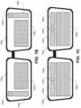
- An example layout of one binocular waveguide display is illustrated in FIG. 1B .
- the display includes waveguides 152a, 152b for the left and right eyes, respectively.
- the waveguides include in-couplers 154a,b, pupil expanders 156a,b, and components 158a,b, which operate as both out-couplers and horizontal pupil expanders.
- the pupil expanders 156a,b are arranged along an optical path between the in-coupler and the out-coupler.
- An image generator (not shown) may be provided for each eye and arranged to project light representing an image on the respective in-coupler.
- FIG.1C An example layout of another binocular waveguide display is illustrated in FIG.1C .
- the display includes waveguides 160a, 160b for the left and right eyes, respectively.
- the waveguides include in-couplers 162a,b. Light from different portions of an image may be coupled by the in-couplers 162a,b to different directions within the waveguides. In-coupled light traveling toward the left passes through pupil expanders 164a,b, while in-coupled light traveling toward the right passes through pupil expanders 166a,b. Having passed through the pupil expanders, light is coupled out of the waveguides using components 168a,b, which operate as both out-couplers and vertical pupil expanders to substantially replicate an image provided at the in-couplers 162a,b.
- different features of the waveguide displays may be provided on different surfaces of the waveguides.
- the in-coupler and the out-coupler may both be arranged on the anterior surface of the waveguide (away from the user's eye).
- the in-coupler and/or the out-coupler may be on a posterior surface of the waveguide (toward the user's eye).
- the in-coupler and out-coupler may be on opposite surfaces of the waveguide.
- one or more of an in-coupler, an out-coupler, and a pupil expander may be present on both surfaces of the waveguide.
- the image generator may be arranged toward the anterior surface or toward the posterior surface of the waveguide.
- the in-coupler is not necessarily on the same side of the waveguide as the image generator. Any pupil expanders in a waveguide may be arranged on the anterior surface, on the posterior surface, or on both surfaces of the waveguide. In displays with more than one waveguide layer, different layers may have different configurations of in-coupler, out-coupler, and pupil expander.
- FIG. 1D is a schematic exploded view of a double waveguide display according to some embodiments, including an image generator 170, a first waveguide (WG 1 ) 172, and a second waveguide (WG 2 ) 174.
- FIG. 1E is a schematic side-view of a double waveguide display according to some embodiments, including an image generator 176, a first waveguide (WG 1 ) 178, and a second waveguide (WG 2 ) 180.
- the first waveguide includes a first transmissive diffractive in-coupler (DG1) 180 and a first diffractive out-coupler (DG6) 182.
- the second waveguide has a second transmissive diffractive in-coupler (DG2) 184, a reflective diffractive in-coupler (DG3) 186, a second diffractive out-coupler (DG4) 188, and a third diffractive out-coupler (DG5) 190.
- DG2 transmissive diffractive in-coupler
- DG3 reflective diffractive in-coupler
- DG4 second diffractive out-coupler
- DG5 third diffractive out-coupler
- Different embodiments may use different arrangements of optical components (such as different arrangements of pupil expanders) on the first and second waveguides.
- FIGs. 1A-1E illustrate the use of waveguides in a near-eye display
- the same principles may be used in other display technologies, such as head up displays for automotive or other uses.
- FIG. 1F is a schematic cross-sectional view of a double waveguide optical device illustrating angles of incident and in-coupled light.
- the grating pitch of one or more diffractive gratings as described herein may be selected based on desired ranges of and relationships between the incident and the in-coupled light.
- the double waveguide device of FIG. 1F may use higher order modes (with absolute value of diffraction order higher than 1) and over-wavelength gratings to provide for a high field of view.
- angles in the air are denoted with the letter ⁇ .
- Angles in the waveguide are denoted with the letter ⁇ are located into the waveguides and measure the angle of rays that have been diffracted.
- the superscript C indicates a critical ray, either in air or in the waveguide, and the superscript G indicates a grazing ray.
- FIG. 1F illustrates an optical device comprising a first optical waveguide WG1 and a second optical waveguide WG2.
- WG1 has refractive index n 3 and WG2 has refractive index n 5 . These refractive indices may be the same, or they may be different from one another.
- Such an optical device is configured for guiding an angular range ⁇ ⁇ WG 1 C , ⁇ WG 1 C of an incident light comprising a range of wavelengths.
- n 5 is a refractive index of the second waveguide's material.
- the first waveguide comprises a diffraction grating having an over-wavelength grating's pitch which is configured for second orders of diffraction. This allows coupling of very high angles of incidence for the ultra-high field of view into the first waveguide WG1. Without using second order diffraction, coupling very high angles of incidence would be very difficult since it would call for a very small grating pitch.
- the angular range ⁇ WG 1 G ⁇ WG 1 C is a symetric angular range of the angular range ⁇ ⁇ WG 1 C , ⁇ ⁇ WG 1 G with respect to the incident axis of the light incident on the optical device.
- the angular range between ⁇ ⁇ WG 1 G , ⁇ WG 1 G also referenced as transmitted beam T 0 , transmits through the diffraction grating of the first waveguide WG1 with a high efficiency.
- the left hand side of the image will propagate toward the left into the waveguide WG1 while the right hand side of the image will propagate toward the right.
- the transmitted beam T 0 has an angular extent from ⁇ ⁇ WG 2 C , ⁇ WG 2 C , the grazing rays being in the vicinity of the normal.
- the transmitted beam T 0 will diffract on a second grating which is on top of the second waveguide WG2 and positive angles of incidence will propagate toward the left in the waveguide WG2 while negative angles of incidence will propagate toward the right into WG2.
- the second grating may differ from the first one by having a different pitch size, but the shapes of the first and second gratings may be similar.
- the shapes of the first and second gratings may be configured to emphasizes nano-jet waves.
- the second grating in the waveguide WG2 may have an over-wavelength grating pitch configured for second orders of diffraction.
- the first and second grating are configured through the grating pitch for diffracting the specific respective angular ranges of the light as specified above for a given wavelength of the light as will be shown below.
- n 1 1
- n 1 is a refractive index of the host material.
- ⁇ WG 1 G and ⁇ WG 2 G are chosen to approximately equal 75°.
- the values chosen for ⁇ WG 1 G and ⁇ WG 2 G may be chosen according to the distance the image has to travel into the waveguide before being extracted, the number of total internal reflection bounces, and the thickness of the waveguide. It is also to be noted that, in the specific example given above, refractive indexes of respectively the first waveguide and the second waveguide are the same, n 2 . However, the first and second waveguides may have different refractive indexes in other embodiments.
- ⁇ WG 2 G is chosen to be -3° for instance. Other values are also possible depending on the design conditions, such as whether it is desired to superimpose the left and right images in the middle of the final image, or if no crossing of the left and right images is desired. In the disclosed embodiment, the value of -3° may lead to a final image that includes the left and right images with a black band in the middle. However, in some applications, the presence of such a band is not desired, and other values for ⁇ WG 2 G can be selected.
- Example embodiments include an over-wavelength in-coupling grating which can generate intensive high diffraction orders for both transverse-electric (TE) polarization and transverse-magnetic (TM) polarization simultaneously.
- TE transverse-electric
- TM transverse-magnetic
- using the double material u-shaped system provides a diffraction grating with high response for both polarizations.
- the size of the elements inside the unit cell of a diffraction grating configured for TM polarization is bigger than the size in a case of the grating configured for TE polarization.
- An example topology may be represented as a u-shaped structure with the high refractive index inserts providing the high efficiency response of the system.
- the sides of a u-shaped structure may be described as ridge regions, and the base of the u-shaped structure may be described as a saddle region, and the inserts may be described as core elements.
- n 1 is the refractive index of the host medium (e.g. the ambient air)
- n 3 is the refractive index of the substrate
- n 1 ⁇ n 3 ⁇ n 2 ⁇ n 4 is the refractive index of the substrate.
- FIG. 2A depicts a cross-sectional view of an example unit cell geometry for a u-shaped diffraction grating with inserts in accordance with some embodiments.
- a schematic perspective cutaway view of a plurality of u-shaped diffraction grating elements with inserts arranged in a diffraction grating structure is provided in FIG. 2B .
- the grating elements are substantially straight and are arranged substantially parallel to one another.
- FIG. 2B some embodiments include thousands of grating elements.
- a grating structure such as that of FIG. 2B may be employed as a diffractive in-coupler or out-coupler for a waveguide display.
- FIG. 2B illustrates a diffractive element 200 that includes a substrate 202.
- a plurality of grating elements 204, 206, 208 are arranged on the substrate.
- Each grating element includes a first ridge region 210 having a first ridge body region 212 and a first core element 214.
- Each grating element further includes a second ridge region 220 having a second ridge body region 222 and a second core element 224.
- a saddle region 226 extends between the first and second ridge regions.
- the first ridge body, the second ridge body, and the saddle region have a first refractive index (n 2 )
- the first core element and second core element have a second refractive index (n 4 ) greater than the first refractive index.
- the saddle regions have a first height (H 1 ) lower than a second height (H 3 ) of the first and second ridge regions.
- the substrate is in contact with a host medium, as illustrated for example at region 270 of the substrate 202.
- the grating elements may be arranged in a one-dimensional grating array.
- the diffractive element 200 of FIG. 2B may alternatively be described as including substrate 202 and a plurality of grating core elements 214, 224, 234, 244, 254, 264 arranged substantially parallel to one another on the substrate, with the grating core elements having the second refractive index (n 4 ).
- a plurality of overlay elements 215, 235, 255 are arranged substantially periodically, each overlay element contiguously covering two adjacent grating core elements.
- the overlay elements have a first refractive index (n 2 ) lower than the second refractive index (n 4 ).
- a diffraction grating is provided, where the diffraction grating has u-shaped unit cells that include insert regions.
- one or more such diffraction gratings are provided for one or more waveguides in a waveguide display with a wide field of view.
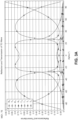
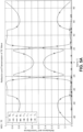
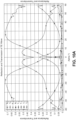
- FIG. 3B depicts the performance of the first grating of the example 2-waveguide system working with TM polarized light of the blue color.
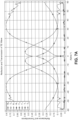
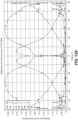
- FIGs. 4A and 4B depict the performance of a second diffraction grating of the example two-waveguide system.
- FIGs. 3A and 3B depict diffraction performances of the first grating.
- the ⁇ 2 diffraction orders have high efficiency and high uniformity for the angular range 30° to 72° (-30° to -72°) and it has a very high transmission efficiency for ⁇ 30° field of view.
- WG1 first waveguide
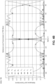
- FIGs. 4A-4B illustrate that the second grating for the second waveguide (WG2) provides high diffraction efficiency.
- FIG. 4A shows about 50% diffraction efficiency for TE polarization of ⁇ 2nd diffraction orders in the angular range -30° to 30°.
- FIG. 4B shows about 80% for TM polarization of ⁇ 2nd diffraction orders in the angular range -30° to 30°.
- FIGs. 4A and 4B illustrate that for the transmitted field of view of ⁇ 30° through the first grating, we get again very high diffraction efficiencies and uniformities over this angular range.
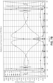
- Some embodiments combine the waveguides for a full RGB system. As it was demonstrated before, analyzing the diffraction performances of the diffraction grating configured for three wavelengths corresponding to red (625nm), green (530nm) and blue (460nm) colors, we can conclude that to get full RGB display system it is enough in some embodiments to use just four waveguides instead of six.
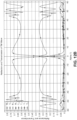
- the transmittivity of 0 diffraction order is of interest for the waves corresponding to green and red colors.
- the presented system has very low transmittivity of 0 diffraction order in the angular range 30° to 20° (-30° to -20°), as seen in FIGs. 5A and 5B .
- FIG. 5A shows reflection and transmission of the TE wave
- FIG. 5B shows reflection and transmission of the TM wave.
- simulations did not take into account the dispersion of material of the inserts at visible wavelengths. This fact can modify, and in some cases improve, the performance of the system.
- Some embodiments include over-wavelength in-coupling gratings with high refractive index single-material u-shaped elements without inserts that can generate strong ⁇ 2nd diffraction orders for both polarizations (TE and TM) simultaneously.
- a cross-sectional view of a single-material u-shaped element is illustrated in FIG. 2C .
- a schematic perspective partial cutaway view of a plurality of single-material u-shaped elements arranged in a diffraction grating structure is provided in FIG. 2D .
- the grating elements are substantially straight and are arranged substantially parallel to one another.
- the grating elements may be curved (e.g.
- grating elements may be concentric with one another). Although only three grating elements are illustrated in FIG. 2D , some embodiments include thousands of grating elements.
- a grating structure such as that of FIG. 2D may be employed as a diffractive in-coupler or out-coupler for a waveguide display.
- FIG. 2D illustrates a diffractive optical element 300 that includes a substrate 302.
- a plurality of grating elements 304, 306, 308 are arranged on the substrate.
- Each of the grating elements includes a first ridge region 310, a second ridge region 312, and a saddle region 314 extending between the first and second ridge regions.
- the saddle region has a first height (H 1 ) lower than a second height (H 3 ) of the first and second ridge regions.
- the saddle region may be contiguous with the ridge regions.
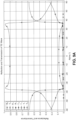
- FIG. 6 is a graph showing values of the refractive index of TiO 2 over a range of wavelengths.
- n 1 1.
- the first grating for the first waveguide (WG1) is configured for the blue color to get high diffraction efficiency of ⁇ 2nd diffraction orders in the angular range 0° to 44° (-44° to 0°).
- this diffraction grating in the angular range of 14.6° to 72° (-14.6° to -72°) will provide high diffraction efficiency of ⁇ 2nd diffraction orders for both polarizations (up to 77% for TE polarization and up to 36% for TM polarization).
- the red color light gets through the first diffraction grating with high transmittivity of 0 order in the angular range -37° to 37°.
- the corresponding input of ⁇ 2nd diffraction orders will be week (less than 15%).
- the grating for WG2 is configured for the green color to get high diffraction efficiency of ⁇ 2nd diffraction orders in the angular range 0° to 44° (-44° to 0°).
- the combination of the responses for both polarizations will provide high diffraction uniformity of total response.
- this diffraction grating will have intensive ⁇ 2nd diffraction orders in the angular range 17° to 86.5° (-86.5° to -17°).
- the transmittivity of 0-order at -17° to 17° is good. It is quite uniform and about 80% for both polarizations.
- TM polarization quite high transmittivity of 0 order at the angles above 17° and below -17° will make an input into the ⁇ 2nd diffraction orders generated by the next waveguide.
- Examples of over-wavelength in-coupling gratings with inserts can generate intensive high diffraction orders for both polarizations (TE and TM) simultaneously.
- two waveguides with diffraction gratings configured for a particular wavelength may be implemented in a monochromatic display system with a substantially hemispherical field of view.
- the combination of the waveguides with u-shaped grating elements with the inserts may be implemented in a full RGB system. To get the full RGB system, some embodiments may use four waveguides instead of six.
- the system may be configured to get the proper balance of the system performance by taking into account the pure response of the system at some angles of incidence.
- silicon may be used as the material of the inserts.
- an over-wavelength in-coupling with a high refractive index dispersive material grating can generate intensive high diffraction orders for both polarizations (TE and TM) simultaneously.
- TE and TM polarizations
- Combining three waveguides with diffraction gratings configured for three wavelengths corresponding to red, green, and blue colors we can get full RGB system with high performance.
- a full RGB stereoscopic system with wide FoV is implemented using four waveguides instead of six. It is also possible to use three waveguides in a case of higher refractive index for the waveguide material.
- an additional waveguide may be used to increase the field of view of the system.
- couplers configured for visible light
- other embodiments are configured for use with longer or shorter wavelengths, such as infrared or ultraviolet light, or for use with waves in other parts of the electromagnetic spectrum.
- Such embodiments may employ materials that are transparent to the wavelengths for which they are designed.
- a diffraction grating structure as described herein may be used as an in-coupler, an out-coupler, or both.
- a waveguide may be provided in which a diffraction grating as described herein is used as an in-coupler and another diffraction grating as described herein is used as an out-coupler.
- the in-coupler and out-coupler may have the same pitch and/or may have other optical properties in common.
- Embodiments using a u-shaped structure to configure the gratings for the high order of diffraction permit the use of a substantially bigger pitch size, allowing for an ease of manufacture that is difficult to achieve in fabrication with the previous art technology.
- the diffractive element is used as an in-coupler of the first waveguide in a two-waveguide system, such as the system illustrated in FIG. 1F .
- the grating elements may be arranged substantially periodically with a pitch between M 1 n 3 + n 5 ⁇ 1 ⁇ and M 1 0.8 n 3 + 0.8 n 5 ⁇ 1 ⁇ where M 1 is an integer representing a diffractive order, ⁇ is a wavelength of incident light, and n 3 is a refractive index of the substrate for the first waveguide.
- the diffractive element is used as an in-coupler of the second waveguide in a two-waveguide system, such as the system illustrated in FIG. 1F .
- the grating elements may be arranged substantially periodically with a pitch between M 2 n 5 ⁇ and M 2 0.8 n 5 ⁇ where M 2 is an integer representing a diffractive order, ⁇ is a wavelength of incident light, and n 5 is a refractive index of the substrate for the second waveguide.
- the grating elements of the diffraction grating are arranged substantially periodically with a pitch between 160nm and 780nm with n 3 and n 5 between 1.5 and 2.0, M 1 and M 2 being either 1 or 2, and a wavelength ( ⁇ ) of incident light between 460nm and 625nm.
- the grating elements are arranged substantially periodically with a pitch between 230nm and 1040nm for n 3 between 1.5 and 2.0, M equal to 1 or 2, where M is the diffraction order for the diffraction gratings, and a wavelength ( ⁇ ) of incident light between 460nm and 625nm.
- a diffractive element includes a substrate and a plurality of grating elements on the substrate, each grating element comprising: a first ridge region comprising a first ridge body region and a first core element; a second ridge region comprising a second ridge body region and a second core element; and a saddle region extending between the first and second ridge regions; wherein the first ridge body, the second ridge body, and the saddle region have a first refractive index (n 2 ), and the first core element and second core element have a second refractive index (n 4 ) greater than the first refractive index.
- the substrate has a third refractive index (n 3 ) that is less than the first refractive index (n 2 ).
- the grating elements are arranged substantially periodically on the substrate.
- the grating elements are arranged substantially periodically with a selected pitch, wherein the pitch is selected based on a wavelength, a third refractive index (n 3 ) of the substrate, and a diffraction order.
- the grating elements are arranged substantially periodically with a pitch between M 2 n 5 ⁇ and M 2 0.8 n 5 ⁇ , where M 2 is an integer (e.g. 1 or 2) representing a diffractive order, ⁇ is a wavelength of incident light, and n 5 is a refractive index of the substrate for the second waveguide.
- the grating elements are arranged substantially periodically with a pitch between M 1 n 3 + n 5 ⁇ 1 ⁇ and M 1 0.8 n 3 + 0.8 n 5 ⁇ 1 ⁇
- M 1 is an integer (e.g. 1 or 2) representing a diffractive order
- ⁇ is a wavelength of incident light
- n 3 is a refractive index of the substrate for the first waveguide.
- the grating elements are arranged substantially periodically with a pitch between 400nm and 800nm.
- the grating elements are arranged substantially periodically with a pitch below 400nm.
- the grating elements are arranged substantially periodically with a pitch above 800nm.
- the first and second ridge regions each have widths between 100nm and 200nm.
- the first and second ridge regions each have a width of between 0.1 and 0.3 of a pitch of the grating elements.
- the saddle region has a first height (H 1 ) and a first width (W 4 ) and the ridge regions each have a second height (H 3 ) and a second width (W 3 ), and wherein H 1 is lower than H 3 ; and H 3 ⁇ H 1 ⁇ W 3 tan ⁇ ′ B with ⁇ ′ B ⁇ ⁇ B ⁇ ⁇ i 2 with ⁇ i being an angle of incident light with respect to a normal to a top surface of on said diffraction grating and ⁇ B ⁇ 90 ° ⁇ sin ⁇ 1 n 1 n 2 2 , n 1 being a refractive index of host medium in which the diffractive element is placed.
- the first width (W 4 ) of the saddle region is less than one third of a pitch of the diffractive element.
- the sum of the first width (W 4 ) and twice the second width (W 3 ) is less than a pitch of the diffractive element.
- the first and second core elements each have widths between 50nm and 200nm.
- the first and second core elements each have widths that are between 0.4 and 0.8 as great as the widths of the first and second ridge regions, respectively.
- the first and second core elements are in contact with the substrate.
- the substrate is in contact with a host medium.
- the plurality of grating elements are substantially straight and are substantially parallel to one another.
- the plurality of grating elements are arranged in a one-dimensional grating.
- the diffractive element is configured as an input coupler of a waveguide.
- the substrate is made of a material selected from the group consisting of glass, plastic, and a polymer material.
- the substrate has a third refractive index (n 3 ) of 1.5 ⁇ 5%.
- the substrate has a third refractive index (n 3 ) that is no greater than about 1.7.
- the substrate has a third refractive index (n 3 ) that is no greater than about 2.0.
- the first ridge region, the second ridge region, and the saddle region consist essentially of TiO 2 .
- the first ridge region, the second ridge region, and the saddle region have a first refractive index (n 2 ) of about 2.5.
- the first ridge region, the second ridge region, and the saddle region have a first refractive index (n 2 ) of greater than 2.0.
- the core refractive index (n 4 ) is greater than 2.5.
- the core refractive index (n 4 ) is greater than 2.0.
- the first and second core elements consist essentially of silicon.
- a method of manufacturing a diffractive element includes: forming, on a substrate, a plurality of grating elements, the forming of each grating element comprising: forming a first core region and a second core region on the substrate; and forming a first ridge body over the first core region, a second ridge body over the second core region, and a saddle region over the substrate between the first core region and the second core region; wherein the first ridge body, the second ridge body, and the saddle region are formed of a material having a first refractive index (n 2 ), and the first core and second core are formed of a material having a core refractive index (n 4 ) greater than the first refractive index.
- a diffractive element comprises: a substrate; a plurality of grating core elements arranged substantially parallel to one another on the substrate, the grating core elements having a core refractive index (n 4 ); and a plurality of overlay elements arranged substantially periodically, each overlay element contiguously covering two adjacent grating core elements, the overlay elements having a first refractive index (n 2 ) lower than the second refractive index (n 4 ).
- each of the grating core elements is substantially covered by one of the overlay elements.
- the core elements are arranged substantially periodically.
- the overlay elements are arranged substantially periodically with a first pitch and the core elements are arranged substantially periodically with a second pitch that is substantially half of the first pitch.
- the overlay elements are substantially parallel to one another and to the grating core elements.
- a method of manufacturing a diffractive element comprises: forming, on a substrate, a plurality of grating core elements arranged substantially parallel to one another on the substrate, the grating core elements having a core refractive index (n 4 ); and forming a plurality of overlay elements, each of the overlay elements contiguously covering two adjacent grating core elements, the overlay elements having a first refractive index (n 2 ) lower than the second refractive index (n 4 ).
- a diffractive element comprises: a substrate; a plurality of grating elements on the substrate, each grating element comprising: a first ridge region; a second ridge region; and a saddle region extending between the first and second ridge regions.
- the grating elements are arranged substantially periodically on the substrate.
- the plurality of grating elements are substantially straight and are substantially parallel to one another.
- the first ridge region, the second ridge region, and the saddle region have a refractive index greater than 2.0 for visible light.
- the first ridge region, the second ridge region, and the saddle region have a refractive index greater than 2.4 for visible light.
- the first ridge region, the second ridge region, and the saddle region have a refractive index of more than 1.2 times as great as a refractive index of the substrate for visible light.
- the first ridge region, the second ridge region, and the saddle region have a refractive index of more than 1.4 times as great as a refractive index of the substrate for visible light.
- the first ridge region, the second ridge region, and the saddle region comprise TiO 2 .
- the first ridge region, the second ridge region, and the saddle region consist essentially of TiO 2 .
- the first ridge region, the second ridge region, and the saddle region are made of a dispersive material.
- a method of manufacturing a diffractive element includes: forming, on a substrate, a plurality of grating elements, the forming of each grating element comprising: forming a first ridge on the substrate, a second ridge on the substrate, and a saddle region on the substrate between the ridge and the second ridge.
- a method includes: directing light having a first wavelength onto a diffractive element, wherein the diffractive element comprises: a substrate having a third refractive index (n 3 ); a plurality of grating elements on the substrate, each grating element comprising: a first ridge region comprising a first ridge body region and a first core element; a second ridge region comprising a second ridge body region and a second core element; and a saddle region extending between the first and second ridge regions; wherein the first ridge body, the second ridge body, and the saddle region have a first refractive index (n 2 ), and the first core element and second core element have a second refractive index (n 4 ) greater than the first refractive index.
- the diffractive element comprises: a substrate having a third refractive index (n 3 ); a plurality of grating elements on the substrate, each grating element comprising: a first ridge region comprising a first ridge body region and a first core
- the grating elements are arranged substantially periodically with a pitch of between 1.0 and 1.2 times as great as the first wavelength.
- the grating elements are arranged substantially periodically with a pitch between 400nm and 800nm, wherein the third refractive index (n 3 ) is 1.52, and wherein the first wavelength is between 450nm and 700nm.
- the grating elements are arranged substantially periodically with a pitch between 400nm and 800nm, wherein the third refractive index (n 3 ) is 1.5 ⁇ 5%, wherein the first wavelength is between 450nm and 700nm, and wherein the diffractive element diffracts at least a portion of the light into a second diffractive order.
- the light is unpolarized light.
- the light comprises TE-polarized light and TM-polarized light.
- the first ridge region, the second ridge region, and the saddle region have a refractive index of greater than 2.0 and the substrate has a refractive index of less than 2.0.
Landscapes
- Physics & Mathematics (AREA)
- General Physics & Mathematics (AREA)
- Optics & Photonics (AREA)
- Diffracting Gratings Or Hologram Optical Elements (AREA)
Claims (13)
- Beugungselement (200), umfassend:ein Substrat (202);mehrere Gitterelemente (204) auf dem Substrat (202), wobei jedes Gitterelement einen u-förmigen Querschnitt aufweist, umfassend:eine erste Erhöhungsregion (210);eine zweite Erhöhungsregion (220); undeine Sattelregion (226), die sich zwischen der ersten und der zweiten Erhöhungsregion erstreckt, wobei die Sattelregion eine erste Höhe, H1, aufweist, die niedriger ist als eine zweite Höhe, H3, der ersten und der zweiten Erhöhungsregion;wobei die erste Erhöhungsregion eine erste Erhöhungskörperregion (212) mit einem ersten Brechungsindex, n2, und ein erstes Kernelement (214) innerhalb der ersten Erhöhungskörperregion umfasst, wobei das erste Kernelement einen zweiten Brechungsindex, n4, aufweist, der größer als der erste Brechungsindex ist; unddie zweite Erhöhungsregion eine zweite Erhöhungskörperregion (222) mit dem ersten Brechungsindex, n2, und ein zweites Kernelement (224) innerhalb der zweiten Erhöhungskörperregion umfasst, wobei das zweite Kernelement den zweiten Brechungsindex, n4, aufweist.
- Beugungselement nach Anspruch 1, wobei das erste und das zweite Kernelement in Kontakt mit dem Substrat stehen.
- Beugungselement nach Anspruch 1, wobei das Substrat einen dritten Brechungsindex, n3, aufweist, der kleiner als erste Brechungsindex, n2, ist.
- Beugungselement nach einem der vorangehenden Ansprüche, wobei die Gitterelemente periodisch auf dem Substrat mit einem Gitterrasterabstand angeordnet sind.
- Beugungselement nach Anspruch 4, wobei die Sattelregion eine erste Breite, W4, aufweist, die Erhöhungsregionen jeweils eine zweite Breite, W3, aufweisen, und die Summe aus der ersten Breite, W4, und dem Zweifachen der zweiten Breite, W3, kleiner als der Gitterrasterabstand ist.
- Beugungselement nach einem der vorangehenden Ansprüche, wobei das erste Kernelement und das zweite Kernelement im Wesentlichen aus Silizium bestehen.
- Beugungselement nach einem der vorangehenden Ansprüche, wobei das Substrat zwischen aufeinanderfolgenden Gitterelementen in dem Beugungselement in Kontakt mit der Umgebungsluft steht.
- Beugungselement nach einem der vorangehenden Ansprüche, wobei das Substrat ein Wellenleiter eines Wellenleiter-Displays ist.
- Verfahren, das umfasst:
Richten von Licht, das eine erste Wellenlänge, λ, aufweist, auf ein Beugungselement (200), wobei das Beugungselement (200) umfasst:ein Substrat (202);mehrere Gitterelemente (204) auf dem Substrat (202), wobei jedes Gitterelement einen u-förmigen Querschnitt aufweist, umfassend:eine erste Erhöhungsregion (210);eine zweite Erhöhungsregion (220); undeine Sattelregion (226), die sich zwischen der ersten und der zweiten Erhöhungsregion erstreckt, wobei die Sattelregion eine erste Höhe, H1, aufweist, die niedriger ist als eine zweite Höhe, H3, der ersten und der zweiten Erhöhungsregion;wobei die erste Erhöhungsregion (210) eine erste Erhöhungskörperregion (212) mit einem ersten Brechungsindex, n2, und ein erstes Kernelement (214) innerhalb der ersten Erhöhungskörperregion umfasst, wobei das erste Kernelement einen zweiten Brechungsindex, n4, aufweist, der größer als der erste Brechungsindex ist; unddie zweite Erhöhungsregion (220) eine zweite Erhöhungskörperregion (222) mit dem ersten Brechungsindex, n2, und ein zweites Kernelement (224) innerhalb der zweiten Erhöhungskörperregion umfasst, wobei das zweite Kernelement den zweiten Brechungsindex, n4, aufweist. - Verfahren nach Anspruch 9, wobei das Substrat einen dritten Brechungsindex, n5, aufweist, wobei das Verfahren des Weiteren das Beugen des Lichts bis zu einer Beugungsordnung M2 umfasst, und wobei die Gitterelemente im Wesentlichen periodisch mit einem Rasterabstand angeordnet sind zwischen


- Verfahren nach Anspruch 10, wobei M2 = 2.
- Verfahren nach einem der Ansprüche 9-11, wobei die Sattelregion eine erste Breite, W4, aufweist, die Erhöhungsregionen jeweils eine zweite Breite, W3, aufweisen, und die Summe aus der ersten Breite, W4, und dem Zweifachen der zweiten Breite, W3, kleiner als der Gitterrasterabstand ist.
- Verfahren nach Anspruch 9, wobei das erste Kernelement und das zweite Kernelement im Wesentlichen aus Silizium bestehen.
Applications Claiming Priority (2)
| Application Number | Priority Date | Filing Date | Title |
|---|---|---|---|
| EP20315043 | 2020-03-23 | ||
| PCT/EP2021/057273 WO2021191150A1 (en) | 2020-03-23 | 2021-03-22 | Unpolarized light grating in-coupler |
Publications (2)
| Publication Number | Publication Date |
|---|---|
| EP4127789A1 EP4127789A1 (de) | 2023-02-08 |
| EP4127789B1 true EP4127789B1 (de) | 2025-04-30 |
Family
ID=70482541
Family Applications (1)
| Application Number | Title | Priority Date | Filing Date |
|---|---|---|---|
| EP21713018.6A Active EP4127789B1 (de) | 2020-03-23 | 2021-03-22 | Unpolarisiertes lichtgitter in einem koppler |
Country Status (4)
| Country | Link |
|---|---|
| US (1) | US20230134576A1 (de) |
| EP (1) | EP4127789B1 (de) |
| CN (1) | CN115398284A (de) |
| WO (1) | WO2021191150A1 (de) |
Families Citing this family (4)
| Publication number | Priority date | Publication date | Assignee | Title |
|---|---|---|---|---|
| EP4127820A1 (de) | 2020-03-23 | 2023-02-08 | InterDigital CE Patent Holdings, SAS | Wellenleiteranzeigesystem mit breitem sichtfeld |
| CN116324587A (zh) | 2020-08-13 | 2023-06-23 | 交互数字Ce专利控股有限公司 | 通过c形平面光学架构的低失真成像 |
| CN114002849B (zh) * | 2022-01-04 | 2022-04-08 | 南昌虚拟现实研究院股份有限公司 | 一种衍射光波导显示装置 |
| FI131822B1 (en) * | 2023-05-03 | 2025-12-17 | Dispelix Oy | Display construction |
Family Cites Families (16)
| Publication number | Priority date | Publication date | Assignee | Title |
|---|---|---|---|---|
| US7139128B2 (en) * | 2003-01-06 | 2006-11-21 | Polychromix Corporation | Diffraction grating having high throughput efficiency |
| EP1932050A2 (de) * | 2005-09-14 | 2008-06-18 | Mirage Innovations Ltd. | Beugende optische einrichtung und system |
| JP4721924B2 (ja) * | 2005-12-09 | 2011-07-13 | 富士通株式会社 | 光導波路を伝搬する光と回折格子とを結合させた光素子 |
| CA2662733A1 (en) * | 2006-09-12 | 2008-03-20 | Onechip Photonics Inc. | Coupling-enhanced surface etched gratings |
| JP4312239B2 (ja) * | 2007-02-16 | 2009-08-12 | 富士通株式会社 | 光素子及びその製造方法 |
| WO2009083977A2 (en) * | 2008-01-02 | 2009-07-09 | Mirage Innovations Ltd. | Optical device for relaying polychromatic light |
| US9651729B2 (en) * | 2010-04-16 | 2017-05-16 | Flex Lighting Ii, Llc | Reflective display comprising a frontlight with extraction features and a light redirecting optical element |
| JP2013047763A (ja) * | 2011-08-29 | 2013-03-07 | Tohoku Univ | 周期構造反射鏡およびそれを用いた光素子 |
| KR20140137351A (ko) * | 2012-02-27 | 2014-12-02 | 스미토모 베이클리트 컴퍼니 리미티드 | 광도파로, 광배선 부품, 광도파로 모듈 및 전자 기기 |
| US9513480B2 (en) | 2015-02-09 | 2016-12-06 | Microsoft Technology Licensing, Llc | Waveguide |
| US9791703B1 (en) | 2016-04-13 | 2017-10-17 | Microsoft Technology Licensing, Llc | Waveguides with extended field of view |
| KR20240074923A (ko) * | 2017-01-27 | 2024-05-28 | 매직 립, 인코포레이티드 | 상이하게 배향된 나노빔들을 갖는 메타표면들에 의해 형성된 회절 격자 |
| US10534115B1 (en) * | 2017-09-22 | 2020-01-14 | Facebook Technologies, Llc | Gray-tone electron-beam lithography |
| WO2019079679A1 (en) * | 2017-10-20 | 2019-04-25 | Magic Leap, Inc. | CONFIGURING OPTICAL LAYERS IN PRINTING LITHOGRAPHY METHODS |
| EP3540479A1 (de) * | 2018-03-13 | 2019-09-18 | Thomson Licensing | Beugungsgitter mit doppelmaterialstrukturen |
| EP3588150A1 (de) | 2018-06-29 | 2020-01-01 | Thomson Licensing | Optische vorrichtung mit mehrschichtigen wellenleitern |
-
2021
- 2021-03-22 EP EP21713018.6A patent/EP4127789B1/de active Active
- 2021-03-22 CN CN202180028516.5A patent/CN115398284A/zh active Pending
- 2021-03-22 WO PCT/EP2021/057273 patent/WO2021191150A1/en not_active Ceased
- 2021-03-22 US US17/911,331 patent/US20230134576A1/en active Pending
Also Published As
| Publication number | Publication date |
|---|---|
| WO2021191150A1 (en) | 2021-09-30 |
| CN115398284A (zh) | 2022-11-25 |
| EP4127789A1 (de) | 2023-02-08 |
| US20230134576A1 (en) | 2023-05-04 |
Similar Documents
| Publication | Publication Date | Title |
|---|---|---|
| EP4031927B1 (de) | Optische vorrichtung zum koppeln eines hohen blickfeldes von einfallendem licht | |
| EP4127789B1 (de) | Unpolarisiertes lichtgitter in einem koppler | |
| CN113544551B (zh) | 光学设备 | |
| CN109073882B (zh) | 具有出射光瞳扩展器的基于波导的显示器 | |
| CA2956872C (en) | Exit pupil expanding diffractive optical waveguiding device | |
| EP4133325B1 (de) | Wellenleiteranzeige mit kreuzpolarisierten augenpupillenexpandierern | |
| US12326562B2 (en) | Waveguide display system with wide field of view | |
| US20230400618A1 (en) | Single mode full color waveguide combiner using asymmetric transmissive and reflective diffraction gratings | |
| US20240361592A1 (en) | Full color eye-pupil-expanders with high vertical field of view | |
| US12449583B2 (en) | Low distortion imaging through a C-shape flat optical architecture | |
| EP4352553A1 (de) | Doppelbeugungsgitter-inkoppler für reduzierte wellenleiterdicke | |
| WO2022008378A1 (en) | Reflective in-coupler design with high refractive index element using second diffraction order for near-eye displays | |
| US20240094537A1 (en) | Uniform incoupler for conical incidence | |
| EP4176302B1 (de) | Vollfarbiger wellenleiterkombinierer mit eingebetteter metagitterung | |
| WO2021233877A1 (en) | High-uniformity high refractive index material transmissive and reflective diffraction gratings | |
| EP4154043B1 (de) | Doppelmaterialbeugungsgitter mit hoher farbuniformität und stufenförmigen hohlräumen |
Legal Events
| Date | Code | Title | Description |
|---|---|---|---|
| STAA | Information on the status of an ep patent application or granted ep patent |
Free format text: STATUS: UNKNOWN |
|
| STAA | Information on the status of an ep patent application or granted ep patent |
Free format text: STATUS: THE INTERNATIONAL PUBLICATION HAS BEEN MADE |
|
| PUAI | Public reference made under article 153(3) epc to a published international application that has entered the european phase |
Free format text: ORIGINAL CODE: 0009012 |
|
| STAA | Information on the status of an ep patent application or granted ep patent |
Free format text: STATUS: REQUEST FOR EXAMINATION WAS MADE |
|
| 17P | Request for examination filed |
Effective date: 20220919 |
|
| AK | Designated contracting states |
Kind code of ref document: A1 Designated state(s): AL AT BE BG CH CY CZ DE DK EE ES FI FR GB GR HR HU IE IS IT LI LT LU LV MC MK MT NL NO PL PT RO RS SE SI SK SM TR |
|
| DAV | Request for validation of the european patent (deleted) | ||
| DAX | Request for extension of the european patent (deleted) | ||
| GRAP | Despatch of communication of intention to grant a patent |
Free format text: ORIGINAL CODE: EPIDOSNIGR1 |
|
| STAA | Information on the status of an ep patent application or granted ep patent |
Free format text: STATUS: GRANT OF PATENT IS INTENDED |
|
| INTG | Intention to grant announced |
Effective date: 20241118 |
|
| GRAS | Grant fee paid |
Free format text: ORIGINAL CODE: EPIDOSNIGR3 |
|
| GRAA | (expected) grant |
Free format text: ORIGINAL CODE: 0009210 |
|
| STAA | Information on the status of an ep patent application or granted ep patent |
Free format text: STATUS: THE PATENT HAS BEEN GRANTED |
|
| P01 | Opt-out of the competence of the unified patent court (upc) registered |
Free format text: CASE NUMBER: APP_13080/2025 Effective date: 20250317 |
|
| AK | Designated contracting states |
Kind code of ref document: B1 Designated state(s): AL AT BE BG CH CY CZ DE DK EE ES FI FR GB GR HR HU IE IS IT LI LT LU LV MC MK MT NL NO PL PT RO RS SE SI SK SM TR |
|
| REG | Reference to a national code |
Ref country code: CH Ref legal event code: EP Ref country code: GB Ref legal event code: FG4D |
|
| REG | Reference to a national code |
Ref country code: IE Ref legal event code: FG4D |
|
| REG | Reference to a national code |
Ref country code: DE Ref legal event code: R096 Ref document number: 602021029981 Country of ref document: DE |
|
| REG | Reference to a national code |
Ref country code: NL Ref legal event code: MP Effective date: 20250430 |
|
| REG | Reference to a national code |
Ref country code: AT Ref legal event code: MK05 Ref document number: 1790514 Country of ref document: AT Kind code of ref document: T Effective date: 20250430 |
|
| PG25 | Lapsed in a contracting state [announced via postgrant information from national office to epo] |
Ref country code: FI Free format text: LAPSE BECAUSE OF FAILURE TO SUBMIT A TRANSLATION OF THE DESCRIPTION OR TO PAY THE FEE WITHIN THE PRESCRIBED TIME-LIMIT Effective date: 20250430 Ref country code: ES Free format text: LAPSE BECAUSE OF FAILURE TO SUBMIT A TRANSLATION OF THE DESCRIPTION OR TO PAY THE FEE WITHIN THE PRESCRIBED TIME-LIMIT Effective date: 20250430 Ref country code: PT Free format text: LAPSE BECAUSE OF FAILURE TO SUBMIT A TRANSLATION OF THE DESCRIPTION OR TO PAY THE FEE WITHIN THE PRESCRIBED TIME-LIMIT Effective date: 20250901 |
|
| REG | Reference to a national code |
Ref country code: LT Ref legal event code: MG9D |
|
| PG25 | Lapsed in a contracting state [announced via postgrant information from national office to epo] |
Ref country code: NO Free format text: LAPSE BECAUSE OF FAILURE TO SUBMIT A TRANSLATION OF THE DESCRIPTION OR TO PAY THE FEE WITHIN THE PRESCRIBED TIME-LIMIT Effective date: 20250730 Ref country code: GR Free format text: LAPSE BECAUSE OF FAILURE TO SUBMIT A TRANSLATION OF THE DESCRIPTION OR TO PAY THE FEE WITHIN THE PRESCRIBED TIME-LIMIT Effective date: 20250731 |
|
| PG25 | Lapsed in a contracting state [announced via postgrant information from national office to epo] |
Ref country code: NL Free format text: LAPSE BECAUSE OF FAILURE TO SUBMIT A TRANSLATION OF THE DESCRIPTION OR TO PAY THE FEE WITHIN THE PRESCRIBED TIME-LIMIT Effective date: 20250430 Ref country code: PL Free format text: LAPSE BECAUSE OF FAILURE TO SUBMIT A TRANSLATION OF THE DESCRIPTION OR TO PAY THE FEE WITHIN THE PRESCRIBED TIME-LIMIT Effective date: 20250430 |
|
| PG25 | Lapsed in a contracting state [announced via postgrant information from national office to epo] |
Ref country code: BG Free format text: LAPSE BECAUSE OF FAILURE TO SUBMIT A TRANSLATION OF THE DESCRIPTION OR TO PAY THE FEE WITHIN THE PRESCRIBED TIME-LIMIT Effective date: 20250430 |
|
| PG25 | Lapsed in a contracting state [announced via postgrant information from national office to epo] |
Ref country code: HR Free format text: LAPSE BECAUSE OF FAILURE TO SUBMIT A TRANSLATION OF THE DESCRIPTION OR TO PAY THE FEE WITHIN THE PRESCRIBED TIME-LIMIT Effective date: 20250430 |
|
| PG25 | Lapsed in a contracting state [announced via postgrant information from national office to epo] |
Ref country code: AT Free format text: LAPSE BECAUSE OF FAILURE TO SUBMIT A TRANSLATION OF THE DESCRIPTION OR TO PAY THE FEE WITHIN THE PRESCRIBED TIME-LIMIT Effective date: 20250430 |
|
| PG25 | Lapsed in a contracting state [announced via postgrant information from national office to epo] |
Ref country code: RS Free format text: LAPSE BECAUSE OF FAILURE TO SUBMIT A TRANSLATION OF THE DESCRIPTION OR TO PAY THE FEE WITHIN THE PRESCRIBED TIME-LIMIT Effective date: 20250731 |
|
| PG25 | Lapsed in a contracting state [announced via postgrant information from national office to epo] |
Ref country code: IS Free format text: LAPSE BECAUSE OF FAILURE TO SUBMIT A TRANSLATION OF THE DESCRIPTION OR TO PAY THE FEE WITHIN THE PRESCRIBED TIME-LIMIT Effective date: 20250830 |
|
| PG25 | Lapsed in a contracting state [announced via postgrant information from national office to epo] |
Ref country code: LV Free format text: LAPSE BECAUSE OF FAILURE TO SUBMIT A TRANSLATION OF THE DESCRIPTION OR TO PAY THE FEE WITHIN THE PRESCRIBED TIME-LIMIT Effective date: 20250430 |
|
| PG25 | Lapsed in a contracting state [announced via postgrant information from national office to epo] |
Ref country code: SM Free format text: LAPSE BECAUSE OF FAILURE TO SUBMIT A TRANSLATION OF THE DESCRIPTION OR TO PAY THE FEE WITHIN THE PRESCRIBED TIME-LIMIT Effective date: 20250430 Ref country code: DK Free format text: LAPSE BECAUSE OF FAILURE TO SUBMIT A TRANSLATION OF THE DESCRIPTION OR TO PAY THE FEE WITHIN THE PRESCRIBED TIME-LIMIT Effective date: 20250430 |
|
| PG25 | Lapsed in a contracting state [announced via postgrant information from national office to epo] |
Ref country code: CZ Free format text: LAPSE BECAUSE OF FAILURE TO SUBMIT A TRANSLATION OF THE DESCRIPTION OR TO PAY THE FEE WITHIN THE PRESCRIBED TIME-LIMIT Effective date: 20250430 |
|
| PG25 | Lapsed in a contracting state [announced via postgrant information from national office to epo] |
Ref country code: EE Free format text: LAPSE BECAUSE OF FAILURE TO SUBMIT A TRANSLATION OF THE DESCRIPTION OR TO PAY THE FEE WITHIN THE PRESCRIBED TIME-LIMIT Effective date: 20250430 |
|
| PG25 | Lapsed in a contracting state [announced via postgrant information from national office to epo] |
Ref country code: SK Free format text: LAPSE BECAUSE OF FAILURE TO SUBMIT A TRANSLATION OF THE DESCRIPTION OR TO PAY THE FEE WITHIN THE PRESCRIBED TIME-LIMIT Effective date: 20250430 |
|
| PG25 | Lapsed in a contracting state [announced via postgrant information from national office to epo] |
Ref country code: IT Free format text: LAPSE BECAUSE OF FAILURE TO SUBMIT A TRANSLATION OF THE DESCRIPTION OR TO PAY THE FEE WITHIN THE PRESCRIBED TIME-LIMIT Effective date: 20250430 |
|
| REG | Reference to a national code |
Ref country code: DE Ref legal event code: R097 Ref document number: 602021029981 Country of ref document: DE |
|
| PLBE | No opposition filed within time limit |
Free format text: ORIGINAL CODE: 0009261 |
|
| STAA | Information on the status of an ep patent application or granted ep patent |
Free format text: STATUS: NO OPPOSITION FILED WITHIN TIME LIMIT |
|
| REG | Reference to a national code |
Ref country code: CH Ref legal event code: L10 Free format text: ST27 STATUS EVENT CODE: U-0-0-L10-L00 (AS PROVIDED BY THE NATIONAL OFFICE) Effective date: 20260311 |
|
| 26N | No opposition filed |
Effective date: 20260202 |
|
| PGFP | Annual fee paid to national office [announced via postgrant information from national office to epo] |
Ref country code: GB Payment date: 20260319 Year of fee payment: 6 |
|
| PGFP | Annual fee paid to national office [announced via postgrant information from national office to epo] |
Ref country code: DE Payment date: 20260320 Year of fee payment: 6 |
|
| PGFP | Annual fee paid to national office [announced via postgrant information from national office to epo] |
Ref country code: FR Payment date: 20260323 Year of fee payment: 6 |