EP4031927B1 - Optische vorrichtung zum koppeln eines hohen blickfeldes von einfallendem licht - Google Patents
Optische vorrichtung zum koppeln eines hohen blickfeldes von einfallendem licht Download PDFInfo
- Publication number
- EP4031927B1 EP4031927B1 EP20771595.4A EP20771595A EP4031927B1 EP 4031927 B1 EP4031927 B1 EP 4031927B1 EP 20771595 A EP20771595 A EP 20771595A EP 4031927 B1 EP4031927 B1 EP 4031927B1
- Authority
- EP
- European Patent Office
- Prior art keywords
- waveguide
- coupler
- diffractive
- angular range
- diffraction
- Prior art date
- Legal status (The legal status is an assumption and is not a legal conclusion. Google has not performed a legal analysis and makes no representation as to the accuracy of the status listed.)
- Active
Links
Images


Classifications
-
- G—PHYSICS
- G02—OPTICS
- G02B—OPTICAL ELEMENTS, SYSTEMS OR APPARATUS
- G02B27/00—Optical systems or apparatus not provided for by any of the groups G02B1/00 - G02B26/00, G02B30/00
- G02B27/01—Head-up displays
- G02B27/017—Head mounted
- G02B27/0172—Head mounted characterised by optical features
-
- G—PHYSICS
- G02—OPTICS
- G02B—OPTICAL ELEMENTS, SYSTEMS OR APPARATUS
- G02B27/00—Optical systems or apparatus not provided for by any of the groups G02B1/00 - G02B26/00, G02B30/00
- G02B27/42—Diffraction optics, i.e. systems including a diffractive element being designed for providing a diffractive effect
- G02B27/4233—Diffraction optics, i.e. systems including a diffractive element being designed for providing a diffractive effect having a diffractive element [DOE] contributing to a non-imaging application
-
- G—PHYSICS
- G02—OPTICS
- G02B—OPTICAL ELEMENTS, SYSTEMS OR APPARATUS
- G02B5/00—Optical elements other than lenses
- G02B5/18—Diffraction gratings
- G02B5/1866—Transmission gratings characterised by their structure, e.g. step profile, contours of substrate or grooves, pitch variations, materials
-
- G—PHYSICS
- G02—OPTICS
- G02B—OPTICAL ELEMENTS, SYSTEMS OR APPARATUS
- G02B6/00—Light guides; Structural details of arrangements comprising light guides and other optical elements, e.g. couplings
- G02B6/0001—Light guides; Structural details of arrangements comprising light guides and other optical elements, e.g. couplings specially adapted for lighting devices or systems
- G02B6/0011—Light guides; Structural details of arrangements comprising light guides and other optical elements, e.g. couplings specially adapted for lighting devices or systems the light guides being planar or of plate-like form
- G02B6/0013—Means for improving the coupling-in of light from the light source into the light guide
- G02B6/0015—Means for improving the coupling-in of light from the light source into the light guide provided on the surface of the light guide or in the bulk of it
- G02B6/0016—Grooves, prisms, gratings, scattering particles or rough surfaces
-
- G—PHYSICS
- G02—OPTICS
- G02B—OPTICAL ELEMENTS, SYSTEMS OR APPARATUS
- G02B6/00—Light guides; Structural details of arrangements comprising light guides and other optical elements, e.g. couplings
- G02B6/10—Light guides; Structural details of arrangements comprising light guides and other optical elements, e.g. couplings of the optical waveguide type
- G02B6/12—Light guides; Structural details of arrangements comprising light guides and other optical elements, e.g. couplings of the optical waveguide type of the integrated circuit kind
- G02B6/122—Basic optical elements, e.g. light-guiding paths
- G02B6/124—Geodesic lenses or integrated gratings
-
- G—PHYSICS
- G02—OPTICS
- G02B—OPTICAL ELEMENTS, SYSTEMS OR APPARATUS
- G02B6/00—Light guides; Structural details of arrangements comprising light guides and other optical elements, e.g. couplings
- G02B6/24—Coupling light guides
- G02B6/26—Optical coupling means
- G02B6/34—Optical coupling means utilising prism or grating
-
- G—PHYSICS
- G02—OPTICS
- G02B—OPTICAL ELEMENTS, SYSTEMS OR APPARATUS
- G02B27/00—Optical systems or apparatus not provided for by any of the groups G02B1/00 - G02B26/00, G02B30/00
- G02B27/01—Head-up displays
- G02B27/0101—Head-up displays characterised by optical features
- G02B2027/0112—Head-up displays characterised by optical features comprising device for genereting colour display
-
- G—PHYSICS
- G02—OPTICS
- G02B—OPTICAL ELEMENTS, SYSTEMS OR APPARATUS
- G02B27/00—Optical systems or apparatus not provided for by any of the groups G02B1/00 - G02B26/00, G02B30/00
- G02B27/01—Head-up displays
- G02B27/0101—Head-up displays characterised by optical features
- G02B2027/0123—Head-up displays characterised by optical features comprising devices increasing the field of view
-
- G—PHYSICS
- G02—OPTICS
- G02B—OPTICAL ELEMENTS, SYSTEMS OR APPARATUS
- G02B27/00—Optical systems or apparatus not provided for by any of the groups G02B1/00 - G02B26/00, G02B30/00
- G02B27/01—Head-up displays
- G02B27/017—Head mounted
- G02B2027/0178—Eyeglass type
Definitions
- the present disclosure relates to the field of optics and photonics, and more specifically to optical device for coupling light incident on the optical device. It may find applications in the field of conformable and wearable optics (i.e. AR/VR glasses (Augmented Reality/Virtual Reality)), as well as in a variety of other electronic consumer products comprising displays and/or lightweight imaging systems.
- conformable and wearable optics i.e. AR/VR glasses (Augmented Reality/Virtual Reality)
- AR/VR glasses Algmented Reality/Virtual Reality
- AR/VR glasses are considered as the next generation human-machine interface, thus raising significant interest of major industrial players in the domain of consumer electronics and mobile devices.
- Development of AR/VR glasses is associated with a number of challenges, including reduction of size and weight of such devices as well as improvement of the image quality (in terms of contrast, field of view, color depth, etc.) that should be realistic enough to enable a truly immersive user experience.
- optical components The tradeoff between the image quality and physical size of the optical components motivates research into ultra-compact optical components that can be used as building blocks for more complex optical systems, such as AR/VR glasses. Such optical components shall also be easy to fabricate and replicate.
- various types of refractive and diffractive lenses and beam-forming components are used to guide the light from a micro-display or a projector towards the human eye, allowing forming a virtual image that is superimposed with an image of the physical world seen with a naked eye (in case of AR glasses) or captured by a camera (in case of VR glasses).
- Some kinds of AR/VR glasses utilizes an optical waveguide wherein light propagates into the optical waveguide by TIR (for Total Internal Reflection) only over a limited range of internal angles.
- the FoV (for Field of View) of the waveguide depends on the material of the waveguide.
- the FoV of a waveguide may be represented by the maximum span of ⁇ 1 + ⁇ ⁇ 1 ⁇ which propagates into the waveguide by TIR.
- the biggest angular span that can be coupled into the waveguide is defined by two rays: the critical ray ( in FIG. 2A ) having incident angle and the grazing ray ( in FIG. 2A ) having incident angle .
- the critical ray is the light ray that just diffracts into the waveguide at the critical angle , which may be determined by , where n 2 ( ⁇ ) is the refractive index of the waveguide's material at the wavelength ⁇ of the incident light. Above the critical angle , total internal reflection (TIR) occurs.
- the grazing ray is the ray having an input angle that diffracts into the waveguide at grazing incidence
- the theoretical FoV of a waveguide presented above is for a single mode system where one single diffraction mode is used to carry the image: either +1 or -1 diffraction mode.
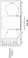
- the field of view in systems based on optical waveguides is limited by the angular bandwidth of the glass plate. If we diffract one mode into the glass plate, the FoV is given as a function of the index of refraction of the material of the glass plate.
- FIG. 3 shows a graph for reasonable ranges of n 2 .
- the field of view of an optical waveguide can be further extended by taking advantage of a second direction of propagation inside of the waveguide, doubling it.
- a waveguide with extended Field of View is proposed wherein a dual mode image propagation is used. In this method, they use the diffraction mode +1 to carry the right hand side image (negative angles of incidence on the in-coupler) in one direction and the -1 mode to propagate the positive angles of incidence into the opposite direction into the waveguide.
- FIG. 2B wherein critical angle and grazing angle are shown for both diffraction modes.
- an optical waveguide comprising a diffraction grating configured to diffract a light of at least one given wavelength incident on the optical waveguide.
- the diffraction grating has a grating pitch above the at least one given wavelength and is configured to diffract the incident light at a diffraction order
- Publication WO 2018/175488 A1 discloses an optical device, comprising: a plurality of waveguides formed over one another and having formed thereon respective diffraction gratings, wherein the respective diffraction gratings are configured to diffract visible light incident thereon into respective waveguides, such that visible light diffracted into the respective waveguides propagates therewithin, wherein the respective diffraction gratings are configured to diffract the visible light incident on the respective waveguides within respective field of views (FOVs) into the respective waveguides with respect to layer normal directions of the respective waveguides, and wherein the respective FOVs are such that the plurality of waveguides are configured to diffract the visible light within a combined FOV that is continuous and greater than each of the respective FOVs.
- FOVs field of views
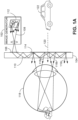
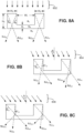
- FIG. 1A is a schematic cross-sectional side view of a waveguide display device in operation.
- An image is projected by an image generator 102.
- the image generator 102 may use one or more of various techniques for projecting an image.
- the image generator 102 may be a laser beam scanning (LBS) projector, a liquid crystal display (LCD), a light-emitting diode (LED) display (including an organic LED (OLED) or micro LED ( ⁇ LED) display), a digital light processor (DLP), a liquid crystal on silicon (LCoS) display, or other type of image generator or light engine.
- LBS laser beam scanning
- LCD liquid crystal display
- LED light-emitting diode
- ⁇ LED micro LED
- DLP digital light processor
- LCDoS liquid crystal on silicon
- Light representing an image 112 generated by the image generator 102 is coupled into a waveguide 104 by a diffractive in-coupler 106.
- the in-coupler 106 diffracts the light representing the image 112 into one or more diffractive orders.
- light ray108 which is one of the light rays representing a portion of the bottom of the image, is diffracted by the in-coupler 106, and one of the diffracted orders 110 (e.g. the second order) is at an angle that is capable of being propagated through the waveguide 104 by total internal reflection.
- At least a portion of the light 110 that has been coupled into the waveguide 104 by the diffractive in-coupler 106 is coupled out of the waveguide by a diffractive out-coupler 114.
- At least some of the light coupled out of the waveguide 104 replicates the incident angle of light coupled into the waveguide.
- out-coupled light rays 116a, 116b, and 116c replicate the angle of the in-coupled light ray 108. Because light exiting the out-coupler replicates the directions of light that entered the in-coupler, the waveguide substantially replicates the original image 112. A user's eye 118 can focus on the replicated image.
- the out-coupler 114 out-couples only a portion of the light with each reflection allowing a single input beam (such as beam 108) to generate multiple parallel output beams (such as beams 116a, 116b, and 116c). In this way, at least some of the light originating from each portion of the image is likely to reach the user's eye even if the eye is not perfectly aligned with the center of the out-coupler. For example, if the eye 118 were to move downward, beam 116c may enter the eye even if beams 116a and 116b do not, so the user can still perceive the bottom of the image 112 despite the shift in position.
- the out-coupler 114 thus operates in part as an exit pupil expander in the vertical direction.
- the waveguide may also include one or more additional exit pupil expanders (not shown in FIG. 1A ) to expand the exit pupil in the horizontal direction.
- the waveguide 104 is at least partly transparent with respect to light originating outside the waveguide display.
- the light 120 from real-world objects such as object 122 traverses the waveguide 104, allowing the user to see the real-world objects while using the waveguide display.
- the diffraction grating 114 As light 120 from real-world objects also goes through the diffraction grating 114, there will be multiple diffraction orders and hence multiple images.
- the diffraction order zero no deviation by 114 to have a great diffraction efficiency for light 120 and order zero, while higher diffraction orders are lower in energy.
- the out-coupler 114 is preferably configured to let through the zero order of the real image. In such embodiments, images displayed by the waveguide display may appear to be superimposed on the real world.
- a waveguide display includes more than one waveguide layer.
- Each waveguide layer may be configured to preferentially convey light with a particular range of wavelengths and/or incident angles from the image generator to the viewer.
- waveguide displays having in-couplers, out-couplers, and pupil expanders may have various different configurations.
- An example layout of one binocular waveguide display is illustrated in FIG. 1B .
- the display includes waveguides 152a, 152b for the left and right eyes, respectively.
- the waveguides include in-couplers 154a,b, pupil expanders 156a,b, and components 158a,b, which operate as both out-couplers and horizontal pupil expanders.
- the pupil expanders 156a,b are arranged along an optical path between the in-coupler and the out-coupler.
- An image generator (not shown) may be provided for each eye and arranged to project light representing an image on the respective in-coupler.
- FIG.1C An example layout of another binocular waveguide display is illustrated in FIG.1C .
- the display includes waveguides 160a, 160b for the left and right eyes, respectively.
- the waveguides include in-couplers 162a,b. Light from different portions of an image may be coupled by the in-couplers 162a,b to different directions within the waveguides. In-coupled light traveling toward the left passes through pupil expanders 164a,b and 165a,b, while in-coupled light traveling toward the right passes through pupil expanders 166a,b and 167a,b. Having passed through the pupil expanders, light is coupled out of the waveguides using out-couplers 168a,b to substantially replicate an image provided at the in-couplers 162a,b.
- different features of the waveguide displays may be provided on different surfaces of the waveguides.
- the in-coupler and the out-coupler may both be arranged on the anterior surface of the waveguide (away from the user's eye).
- the in-coupler and/or the out-coupler may be on a posterior surface of the waveguide (toward the user's eye).
- the in-coupler and out-coupler may be on opposite surfaces of the waveguide.
- one or more of an in-coupler, an out-coupler, and a pupil expander may be present on both surfaces of the waveguide.
- the image generator may be arranged toward the anterior surface or toward the posterior surface of the waveguide.
- the in-coupler is not necessarily on the same side of the waveguide as the image generator. Any pupil expanders in a waveguide may be arranged on the anterior surface, on the posterior surface, or on both surfaces of the waveguide. In displays with more than one waveguide layer, different layers may have different configurations of in-coupler, out-coupler, and pupil expander.
- FIG. 1D is a schematic exploded view of a double waveguide display according to some embodiments, including an image generator 170, a first waveguide (WG 1 ) 172, and a second waveguide (WG 2 ) 174.
- FIG. 1E is a schematic side-view of a double waveguide display according to some embodiments, including an image generator 176, a first waveguide (WG 1 ) 178, and a second waveguide (WG 2 ) 180.
- the first waveguide includes a first transmissive diffractive in-coupler (DG1) 180 and a first diffractive out-coupler (DG6) 182.
- the second waveguide has a second transmissive diffractive in-coupler (DG2) 184, a reflective diffractive in-coupler (DG3) 186, a second diffractive out-coupler (DG4) 188, and a third diffractive out-coupler (DG5) 190.
- DG2 transmissive diffractive in-coupler
- DG3 reflective diffractive in-coupler
- DG4 second diffractive out-coupler
- DG5 third diffractive out-coupler
- Different embodiments may use different arrangements of optical components (such as different arrangements of pupil expanders) on the first and second waveguides.
- FIGs. 1A-1E illustrate the use of waveguides in a near-eye display
- the same principles may be used in other display technologies, such as head up displays for automotive or other uses.
- an optical device providing ultra-high field of view.
- Such an optical device is based on higher order diffraction modes and over-wavelength gratings.
- the optical device comprises waveguides comprising specific diffraction gratings that can be used for in coupling light into the optical device and/or out coupling light from the optical device.
- the diffraction gratings are configured to diffract an incident light at a diffraction order having an absolute value equal to or greater than two.
- such an optical device can be used for AR/VR glasses.
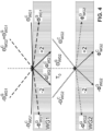
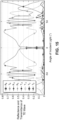
- FIG. 4 An exemplary system is disclosed in FIG. 4 according to an embodiment of the present disclosure.
- FIG. 4 is a schematic cross-sectional view of an in-coupling region of a double waveguide optical device that uses higher order modes (with absolute value of diffraction order higher than one) and over-wavelength gratings for a high Field of View.
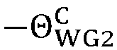
- angles whose name begin with letter ⁇ are located in the air. Angles whose name begins with ⁇ are located in the waveguides and measure the angle of rays that have been diffracted. As previously discussed, C is a critical ray, either in air or in the waveguide, and G is a grazing ray.
- FIG. 4 illustrates an in-coupler portion of an optical device comprising a first optical waveguide WG1 and a second optical waveguide WG2.
- Such an optical device is configured for guiding an angular range [ ⁇ ⁇ WG 1 C , ⁇ WG 1 C ] of an incident light comprising a range of wavelengths.
- n 3 as the refractive index of the second waveguide's material.
- the first waveguide WG1 is placed in front of the second optical waveguide WG2 according to light propagation direction.
- incident light is first transmitted or diffracted by the first waveguide WG1, and then the part of the incident light transmitted by the first waveguide WG1 is transmitted or diffracted by the second waveguide WG2.
- light that exits a diffraction grating with diffractive order zero is referred to as being "transmitted,” while light that exits the diffraction grating with non-zero diffractive order is referred to as having been diffracted.
- the first waveguide comprises a diffraction grating having an over-wavelength grating's pitch which is configured for second orders of diffraction. This allows coupling of very high angles of incidence into the first waveguide WG1.
- Example embodiments that use second order diffraction allow for coupling of very high angles of incidence with the use of a larger grating pitch than would be needed if first order diffraction is used.
- the angular range [ ⁇ WG 1 G , ⁇ WG 1 C ] is a symmetric angular range of the angular range [ ⁇ ⁇ WG 1 C , ⁇ ⁇ WG 1 G ] with respect to the incident axis of the light incident on the optical device.
- the left hand side of the image will propagate in the negative direction (toward the left) into the waveguide WG1 while the right hand side of the image, represented by positive angles of incident light will propagate in the positive direction (toward the right).
- light coupled into the negative direction travels to a first set of one or more eye pupil expanders (such as eye pupil expanders 164a, 165a of FIG. 1C ) before being coupled out of the waveguide by an out-coupler (such as out-coupler 168a of FIG. 1C ), while light coupled into the positive direction travels to a second set of one or more eye pupil expanders (such as eye pupil expanders 166a, 167a of FIG. 1C ) before being coupled out of the waveguide by the out-coupler.
- eye pupil expanders such as eye pupil expanders 164a, 165a of FIG. 1C
- an out-coupler such as out-coupler 168a of FIG. 1C
- light coupled into the positive direction travels to a second set of one or more eye
- the transmitted beam T 0 has an angular extent from [ ⁇ ⁇ WG 2 C , ⁇ WG 2 C ], the grazing rays being in the vicinity of the normal.
- the transmitted beam T 0 will diffract on a second grating which is on the second waveguide WG2, and positive angles of incidence will propagate toward the right in the waveguide WG2 while negative angles of incidence will propagate toward the left into WG2.
- the second grating is different from the first one in that it has a different pitch size.
- the in-coupler diffraction gratings of both waveguides WG1 and WG2 may have a geometrical structure that emphasizes nano jet-waves.
- the in-coupler gratings may have generally the same cross-sectional shape.
- the second grating comprised in the waveguide WG2 has an over-wavelength grating's pitch configured for second orders of diffraction.
- the first and second grating are configured through the grating pitch for diffracting the specific respective angular ranges of the light as specified above for a given wavelength of the light as will be shown below.
- n 1 1.
- M and N correspond respectively to the diffraction order of the first and second diffraction gratings.
- ⁇ WG 1 G and ⁇ WG 2 G may be chosen according to the distance the image has to travel into the waveguide before being extracted, the number of TIR bounces, and the thickness of the waveguide.
- ⁇ WG 2 G is chosen to be -3° for instance. Other values are also possible depending on the design conditions, such as whether it is desired to superimpose the left and right images in the middle of the final image, or if no crossing of the left and right images is desired. In an example embodiment, the value of -3° will imply that the final image composed of the left and right images comprises a black band in the middle. However, in some applications, the presence of such a band is not desired, and other values for ⁇ WG 2 G may be selected.
- the first and second waveguides have different refractive indexes.
- the example system achieves an field of view of 137.7 degrees, which is more than enough to cover the total human field of view where stereopsis is effective for human vision, which is around 114 degrees.
- the pitches of both diffraction gratings are greater than a wavelength of red light, for example greater than 625nm.
- first-order diffraction relatively small grating pitches are called for to provide a wide field of view as described herein.
- Such embodiments may be implemented.
- the small size of the grating pitches may make fabrication difficult.
- the use of higher diffractive orders allows for a wider field of view with in-couplers having a greater pitch.
- the first diffractive in-coupler has a first grating pitch, d 1 , and is configured to use a diffractive order M
- the value of d 1 / M may be less than 380nm even though d 1 itself may (if M > 1) be larger.
- the second diffractive in-coupler has a second grating pitch, d 2 , and is configured to use a diffractive order N
- the value of d 2 / N may be less than 460nm even though d 2 itself may (if N > 1) be larger.
- the first and second in-couplers use different diffractive orders.
- the parameters of the in-couplers may be within 20% of the parameters as calculated above. In some embodiments, the parameters of the in-couplers may be within 10% of the parameters as calculated above.
- the second diffractive in-coupler has a second grating pitch, d 2 , that is about 1.29 times as great as a first grating pitch, d 1 , of the first diffractive in-coupler.
- the second diffractive in-coupler has a second grating pitch, d 2 , that is between 1.2 times and 1.4 times as great as a first grating pitch, d 1 , of the first diffractive in-coupler.
- a field of view approaching 180 degrees can be achieved for one wavelength with two waveguides.
- a full RGB system may be implemented. By multiplexing more than one wavelength per waveguide, as described in greater detail below, a full RGB system may be implemented using four waveguides.
- the diffraction grating of each the waveguides WG1 and WG2 comprises a base pattern comprising at least one dielectric material.
- the base pattern is configured to generate edge waves associated with the edges of the base pattern from the light incident on the diffraction grating.
- Such a base pattern is also referenced as a nanojet wave element in the following.
- an exemplary geometry of the base pattern will be presented.
- the creation of a nanojet beam may be understood as the result of constructive interference between the edge wave diffracted by the vertical edge and refracted plane wave. Finally, the edge wave (EW) will propagate inside the wedge with the angle of deviation equal to ⁇ EW ⁇ 2 ⁇ B
- n 1 n L is the refractive index of the host medium
- n H represents the refractive index of the high index material
- n L ⁇ n 2,3 ⁇ n H
- n 2 and n 3 may be the indices of the substrates (which may be glass).
- n H is the same for all diffraction gratings, but in some embodiments it may be different for each of the optical waveguides.
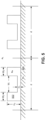
- edge wave or nanojet beam wave element that is used in the dual system illustrated in FIG. 4 is described below with reference to FIG. 5 .
- the base pattern consists in a block 502 of single material having a refractive index n H and having a U shape, placed on top of a substrate 504 having refractive index n 2 .
- the block 502 has two blocks of single material having a refractive index n H of height H 2 and width W 2 separated by a band of same single material having a refractive index n H of height H 1 and width W 1 .
- Such a base pattern is placed in a host medium with refractive index n L , for instance air.
- n H single material may be deposited and e-beamed on a glass substrate ME3. There is no glass etching required, and no multiple e- beam lithography, thus providing potential advantages for the micro-fabrication.
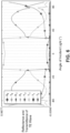
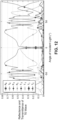
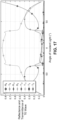
- FIG. 6 illustrates the simulated diffraction performances of the in-coupler grating for the first waveguide WG1. It can be seen that ⁇ 2 diffraction orders have high efficiency and high uniformity for the angular ranges [-72, -30] and [30,72] degrees and it has very high transmission efficiency for ⁇ 30 degrees field of view.
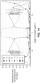
- FIG. 7 illustrates the performances for the grating of the second waveguide WG2. It can be seen that for the transmitted field of view of ⁇ 30 degrees through the grating of the first waveguide WG1, very high diffraction efficiencies and uniformities over this angular range is achieved.
- Some embodiments use a symmetrical U-shaped meta-element combining two similar dielectric blocks with refractive index n H , width W 2 and height H 2 .
- a third block with the refractive index n H , width W 1 and height H 1 is placed between (see FIG. 8A ) and n L is the refractive index of the host medium (e.g. air), with n H ⁇ n 2 ⁇ n H .
- the host medium e.g. air
- four nanojets are associated with two external and two internal edges of the blocks with the height H 2 . Nanojets generated by the internal edges of the system are indicated by NJ int , and nanojets generated by the external edges of the system are indicated by NJ ext .
- the radiation angles of all nanojets are the same ( ⁇ B ).
- the existence of two additional internal edges leads to the decrease of the intensity of the central nanojet (in a case of normal incidence we observe it along the axis of the symmetry of single block meta-elements with the total width W 1 + 2 W 2 and height H 2 ) and to the increase of the intensity of the side blocks.
- the reflection of the generated nanojets (NJ int,r and NJ ext,r ) by the edges of the constitutive parts of the meta-elements leads to the creation of the new nanojet hot spots (cross points between NJ int,r and NJ ext , see FIGs. 8B and 8C and between NJ ext,r and NJ int , see FIG. 8C ) in some proximity to the substrate and to nonsymmetrical redistribution of the total power inside the meta-elements.
- FIGs. 8B and 8C demonstrates the effect of the angles of electromagnetic wave incidence on the nanojets generated at the angles ⁇ B ′ due to the reflection by the different edges of the system.
- Example embodiments as shown above can suppress ⁇ 1 diffraction orders and dramatically increase the intensities of ⁇ 2 diffraction orders for small angles of incidence and decrease them for high angles of incidence.
- the U-shaped topology may improve the diffraction uniformity.
- n H of the elements of the diffraction grating With appropriate selection of the refractive index n H of the elements of the diffraction grating and appropriately selecting the size of these elements, it is possible to increase the intensity of coupling into the corresponding waveguides.
- an optical device providing a high field of view for an RGB image.
- the waveguides disclosed above for a full RGB system.
- example embodiments provide a full RGB system using four waveguides instead of six.
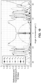
- FIG. 10 shows schematically an exemplary RGB system according to the present embodiment.
- the four waveguides (WG1-WG4) are presented starting from the waveguide WG1.
- As an input there is an RGB image with a field of view of 144 degrees in each color red, green, blue and the three colors are superimposed.
- the waveguides are shown disjointed in order to illustrate the difference in behavior of each color.
- the four waveguides are placed on top of each other, but not in contact.
- a distance of at least some nm, for example 15nm or greater, may be used.
- FIG. 10 shows (row R1) the input field of view per color, and the second row (R2) shows the angular space in each color that gets coupled into the first waveguide WG1.
- the next row (R3) shows the angular space that is transmitted through the waveguide WG1 for each color.
- the illustrations show again (R4) the angular space that is coupled into that waveguide, and so on down to the last one. It is seen that four waveguides can couple a very wide field of view of 144 degrees by multiplexing different combination of colors and angular space.
- the grating for the first waveguide (WG1) is configured for the blue color to get high diffraction efficiency of ⁇ 2 diffraction orders in the angular ranges of [30, 72] and [-72, -30] degrees.
- such a diffraction grating provides high diffraction efficiency for ⁇ 2 diffraction orders in the angular ranges [-72, -48.5] and [48.5, 72] degrees and high transmittivity of 0-order at [-48.5, 48.5] degrees.
- the red color gets through the diffraction grating with high transmittivity of 0 order.
- this diffraction grating provides high diffraction efficiency of ⁇ 2nd diffraction orders in the angular ranges [-72, -33.1] and [33.1, 72] degrees and high transmittivity of 0-order at [-33.1, 33.1] degrees.
- this diffraction grating provides high diffraction efficiency of ⁇ 2 diffraction orders in the angular ranges [-52.5, -15.9] and [15.9, 82.5] degrees and high transmittivity of 0-order at [-15.9, 15.9] degrees.
- d 1 ⁇ d 2 ⁇ d 3 ⁇ d 4 In some embodiments using a stack of four waveguides, d 1 ⁇ d 2 ⁇ d 3 ⁇ d 4 .
- FIG. 11 illustrates the diffraction performances for the blue color in the first waveguide WG1.
- FIG. 12 illustrates the diffraction performances for the blue color in the second waveguide WG2.
- FIG. 13 illustrates the diffraction performances for the green color in the first waveguide WG1.
- FIG. 14 illustrates the diffraction performances for the green color in the second waveguide WG2.
- FIG. 15 illustrates the diffraction performances for the green color in the third waveguide WG3.
- FIG. 16 illustrates the diffraction performances for the red color in the first waveguide WG1.
- FIG. 17 illustrates the diffraction performances for the red color in the second waveguide WG2.
- FIG. 18 illustrates the diffraction performances for the red color in the third waveguide WG3.
- FIG. 19 illustrates the diffraction performances for the red color in the fourth waveguide WG4.
- the smallest pitch size is of 467nm for the first waveguide WG1 is bigger than the blue wavelength.
- use of ⁇ 1 diffraction orders for the blue color would call for a grating pitch smaller than 300nm.
- the use of a U-shaped structure exhibiting edge wave effects to configure the gratings for the ⁇ 2 order of diffraction permits the use of grating periods that are substantially bigger.
- FIG. 20 illustrates a portion of an exemplary diffraction grating as may be used in one or more of the waveguides disclosed above.
- the base pattern of the diffraction grating has a U-shape structure as illustrated in FIG. 5 .
- the optical device according to any one of the embodiments disclosed above can be used as waveguides in AR/VR glasses.
- the waveguides can be configured for in-coupling light incoming into the optical device or for extracting light out of the optical device depending on where the diffraction grating is formed on the waveguides.
- an eyewear apparatus which comprises an optical device according to any one of the embodiments disclosed above.
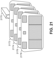
- a monocular or binocular waveguide display as illustrated in FIG. 1C may include a stack of two or more waveguides as illustrated in FIG. 1D .
- an image generator 2170 may provide an image that is coupled into waveguides 2172, 2174, 2176, 2178.
- the in-coupler of waveguide 2172 may be configured as described above for WG1 in FIG. 10 .
- the in-coupler of waveguide 2174 may be configured as described above for WG2 in FIG. 10 .
- the in-coupler of waveguide 2176 may be configured as described above for WG3 in FIG. 10 .
- the in-coupler of waveguide 2178 may be configured as described above for WG4 in FIG. 10 .
- two sets of image generators and accompanying waveguides may be used to provide a stereoscopic display in a set of AR or VR glasses.
- modifiers such as “first,” “second,” “third,” and the like are sometimes used to distinguish different features. These modifiers are not meant to imply any particular order of operation or arrangement of components. Moreover, the terms “first,” “second,” “third,” and the like may have different meanings in different embodiments. For example, a component that is the “first” component in one embodiment may be the “second” component in a different embodiment.
Landscapes
- Physics & Mathematics (AREA)
- General Physics & Mathematics (AREA)
- Optics & Photonics (AREA)
- Engineering & Computer Science (AREA)
- Microelectronics & Electronic Packaging (AREA)
- Diffracting Gratings Or Hologram Optical Elements (AREA)
- Optical Couplings Of Light Guides (AREA)
Claims (15)
- Optische Vorrichtung, umfassend:einen ersten Wellenleiter (WG1) mit einem ersten diffraktiven Einkoppler, wobei der erste diffraktive Einkoppler dafür konfiguriert ist, einen ersten Winkelbereich einfallenden Lichts in negative Richtung in den ersten Wellenleiter einzukoppeln, einen zweiten Winkelbereich einfallenden Lichts in positive Richtung in den ersten Wellenleiter einzukoppeln, wobei der erste und der zweite Winkelbereich sich nicht überlappen, und mindestens einen Teil des nicht in den ersten Wellenleiter eingekoppelten einfallenden Lichts zu übertragen; undeinen zweiten Wellenleiter (WG2) mit einem zweiten diffraktiven Einkoppler, wobei der zweite diffraktive Einkoppler dafür konfiguriert ist, mindestens einen Teil des durch den ersten diffraktiven Einkoppler übertragenen einfallenden Lichts einzukoppeln, wobei der zweite Wellenleiter dafür konfiguriert ist, einen dritten Winkelbereich des einfallenden Lichts einzukoppeln, wobei der dritte Winkelbereich Winkel zwischen dem ersten Winkelbereich und dem zweiten Winkelbereich einschließt.
- Optische Vorrichtung nach Anspruch 1, wobei:
der dritte Winkelbereich einen Bereich von Winkeln zwischen


- Optische Vorrichtung nach Anspruch 2, wobei der erste Winkelbereich einen Bereich von Winkeln kleiner als


- Optische Vorrichtung nach einem der vorstehenden Ansprüche, wobei der erste, der zweite und der dritte Winkelbereich gemeinsam ein Sichtfeld von mehr als sechzig Grad aufspannen.
- Optische Vorrichtung nach einem der vorstehenden Ansprüche, wobei der erste diffraktive Einkoppler eine erste Gitterteilung, d 1, aufweist und dafür konfiguriert ist, eine diffraktive Ordnung M zu nutzen, und wobei d 1/M kleiner als 380 nm ist; und
der zweite diffraktive Einkoppler eine zweite Gitterteilung, d 2, aufweist und dafür konfiguriert ist, eine diffraktive Ordnung N zu nutzen und wobei d 2/N kleiner als 460 nm ist. - Optische Vorrichtung nach einem der vorstehenden Ansprüche, wobei:der erste diffraktive Einkoppler eine erste Gitterteilung, d 1, aufweist, wobei die erste Gitterteilung innerhalb von 20 % von 635 nm liegt; undder zweite diffraktive Einkoppler eine zweite Gitterteilung, d 2, aufweist, wobei die zweite Gitterteilung innerhalb von 20 % von 822 nm liegt.
- Optische Vorrichtung nach einem der vorstehenden Ansprüche, wobei der zweite diffraktive Einkoppler eine zweite Gitterteilung, d 2, aufweist, die zwischen 1,2-mal und 1,4-mal größer als eine erste Gitterteilung, d 1, des ersten diffraktiven Einkopplers ist.
- Optische Vorrichtung nach einem der vorstehenden Ansprüche, wobei mindestens einer des ersten und des zweiten diffraktiven Einkopplers ein Basismuster mit einem U-förmigen Profil aufweist.
- Optische Vorrichtung nach einem der vorstehenden Ansprüche, ferner umfassend:einen Bildgenerator, der dazu dient, Licht, das ein Bild repräsentiert, auf den ersten diffraktiven Einkoppler zu richten;einen ersten diffraktiven Auskoppler auf dem ersten Wellenleiter; undeinen zweiten diffraktiven Auskoppler auf dem zweiten Wellenleiter.
- Verfahren, umfassend:Richten von einfallendem Licht auf einen ersten diffraktiven Einkoppler eines ersten Wellenleiters (WG1);Einkoppeln, durch den ersten diffraktiven Einkoppler, eines ersten Winkelbereichs und eines zweiten Winkelbereichs des einfallenden Lichts in den ersten Wellenleiter, wobei der erste und der zweite Wellenbereich sich nicht überlappen, wobei der erste Winkelbereich in negative Richtung in den ersten Wellenleiter eingekoppelt wird und der zweite Winkelbereich in positive Richtung in den ersten Wellenleiter eingekoppelt wird;Übertragen, durch den ersten diffraktiven Einkoppler an einen zweiten diffraktiven Einkoppler eines zweiten Wellenleiters (WG2), von mindestens einem Teil des einfallenden Lichts, das nicht in den ersten Wellenleiter eingekoppelt wird, undEinkoppeln, durch den zweiten diffraktiven Einkoppler, eines dritten Winkelbereichs des einfallenden Lichts, wobei der dritte Winkelbereich Winkel zwischen dem ersten Winkelbereich und dem zweiten Winkelbereich einschließt.
- Verfahren nach Anspruch 10, wobei:
der dritte Winkelbereich einen Bereich von Winkeln zwischen


- Verfahren nach Anspruch 11, wobei der erste Winkelbereich einen Bereich von Winkeln kleiner als


- Verfahren nach einem der Ansprüche 10-12, wobei der erste, der zweite und der dritte Winkelbereich gemeinsam ein Sichtfeld von mehr als sechzig Grad aufspannen.
- Verfahren nach einem der Ansprüche 10-13, wobei:der erste diffraktive Einkoppler eine erste Gitterteilung, d1, aufweist, wobei die erste Gitterteilung innerhalb von 20 % von 635 nm liegt; undder zweite diffraktive Einkoppler eine zweite Gitterteilung, d2, aufweist, wobei die zweite Gitterteilung innerhalb von 20 % von 822 nm liegt.
- Verfahren nach einem der Ansprüche 10-14, wobei der zweite diffraktive Einkoppler eine zweite Gitterteilung, d2, aufweist, die zwischen 1,2-mal und 1,4-mal größer als eine erste Gitterteilung, d1, des ersten diffraktiven Einkopplers ist.
Applications Claiming Priority (2)
| Application Number | Priority Date | Filing Date | Title |
|---|---|---|---|
| EP19198478 | 2019-09-19 | ||
| PCT/EP2020/076173 WO2021053182A1 (en) | 2019-09-19 | 2020-09-18 | Optical device for coupling a high field of view of incident light |
Publications (2)
| Publication Number | Publication Date |
|---|---|
| EP4031927A1 EP4031927A1 (de) | 2022-07-27 |
| EP4031927B1 true EP4031927B1 (de) | 2024-10-30 |
Family
ID=68158869
Family Applications (1)
| Application Number | Title | Priority Date | Filing Date |
|---|---|---|---|
| EP20771595.4A Active EP4031927B1 (de) | 2019-09-19 | 2020-09-18 | Optische vorrichtung zum koppeln eines hohen blickfeldes von einfallendem licht |
Country Status (4)
| Country | Link |
|---|---|
| US (1) | US20220357579A1 (de) |
| EP (1) | EP4031927B1 (de) |
| CN (1) | CN114710965A (de) |
| WO (1) | WO2021053182A1 (de) |
Families Citing this family (16)
| Publication number | Priority date | Publication date | Assignee | Title |
|---|---|---|---|---|
| EP3540499A1 (de) | 2018-03-13 | 2019-09-18 | Thomson Licensing | Bildsensor mit einem farbteiler mit zwei verschiedenen brechungsindizes |
| EP3540479A1 (de) | 2018-03-13 | 2019-09-18 | Thomson Licensing | Beugungsgitter mit doppelmaterialstrukturen |
| EP3588150A1 (de) | 2018-06-29 | 2020-01-01 | Thomson Licensing | Optische vorrichtung mit mehrschichtigen wellenleitern |
| EP3591700A1 (de) | 2018-07-02 | 2020-01-08 | Thomson Licensing | Bildsensor mit einem farbteiler mit zwei verschiedenen brechungsindizes und unterschiedlicher höhe |
| EP3671322A1 (de) | 2018-12-18 | 2020-06-24 | Thomson Licensing | Vorrichtung zur formung einer ausgehenden elektromagnetischen welle aus einer einfallenden elektromagnetischen welle |
| EP3671310A1 (de) | 2018-12-18 | 2020-06-24 | Thomson Licensing | Optische manipulationsvorrichtung zum einfangen oder bewegen von mikro- oder nanopartikeln |
| EP3671293A1 (de) | 2018-12-21 | 2020-06-24 | Thomson Licensing | Optische vorrichtung mit mindestens einem beugungsgitter mit einem gitterpegel über der wellenlänge |
| EP4127820A1 (de) | 2020-03-23 | 2023-02-08 | InterDigital CE Patent Holdings, SAS | Wellenleiteranzeigesystem mit breitem sichtfeld |
| CN116324587A (zh) | 2020-08-13 | 2023-06-23 | 交互数字Ce专利控股有限公司 | 通过c形平面光学架构的低失真成像 |
| US20240264354A1 (en) * | 2021-06-10 | 2024-08-08 | Interdigital Ce Patent Holdings, Sas | Dual diffraction grating in-coupler for reduced waveguide thickness background |
| EP4359846A1 (de) * | 2021-06-25 | 2024-05-01 | InterDigital CE Patent Holdings, SAS | Leckagenunterdrückung für austrittspupillenexpander |
| JP7748679B2 (ja) | 2021-09-22 | 2025-10-03 | Cellid株式会社 | 投影基板及び眼鏡型端末 |
| CN114637116B (zh) * | 2022-03-15 | 2023-02-10 | 嘉兴驭光光电科技有限公司 | 衍射光波导以及具有其的显示设备 |
| US12393029B2 (en) * | 2022-03-23 | 2025-08-19 | Adeia Guides Inc. | Buried diffractive gratings for optical elements of augmented reality and virtual reality head-mounted displays |
| US12504566B2 (en) | 2022-05-16 | 2025-12-23 | Adeia Guides Inc. | Transparent conductive diffractive gratings for optical elements of augmented reality and virtual reality displays |
| JPWO2023203600A1 (de) * | 2022-04-18 | 2023-10-26 |
Family Cites Families (12)
| Publication number | Priority date | Publication date | Assignee | Title |
|---|---|---|---|---|
| GB201114149D0 (en) * | 2011-08-17 | 2011-10-05 | Bae Systems Plc | Projection display |
| GB2529003B (en) * | 2014-08-03 | 2020-08-26 | Wave Optics Ltd | Optical device |
| JP6608065B2 (ja) * | 2016-01-06 | 2019-11-20 | ビュージックス コーポレーション | ダイクロイックフィルタを埋め込んだ両面型のイメージング光ガイド |
| US9791703B1 (en) | 2016-04-13 | 2017-10-17 | Microsoft Technology Licensing, Llc | Waveguides with extended field of view |
| US10061124B2 (en) * | 2016-04-29 | 2018-08-28 | Microsoft Technology Licensing, Llc | Robust architecture for large field of view components |
| US9939647B2 (en) * | 2016-06-20 | 2018-04-10 | Microsoft Technology Licensing, Llc | Extended field of view in near-eye display using optically stitched imaging |
| WO2018039277A1 (en) * | 2016-08-22 | 2018-03-01 | Magic Leap, Inc. | Diffractive eyepiece |
| US10371896B2 (en) * | 2016-12-22 | 2019-08-06 | Magic Leap, Inc. | Color separation in planar waveguides using dichroic filters |
| CN110462487B (zh) * | 2017-03-21 | 2022-07-01 | 奇跃公司 | 用于组合视场的具有不同衍射光栅的堆叠波导 |
| FI129113B (en) * | 2017-12-22 | 2021-07-15 | Dispelix Oy | Waveguide display and display element with new lattice configuration |
| CN108681067A (zh) * | 2018-05-16 | 2018-10-19 | 上海鲲游光电科技有限公司 | 一种扩展视场角的波导显示装置 |
| EP3671293A1 (de) | 2018-12-21 | 2020-06-24 | Thomson Licensing | Optische vorrichtung mit mindestens einem beugungsgitter mit einem gitterpegel über der wellenlänge |
-
2020
- 2020-09-18 CN CN202080070747.8A patent/CN114710965A/zh active Pending
- 2020-09-18 US US17/761,002 patent/US20220357579A1/en active Pending
- 2020-09-18 WO PCT/EP2020/076173 patent/WO2021053182A1/en not_active Ceased
- 2020-09-18 EP EP20771595.4A patent/EP4031927B1/de active Active
Also Published As
| Publication number | Publication date |
|---|---|
| CN114710965A (zh) | 2022-07-05 |
| WO2021053182A1 (en) | 2021-03-25 |
| US20220357579A1 (en) | 2022-11-10 |
| EP4031927A1 (de) | 2022-07-27 |
Similar Documents
| Publication | Publication Date | Title |
|---|---|---|
| EP4031927B1 (de) | Optische vorrichtung zum koppeln eines hohen blickfeldes von einfallendem licht | |
| US12228756B2 (en) | Optical device | |
| CN115857100B (zh) | 在一块板上支持红色、绿色和蓝色的大视场波导 | |
| EP4133325B1 (de) | Wellenleiteranzeige mit kreuzpolarisierten augenpupillenexpandierern | |
| CN112817153A (zh) | 一种大视场角的光学扩瞳装置、显示装置及方法 | |
| JP2017156388A (ja) | 光束径拡大素子及び画像表示装置 | |
| US12326562B2 (en) | Waveguide display system with wide field of view | |
| EP4127789B1 (de) | Unpolarisiertes lichtgitter in einem koppler | |
| US20230400618A1 (en) | Single mode full color waveguide combiner using asymmetric transmissive and reflective diffraction gratings | |
| US12449583B2 (en) | Low distortion imaging through a C-shape flat optical architecture | |
| WO2023061919A1 (en) | Full color eye-pupil-expanders with high vertical field of view | |
| WO2022008378A1 (en) | Reflective in-coupler design with high refractive index element using second diffraction order for near-eye displays | |
| KR20220047159A (ko) | 증강현실장치용 도파로의 회절광학소자 아키텍처 | |
| EP4191293A1 (de) | Wellenleiter-anzeigegerät | |
| EP4176302B1 (de) | Vollfarbiger wellenleiterkombinierer mit eingebetteter metagitterung | |
| US20240094537A1 (en) | Uniform incoupler for conical incidence | |
| CN114839765A (zh) | 一种大视场角的光学扩瞳装置、显示装置及方法 | |
| EP4154043B1 (de) | Doppelmaterialbeugungsgitter mit hoher farbuniformität und stufenförmigen hohlräumen |
Legal Events
| Date | Code | Title | Description |
|---|---|---|---|
| STAA | Information on the status of an ep patent application or granted ep patent |
Free format text: STATUS: UNKNOWN |
|
| STAA | Information on the status of an ep patent application or granted ep patent |
Free format text: STATUS: THE INTERNATIONAL PUBLICATION HAS BEEN MADE |
|
| PUAI | Public reference made under article 153(3) epc to a published international application that has entered the european phase |
Free format text: ORIGINAL CODE: 0009012 |
|
| STAA | Information on the status of an ep patent application or granted ep patent |
Free format text: STATUS: REQUEST FOR EXAMINATION WAS MADE |
|
| 17P | Request for examination filed |
Effective date: 20220322 |
|
| AK | Designated contracting states |
Kind code of ref document: A1 Designated state(s): AL AT BE BG CH CY CZ DE DK EE ES FI FR GB GR HR HU IE IS IT LI LT LU LV MC MK MT NL NO PL PT RO RS SE SI SK SM TR |
|
| DAV | Request for validation of the european patent (deleted) | ||
| DAX | Request for extension of the european patent (deleted) | ||
| RAP1 | Party data changed (applicant data changed or rights of an application transferred) |
Owner name: INTERDIGITAL MADISON PATENT HOLDINGS, SAS |
|
| RIC1 | Information provided on ipc code assigned before grant |
Ipc: F21V 8/00 20060101ALI20240506BHEP Ipc: G02B 27/01 20060101ALI20240506BHEP Ipc: G02B 27/00 20060101AFI20240506BHEP |
|
| GRAP | Despatch of communication of intention to grant a patent |
Free format text: ORIGINAL CODE: EPIDOSNIGR1 |
|
| GRAP | Despatch of communication of intention to grant a patent |
Free format text: ORIGINAL CODE: EPIDOSNIGR1 |
|
| STAA | Information on the status of an ep patent application or granted ep patent |
Free format text: STATUS: GRANT OF PATENT IS INTENDED |
|
| INTG | Intention to grant announced |
Effective date: 20240614 |
|
| GRAS | Grant fee paid |
Free format text: ORIGINAL CODE: EPIDOSNIGR3 |
|
| P01 | Opt-out of the competence of the unified patent court (upc) registered |
Free format text: CASE NUMBER: APP_48182/2024 Effective date: 20240821 |
|
| GRAA | (expected) grant |
Free format text: ORIGINAL CODE: 0009210 |
|
| STAA | Information on the status of an ep patent application or granted ep patent |
Free format text: STATUS: THE PATENT HAS BEEN GRANTED |
|
| AK | Designated contracting states |
Kind code of ref document: B1 Designated state(s): AL AT BE BG CH CY CZ DE DK EE ES FI FR GB GR HR HU IE IS IT LI LT LU LV MC MK MT NL NO PL PT RO RS SE SI SK SM TR |
|
| REG | Reference to a national code |
Ref country code: GB Ref legal event code: FG4D |
|
| REG | Reference to a national code |
Ref country code: CH Ref legal event code: EP |
|
| REG | Reference to a national code |
Ref country code: DE Ref legal event code: R096 Ref document number: 602020040359 Country of ref document: DE |
|
| REG | Reference to a national code |
Ref country code: IE Ref legal event code: FG4D |
|
| REG | Reference to a national code |
Ref country code: LT Ref legal event code: MG9D |
|
| REG | Reference to a national code |
Ref country code: NL Ref legal event code: MP Effective date: 20241030 |
|
| PG25 | Lapsed in a contracting state [announced via postgrant information from national office to epo] |
Ref country code: PT Free format text: LAPSE BECAUSE OF FAILURE TO SUBMIT A TRANSLATION OF THE DESCRIPTION OR TO PAY THE FEE WITHIN THE PRESCRIBED TIME-LIMIT Effective date: 20250228 Ref country code: HR Free format text: LAPSE BECAUSE OF FAILURE TO SUBMIT A TRANSLATION OF THE DESCRIPTION OR TO PAY THE FEE WITHIN THE PRESCRIBED TIME-LIMIT Effective date: 20241030 Ref country code: IS Free format text: LAPSE BECAUSE OF FAILURE TO SUBMIT A TRANSLATION OF THE DESCRIPTION OR TO PAY THE FEE WITHIN THE PRESCRIBED TIME-LIMIT Effective date: 20250228 |
|
| PG25 | Lapsed in a contracting state [announced via postgrant information from national office to epo] |
Ref country code: FI Free format text: LAPSE BECAUSE OF FAILURE TO SUBMIT A TRANSLATION OF THE DESCRIPTION OR TO PAY THE FEE WITHIN THE PRESCRIBED TIME-LIMIT Effective date: 20241030 Ref country code: NL Free format text: LAPSE BECAUSE OF FAILURE TO SUBMIT A TRANSLATION OF THE DESCRIPTION OR TO PAY THE FEE WITHIN THE PRESCRIBED TIME-LIMIT Effective date: 20241030 |
|
| REG | Reference to a national code |
Ref country code: AT Ref legal event code: MK05 Ref document number: 1737447 Country of ref document: AT Kind code of ref document: T Effective date: 20241030 |
|
| PG25 | Lapsed in a contracting state [announced via postgrant information from national office to epo] |
Ref country code: BG Free format text: LAPSE BECAUSE OF FAILURE TO SUBMIT A TRANSLATION OF THE DESCRIPTION OR TO PAY THE FEE WITHIN THE PRESCRIBED TIME-LIMIT Effective date: 20241030 |
|
| PG25 | Lapsed in a contracting state [announced via postgrant information from national office to epo] |
Ref country code: ES Free format text: LAPSE BECAUSE OF FAILURE TO SUBMIT A TRANSLATION OF THE DESCRIPTION OR TO PAY THE FEE WITHIN THE PRESCRIBED TIME-LIMIT Effective date: 20241030 |
|
| PG25 | Lapsed in a contracting state [announced via postgrant information from national office to epo] |
Ref country code: NO Free format text: LAPSE BECAUSE OF FAILURE TO SUBMIT A TRANSLATION OF THE DESCRIPTION OR TO PAY THE FEE WITHIN THE PRESCRIBED TIME-LIMIT Effective date: 20250130 |
|
| PG25 | Lapsed in a contracting state [announced via postgrant information from national office to epo] |
Ref country code: LV Free format text: LAPSE BECAUSE OF FAILURE TO SUBMIT A TRANSLATION OF THE DESCRIPTION OR TO PAY THE FEE WITHIN THE PRESCRIBED TIME-LIMIT Effective date: 20241030 Ref country code: GR Free format text: LAPSE BECAUSE OF FAILURE TO SUBMIT A TRANSLATION OF THE DESCRIPTION OR TO PAY THE FEE WITHIN THE PRESCRIBED TIME-LIMIT Effective date: 20250131 Ref country code: AT Free format text: LAPSE BECAUSE OF FAILURE TO SUBMIT A TRANSLATION OF THE DESCRIPTION OR TO PAY THE FEE WITHIN THE PRESCRIBED TIME-LIMIT Effective date: 20241030 |
|
| PG25 | Lapsed in a contracting state [announced via postgrant information from national office to epo] |
Ref country code: PL Free format text: LAPSE BECAUSE OF FAILURE TO SUBMIT A TRANSLATION OF THE DESCRIPTION OR TO PAY THE FEE WITHIN THE PRESCRIBED TIME-LIMIT Effective date: 20241030 |
|
| PG25 | Lapsed in a contracting state [announced via postgrant information from national office to epo] |
Ref country code: RS Free format text: LAPSE BECAUSE OF FAILURE TO SUBMIT A TRANSLATION OF THE DESCRIPTION OR TO PAY THE FEE WITHIN THE PRESCRIBED TIME-LIMIT Effective date: 20250130 |
|
| PG25 | Lapsed in a contracting state [announced via postgrant information from national office to epo] |
Ref country code: SM Free format text: LAPSE BECAUSE OF FAILURE TO SUBMIT A TRANSLATION OF THE DESCRIPTION OR TO PAY THE FEE WITHIN THE PRESCRIBED TIME-LIMIT Effective date: 20241030 |
|
| PG25 | Lapsed in a contracting state [announced via postgrant information from national office to epo] |
Ref country code: DK Free format text: LAPSE BECAUSE OF FAILURE TO SUBMIT A TRANSLATION OF THE DESCRIPTION OR TO PAY THE FEE WITHIN THE PRESCRIBED TIME-LIMIT Effective date: 20241030 |
|
| PG25 | Lapsed in a contracting state [announced via postgrant information from national office to epo] |
Ref country code: EE Free format text: LAPSE BECAUSE OF FAILURE TO SUBMIT A TRANSLATION OF THE DESCRIPTION OR TO PAY THE FEE WITHIN THE PRESCRIBED TIME-LIMIT Effective date: 20241030 |
|
| PG25 | Lapsed in a contracting state [announced via postgrant information from national office to epo] |
Ref country code: RO Free format text: LAPSE BECAUSE OF FAILURE TO SUBMIT A TRANSLATION OF THE DESCRIPTION OR TO PAY THE FEE WITHIN THE PRESCRIBED TIME-LIMIT Effective date: 20241030 |
|
| PG25 | Lapsed in a contracting state [announced via postgrant information from national office to epo] |
Ref country code: SK Free format text: LAPSE BECAUSE OF FAILURE TO SUBMIT A TRANSLATION OF THE DESCRIPTION OR TO PAY THE FEE WITHIN THE PRESCRIBED TIME-LIMIT Effective date: 20241030 |
|
| PG25 | Lapsed in a contracting state [announced via postgrant information from national office to epo] |
Ref country code: CZ Free format text: LAPSE BECAUSE OF FAILURE TO SUBMIT A TRANSLATION OF THE DESCRIPTION OR TO PAY THE FEE WITHIN THE PRESCRIBED TIME-LIMIT Effective date: 20241030 |
|
| PG25 | Lapsed in a contracting state [announced via postgrant information from national office to epo] |
Ref country code: IT Free format text: LAPSE BECAUSE OF FAILURE TO SUBMIT A TRANSLATION OF THE DESCRIPTION OR TO PAY THE FEE WITHIN THE PRESCRIBED TIME-LIMIT Effective date: 20241030 |
|
| REG | Reference to a national code |
Ref country code: DE Ref legal event code: R097 Ref document number: 602020040359 Country of ref document: DE |
|
| PLBE | No opposition filed within time limit |
Free format text: ORIGINAL CODE: 0009261 |
|
| STAA | Information on the status of an ep patent application or granted ep patent |
Free format text: STATUS: NO OPPOSITION FILED WITHIN TIME LIMIT |
|
| PG25 | Lapsed in a contracting state [announced via postgrant information from national office to epo] |
Ref country code: SE Free format text: LAPSE BECAUSE OF FAILURE TO SUBMIT A TRANSLATION OF THE DESCRIPTION OR TO PAY THE FEE WITHIN THE PRESCRIBED TIME-LIMIT Effective date: 20241030 |
|
| 26N | No opposition filed |
Effective date: 20250731 |
|
| PGFP | Annual fee paid to national office [announced via postgrant information from national office to epo] |
Ref country code: DE Payment date: 20250926 Year of fee payment: 6 |
|
| PGFP | Annual fee paid to national office [announced via postgrant information from national office to epo] |
Ref country code: FR Payment date: 20250925 Year of fee payment: 6 |