EP4154043B1 - Doppelmaterialbeugungsgitter mit hoher farbuniformität und stufenförmigen hohlräumen - Google Patents
Doppelmaterialbeugungsgitter mit hoher farbuniformität und stufenförmigen hohlräumen Download PDFInfo
- Publication number
- EP4154043B1 EP4154043B1 EP21727442.2A EP21727442A EP4154043B1 EP 4154043 B1 EP4154043 B1 EP 4154043B1 EP 21727442 A EP21727442 A EP 21727442A EP 4154043 B1 EP4154043 B1 EP 4154043B1
- Authority
- EP
- European Patent Office
- Prior art keywords
- refractive index
- substrate
- waveguide
- diffraction grating
- grating
- Prior art date
- Legal status (The legal status is an assumption and is not a legal conclusion. Google has not performed a legal analysis and makes no representation as to the accuracy of the status listed.)
- Active
Links
Images


Classifications
-
- G—PHYSICS
- G02—OPTICS
- G02B—OPTICAL ELEMENTS, SYSTEMS OR APPARATUS
- G02B5/00—Optical elements other than lenses
- G02B5/18—Diffraction gratings
-
- G—PHYSICS
- G02—OPTICS
- G02B—OPTICAL ELEMENTS, SYSTEMS OR APPARATUS
- G02B5/00—Optical elements other than lenses
- G02B5/18—Diffraction gratings
- G02B5/1847—Manufacturing methods
Definitions
- the present disclosure relates to the field of optics and photonics, and more specifically to optical device comprising at least one diffraction grating. It may find applications in the field of conformable and wearable optics (e.g. ARNR glasses (Augmented RealityNirtual Reality)), as well as in a variety of other electronic consumer products comprising displays and/or lightweight imaging systems, including head up displays (HUD), as for example in the automotive industry.
- ARNR glasses Augmented RealityNirtual Reality
- HUD head up displays
- planar lens thanks to its small thickness and excellent focusing capability, has been developed to replace its thicker dielectric counterpart as a paradigmatic nanophotonic component.
- planar lenses have been studied so far, for example zone plates, nano-slit and nano-hole arrays, photonics crystals and metasurfaces.
- different terminologies are used in the aforementioned techniques, they share the same principle of focusing, which is to generate a constructive interference at the focal point by curving the phase front of an incident plane wave.
- the focusing (or beam forming) of electromagnetic waves is an established way to increase locally the magnitude of the electric field and, in such a way, to enhance efficiency of sensors, e.g. electro-optical sensors whose operational principles rely on the conversion of the energy propagating in space in the form of an electromagnetic wave into an output voltage or current.
- planar lenses has been improved through sophisticated designs. However, most of the proposals so far lack the possibility to control the focal spot position or to change the orientation of an electromagnetic beam.
- optical devices which comprise components enabling light focusing and deviating functions.
- digital image sensors used in various photo/video cameras
- optical combiners used in AR/VR glasses
- light guiding systems being the essential part of various light capturing and light processing devices.
- components which are able to perform both functions simultaneously, such as asymmetric dielectric lenses, diffractive lenses and diffractive gratings.
- Transformation Optics allows the possibility of controlling electromagnetic (EM) fields through the use of judiciously engineered materials with parameters that vary spatially. Such flexibility in controlling EM waves appears to be convenient in the design of novel devices with performance or special desired properties that have been difficult to achieve.
- the excitation source transmits through the lens corresponding to the transformed medium, which deflects the beam away from the normal direction.
- the all-dielectric compact low-cost lens prototype presenting a graded permittivity profile was fabricated through three-dimensional (3D) polyjet printing technology.
- the array of radiators was composed of four planar microstrip antennas realized using standard lithography techniques and was used as excitation source for the lens.
- phase front profile is achieved through two mechanisms: phase retardation caused by the width and shape of the individual slits in the lens, and the position of these slits.
- the proposed single-layered lenses can be conveniently fabricated using Focused Ion Beam (FIB) techniques.
- FIB Focused Ion Beam
- Metasurfaces can provide solutions to realize complex optical systems in a compact and planar configuration.
- the off-axis meta-lenses that simultaneously focus and disperse light of different wavelengths with high spectral resolution were presented in M. Khorasaninejad et al., "Super-Dispersive Off-Axis Meta-Lenses for Compact High Resolution Spetrcoscopy” (Nano Lett., Vol. 16, No. 6, 3732 (2016 )). They are designed based on the geometric phase via rotated silicon nanofins and can focus light at angles as large as 80°.
- a planar metalens that consists of an array of slits that are filled with phase-change material Ge 2 SB 2 Te 5 (GST) has also been proposed to engineer the far-field focusing patterns in " Engineering the phase front of light with phase-change material based planar lenses" by Y. Chen et al (Sci. Rep., Vol. 5, Article number: 8660 (2015 )).
- a photonic nanojet is a narrow high-intensity optical radiation flux formed in the proximity to the shadow surface of illuminated transparent dielectric symmetric bodies with a diameter comparable to or somewhat larger than the wavelength of the incident optical radiation.
- the physical origin of photonic nanojet formation arises from the interference (both constructive and destructive) of the radiation net fluxes diffracted and passed through a particle (see for example " Photonic nanojet-enabled optical data storage by S.-C. Kong et al. (Opt. Express, Vol. 16, No.
- patent document US 7 394 535 " Terajets produced by dielectric cuboids" by V. Pacheco-Pena et al. (Applied Phys. Lett., Vol. 105, 084102, 2014 ) and " Multifrequency focusing and wide angular scanning of terajets" by V. Pacheco-Pena et al. (Opt. Lett. Vol. 40, No. 2, pp. 245-248, 2015 )).
- photonic nanojets One feature of photonic nanojets is the high spatial localization of the light field in the longitudinal direction (relative to the direction of incidence), which, in contrast to conventional high-NA (Numerical Aperture) focusing optics, can lead to the subwavelength dimensions of the photonic jet.
- the common interest to the nanojet effect is mostly caused by the promises of its practical application in nanophotonics, biology, medicine, and nanoelectronics.
- the principles of functioning of some devices are based on the ability of the nanojet to provide the high intensity of the electromagnetic field in a localized spatial region near a microparticle and on high sensitivity to perturbations of both the field and material origin.
- the nanojet is produced by a composite radially inhomogeneous particle consisting of several concentric shells with different refractive indices (see for example " Ultralong photonic nanojet formed by a two-layer dielectric microsphere” by Yu Shen et al. (Opt. Lett., Vol. 39, No. 14, 4120 (2014 ), " Detection of embedded ultra-subwavelength-thin dielectric features using elongated photonic nanojets” by C.M. Riuz et al. (Opt. Express, Vol. 18, No. 16, 16805 (2010 ), " Photonic nanojet calculations in layered radially inhomogeneous micrometer-sized spherical particles” by Yu E.
- ARNR glasses are under consideration for a new generation of human-machine interface.
- Development of AR/VR glasses is associated with a number of challenges, including reduction of size and weight of such devices as well as improvement of the image quality (in terms of contrast, field of view, color depth, etc.) that should be realistic enough to enable a truly immersive user experience.
- optical components The tradeoff between the image quality and physical size of the optical components motivates research into ultra-compact optical components that can be used as building blocks for more complex optical systems, such as ARNR glasses. It is desirable for such optical components to be easy to fabricate and replicate.
- various types of refractive and diffractive lenses and beam-forming components are used to guide the light from a micro-display or a projector towards the human eye, allowing formation of a virtual image that is superimposed with an image of the physical world seen with a naked eye.
- Some of kinds of ARNR glasses utilize an optical waveguide wherein light propagates into the optical waveguide by TIR (for Total Internal Reflection) only over a limited range of internal angles.
- TIR Total Internal Reflection
- the FoV for Field of View
- the material of the waveguide depends on the material of the waveguide, among other factors.
- a waveguide with an extended field of view wherein a dual mode image propagation is used.
- the diffraction mode +1 is used to carry the right hand side image (negative angles of incidence on the in-coupler) in one direction
- the -1 mode is used to propagate the positive angles of incidence into the opposite direction into the waveguide.
- combining both half images is done thanks to the pupil expanders and out-couplers at the exit of the waveguide so that the user sees one single image.
- the goal of the system is to double the field of view since each half image can use the whole angular bandwidth of the waveguide in each direction of propagation.
- diffraction orders higher than one has the effect of multiplying the wavelength by the diffraction order that is used in the diffraction equation.
- the grating pitch is directly a function of the product M ⁇ , this means that the grating pitch is multiplied by M.
- a grating density with fewer lines per millimeter can be used, and the fabrication process can be simplified by using over-wavelength structures rather than sub-wavelength.
- An optical waveguide using both ⁇ 2 diffraction orders provides a FoV of about 60° with a refractive index of 1.52. It is thus possible to get a 60° field of view using a material with refractive index 1.52, instead of 2 in single mode. However, a 60° FoV is still limited with respect to the total human field of view where stereopsis is effective for human vision and which is about 114°.
- Waveguide-based ARNR glasses can exhibit a wide field of view along one direction (e.g. in a horizontal direction) but may have a narrower field of view along another direction (e.g. in a vertical direction).
- ARNR applications generally call for particular aspect ratios
- a limitation of the field of view along one direction may, for practical purposes, effectively limit the field of view along the other direction.
- KR20190073107A also describes diffraction gratings of the prior art.
- references in the specification to "one embodiment,” “an embodiment,” “an example embodiment,” and the like indicate that the embodiment described may include a particular feature, structure, or characteristic; but not every embodiment necessarily includes that particular feature, structure, or characteristic. Moreover, such phrases are not necessarily referring to the same embodiment. Further, when a particular feature, structure, or characteristic is described in connection with an embodiment, such feature, structure, or characteristic may be used in connection with other embodiments whether or not explicitly described.
- a diffraction grating according to claim 1 comprises: a substrate having an outer surface, the substrate having a first refractive index; and a plurality of grating elements, each grating element comprising a stepped channel inset into the substrate, the stepped channel having a second refractive index greater than the first refractive index.
- the stepped channel is a two-step channel having a first step along the outer surface of the substrate and a second step extending inward from the first step, the first step having a greater width than the second step.
- a method of making a diffraction grating according to claim 7 comprises: forming a plurality of stepped channels in an outer surface of a substrate having a first refractive index; and filling each of the stepped channels with a material having a second refractive index greater than the first refractive index.
- Each of the stepped channels is a two-step channel having a first step along the outer surface of the substrate and a second step extending inward from the first step, the first step having a greater width than the second step.
- the stepped channel has an outer surface substantially coplanar with the outer surface of the substrate.
- the width of the first step is substantially twice as great as the width of the second step.
- a side edge of the first step is substantially aligned with a side edge of the second step.
- the height h 2 of the stepped channel is less than twice the height h 1 of the first step.
- the substrate is a waveguide in a waveguide display.
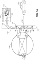
- FIG. 1A is a schematic cross-sectional side view of a waveguide display device in operation.
- An image is projected by an image generator 102.
- the image generator 102 may use one or more of various techniques for projecting an image.
- the image generator 102 may be a laser beam scanning (LBS) projector, a liquid crystal display (LCD), a light-emitting diode (LED) display (including an organic LED (OLED) or micro LED ( ⁇ LED) display), a digital light processor (DLP), a liquid crystal on silicon (LCoS) display, or other type of image generator or light engine.
- LBS laser beam scanning
- LCD liquid crystal display
- LED light-emitting diode
- ⁇ LED micro LED
- DLP digital light processor
- LCDoS liquid crystal on silicon
- Light representing an image 112 generated by the image generator 102 is coupled into a waveguide 104 by a diffractive in-coupler 106.
- the in-coupler 106 diffracts the light representing the image 112 into one or more diffractive orders.
- light ray 108 which is one of the light rays representing a portion of the bottom of the image, is diffracted by the in-coupler 106, and one of the diffracted orders 110 (e.g. the second order) is at an angle that makes it capable of being propagated through the waveguide 104 by total internal reflection.
- At least a portion of the light 110 that has been coupled into the waveguide 104 by the diffractive in-coupler 106 is coupled out of the waveguide by a diffractive out-coupler 114.
- At least some of the light coupled out of the waveguide 104 replicates the incident angle of light coupled into the waveguide.
- out-coupled light rays 116a, 116b, and 116c replicate the angle of the in-coupled light ray 108. Because light exiting the out-coupler replicates the directions of light that entered the in-coupler, the waveguide substantially replicates the original image 112. A user's eye 118 can see the replicated image.
- the out-coupler 114 out-couples only a portion of the light with each reflection allowing a single input beam (such as beam 108) to generate multiple parallel output beams (such as beams 116a, 116b, and 116c). In this way, at least some of the light originating from each portion of the image is likely to reach the user's eye even if the eye is not perfectly aligned with the center of the out-coupler. For example, if the eye 118 were to move downward, beam 116c may enter the eye even if beams 116a and 116b do not, so the user can still perceive the bottom of the image 112 despite the shift in position.
- the out-coupler 114 thus operates in part as an exit pupil expander in the vertical direction.
- the waveguide may also include one or more additional exit pupil expanders (not shown in FIG. 1A ) to expand the exit pupil in the horizontal direction.
- the waveguide 104 is at least partly transparent with respect to light originating outside the waveguide display.
- the light 120 from real-world objects such as object 122 traverses the waveguide 104, allowing the user to see the real-world objects while using the waveguide display.
- the diffraction grating 114 As light 120 from real-world objects also goes through the diffraction grating 114, there will be multiple diffraction orders and hence multiple images.
- the diffraction order zero no deviation by 114 to have a great diffraction efficiency for light 120 and order zero, while higher diffraction orders are lower in energy.
- the out-coupler 114 is preferably configured to let through the zero order of the real image. In such embodiments, images displayed by the waveguide display may appear to be superimposed on the real world.
- a waveguide display includes more than one waveguide layer.
- Each waveguide layer may be configured to preferentially convey light with a particular range of wavelengths and/or incident angles from the image generator to the viewer.
- waveguide displays having in-couplers, out-couplers, and pupil expanders may have various different configurations.
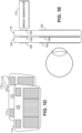
- An example layout of one binocular waveguide display is illustrated in FIG. 1B .
- the display includes waveguides 152a, 152b for the left and right eyes, respectively.
- the waveguides include in-couplers 154a,b, pupil expanders 156a,b, and components 158a,b, which operate as both out-couplers and horizontal pupil expanders.
- the pupil expanders 156a,b are arranged along an optical path between the in-coupler and the out-coupler.
- An image generator (not shown) may be provided for each eye and arranged to project light representing an image on the respective in-coupler.
- FIG.1C An example layout of another binocular waveguide display is illustrated in FIG.1C .
- the display includes waveguides 160a, 160b for the left and right eyes, respectively.
- the waveguides include in-couplers 162a,b. Light from different portions of an image may be coupled by the in-couplers 162a,b to different directions within the waveguides. In-coupled light traveling toward the left passes through pupil expanders 164a,b, while in-coupled light traveling toward the right passes through pupil expanders 166a,b. Having passed through the pupil expanders, light is coupled out of the waveguides using components 168a,b, which operate as both out-couplers and vertical pupil expanders to substantially replicate an image provided at the in-couplers 162a,b.
- different features of the waveguide displays may be provided on different surfaces of the waveguides.
- the in-coupler and the out-coupler may both be arranged on the anterior surface of the waveguide (away from the user's eye).
- the in-coupler and/or the out-coupler may be on a posterior surface of the waveguide (toward the user's eye).
- the in-coupler and out-coupler may be on opposite surfaces of the waveguide.
- one or more of an in-coupler, an out-coupler, and a pupil expander may be present on both surfaces of the waveguide.
- the image generator may be arranged toward the anterior surface or toward the posterior surface of the waveguide.
- the in-coupler is not necessarily on the same side of the waveguide as the image generator. Any pupil expanders in a waveguide may be arranged on the anterior surface, on the posterior surface, or on both surfaces of the waveguide. In displays with more than one waveguide layer, different layers may have different configurations of in-coupler, out-coupler, and pupil expander.
- FIG. 1D is a schematic exploded view of a double waveguide display according to some embodiments, including an image generator 170, a first waveguide (WG 1 ) 172, and a second waveguide (WG 2 ) 174.
- FIG. 1E is a schematic side-view of a double waveguide display according to some embodiments, including an image generator 176, a first waveguide (WG 1 ) 178, and a second waveguide (WG 2 ) 180.
- the first waveguide includes a first transmissive diffractive in-coupler (DG1) 180 and a first diffractive out-coupler (DG6) 182.
- the second waveguide has a second transmissive diffractive in-coupler (DG2) 184, a reflective diffractive in-coupler (DG3) 186, a second diffractive out-coupler (DG4) 188, and a third diffractive out-coupler (DG5) 190.
- DG2 transmissive diffractive in-coupler
- DG3 reflective diffractive in-coupler
- DG4 second diffractive out-coupler
- DG5 third diffractive out-coupler
- Different embodiments may use different arrangements of optical components (such as different arrangements of pupil expanders) on the first and second waveguides.
- FIGs. 1A-1E illustrate the use of waveguides in a near-eye display
- the same principles may be used in other display technologies, such as head up displays for automotive or other uses.
- the present disclosure relates to the field of optics and photonics, and more specifically to planar optical devices.
- the present disclosure relates to diffraction gratings, containing near-field focusing and beam forming in the near-field zone elements, that can be used in a wide range of devices (as for example displays, including in and out coupling of light in waveguides for eyewear electronic devices and head-mounted displays for AR (Augmented Reality) and VR (Virtual Reality) glasses, optical sensors for photo/video/lightfield cameras, bio/chemical sensors, including lab-on-chip sensors, microscopy, spectroscopy and metrology systems, solar panels, etc.).
- devices as for example displays, including in and out coupling of light in waveguides for eyewear electronic devices and head-mounted displays for AR (Augmented Reality) and VR (Virtual Reality) glasses, optical sensors for photo/video/lightfield cameras, bio/chemical sensors, including lab-on-chip sensors, microscopy, spectroscopy and metrology systems, solar panels, etc.).
- topology of a double material dielectric diffraction grating Some of the embodiments described herein provide a topology of a double material dielectric diffraction grating. In some embodiments, the topology provides a good diffraction efficiency and diffraction uniformity. In some embodiments, the optical element is protected from mechanical damage and degradation.
- planar lens thanks to its small thickness and excellent focusing capability, has been developed to replace its dielectric counterpart as a paradigmatic nanophotonic component.
- planar lenses have been studied so far, for example zone plates, nano-slit and nano-hole arrays, photonics crystals and metasurfaces.
- different terminologies are used in the aforementioned techniques, they share the same principle of focusing coherent waves, which is to generate a constructive interference at the focal point by curving the phase front of an incident plane wave.
- the performance of planar lenses has been improved through sophisticated designs. However, with the use of planar lenses, it can be difficult to control the focal spot position or to change the orientation of an electromagnetic beam.
- a diffraction grating optimized to achieve good grating efficiency in a diffraction order other than the zero order can provide light deviation functions in the far-field zone.
- Some embodiments include double-material optical elements deviating and focusing the incident light in the near-field zone for the purpose of a targeted light distribution in the far-field zone.
- Nanojet-based near-field focusing components based on a combination of different materials, were proposed in WO2019175010A1 , "Diffraction grating comprising double-materials structures.”
- Some embodiments described therein use the nanojet (NJ) concept.
- the nanojet beam forming optical element was created by a combination of at least two dielectric materials with different refractive indexes having a non-symmetrical system in a vertical cross-section. This transformation results in a deviation of a focused nanojet beam. It was demonstrated that such a property to deviate light by a double material system can advantageously be used in diffraction gratings.
- Example embodiments provide nanojet-based focusing components capable of deviating the focused beam in the near and far zone. Such a property to deviate light by single component may advantageously be used in diffraction gratings with non-symmetrical distribution of an intensity (T j ⁇ T- j , R j ⁇ R -j , ...., where j is the diffraction order) to provide high grating efficiency for the desired diffraction order.
- the maximal input corresponds to the orders ⁇ 1.
- Example embodiments provide high diffraction uniformity and efficiency of first order.
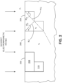
- Example embodiments provide a topology of diffractive elements to control the position of the focused nanojet beam and change the direction of nanojet beam orientation. Some embodiments use an optical element with the step-like geometry. In some embodiments, a step-like topology provides the combination of the nanojet beams, originating from the edges of the system, contributing to the formation of a final nanojet beam deflected from the normal direction. The cross-section and focusing function are schematically represented in FIG. 2 . The characteristics of the generated nanojet beams are controlled by the parameters of the corresponding parts of the step-like system, such as refractive index ratios between the dielectric materials forming the system, dimensions of the cavity, and angle of incidence of the illuminating wave.
- Some embodiments include a diffraction grating for diffracting light comprising a plurality of grating unit cells with step-like optical elements.
- the optical elements are positioned on a substrate surface.
- the step-like optical elements include step-like cavities or channels in a substrate filled by the dielectric material having higher refractive index.
- the second variant of diffraction grating represents the optical element protected from the mechanical damage and may have a simpler fabrication process.
- Example embodiments have been validated numerically via full-wave electromagnetic analysis of a 2D and 3D double-layer optical elements.
- the analysis assumed that all the materials are lossless and non-dispersive.
- the analysis has revealed that diffraction of a plane wave on an optical element based on the combination of different dielectric materials, can result in the deviation of the nanojet away from the normal direction in a case of normal incidence.
- the position of focal spot, angle of deviation, intensity and shape of nanojet beam can be controlled by the variation of the refractive indexes and sizes of the constitutive parts/blocks.
- the step-like diffraction grating achieves non-symmetrical distribution of an intensity leading to the high grating efficiency for the desired diffraction order.
- using elements with W ⁇ W ⁇ ⁇ the maximal input corresponds to the orders ⁇ 1.
- Some embodiments demonstrate very high diffraction uniformity (about 95%) for the first diffracted order.
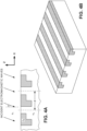
- FIG. 2 illustrates a cut-out portion of an optical component in which two grating elements 202 and 204 are shown inset into a substrate 206.
- Each grating element may be described as a stepped channel inset into the substrate.
- the grating elements have a refractive index n 2 , which in some embodiments is greater than the refractive index n 3 of the substrate.
- the ambient medium may have a refractive index of n 1 .
- Each grating element in this embodiment has two steps, with a first step 208 being arranged along (e.g. substantially coplanar with) the outer surface of the substrate and a second step 210 extending inward (downward, in FIG.
- the first and second steps may be contiguous with one another, with the dotted lines of FIG. 2 being shown only for the sake of clarity.
- the first step has a greater width than the second step.
- a side edge (the left side edge in FIG. 2 ) of the first step is aligned with the corresponding side edge of the second step.
- the cross-sectional view of FIG. 2 thus corresponds to a single material step-like element with refractive indexes n 2 embedded in a homogeneous dielectric media with a refractive index n 3 ( n 2 > n 3 ) .
- the full system is placed inside the homogeneous host medium with refractive index n 1 .
- n 1 can be equal to n 3 .
- the materials and size of the constitutive parts can be selected in order to manage the position of a nanojet hot spot and the intensity, direction and angle of deviation of a nanojet beam.
- some prismatic structures may also be used in some embodiments. Variation of the base angle value provides additional degree of freedom in the control of the nanojet beam radiation.
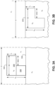
- FIG. 3A shows a diffraction grating with step-like elements, such as element 302 with refractive index n 2 , hosted by the homogeneous medium with refractive index n 1 and placed on a substrate surface 304 with refractive index n 3 ( n 2 , 3 > n 1 ) .
- n 2 > n 3 .
- Grating element 302 has a stepped structure with a first step 306 having a greater width than a second step 308.
- the second step 308 is positioned on the outer surface of the substrate 304, and the first step extends outward (upward, in FIG.
- FIG. 3A corresponds to the periodic array of step-like optical elements with refractive index n 2 embedded into the substrate with refractive index n 3 ( n 2 > n 3 > n 1 ) as illustrated in FIG. 2 .
- the grating constant or the period of the grating is d.
- a linearly polarized plane wave may be incident on the grating from the top in a plane perpendicular to the grating.
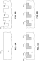
- FIGs. 4A-4B An embodiment of a grating with the second type of unit cell is presented in FIGs. 4A-4B .
- the step-like elements are made of a material having a refractive index greater than the refractive index of the substrate.
- materials that are used for the step-like elements include titanium dioxide (TiO 2 ) and silicon nitride (Si 3 N 4 ).
- FIGs. 6A-6D A method of making a diffraction grating according to some embodiments is illustrated in FIGs. 6A-6D .
- a substrate 600 is provided.
- Substrate 600 has first refractive index n 3 .
- Substrate 600 may be, for example, a waveguide for a waveguide display.
- a plurality of stepped channels are formed in an outer surface of the substrate 600, for example by chemical or mechanical etching.
- each of the stepped channels is filled with a material having a second refractive index n 2 greater than the first refractive index n 3 .
- polishing or other smoothing may be performed to provide a flush outer surface as shown in FIG. 6D .
- Such an outer surface may be more resistant to scratches and damage than a surface with protruding grating elements.
- additional protective or optical layers or coatings e.g. anti-reflective coatings
- Combinations of materials and dimensions of the elements of the grating for nanojet beam deflection may be selected according to equations and techniques described below.
- the total response of the diffraction grating is influenced by the phenomenon of edge diffraction into the single element of the period, as described in A. Boriskin, V. Drazic, R. Keating, M. Damghanian, O. Shramkova, L. Blondé, "Near field focusing by edge diffraction,” Opt. Lett., 2018 ("Boriskin et al.”).
- Data shown below was obtained using the COMSOL Multiphysics software.
- the presented analysis of the fields and power distributions inside the meta-elements of the gratings helps explain the physics of the phenomenon and allows for selection of topologies that provide desired properties.
- the beam-forming phenomenon is associated with the edge of the system, and the nanojet beam radiation angle is defined by Snell's law.
- ⁇ TIR sin ⁇ 1 n L n H is the critical angle of refraction.
- a combination of these two nanojets with the nanojet generated by the second step will increase the intensity of the final beam obtained at the bottom surface of the metalens.
- Below are example formulas for parameters of the elements that may be used get such a nanojet combination inside the element.
- the cross point (hot spot) of the two symmetrical nanojets NJ 1 and NJ 2 generated by the external edges of the large block on the top of the element may be used to select the approximate height of this block which can be estimated as: h 1 ⁇ W 2 tan ⁇ B .
- W is the full width of the larger step on the top, which may be chosen taking into account the full size of the system or width of the unit cell in a case of diffraction grating (W ⁇ d).
- the height of the second step may be selected to correspond to the value providing the desirable angle of deviation for the total nanojet generated outside the element. To prevent the additional reflection of the nanojets by the left external wall of the optical element, the heights are selected such that ( h 2 -h 1 ) ⁇ h 1 .
- the dimensions of the step-like elements may be selected to increase the diffraction uniformity for inclined incidence of electromagnetic wave. To do this, it may be considered that for the inclined incidence, the angles of deviation of NJ 1 and NJ 2 may not be equal, and, depending on the angle of incidence, there may be multiple nanojet reflections by the edges of the optical elements.
- a diffraction grating based on the step-like element may have the following performance characteristics.
- the simulations assume that a linearly polarized plane wave is incident on the grating from the top in a plane perpendicular to the grating.
- the angles of the diffracted beams are not influenced by the structure of the optical elements. Rather, they are determined by the period of the grating, wavelength of the incident plane wave and angle of wave incidence and can be calculated according to the grating equation.
- FIG. 4A is a cross sectional view of a portion of a diffraction grating configured according to FIG. 3B . Although three unit cells are illustrated in FIG. 4A , a diffraction grating according to some embodiments may include an array of tens, hundreds, or thousands of unit cells.
- FIG. 4B is a schematic cutaway perspective view of a portion of a diffraction grating as in FIG. 4A , illustrating four unit cells.
- the performance of the grating depends on the polarization of the incident wave and parameters (dimensions, form and material) of the elements. Unlike a diffraction grating containing symmetrical single-material optical elements (regular structure of the same spacing), example diffraction gratings based on the double-material elements achieves nonsymmetrical distribution of an intensity (T j ⁇ T -j , R j ⁇ R -j , where j is the diffraction order) leading to the maximal grating efficiency for the desired diffraction order. In the case of elements with W ⁇ ⁇ W ⁇ ⁇ the maximal input corresponds to the orders ⁇ 1.
- the full-wave electromagnetic analysis was done for the 2D array of double-material elements. The calculations assume that the system is infinite in X- and Y-directions.
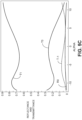
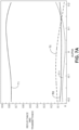
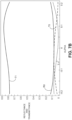
- FIGs. 5A-5C are graphs showing simulated results for reflectance and transmittance plotted against angle of electromagnetic wave incidence ⁇ .
- ⁇ 625nm
- d 494nm
- n 1 1.0
- n 3 1.5154.
- n 2 2.8
- W 300nm
- h 1 255nm
- h 2 475nm
- n 2 2.6
- W 300nm
- h 1 295nm
- h 2 500nm.
- h 1 420nm
- h 2 680nm.
- all the materials are lossless and non-dispersive.
- the presented simulations can be adapted to dispersive material without dramatic change of refractive index for three colors.
- the system demonstrates very high transmittivity.
- such a system of three waveguides may be used as the in-coupler for an augmented reality display without color correction.
- the high uniformity for all three colors avoids the dedication of the parts of the image signal to correct the brightness and color uniformity.
- Example embodiments include step-like microelements that deviate the focused beam in the near zone.
- the periodic array of step-like elements embedded into the dielectric substrate can be considered as the diffraction grating with nonsymmetrical distribution of an intensity and leading to high grating efficiency for the desired diffraction order.
- Some embodiments provide high diffraction uniformity (e.g. >95%) for the corresponding order.
- Some embodiments provide for relative ease of fabrication and robustness of the structure as a result of the flat surface of the diffraction grating. Fabrication may be performed, for example, by chemically or mechanically etching or otherwise forming a step-shaped channel in a substrate and filling the step-shaped channel with a material having a greater refractive index than the substrate.
- grating configuration for three wavelengths allows a system of three waveguides to be used as the in-coupler for an augmented reality display without color correction.
- Example embodiments maybe implemented in various optical systems that operate to deviate an image or some light with a micro-structure, with advantages including simplicity of fabrication and robustness.
- Example application domains are head-up displays, solar cell panels for maximizing light collection, OLED display light extraction, among many others.
- While the above examples refer primarily to the use of devices configured for visible light, other embodiments are configured for use with longer or shorter wavelengths, such as infrared or ultraviolet light, or for use with waves in other parts of the electromagnetic spectrum. Such embodiments may employ materials that are transparent to the wavelengths for which they are designed.
Landscapes
- Physics & Mathematics (AREA)
- General Physics & Mathematics (AREA)
- Optics & Photonics (AREA)
- Engineering & Computer Science (AREA)
- Manufacturing & Machinery (AREA)
- Diffracting Gratings Or Hologram Optical Elements (AREA)
Claims (12)
- Beugungsgitter, umfassend:ein Substrat (206, 600), das eine Außenfläche aufweist, wobei das Substrat einen ersten Brechungsindex aufweist;mehrere Gitterelemente (202, 204, 302, 602, 604, 606), wobei jedes Gitterelement einen in das Substrat eingelassenen gestuften Kanal umfasst, wobei der gestufte Kanal einen zweiten Brechungsindex aufweist, der größer als der erste Brechungsindex ist;wobei der gestufte Kanal ein zweistufiger Kanal ist, der eine erste Stufe (208, 306) entlang der Außenfläche des Substrats und eine zweite Stufe (210, 308), die sich von der ersten Stufe nach innen erstreckt, aufweist, wobei die erste Stufe eine größere Breite als die zweite Stufe aufweist;dadurch gekennzeichnet, dass die Höhe des gestuften Kanals weniger als das Zweifache der Höhe der ersten Stufe beträgt.
- Beugungsgitter nach Anspruch 1, wobei der gestufte Kanal eine Außenfläche aufweist, die im Wesentlichen koplanar mit der Außenfläche des Substrats verläuft.
- Beugungsgitter nach einem der Ansprüche 1 und 2, wobei die Breite der ersten Stufe (W) im Wesentlichen zweimal so groß wie die Breite der zweiten Stufe ist.
- Beugungsgitter nach einem der Ansprüche 1-3, wobei ein seitlicher Rand der ersten Stufe im Wesentlichen auf einen seitlichen Rand der zweiten Stufe ausgerichtet ist.
- Beugungsgitter nach einem der Ansprüche 1-4, wobei die erste Stufe eine Breite W und eine Höhe h1 aufweist, wobei


- Beugungsgitter nach einem der Ansprüche 1-5, wobei das Substrat ein Wellenleiter in einem Wellenleiter-Display ist.
- Verfahren zum Herstellen eines Beugungsgitters, umfassend:Bilden mehrerer gestufter Kanäle (202, 204, 302, 602, 604, 606) in einer Außenfläche eines Substrats (206, 600), das einen ersten Brechungsindex aufweist;wobei jeder gestufte Kanal ein zweistufiger Kanal ist, der eine erste Stufe (208, 306) entlang der Außenfläche des Substrats und eine zweite Stufe (210, 308), die sich von der ersten Stufe nach innen erstreckt, aufweist, wobei die erste Stufe eine größere Breite (W) als die zweite Stufe aufweist; undFüllen jedes der abgestuften Kanäle mit einem Material, das einen zweiten Brechungsindex aufweist, der größer als der erste Brechungsindex ist;dadurch gekennzeichnet, dass die Höhe (h2) jedes gestuften Kanals weniger als das Zweifache der Höhe (h1) der ersten Stufe beträgt.
- Verfahren nach Anspruch 7, wobei die Breite (W) der ersten Stufe im Wesentlichen zweimal so groß wie die Breite der zweiten Stufe ist.
- Verfahren nach einem der Ansprüche 7 und 8, wobei ein seitlicher Rand der ersten Stufe im Wesentlichen auf einen seitlichen Rand der zweiten Stufe ausgerichtet ist.
- Verfahren nach einem der Ansprüche 7-9, wobei die erste Stufe eine Breite W und eine Höhe h1 aufweist, wobei


- Verfahren nach einem der Ansprüche 7-10, wobei das Substrat ein Wellenleiter in einem Wellenleiter-Display ist.
- Optische Vorrichtung, umfassend:mindestens einen Wellenleiter (178, 180), der ein Substrat umfasst, das eine Außenfläche aufweist, wobei das Substrat einen ersten Brechungsindex aufweist, wobei der Wellenleiter einen Einkoppler (180, 184) aufweist;einen Bildgenerator (176), der dafür ausgelegt ist, Licht, das ein Bild darstellt, auf den Einkoppler zu richten;wobei der Einkoppler mehrere Gitterelemente (202, 204, 302, 602, 604, 606) umfasst, wobei jedes Gitterelement einen in das Substrat eingelassenen gestuften Kanal umfasst, wobei der gestufte Kanal einen zweiten Brechungsindex aufweist, der größer als der erste Brechungsindex ist, wobei der gestufte Kanal ein zweistufiger Kanal ist, der eine erste Stufe (208, 306) entlang der Außenfläche des Substrats und eine zweite Stufe (210, 308), die sich von der ersten Stufe nach innen erstreckt, aufweist, wobei die erste Stufe eine größere Breite als die zweite Stufe aufweist, wobei die erste Stufe eine größere Breite (W) als die zweite Stufe aufweist,dadurch gekennzeichnet, dass die Höhe des gestuften Kanals (h2) weniger als das Zweifache der Höhe (h1) der ersten Stufe beträgt.
Applications Claiming Priority (2)
| Application Number | Priority Date | Filing Date | Title |
|---|---|---|---|
| EP20305538 | 2020-05-22 | ||
| PCT/EP2021/063239 WO2021233968A1 (en) | 2020-05-22 | 2021-05-19 | High color uniformity double material diffraction grating comprising step-like cavities |
Publications (2)
| Publication Number | Publication Date |
|---|---|
| EP4154043A1 EP4154043A1 (de) | 2023-03-29 |
| EP4154043B1 true EP4154043B1 (de) | 2025-05-14 |
Family
ID=71465254
Family Applications (1)
| Application Number | Title | Priority Date | Filing Date |
|---|---|---|---|
| EP21727442.2A Active EP4154043B1 (de) | 2020-05-22 | 2021-05-19 | Doppelmaterialbeugungsgitter mit hoher farbuniformität und stufenförmigen hohlräumen |
Country Status (4)
| Country | Link |
|---|---|
| US (1) | US20230185004A1 (de) |
| EP (1) | EP4154043B1 (de) |
| CN (1) | CN115943329B (de) |
| WO (1) | WO2021233968A1 (de) |
Family Cites Families (14)
| Publication number | Priority date | Publication date | Assignee | Title |
|---|---|---|---|---|
| US5544268A (en) * | 1994-09-09 | 1996-08-06 | Deacon Research | Display panel with electrically-controlled waveguide-routing |
| JP3472097B2 (ja) * | 1997-08-20 | 2003-12-02 | キヤノン株式会社 | 回折光学素子及びそれを用いた光学系 |
| TWI266899B (en) * | 2002-02-12 | 2006-11-21 | Unaxis Balzers Ltd | Component comprising submicron hollow spaces |
| US7394535B1 (en) | 2007-03-20 | 2008-07-01 | Tokyo Electron Limited | Optical metrology using a photonic nanojet |
| US11320571B2 (en) * | 2012-11-16 | 2022-05-03 | Rockwell Collins, Inc. | Transparent waveguide display providing upper and lower fields of view with uniform light extraction |
| US8773599B2 (en) * | 2011-10-24 | 2014-07-08 | Google Inc. | Near-to-eye display with diffraction grating that bends and focuses light |
| US9557458B2 (en) * | 2013-10-29 | 2017-01-31 | CSEM Centre Suisse d'Electronique et de Microtechnique SA—Recherche et Développement | Optical grating coupling structure |
| US9513480B2 (en) | 2015-02-09 | 2016-12-06 | Microsoft Technology Licensing, Llc | Waveguide |
| US9791703B1 (en) | 2016-04-13 | 2017-10-17 | Microsoft Technology Licensing, Llc | Waveguides with extended field of view |
| WO2018039277A1 (en) * | 2016-08-22 | 2018-03-01 | Magic Leap, Inc. | Diffractive eyepiece |
| KR102629153B1 (ko) * | 2017-12-18 | 2024-01-24 | 엘지디스플레이 주식회사 | 광학식 이미지 인식 센서를 구비한 평판 표시장치 |
| FI128594B (en) * | 2017-12-22 | 2020-08-31 | Dispelix Oy | Stair waveguide elements, personal display device and method for producing an image |
| EP3540479A1 (de) | 2018-03-13 | 2019-09-18 | Thomson Licensing | Beugungsgitter mit doppelmaterialstrukturen |
| CN110764260A (zh) * | 2018-07-28 | 2020-02-07 | 华为技术有限公司 | 一种增强现实装置 |
-
2021
- 2021-05-19 EP EP21727442.2A patent/EP4154043B1/de active Active
- 2021-05-19 CN CN202180042532.XA patent/CN115943329B/zh active Active
- 2021-05-19 WO PCT/EP2021/063239 patent/WO2021233968A1/en not_active Ceased
- 2021-05-19 US US17/924,504 patent/US20230185004A1/en active Pending
Also Published As
| Publication number | Publication date |
|---|---|
| CN115943329A (zh) | 2023-04-07 |
| WO2021233968A1 (en) | 2021-11-25 |
| EP4154043A1 (de) | 2023-03-29 |
| CN115943329B (zh) | 2026-04-03 |
| US20230185004A1 (en) | 2023-06-15 |
Similar Documents
| Publication | Publication Date | Title |
|---|---|---|
| US11573356B2 (en) | Diffraction grating comprising double-materials structures | |
| EP4031927B1 (de) | Optische vorrichtung zum koppeln eines hohen blickfeldes von einfallendem licht | |
| US11275252B2 (en) | Device for forming at least one tilted focused beam in the near zone, from incident electromagnetic waves | |
| CN109073884B (zh) | 具有改进的强度分布的波导出射光瞳扩展器 | |
| US12228756B2 (en) | Optical device | |
| EP3223062A1 (de) | Vorrichtung zur bildung von mindestens einem fokussierten strahl im nahbereich aus einfallenden elektromagnetischen wellen | |
| US12174512B2 (en) | Device for forming an outgoing electromagnetic wave from an incident electromagnetic wave | |
| EP4127789B1 (de) | Unpolarisiertes lichtgitter in einem koppler | |
| US20250147319A1 (en) | Metasurface-based image combiner and augmented reality device employing same | |
| US20230400618A1 (en) | Single mode full color waveguide combiner using asymmetric transmissive and reflective diffraction gratings | |
| US12044860B2 (en) | Inhomogeneous microlens device for near-field focusing, beam forming, and high-efficiency far-field device implementation | |
| EP4154043B1 (de) | Doppelmaterialbeugungsgitter mit hoher farbuniformität und stufenförmigen hohlräumen | |
| WO2022008378A1 (en) | Reflective in-coupler design with high refractive index element using second diffraction order for near-eye displays | |
| US20240094537A1 (en) | Uniform incoupler for conical incidence | |
| WO2021233877A1 (en) | High-uniformity high refractive index material transmissive and reflective diffraction gratings | |
| Hong | Meta-form near eye visor |
Legal Events
| Date | Code | Title | Description |
|---|---|---|---|
| STAA | Information on the status of an ep patent application or granted ep patent |
Free format text: STATUS: UNKNOWN |
|
| STAA | Information on the status of an ep patent application or granted ep patent |
Free format text: STATUS: THE INTERNATIONAL PUBLICATION HAS BEEN MADE |
|
| PUAI | Public reference made under article 153(3) epc to a published international application that has entered the european phase |
Free format text: ORIGINAL CODE: 0009012 |
|
| STAA | Information on the status of an ep patent application or granted ep patent |
Free format text: STATUS: REQUEST FOR EXAMINATION WAS MADE |
|
| 17P | Request for examination filed |
Effective date: 20221117 |
|
| AK | Designated contracting states |
Kind code of ref document: A1 Designated state(s): AL AT BE BG CH CY CZ DE DK EE ES FI FR GB GR HR HU IE IS IT LI LT LU LV MC MK MT NL NO PL PT RO RS SE SI SK SM TR |
|
| DAV | Request for validation of the european patent (deleted) | ||
| DAX | Request for extension of the european patent (deleted) | ||
| GRAP | Despatch of communication of intention to grant a patent |
Free format text: ORIGINAL CODE: EPIDOSNIGR1 |
|
| STAA | Information on the status of an ep patent application or granted ep patent |
Free format text: STATUS: GRANT OF PATENT IS INTENDED |
|
| INTG | Intention to grant announced |
Effective date: 20241212 |
|
| GRAS | Grant fee paid |
Free format text: ORIGINAL CODE: EPIDOSNIGR3 |
|
| GRAA | (expected) grant |
Free format text: ORIGINAL CODE: 0009210 |
|
| STAA | Information on the status of an ep patent application or granted ep patent |
Free format text: STATUS: THE PATENT HAS BEEN GRANTED |
|
| P01 | Opt-out of the competence of the unified patent court (upc) registered |
Free format text: CASE NUMBER: APP_13081/2025 Effective date: 20250317 |
|
| AK | Designated contracting states |
Kind code of ref document: B1 Designated state(s): AL AT BE BG CH CY CZ DE DK EE ES FI FR GB GR HR HU IE IS IT LI LT LU LV MC MK MT NL NO PL PT RO RS SE SI SK SM TR |
|
| REG | Reference to a national code |
Ref country code: GB Ref legal event code: FG4D |
|
| REG | Reference to a national code |
Ref country code: CH Ref legal event code: EP |
|
| REG | Reference to a national code |
Ref country code: IE Ref legal event code: FG4D |
|
| REG | Reference to a national code |
Ref country code: DE Ref legal event code: R096 Ref document number: 602021030768 Country of ref document: DE |
|
| PGFP | Annual fee paid to national office [announced via postgrant information from national office to epo] |
Ref country code: DE Payment date: 20250528 Year of fee payment: 5 |
|
| PGFP | Annual fee paid to national office [announced via postgrant information from national office to epo] |
Ref country code: GB Payment date: 20250520 Year of fee payment: 5 |
|
| PGFP | Annual fee paid to national office [announced via postgrant information from national office to epo] |
Ref country code: FR Payment date: 20250526 Year of fee payment: 5 |
|
| PGFP | Annual fee paid to national office [announced via postgrant information from national office to epo] |
Ref country code: AT Payment date: 20250721 Year of fee payment: 5 |
|
| REG | Reference to a national code |
Ref country code: NL Ref legal event code: MP Effective date: 20250514 |
|
| PG25 | Lapsed in a contracting state [announced via postgrant information from national office to epo] |
Ref country code: PT Free format text: LAPSE BECAUSE OF FAILURE TO SUBMIT A TRANSLATION OF THE DESCRIPTION OR TO PAY THE FEE WITHIN THE PRESCRIBED TIME-LIMIT Effective date: 20250915 Ref country code: ES Free format text: LAPSE BECAUSE OF FAILURE TO SUBMIT A TRANSLATION OF THE DESCRIPTION OR TO PAY THE FEE WITHIN THE PRESCRIBED TIME-LIMIT Effective date: 20250514 Ref country code: FI Free format text: LAPSE BECAUSE OF FAILURE TO SUBMIT A TRANSLATION OF THE DESCRIPTION OR TO PAY THE FEE WITHIN THE PRESCRIBED TIME-LIMIT Effective date: 20250514 |
|
| REG | Reference to a national code |
Ref country code: LT Ref legal event code: MG9D |
|
| PG25 | Lapsed in a contracting state [announced via postgrant information from national office to epo] |
Ref country code: NO Free format text: LAPSE BECAUSE OF FAILURE TO SUBMIT A TRANSLATION OF THE DESCRIPTION OR TO PAY THE FEE WITHIN THE PRESCRIBED TIME-LIMIT Effective date: 20250814 Ref country code: GR Free format text: LAPSE BECAUSE OF FAILURE TO SUBMIT A TRANSLATION OF THE DESCRIPTION OR TO PAY THE FEE WITHIN THE PRESCRIBED TIME-LIMIT Effective date: 20250815 |
|
| PG25 | Lapsed in a contracting state [announced via postgrant information from national office to epo] |
Ref country code: PL Free format text: LAPSE BECAUSE OF FAILURE TO SUBMIT A TRANSLATION OF THE DESCRIPTION OR TO PAY THE FEE WITHIN THE PRESCRIBED TIME-LIMIT Effective date: 20250514 Ref country code: NL Free format text: LAPSE BECAUSE OF FAILURE TO SUBMIT A TRANSLATION OF THE DESCRIPTION OR TO PAY THE FEE WITHIN THE PRESCRIBED TIME-LIMIT Effective date: 20250514 |
|
| REG | Reference to a national code |
Ref country code: AT Ref legal event code: MK05 Ref document number: 1795244 Country of ref document: AT Kind code of ref document: T Effective date: 20250514 |
|
| PG25 | Lapsed in a contracting state [announced via postgrant information from national office to epo] |
Ref country code: BG Free format text: LAPSE BECAUSE OF FAILURE TO SUBMIT A TRANSLATION OF THE DESCRIPTION OR TO PAY THE FEE WITHIN THE PRESCRIBED TIME-LIMIT Effective date: 20250514 |
|
| PG25 | Lapsed in a contracting state [announced via postgrant information from national office to epo] |
Ref country code: HR Free format text: LAPSE BECAUSE OF FAILURE TO SUBMIT A TRANSLATION OF THE DESCRIPTION OR TO PAY THE FEE WITHIN THE PRESCRIBED TIME-LIMIT Effective date: 20250514 |
|
| PG25 | Lapsed in a contracting state [announced via postgrant information from national office to epo] |
Ref country code: AT Free format text: LAPSE BECAUSE OF FAILURE TO SUBMIT A TRANSLATION OF THE DESCRIPTION OR TO PAY THE FEE WITHIN THE PRESCRIBED TIME-LIMIT Effective date: 20250514 |
|
| PG25 | Lapsed in a contracting state [announced via postgrant information from national office to epo] |
Ref country code: RS Free format text: LAPSE BECAUSE OF FAILURE TO SUBMIT A TRANSLATION OF THE DESCRIPTION OR TO PAY THE FEE WITHIN THE PRESCRIBED TIME-LIMIT Effective date: 20250814 |
|
| PG25 | Lapsed in a contracting state [announced via postgrant information from national office to epo] |
Ref country code: IS Free format text: LAPSE BECAUSE OF FAILURE TO SUBMIT A TRANSLATION OF THE DESCRIPTION OR TO PAY THE FEE WITHIN THE PRESCRIBED TIME-LIMIT Effective date: 20250914 |
|
| PG25 | Lapsed in a contracting state [announced via postgrant information from national office to epo] |
Ref country code: LV Free format text: LAPSE BECAUSE OF FAILURE TO SUBMIT A TRANSLATION OF THE DESCRIPTION OR TO PAY THE FEE WITHIN THE PRESCRIBED TIME-LIMIT Effective date: 20250514 |
|
| REG | Reference to a national code |
Ref country code: CH Ref legal event code: H13 Free format text: ST27 STATUS EVENT CODE: U-0-0-H10-H13 (AS PROVIDED BY THE NATIONAL OFFICE) Effective date: 20251223 |
|
| PG25 | Lapsed in a contracting state [announced via postgrant information from national office to epo] |
Ref country code: DK Free format text: LAPSE BECAUSE OF FAILURE TO SUBMIT A TRANSLATION OF THE DESCRIPTION OR TO PAY THE FEE WITHIN THE PRESCRIBED TIME-LIMIT Effective date: 20250514 Ref country code: SM Free format text: LAPSE BECAUSE OF FAILURE TO SUBMIT A TRANSLATION OF THE DESCRIPTION OR TO PAY THE FEE WITHIN THE PRESCRIBED TIME-LIMIT Effective date: 20250514 |
|
| PG25 | Lapsed in a contracting state [announced via postgrant information from national office to epo] |
Ref country code: LU Free format text: LAPSE BECAUSE OF NON-PAYMENT OF DUE FEES Effective date: 20250519 |
|
| PG25 | Lapsed in a contracting state [announced via postgrant information from national office to epo] |
Ref country code: CH Free format text: LAPSE BECAUSE OF NON-PAYMENT OF DUE FEES Effective date: 20250531 |
|
| PG25 | Lapsed in a contracting state [announced via postgrant information from national office to epo] |
Ref country code: CZ Free format text: LAPSE BECAUSE OF FAILURE TO SUBMIT A TRANSLATION OF THE DESCRIPTION OR TO PAY THE FEE WITHIN THE PRESCRIBED TIME-LIMIT Effective date: 20250514 |
|
| PG25 | Lapsed in a contracting state [announced via postgrant information from national office to epo] |
Ref country code: EE Free format text: LAPSE BECAUSE OF FAILURE TO SUBMIT A TRANSLATION OF THE DESCRIPTION OR TO PAY THE FEE WITHIN THE PRESCRIBED TIME-LIMIT Effective date: 20250514 |
|
| PG25 | Lapsed in a contracting state [announced via postgrant information from national office to epo] |
Ref country code: SK Free format text: LAPSE BECAUSE OF FAILURE TO SUBMIT A TRANSLATION OF THE DESCRIPTION OR TO PAY THE FEE WITHIN THE PRESCRIBED TIME-LIMIT Effective date: 20250514 |
|
| PG25 | Lapsed in a contracting state [announced via postgrant information from national office to epo] |
Ref country code: IT Free format text: LAPSE BECAUSE OF FAILURE TO SUBMIT A TRANSLATION OF THE DESCRIPTION OR TO PAY THE FEE WITHIN THE PRESCRIBED TIME-LIMIT Effective date: 20250514 |
|
| REG | Reference to a national code |
Ref country code: BE Ref legal event code: MM Effective date: 20250531 |
|
| PG25 | Lapsed in a contracting state [announced via postgrant information from national office to epo] |
Ref country code: RO Free format text: LAPSE BECAUSE OF FAILURE TO SUBMIT A TRANSLATION OF THE DESCRIPTION OR TO PAY THE FEE WITHIN THE PRESCRIBED TIME-LIMIT Effective date: 20250514 |
|
| REG | Reference to a national code |
Ref country code: DE Ref legal event code: R097 Ref document number: 602021030768 Country of ref document: DE |
|
| PG25 | Lapsed in a contracting state [announced via postgrant information from national office to epo] |
Ref country code: MC Free format text: LAPSE BECAUSE OF FAILURE TO SUBMIT A TRANSLATION OF THE DESCRIPTION OR TO PAY THE FEE WITHIN THE PRESCRIBED TIME-LIMIT Effective date: 20250514 |
|
| PLBE | No opposition filed within time limit |
Free format text: ORIGINAL CODE: 0009261 |
|
| STAA | Information on the status of an ep patent application or granted ep patent |
Free format text: STATUS: NO OPPOSITION FILED WITHIN TIME LIMIT |
|
| REG | Reference to a national code |
Ref country code: CH Ref legal event code: L10 Free format text: ST27 STATUS EVENT CODE: U-0-0-L10-L00 (AS PROVIDED BY THE NATIONAL OFFICE) Effective date: 20260325 |
|
| PG25 | Lapsed in a contracting state [announced via postgrant information from national office to epo] |
Ref country code: IE Free format text: LAPSE BECAUSE OF NON-PAYMENT OF DUE FEES Effective date: 20250519 |
|
| PG25 | Lapsed in a contracting state [announced via postgrant information from national office to epo] |
Ref country code: BE Free format text: LAPSE BECAUSE OF NON-PAYMENT OF DUE FEES Effective date: 20250531 |
|
| 26N | No opposition filed |
Effective date: 20260217 |