EP4121299B1 - Élément de sécurité plat présentant des caractéristiques de sécurité optique - Google Patents
Élément de sécurité plat présentant des caractéristiques de sécurité optique Download PDFInfo
- Publication number
- EP4121299B1 EP4121299B1 EP21712759.6A EP21712759A EP4121299B1 EP 4121299 B1 EP4121299 B1 EP 4121299B1 EP 21712759 A EP21712759 A EP 21712759A EP 4121299 B1 EP4121299 B1 EP 4121299B1
- Authority
- EP
- European Patent Office
- Prior art keywords
- sub
- surface region
- security element
- wavelength structure
- wavelength
- Prior art date
- Legal status (The legal status is an assumption and is not a legal conclusion. Google has not performed a legal analysis and makes no representation as to the accuracy of the status listed.)
- Active
Links
- 230000003287 optical effect Effects 0.000 title claims description 7
- 238000000576 coating method Methods 0.000 claims description 99
- 239000011248 coating agent Substances 0.000 claims description 90
- 230000000694 effects Effects 0.000 claims description 24
- 238000013500 data storage Methods 0.000 claims 1
- 239000010410 layer Substances 0.000 description 97
- 239000006096 absorbing agent Substances 0.000 description 17
- 229910052751 metal Inorganic materials 0.000 description 14
- 239000002184 metal Substances 0.000 description 14
- PXHVJJICTQNCMI-UHFFFAOYSA-N Nickel Chemical compound [Ni] PXHVJJICTQNCMI-UHFFFAOYSA-N 0.000 description 10
- 239000000758 substrate Substances 0.000 description 9
- 239000003086 colorant Substances 0.000 description 8
- 239000004922 lacquer Substances 0.000 description 8
- -1 sodium aluminum fluorides Chemical class 0.000 description 8
- 229910052802 copper Inorganic materials 0.000 description 6
- 239000010949 copper Substances 0.000 description 6
- 238000000034 method Methods 0.000 description 6
- 230000000737 periodic effect Effects 0.000 description 6
- 239000010409 thin film Substances 0.000 description 6
- RYGMFSIKBFXOCR-UHFFFAOYSA-N Copper Chemical compound [Cu] RYGMFSIKBFXOCR-UHFFFAOYSA-N 0.000 description 5
- KDLHZDBZIXYQEI-UHFFFAOYSA-N Palladium Chemical compound [Pd] KDLHZDBZIXYQEI-UHFFFAOYSA-N 0.000 description 5
- 229910052782 aluminium Inorganic materials 0.000 description 5
- SZVJSHCCFOBDDC-UHFFFAOYSA-N ferrosoferric oxide Chemical compound O=[Fe]O[Fe]O[Fe]=O SZVJSHCCFOBDDC-UHFFFAOYSA-N 0.000 description 5
- 239000010408 film Substances 0.000 description 5
- 229910052759 nickel Inorganic materials 0.000 description 5
- 239000000049 pigment Substances 0.000 description 5
- BASFCYQUMIYNBI-UHFFFAOYSA-N platinum Chemical compound [Pt] BASFCYQUMIYNBI-UHFFFAOYSA-N 0.000 description 5
- VYZAMTAEIAYCRO-UHFFFAOYSA-N Chromium Chemical compound [Cr] VYZAMTAEIAYCRO-UHFFFAOYSA-N 0.000 description 4
- XEEYBQQBJWHFJM-UHFFFAOYSA-N Iron Chemical compound [Fe] XEEYBQQBJWHFJM-UHFFFAOYSA-N 0.000 description 4
- XAGFODPZIPBFFR-UHFFFAOYSA-N aluminium Chemical compound [Al] XAGFODPZIPBFFR-UHFFFAOYSA-N 0.000 description 4
- 229910052804 chromium Inorganic materials 0.000 description 4
- 239000011651 chromium Substances 0.000 description 4
- 229920001577 copolymer Polymers 0.000 description 4
- 229910052737 gold Inorganic materials 0.000 description 4
- 239000010931 gold Substances 0.000 description 4
- 239000000463 material Substances 0.000 description 4
- 239000004952 Polyamide Substances 0.000 description 3
- VYPSYNLAJGMNEJ-UHFFFAOYSA-N Silicium dioxide Chemical compound O=[Si]=O VYPSYNLAJGMNEJ-UHFFFAOYSA-N 0.000 description 3
- XLOMVQKBTHCTTD-UHFFFAOYSA-N Zinc monoxide Chemical compound [Zn]=O XLOMVQKBTHCTTD-UHFFFAOYSA-N 0.000 description 3
- 229910045601 alloy Inorganic materials 0.000 description 3
- 239000000956 alloy Substances 0.000 description 3
- ADCOVFLJGNWWNZ-UHFFFAOYSA-N antimony trioxide Chemical compound O=[Sb]O[Sb]=O ADCOVFLJGNWWNZ-UHFFFAOYSA-N 0.000 description 3
- 230000001427 coherent effect Effects 0.000 description 3
- PCHJSUWPFVWCPO-UHFFFAOYSA-N gold Chemical compound [Au] PCHJSUWPFVWCPO-UHFFFAOYSA-N 0.000 description 3
- PJXISJQVUVHSOJ-UHFFFAOYSA-N indium(iii) oxide Chemical compound [O-2].[O-2].[O-2].[In+3].[In+3] PJXISJQVUVHSOJ-UHFFFAOYSA-N 0.000 description 3
- UQSXHKLRYXJYBZ-UHFFFAOYSA-N iron oxide Inorganic materials [Fe]=O UQSXHKLRYXJYBZ-UHFFFAOYSA-N 0.000 description 3
- 239000000178 monomer Substances 0.000 description 3
- 229910052763 palladium Inorganic materials 0.000 description 3
- 229910052697 platinum Inorganic materials 0.000 description 3
- 229920002647 polyamide Polymers 0.000 description 3
- 229910052709 silver Inorganic materials 0.000 description 3
- 239000011135 tin Substances 0.000 description 3
- 229910052718 tin Inorganic materials 0.000 description 3
- ZNOKGRXACCSDPY-UHFFFAOYSA-N tungsten trioxide Chemical compound O=[W](=O)=O ZNOKGRXACCSDPY-UHFFFAOYSA-N 0.000 description 3
- VFLXBUJKRRJAKY-UHFFFAOYSA-N 13768-86-0 Chemical compound O=[Se](=O)=O VFLXBUJKRRJAKY-UHFFFAOYSA-N 0.000 description 2
- OKTJSMMVPCPJKN-UHFFFAOYSA-N Carbon Chemical compound [C] OKTJSMMVPCPJKN-UHFFFAOYSA-N 0.000 description 2
- 239000004986 Cholesteric liquid crystals (ChLC) Substances 0.000 description 2
- 229920000106 Liquid crystal polymer Polymers 0.000 description 2
- 239000002033 PVDF binder Substances 0.000 description 2
- 229930040373 Paraformaldehyde Natural products 0.000 description 2
- 239000004696 Poly ether ether ketone Substances 0.000 description 2
- 239000004698 Polyethylene Substances 0.000 description 2
- 239000004642 Polyimide Substances 0.000 description 2
- 239000004734 Polyphenylene sulfide Substances 0.000 description 2
- 239000004743 Polypropylene Substances 0.000 description 2
- 229910052581 Si3N4 Inorganic materials 0.000 description 2
- BQCADISMDOOEFD-UHFFFAOYSA-N Silver Chemical compound [Ag] BQCADISMDOOEFD-UHFFFAOYSA-N 0.000 description 2
- ATJFFYVFTNAWJD-UHFFFAOYSA-N Tin Chemical compound [Sn] ATJFFYVFTNAWJD-UHFFFAOYSA-N 0.000 description 2
- GWEVSGVZZGPLCZ-UHFFFAOYSA-N Titan oxide Chemical compound O=[Ti]=O GWEVSGVZZGPLCZ-UHFFFAOYSA-N 0.000 description 2
- 239000012790 adhesive layer Substances 0.000 description 2
- 229910052799 carbon Inorganic materials 0.000 description 2
- 229910000420 cerium oxide Inorganic materials 0.000 description 2
- 239000003989 dielectric material Substances 0.000 description 2
- 229920000840 ethylene tetrafluoroethylene copolymer Polymers 0.000 description 2
- 229910001940 europium oxide Inorganic materials 0.000 description 2
- AEBZCFFCDTZXHP-UHFFFAOYSA-N europium(3+);oxygen(2-) Chemical compound [O-2].[O-2].[O-2].[Eu+3].[Eu+3] AEBZCFFCDTZXHP-UHFFFAOYSA-N 0.000 description 2
- 230000005284 excitation Effects 0.000 description 2
- JEIPFZHSYJVQDO-UHFFFAOYSA-N ferric oxide Chemical compound O=[Fe]O[Fe]=O JEIPFZHSYJVQDO-UHFFFAOYSA-N 0.000 description 2
- 229910003437 indium oxide Inorganic materials 0.000 description 2
- AMGQUBHHOARCQH-UHFFFAOYSA-N indium;oxotin Chemical compound [In].[Sn]=O AMGQUBHHOARCQH-UHFFFAOYSA-N 0.000 description 2
- AXZKOIWUVFPNLO-UHFFFAOYSA-N magnesium;oxygen(2-) Chemical compound [O-2].[Mg+2] AXZKOIWUVFPNLO-UHFFFAOYSA-N 0.000 description 2
- 238000004519 manufacturing process Methods 0.000 description 2
- 229920000620 organic polymer Polymers 0.000 description 2
- BMMGVYCKOGBVEV-UHFFFAOYSA-N oxo(oxoceriooxy)cerium Chemical compound [Ce]=O.O=[Ce]=O BMMGVYCKOGBVEV-UHFFFAOYSA-N 0.000 description 2
- SIWVEOZUMHYXCS-UHFFFAOYSA-N oxo(oxoyttriooxy)yttrium Chemical compound O=[Y]O[Y]=O SIWVEOZUMHYXCS-UHFFFAOYSA-N 0.000 description 2
- BPUBBGLMJRNUCC-UHFFFAOYSA-N oxygen(2-);tantalum(5+) Chemical compound [O-2].[O-2].[O-2].[O-2].[O-2].[Ta+5].[Ta+5] BPUBBGLMJRNUCC-UHFFFAOYSA-N 0.000 description 2
- 229920002492 poly(sulfone) Polymers 0.000 description 2
- 229920006260 polyaryletherketone Polymers 0.000 description 2
- 229920001707 polybutylene terephthalate Polymers 0.000 description 2
- 229920002530 polyetherether ketone Polymers 0.000 description 2
- 229920000573 polyethylene Polymers 0.000 description 2
- 229920000139 polyethylene terephthalate Polymers 0.000 description 2
- 239000005020 polyethylene terephthalate Substances 0.000 description 2
- 229920001721 polyimide Polymers 0.000 description 2
- 229920006324 polyoxymethylene Polymers 0.000 description 2
- 229920000069 polyphenylene sulfide Polymers 0.000 description 2
- 229920001155 polypropylene Polymers 0.000 description 2
- 229920001343 polytetrafluoroethylene Polymers 0.000 description 2
- 239000004810 polytetrafluoroethylene Substances 0.000 description 2
- 239000004800 polyvinyl chloride Substances 0.000 description 2
- 229920002620 polyvinyl fluoride Polymers 0.000 description 2
- 229920002981 polyvinylidene fluoride Polymers 0.000 description 2
- 229910003447 praseodymium oxide Inorganic materials 0.000 description 2
- FKTOIHSPIPYAPE-UHFFFAOYSA-N samarium(iii) oxide Chemical compound [O-2].[O-2].[O-2].[Sm+3].[Sm+3] FKTOIHSPIPYAPE-UHFFFAOYSA-N 0.000 description 2
- LIVNPJMFVYWSIS-UHFFFAOYSA-N silicon monoxide Chemical compound [Si-]#[O+] LIVNPJMFVYWSIS-UHFFFAOYSA-N 0.000 description 2
- HQVNEWCFYHHQES-UHFFFAOYSA-N silicon nitride Chemical compound N12[Si]34N5[Si]62N3[Si]51N64 HQVNEWCFYHHQES-UHFFFAOYSA-N 0.000 description 2
- 239000004332 silver Substances 0.000 description 2
- 239000011734 sodium Substances 0.000 description 2
- 125000006850 spacer group Chemical group 0.000 description 2
- 238000004544 sputter deposition Methods 0.000 description 2
- PBCFLUZVCVVTBY-UHFFFAOYSA-N tantalum pentoxide Inorganic materials O=[Ta](=O)O[Ta](=O)=O PBCFLUZVCVVTBY-UHFFFAOYSA-N 0.000 description 2
- XOLBLPGZBRYERU-UHFFFAOYSA-N tin dioxide Chemical compound O=[Sn]=O XOLBLPGZBRYERU-UHFFFAOYSA-N 0.000 description 2
- 238000007740 vapor deposition Methods 0.000 description 2
- 229910018072 Al 2 O 3 Inorganic materials 0.000 description 1
- KLZUFWVZNOTSEM-UHFFFAOYSA-K Aluminium flouride Chemical compound F[Al](F)F KLZUFWVZNOTSEM-UHFFFAOYSA-K 0.000 description 1
- 229910016036 BaF 2 Inorganic materials 0.000 description 1
- 229910021193 La 2 O 3 Inorganic materials 0.000 description 1
- ZOKXTWBITQBERF-UHFFFAOYSA-N Molybdenum Chemical compound [Mo] ZOKXTWBITQBERF-UHFFFAOYSA-N 0.000 description 1
- 229910017493 Nd 2 O 3 Inorganic materials 0.000 description 1
- 239000000020 Nitrocellulose Substances 0.000 description 1
- 229920008285 Poly(ether ketone) PEK Polymers 0.000 description 1
- 229910004298 SiO 2 Inorganic materials 0.000 description 1
- 229910006404 SnO 2 Inorganic materials 0.000 description 1
- 229910010413 TiO 2 Inorganic materials 0.000 description 1
- RTAQQCXQSZGOHL-UHFFFAOYSA-N Titanium Chemical compound [Ti] RTAQQCXQSZGOHL-UHFFFAOYSA-N 0.000 description 1
- 239000005083 Zinc sulfide Substances 0.000 description 1
- 238000010521 absorption reaction Methods 0.000 description 1
- 150000001252 acrylic acid derivatives Chemical class 0.000 description 1
- 239000004676 acrylonitrile butadiene styrene Substances 0.000 description 1
- 239000000853 adhesive Substances 0.000 description 1
- 239000004411 aluminium Substances 0.000 description 1
- OYLGJCQECKOTOL-UHFFFAOYSA-L barium fluoride Chemical compound [F-].[F-].[Ba+2] OYLGJCQECKOTOL-UHFFFAOYSA-L 0.000 description 1
- 229910001632 barium fluoride Inorganic materials 0.000 description 1
- 239000011127 biaxially oriented polypropylene Substances 0.000 description 1
- 230000005540 biological transmission Effects 0.000 description 1
- WUKWITHWXAAZEY-UHFFFAOYSA-L calcium difluoride Chemical compound [F-].[F-].[Ca+2] WUKWITHWXAAZEY-UHFFFAOYSA-L 0.000 description 1
- QCCDYNYSHILRDG-UHFFFAOYSA-K cerium(3+);trifluoride Chemical compound [F-].[F-].[F-].[Ce+3] QCCDYNYSHILRDG-UHFFFAOYSA-K 0.000 description 1
- 229910017052 cobalt Inorganic materials 0.000 description 1
- 239000010941 cobalt Substances 0.000 description 1
- GUTLYIVDDKVIGB-UHFFFAOYSA-N cobalt atom Chemical compound [Co] GUTLYIVDDKVIGB-UHFFFAOYSA-N 0.000 description 1
- 238000004040 coloring Methods 0.000 description 1
- 238000004132 cross linking Methods 0.000 description 1
- 230000001186 cumulative effect Effects 0.000 description 1
- 238000007766 curtain coating Methods 0.000 description 1
- 238000000151 deposition Methods 0.000 description 1
- 230000008021 deposition Effects 0.000 description 1
- 238000003618 dip coating Methods 0.000 description 1
- 238000004049 embossing Methods 0.000 description 1
- QHSJIZLJUFMIFP-UHFFFAOYSA-N ethene;1,1,2,2-tetrafluoroethene Chemical group C=C.FC(F)=C(F)F QHSJIZLJUFMIFP-UHFFFAOYSA-N 0.000 description 1
- ZIFQMRCKKMHKAN-UHFFFAOYSA-N ethene;1,1,2,3,3,3-hexafluoroprop-1-ene;1,1,2,2-tetrafluoroethene Chemical group C=C.FC(F)=C(F)F.FC(F)=C(F)C(F)(F)F ZIFQMRCKKMHKAN-UHFFFAOYSA-N 0.000 description 1
- 229920002457 flexible plastic Polymers 0.000 description 1
- 229910052735 hafnium Inorganic materials 0.000 description 1
- WIHZLLGSGQNAGK-UHFFFAOYSA-N hafnium(4+);oxygen(2-) Chemical compound [O-2].[O-2].[Hf+4] WIHZLLGSGQNAGK-UHFFFAOYSA-N 0.000 description 1
- CJNBYAVZURUTKZ-UHFFFAOYSA-N hafnium(iv) oxide Chemical compound O=[Hf]=O CJNBYAVZURUTKZ-UHFFFAOYSA-N 0.000 description 1
- WHJFNYXPKGDKBB-UHFFFAOYSA-N hafnium;methane Chemical compound C.[Hf] WHJFNYXPKGDKBB-UHFFFAOYSA-N 0.000 description 1
- 238000005286 illumination Methods 0.000 description 1
- 229910052738 indium Inorganic materials 0.000 description 1
- 229910052742 iron Inorganic materials 0.000 description 1
- 235000013980 iron oxide Nutrition 0.000 description 1
- VBMVTYDPPZVILR-UHFFFAOYSA-N iron(2+);oxygen(2-) Chemical class [O-2].[Fe+2] VBMVTYDPPZVILR-UHFFFAOYSA-N 0.000 description 1
- 238000003475 lamination Methods 0.000 description 1
- MRELNEQAGSRDBK-UHFFFAOYSA-N lanthanum(3+);oxygen(2-) Chemical compound [O-2].[O-2].[O-2].[La+3].[La+3] MRELNEQAGSRDBK-UHFFFAOYSA-N 0.000 description 1
- 239000007788 liquid Substances 0.000 description 1
- PQXKHYXIUOZZFA-UHFFFAOYSA-M lithium fluoride Chemical compound [Li+].[F-] PQXKHYXIUOZZFA-UHFFFAOYSA-M 0.000 description 1
- ORUIBWPALBXDOA-UHFFFAOYSA-L magnesium fluoride Chemical compound [F-].[F-].[Mg+2] ORUIBWPALBXDOA-UHFFFAOYSA-L 0.000 description 1
- 239000000395 magnesium oxide Substances 0.000 description 1
- CPLXHLVBOLITMK-UHFFFAOYSA-N magnesium oxide Inorganic materials [Mg]=O CPLXHLVBOLITMK-UHFFFAOYSA-N 0.000 description 1
- 229910001512 metal fluoride Inorganic materials 0.000 description 1
- 238000001465 metallisation Methods 0.000 description 1
- 229910052750 molybdenum Inorganic materials 0.000 description 1
- 239000011733 molybdenum Substances 0.000 description 1
- 239000002086 nanomaterial Substances 0.000 description 1
- PLDDOISOJJCEMH-UHFFFAOYSA-N neodymium(3+);oxygen(2-) Chemical compound [O-2].[O-2].[O-2].[Nd+3].[Nd+3] PLDDOISOJJCEMH-UHFFFAOYSA-N 0.000 description 1
- 229910052758 niobium Inorganic materials 0.000 description 1
- 239000010955 niobium Substances 0.000 description 1
- GUCVJGMIXFAOAE-UHFFFAOYSA-N niobium atom Chemical compound [Nb] GUCVJGMIXFAOAE-UHFFFAOYSA-N 0.000 description 1
- 229920001220 nitrocellulos Polymers 0.000 description 1
- 239000005026 oriented polypropylene Substances 0.000 description 1
- TWNQGVIAIRXVLR-UHFFFAOYSA-N oxo(oxoalumanyloxy)alumane Chemical compound O=[Al]O[Al]=O TWNQGVIAIRXVLR-UHFFFAOYSA-N 0.000 description 1
- NDLPOXTZKUMGOV-UHFFFAOYSA-N oxo(oxoferriooxy)iron hydrate Chemical compound O.O=[Fe]O[Fe]=O NDLPOXTZKUMGOV-UHFFFAOYSA-N 0.000 description 1
- MMKQUGHLEMYQSG-UHFFFAOYSA-N oxygen(2-);praseodymium(3+) Chemical compound [O-2].[O-2].[O-2].[Pr+3].[Pr+3] MMKQUGHLEMYQSG-UHFFFAOYSA-N 0.000 description 1
- RUDFQVOCFDJEEF-UHFFFAOYSA-N oxygen(2-);yttrium(3+) Chemical compound [O-2].[O-2].[O-2].[Y+3].[Y+3] RUDFQVOCFDJEEF-UHFFFAOYSA-N 0.000 description 1
- 238000010422 painting Methods 0.000 description 1
- 229920003023 plastic Polymers 0.000 description 1
- 239000004033 plastic Substances 0.000 description 1
- 239000002985 plastic film Substances 0.000 description 1
- 229920000515 polycarbonate Polymers 0.000 description 1
- 239000004417 polycarbonate Substances 0.000 description 1
- 229920000728 polyester Polymers 0.000 description 1
- 239000011112 polyethylene naphthalate Substances 0.000 description 1
- 229920000642 polymer Polymers 0.000 description 1
- 229920000915 polyvinyl chloride Polymers 0.000 description 1
- 230000001681 protective effect Effects 0.000 description 1
- OJIKOZJGHCVMDC-UHFFFAOYSA-K samarium(iii) fluoride Chemical compound F[Sm](F)F OJIKOZJGHCVMDC-UHFFFAOYSA-K 0.000 description 1
- 239000011669 selenium Substances 0.000 description 1
- 239000004065 semiconductor Substances 0.000 description 1
- 238000000926 separation method Methods 0.000 description 1
- 229910052710 silicon Inorganic materials 0.000 description 1
- 239000010703 silicon Substances 0.000 description 1
- HBMJWWWQQXIZIP-UHFFFAOYSA-N silicon carbide Chemical compound [Si+]#[C-] HBMJWWWQQXIZIP-UHFFFAOYSA-N 0.000 description 1
- 239000000377 silicon dioxide Substances 0.000 description 1
- 235000012239 silicon dioxide Nutrition 0.000 description 1
- 229910052814 silicon oxide Inorganic materials 0.000 description 1
- 239000010944 silver (metal) Substances 0.000 description 1
- 230000003595 spectral effect Effects 0.000 description 1
- 238000005507 spraying Methods 0.000 description 1
- 239000000126 substance Substances 0.000 description 1
- 238000004381 surface treatment Methods 0.000 description 1
- 229910052715 tantalum Inorganic materials 0.000 description 1
- GUVRBAGPIYLISA-UHFFFAOYSA-N tantalum atom Chemical compound [Ta] GUVRBAGPIYLISA-UHFFFAOYSA-N 0.000 description 1
- YEAUATLBSVJFOY-UHFFFAOYSA-N tetraantimony hexaoxide Chemical compound O1[Sb](O2)O[Sb]3O[Sb]1O[Sb]2O3 YEAUATLBSVJFOY-UHFFFAOYSA-N 0.000 description 1
- 229910001887 tin oxide Inorganic materials 0.000 description 1
- 239000010936 titanium Substances 0.000 description 1
- 229910052719 titanium Inorganic materials 0.000 description 1
- BYMUNNMMXKDFEZ-UHFFFAOYSA-K trifluorolanthanum Chemical compound F[La](F)F BYMUNNMMXKDFEZ-UHFFFAOYSA-K 0.000 description 1
- XRADHEAKQRNYQQ-UHFFFAOYSA-K trifluoroneodymium Chemical compound F[Nd](F)F XRADHEAKQRNYQQ-UHFFFAOYSA-K 0.000 description 1
- WFKWXMTUELFFGS-UHFFFAOYSA-N tungsten Chemical compound [W] WFKWXMTUELFFGS-UHFFFAOYSA-N 0.000 description 1
- 229910052721 tungsten Inorganic materials 0.000 description 1
- 239000010937 tungsten Substances 0.000 description 1
- 229910052720 vanadium Inorganic materials 0.000 description 1
- LEONUFNNVUYDNQ-UHFFFAOYSA-N vanadium atom Chemical compound [V] LEONUFNNVUYDNQ-UHFFFAOYSA-N 0.000 description 1
- 229910052984 zinc sulfide Inorganic materials 0.000 description 1
- DRDVZXDWVBGGMH-UHFFFAOYSA-N zinc;sulfide Chemical compound [S-2].[Zn+2] DRDVZXDWVBGGMH-UHFFFAOYSA-N 0.000 description 1
Images
Classifications
-
- B—PERFORMING OPERATIONS; TRANSPORTING
- B42—BOOKBINDING; ALBUMS; FILES; SPECIAL PRINTED MATTER
- B42D—BOOKS; BOOK COVERS; LOOSE LEAVES; PRINTED MATTER CHARACTERISED BY IDENTIFICATION OR SECURITY FEATURES; PRINTED MATTER OF SPECIAL FORMAT OR STYLE NOT OTHERWISE PROVIDED FOR; DEVICES FOR USE THEREWITH AND NOT OTHERWISE PROVIDED FOR; MOVABLE-STRIP WRITING OR READING APPARATUS
- B42D25/00—Information-bearing cards or sheet-like structures characterised by identification or security features; Manufacture thereof
- B42D25/30—Identification or security features, e.g. for preventing forgery
- B42D25/324—Reliefs
-
- B—PERFORMING OPERATIONS; TRANSPORTING
- B42—BOOKBINDING; ALBUMS; FILES; SPECIAL PRINTED MATTER
- B42D—BOOKS; BOOK COVERS; LOOSE LEAVES; PRINTED MATTER CHARACTERISED BY IDENTIFICATION OR SECURITY FEATURES; PRINTED MATTER OF SPECIAL FORMAT OR STYLE NOT OTHERWISE PROVIDED FOR; DEVICES FOR USE THEREWITH AND NOT OTHERWISE PROVIDED FOR; MOVABLE-STRIP WRITING OR READING APPARATUS
- B42D25/00—Information-bearing cards or sheet-like structures characterised by identification or security features; Manufacture thereof
- B42D25/30—Identification or security features, e.g. for preventing forgery
- B42D25/328—Diffraction gratings; Holograms
-
- B—PERFORMING OPERATIONS; TRANSPORTING
- B42—BOOKBINDING; ALBUMS; FILES; SPECIAL PRINTED MATTER
- B42D—BOOKS; BOOK COVERS; LOOSE LEAVES; PRINTED MATTER CHARACTERISED BY IDENTIFICATION OR SECURITY FEATURES; PRINTED MATTER OF SPECIAL FORMAT OR STYLE NOT OTHERWISE PROVIDED FOR; DEVICES FOR USE THEREWITH AND NOT OTHERWISE PROVIDED FOR; MOVABLE-STRIP WRITING OR READING APPARATUS
- B42D25/00—Information-bearing cards or sheet-like structures characterised by identification or security features; Manufacture thereof
- B42D25/30—Identification or security features, e.g. for preventing forgery
- B42D25/36—Identification or security features, e.g. for preventing forgery comprising special materials
- B42D25/364—Liquid crystals
-
- B—PERFORMING OPERATIONS; TRANSPORTING
- B42—BOOKBINDING; ALBUMS; FILES; SPECIAL PRINTED MATTER
- B42D—BOOKS; BOOK COVERS; LOOSE LEAVES; PRINTED MATTER CHARACTERISED BY IDENTIFICATION OR SECURITY FEATURES; PRINTED MATTER OF SPECIAL FORMAT OR STYLE NOT OTHERWISE PROVIDED FOR; DEVICES FOR USE THEREWITH AND NOT OTHERWISE PROVIDED FOR; MOVABLE-STRIP WRITING OR READING APPARATUS
- B42D25/00—Information-bearing cards or sheet-like structures characterised by identification or security features; Manufacture thereof
- B42D25/30—Identification or security features, e.g. for preventing forgery
- B42D25/36—Identification or security features, e.g. for preventing forgery comprising special materials
- B42D25/378—Special inks
-
- B—PERFORMING OPERATIONS; TRANSPORTING
- B42—BOOKBINDING; ALBUMS; FILES; SPECIAL PRINTED MATTER
- B42D—BOOKS; BOOK COVERS; LOOSE LEAVES; PRINTED MATTER CHARACTERISED BY IDENTIFICATION OR SECURITY FEATURES; PRINTED MATTER OF SPECIAL FORMAT OR STYLE NOT OTHERWISE PROVIDED FOR; DEVICES FOR USE THEREWITH AND NOT OTHERWISE PROVIDED FOR; MOVABLE-STRIP WRITING OR READING APPARATUS
- B42D25/00—Information-bearing cards or sheet-like structures characterised by identification or security features; Manufacture thereof
- B42D25/20—Information-bearing cards or sheet-like structures characterised by identification or security features; Manufacture thereof characterised by a particular use or purpose
- B42D25/29—Securities; Bank notes
-
- B—PERFORMING OPERATIONS; TRANSPORTING
- B42—BOOKBINDING; ALBUMS; FILES; SPECIAL PRINTED MATTER
- B42D—BOOKS; BOOK COVERS; LOOSE LEAVES; PRINTED MATTER CHARACTERISED BY IDENTIFICATION OR SECURITY FEATURES; PRINTED MATTER OF SPECIAL FORMAT OR STYLE NOT OTHERWISE PROVIDED FOR; DEVICES FOR USE THEREWITH AND NOT OTHERWISE PROVIDED FOR; MOVABLE-STRIP WRITING OR READING APPARATUS
- B42D25/00—Information-bearing cards or sheet-like structures characterised by identification or security features; Manufacture thereof
- B42D25/30—Identification or security features, e.g. for preventing forgery
- B42D25/36—Identification or security features, e.g. for preventing forgery comprising special materials
- B42D25/373—Metallic materials
Definitions
- the invention relates to a two-dimensional security element with optical security features, comprising at least one first surface area with a first sub-wavelength structure, wherein the structure elements that define the first sub-wavelength structures are repeated periodically in the plane of the security element.
- the periodic repetition can take place in one direction, that is to say in one dimension, for example when a structural element comprises a straight wall and a plurality of such walls are arranged periodically next to one another.
- the periodic repetition can take place in two directions, ie in two dimensions, for example when a structural element comprises a column and a plurality of columns are arranged in a grid, or when a structural element comprises a depression and a plurality of depressions are arranged in a grid.
- the planar security element has a so-called basic element structure in a first planar area, which conveys different color impressions when viewed from the front and back due to the sub-wavelength structure, and in a second planar area also the basic element structure, albeit in a mirrored form with respect to the first planar area, whereby the first and second areas show a motif from both sides in a plan view, but the motif is not recognizable when viewed through.
- a lattice basic structure in the first surface area and an inverted lattice basic structure in the second surface area are now disclosed in a first variant.
- a substrate with mutually inverted interference coatings in the first and in the second surface area is shown.
- the DE 10 2012 015 900 A1 thus makes it possible due to the two different surface areas with mutually inverted basic element structure to convey a motif through two different color impressions in a top view, ie when reflected on a surface of the security element.
- the DE 10 2009 056933 A1 shows a security element according to the preamble of claim 1 with color filters where a sub-wavelength structure is provided with an interference coating.
- An object of the invention is to provide an alternative security element with optical security features that has increased security against forgery, is easy to produce and can also convey a motif using at least two different color impressions.
- the starting point of the invention is a two-dimensional security element with optical security features, comprising at least one first surface area with a first sub-wavelength structure, the structural elements that define the first sub-wavelength structure being repeated periodically in the plane of the security element.
- the first sub-wavelength structure is additionally provided with an interference coating for generating a color-shift effect, at least in a partial area of the first surface area.
- Claim 1 defines the subject matter of the invention.
- the color shift effect is that the color impression changes with the viewing angle, i.e. the interference coating changes color depending on the viewing angle.
- This additional interference coating causes a further change in the color effect caused by the sub-wavelength structure. Since the effects are superimposed due to the sub-wavelength structure and the interference coating, this cumulative effect is difficult to produce using other methods, which increases the counterfeit security of the security element according to the invention.
- an interference coating for generating a color-shift effect is understood to mean, in particular, a thin-layer arrangement that brings about a color-shift effect by means of thin-layer interference.
- Security elements based on thin-film interference are, for example, from EP 1 558 449 A known.
- One Interference coating for generating a color shift effect usually consists of at least two sub-layers: a dielectric layer and an absorber layer.
- An additional reflection layer on the other side of the dielectric layer, ie opposite the absorber layer with respect to the dielectric layer reflects electromagnetic waves, here light in the visible range, and thus intensifies the interference effect.
- the dielectric layer serves as a spacer layer, optionally between the reflection layer and the absorber layer.
- the color shift effect occurs when the interference coating is viewed from the side of the absorber layer, i.e. when light falls through the absorber layer onto the dielectric layer.
- Dielectric materials with a refractive index of less than or equal to 1.65 can be used for the dielectric layer of the interference coating, e.g. aluminum oxide (Al 2 O 3 ), metal fluorides, e.g. magnesium fluoride (MgF 2 ), aluminum fluoride (AlF 3 ), silicon oxide (SiO x ), silicon dioxide (SiO 2 ), cerium fluoride (CeF 3 ), sodium aluminum fluorides (e.g.
- Na 3 AlF 6 or Na 5 Al 3 F 14 neodymium fluoride (NdF 3 ), lanthanum fluoride (LaF 3 ), samarium fluoride (SmF 3 ), barium fluoride (BaF 2 ), calcium fluoride ( CaF 2 ) , lithium fluoride (LiF), low-index organic monomers and/or low-index organic polymers.
- NdF 3 neodymium fluoride
- LaF 3 lanthanum fluoride
- SmF 3 samarium fluoride
- BaF 2 barium fluoride
- CaF 2 calcium fluoride
- LiF lithium fluoride
- low-index organic monomers and/or low-index organic polymers LiF
- dielectric materials with a refractive index greater than 1.65 can also be used for the dielectric layer of the interference coating, e.g. zinc sulfide (ZnS), zinc oxide (ZnO), titanium dioxide (TiO 2 ), carbon (C), indium oxide (In 2 O 3 ), indium tin oxide (ITO), tantalum pentoxide (Ta 2 O 5 ), cerium oxide (CeO 2 ), yttrium oxide (Y 2 O 3 ), europium oxide (Eu 2 O 3 ), iron oxides such as iron(II,III) oxide (Fe 3 O 4 ) and ferric oxide (Fe 2 O 3 ), hafnium nitride (HfN), hafnium carbide (HfC), hafnium oxide (HfO 2 ), lanthanum oxide (La 2 O 3 ), Magnesium Oxide (MgO), Neodymium Oxide (Nd 2 O 3 ), praseodymium oxide (Pr 6 O
- a metallic layer can be used as the absorber layer of the interference coating, this being, for example, a pure metal layer or around a layer containing metallic clusters.
- the absorber layer preferably comprises at least one metal from the group consisting of aluminum, gold, titanium, vanadium, cobalt, tungsten, niobium, iron, molybdenum, palladium, platinum, chromium, silver, copper, nickel, tantalum, tin and/or their alloys, for example gold/palladium, copper/nickel, copper/aluminum or chromium/nickel.
- a metallic layer can optionally be used as the reflection layer of the interference coating, which preferably comprises at least one metal selected from the group consisting of aluminum, gold, chromium, silver, copper, tin, platinum, nickel and their alloys, for example nickel/chromium or copper/aluminium. It is also conceivable that the reflection layer contains a semiconductor, such as silicon. Finally, it is also conceivable that the reflection layer is produced by applying a printing ink with metallic pigments, preferably made of a metal from the group mentioned above.
- the reflective layer is applied over the entire surface or partially by known methods such as spraying, vapor deposition, sputtering, or, for example, as a printing ink by known printing methods (gravure, flexographic, screen, digital printing), by painting, roller application methods, slot nozzles, dip (roll dip coating) or curtain application methods (curtain coating) and the like.
- known methods such as spraying, vapor deposition, sputtering, or, for example, as a printing ink by known printing methods (gravure, flexographic, screen, digital printing), by painting, roller application methods, slot nozzles, dip (roll dip coating) or curtain application methods (curtain coating) and the like.
- HRI layers which comprise a material with a refractive index greater than 1.5, can also be used as the reflection layer of the interference coating.
- cholesteric liquid crystal layers combined with a dark, preferably black, printed layer or metallization can also be used as an interference coating to produce a color shift effect.
- print layers with interference pigments or liquid-crystalline pigments can also be used as an interference coating to produce a color-shift effect.
- the feature that the first sub-wavelength structure is additionally provided with an interference coating for generating a color shift effect at least in a partial area of the first surface area means that the interference coating can only partially or completely cover this first surface area. If only a portion of the first surface area is provided with an interference coating, two different colors can be seen in the first surface area. If the entire first surface area is provided with the interference coating, this only appears in one color at a specific viewing angle, but this is difficult to reproduce for different viewing angles because it changes to a second color at at least one other viewing angle.
- the invention also includes the fact that there can be a plurality of first surface areas with a first sub-wavelength structure per security element. In this way, e.g. patterns from several separate pattern elements, or lettering from several letters can be produced. All possible variations of first surface areas are then possible: one or more first surface areas that are completely provided with an interference coating and/or one or more first surface areas that are only partially provided with an interference coating.
- a flat security element has a small height or thickness compared to its length and width.
- a flat security element can be a film or a plate, for example.
- the flat security element is usually a constant Have height or thickness.
- the first and second surfaces, which form the front and back of the security element, will generally be flat and arranged parallel to one another.
- the sub-wavelength structures will usually run parallel to the plane of the security element, i.e. the directions of the periodic repetition of the structure elements are parallel to the plane of the security element, while the structure elements themselves, such as columns or depressions, can of course also extend normal to the plane of the security element and usually will.
- Subwavelength structures are understood here to mean structures which are made up of structure elements which are repeated periodically at least in one plane of the security element, with a dimension of the individual structure element being below the wavelength of the light used.
- the periodic repetition of the structural elements can take place in one direction, ie in one dimension, or in two directions, ie in two dimensions.
- two-dimensionally periodic columnar structures or two-dimensionally periodic hole structures are known as subwavelength structures, such as those in FIG DE 10 2012 015 900 A1 be explained.
- the pillars protrude from a layer, while the holes are realized by recesses in a layer. In this respect, columns are the negative form of the holes.
- the diameter of the column or the hole in the hole structure is below the wavelength of the light used for illumination, which is usually visible light.
- the height of the column or the depth of the hole is selected in such a way that certain wavelengths are extinguished and the reflected (and possibly transmitted) light has a different color to the incident light, usually white light. Another possibility would be to generate additional plasmons and thus achieve a further color shift of the light.
- the sub-wavelength structures are realized using thin metal layers. That is, in the case of a pillar structure, the surfaces of the pillars and the area between the pillars that is at the height of the bottom of the pillars carry a metal layer, but not the side faces of the pillars, as far as production allows. Likewise, in the case of hole structures, the faces in which the holes are located and the bottom of the holes would become one Wear metal layer, but not the walls of the holes, as far as this is production-related possible.
- the sub-wavelength structure is usually mainly formed by a layer of lacquer, e.g. made of UV lacquer, the surface of which is provided with a nanostructure, for example by means of an embossing process.
- lacquer e.g. made of UV lacquer
- the interference coating according to the invention is then applied to this structured lacquer layer. If this is a thin film arrangement comprising an absorber layer, a dielectric layer and a reflection layer, the metallic reflection layer could be used to additionally excite surface plasmons. Optionally, a thin dielectric layer can also be applied between the lacquer layer and the metallic reflection layer.
- the interference coating is not a thin-layer arrangement with a dielectric and absorber layer and reflection layer
- an additional metal layer to be applied to the sub-wavelength structure before the interference coating is applied in order to excite surface plasmons.
- a thin dielectric layer can also be applied between the lacquer layer and the additional metal layer.
- the metallic reflection layer or the additional metallic layer should preferably be deposited directionally, for example by thermal vapor deposition or sputter deposition. Due to the directional deposition of the metal, metal disks are formed on the bottom of the holes or on the pillars, while a perforated film of holes forms in the remaining area. Due to the electrical separation of the metal discs and the perforated hole film, surface plasmons can be excited by incident light. The excitation of the surface plasmons causes increased reflection or absorption in certain spectral ranges, which is associated with coloring.
- the additional metal layer of the sub-wavelength structure can be composed of Al, Cu, Ag, Au, Pd, Pt, Sn, In or their alloys.
- the sub-wavelength structure coated with the interference coating can be filled, e.g. with the same lacquer from which the sub-wavelength structure is constructed.
- the periodicity of the subwavelength structure can be in the range of 200-500 nm
- the diameter of the columns or holes or lattice openings can be in the range of 100-300 nm.
- the height of the columns or the depth of the holes can be between 30 and 400 nm, in particular in the range of 150-250 nm, e.g. around 200 nm.
- the dielectric layer typically has a thickness in the range 100-500 nm.
- the thickness of the absorber layer is typically in the range 5-10 nm.
- the optional reflective layer of the thin film assembly may typically have a thickness of 20-50 nm. A thickness of less than 20 nm would also be conceivable, e.g. 5-10 nm, although the reflection property is lower here.
- the optional additional metal layer for excitation of surface plasmons can have a thickness of 5 to 100 nm, preferably a thickness below 40 nm, more preferably a thickness below 20 nm, e.g.
- the security element can also comprise one or more surface areas which have neither a sub-wavelength structure nor an interference coating. These can then be printed with color and/or information, for example, or provided with other security features.
- a non-structured surface area is located adjacent to a first surface area, which does not have a sub-wavelength structure, but has the same interference coating in at least a partial area as at least one partial area of the first surface area.
- at least one continuous interference coating is present, which covers both surface areas with a sub-wavelength structure and surface area without a sub-wavelength structure.
- a single continuous interference coating can cover all first surface areas of a sub-wavelength structure and all surface areas without a sub-wavelength structure.
- the only continuous interference coating can extend over the entire flat security element.
- a continuous interference coating can be manufactured more easily than several separate surface areas with an interference coating.
- the security element comprises, in addition to a first surface area with a first sub-wavelength structure, at least a second surface area with a second sub-wavelength structure, the first surface area being arranged next to the second surface area, the structural elements which define the first and the second sub-wavelength structure and which are repeated periodically in the plane of the security element being different for the two surface areas.
- three different colors can even be generated in reflected light for a specific viewing angle, once by the first sub-wavelength structure of the first surface area, once by the second sub-wavelength structure of the second surface area and once by the additional interference coating in a sub-area of the first surface area. If the entire first surface area is covered with the same interference coating, only two different colors can appear for a specific viewing angle, but the changing color of the first surface area for different viewing angles is difficult to reproduce.
- the security element comprises, in addition to a first surface area with a first sub-wavelength structure, at least a second surface area with a second sub-wavelength structure, the first surface area being arranged next to the second surface area, the structural elements which define the first and second sub-wavelength structure and which repeat themselves periodically in the plane of the security element are the same for both surface areas, but are aligned in the first surface area towards a first surface of the security element and in the second surface area are aligned towards a second surface of the security element, which facing first surface.
- three different colors can also be generated in incident light, once by the first sub-wavelength structure of the first area, once by the second sub-wavelength structure of the second area and once by the additional interference coating in a sub-area of the first area.
- the entire first surface area is covered with the same interference coating, only two different colors can appear for a specific viewing angle, but the changing color of the first surface area for different viewing angles is difficult to reproduce.
- the second sub-wavelength structure is additionally provided with an interference coating for generating at least part of the second surface area is provided with a color shift effect.
- an interference coating for generating at least part of the second surface area is provided with a color shift effect.
- the interference coating in the first area could also have a different layer structure (e.g. a different thickness of the spacer layer) than in the second area, so that the interference coating in the second area produces a different optical behavior and thus a different color than that in the first area.
- a different layer structure e.g. a different thickness of the spacer layer
- interference coatings can also be applied next to each other per surface area, ie on the same sub-wavelength structure, in order to produce correspondingly different colors per surface area due to the different layer structure of the interference coatings, for example.
- one embodiment of the invention provides that the first sub-wavelength structure of a first surface area and/or optionally the second sub-wavelength structure of a second surface area have two or more different interference coatings side by side to produce a color-shift effect.
- the term "different interference coatings" is to be understood in such a way that these each achieve a different color effect.
- the different interference coatings can be constructed according to the same principle, for example they could all comprise a thin-layer arrangement with at least an absorber layer and a dielectric layer, but differ in material and/or thickness of the dielectric layer.
- the different interference coatings may use different principles, such as one interference coating comprising a thin film arrangement, another Interference coating a cholesteric liquid crystal layer or layers with interference pigments or liquid crystalline pigments.
- first and second surface areas can therefore adjoin one another directly, which enables the creation of a coherent, counterfeit-proof motif, or can be arranged at a distance from one another, which enables additional security features to be attached between the two surface areas.
- the first surface area is arranged at a distance from the second surface area, with a non-structured surface area lying between the first and second surface area, which has no sub-wavelength structure.
- the structural elements that define the first and second sub-wavelength structure include columns or holes and that the plane of the top surfaces of the columns in the first surface area corresponds to the plane of the surrounding surfaces of the columns in the second surface area, or that the plane of the bottoms of the holes in the first surface area corresponds to the plane of the surrounding surfaces of the holes in the second surface area.
- the interference coating is applied directly to the sub-wavelength structure, at least in a surface area.
- the interference coating will usually be applied directly to the sub-wavelength structure.
- the sub-wavelength structure can also be applied to the interference coating. In both cases there are no further layers between the sub-wavelength structure and the interference coating; the sub-wavelength structure and the interference coating lie directly next to one another. However, it would also be conceivable for one or more further layers to be located between the sub-wavelength structure and the interference coating.
- the effective depth of the sub-wavelength structure is smaller than the thickness of the interference coating.
- the effective depth corresponds to the height of the structural elements.
- the effective depth is the height of the column, for holes the effective depth is the depth of the hole.
- the thickness of the interference coating corresponds to the sum of the thicknesses of the dielectric layer and the absorber layer.
- the thickness of the interference coating corresponds to the sum of the thicknesses of the dielectric layer, absorber layer and reflection layer.
- the security element according to the invention generally has a carrier substrate on which the sub-wavelength structure and the interference coating are applied.
- carrier substrates are transparent carrier films, preferably flexible plastic films, for example made of polyimide (PI), polypropylene (PP), monoaxially oriented polypropylene (MOPP), biaxially oriented polypropylene (BOPP), polyethylene (PE), polyphenylene sulfide (PPS), polyetheretherketone (PEEK), polyetherketone (PEK), polyethyleneimide (PEI), polysulfone (PSU), polyaryletherketone (PAEK), polyethylene naphthalate (PEN), liquid-crystalline polymers (LCP), polyester, polybutylene terephthalate (PBT), polyethylene terephthalate (PET), polyamide (PA), polycarbonate (PC), cycloolefin copolymers (COC), polyoxymethylene (POM), acrylonitrile butadiene styrene (ABS), polyvinyl chlor
- the carrier substrate preferably has a thickness of 5-700 ⁇ m, preferably 5-200 ⁇ m, particularly preferably 5-50 ⁇ m.
- the security element containing the sub-wavelength structure and the interference coating can also be surface-treated, coated or laminated on one or both surfaces, for example coated or laminated with plastics, or lacquered in order to protect the security features present on the security element against mechanical, physical and/or protect against chemical influences.
- a protective lacquer layer can, for example, be based on nitrocellulose, acrylates and their copolymers, polyamides and their copolymers, polyvinyl chloride and their copolymers, or consist of a crosslinking lacquer.
- the security element can be provided with an adhesive layer on one or both sides in order to enable it to be fixed on or in a data carrier or documents of value. This adhesive layer can be in the form of either a heat seal, cold seal, or self-adhesive coating.
- the security features according to the invention which are formed by sub-wavelength structures and interference coatings, can be applied to the carrier substrate in order to form the security element.
- This security element can then, before or after a surface treatment, be made up and at least partially embedded as a strip, thread or patch in a data carrier or a document of value or applied to a data carrier or a document of value.
- the invention also includes a data carrier or a document of value, e.g. a banknote, which has a security element according to the invention.
- first surface area 1 shows the supervision of a flat security element 4, which is rectangular here.
- first surface area 1 it has a first sub-wavelength structure.
- No sub-wavelength structure is provided in the adjoining surface area; it is a non-structured surface area 3.
- the boundary between the two surface areas 1, 3 is formed by the diagonal of the rectangle.
- an interference coating 5 is now applied in a rectangular partial area of the security element 4, but not in the remaining part of the security element 4, see FIG 2 , where on the right an interference coating 5 covers slightly more than the right half of the security element 4.
- the interference coating 5 here has the same properties everywhere, ie it is an interference coating that is common to both surface areas 1, 3 and has the same design.
- the interference coating 5 therefore has the same thickness and the same structure everywhere. In this way, four different color effects can still be achieved.
- first surface areas 1 with a first sub-wavelength structure can be present on a security element 4, and there can be many separate first surface areas 1 with a first sub-wavelength structure, with a coherent or many separate, non-structured surface areas 3 being located between and/or around these first surface areas 1.
- all surface areas 1.3 can then be provided with the same continuous interference coating 5, or only some surface areas 1.3 can be completely or partially provided with a coherent, be covered over the entire surface interference coating 5.
- several separate areas with interference coating 5 can be provided, which cover only the first surface areas 1 congruently.
- the region or regions of the interference coating 5 do not completely coincide with the first surface regions 1 and form a pattern that is independent of it.
- the security element 4 shown can be part of a document of value, for example cover a partial area of a document of value.
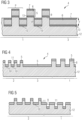
- FIG. 12 shows a longitudinal section through the security element 4 in order to show the structure of the sub-wavelength structure and the interference coating 5.
- FIG. The plane of the security element 4 thus runs horizontally here.
- the first sub-wavelength structure is provided in the first surface area 1 . It consists of columns 8, which are repeated periodically, each with a period P, in two directions. Only the period P in the direction from left to right in the plane of the drawing can be seen here. The period in the direction normal to the plane of the drawing may be the same as or different from that in the plane of the drawing.
- the height of the columns 8 corresponds to the effective depth T of the sub-wavelength structure.
- the pillars 8 can have any desired cross-section, such as circular, oval, rectangular or square. The cross section should ideally be constant over the height of the column 8, as far as this is technically possible.
- the dielectric layer 6 is then applied to this reflection layer 13 .
- the absorber layer 7 is applied to the dielectric layer 6 .
- the reflective layer 13 could be omitted.
- a coating or lamination can then be applied to the absorber layer 7 .
- the generally metallic reflection layer 13 of the interference coating 5 can also stimulate plasmonic effects.
- the light would strike the security element from above, and the color effect that is caused by the sub-wavelength structure together with the interference coating would be visible in the reflected light, ie from above.
- the light could also strike the security element from below (if the carrier substrate 12 is translucent).
- the color effect caused by the sub-wavelength structure would also be visible in the reflected light, ie from below.
- a color effect in transmission (if the carrier substrate 12 is translucent) cannot be ruled out.
- the fourth sub-wavelength structure 4 shows a longitudinal section through a security element 4, which has two different sub-wavelength structures.
- the first sub-wavelength structure is provided in the first surface area 1 .
- a second sub-wavelength structure is provided in the second surface area 2, which differs from the first in that its columns 11 are less high and less wide. These columns 11 are also repeated periodically in two directions, each with a period that can be the same as or different from that normal to the plane of the drawing.
- the period of the sub-wavelength structure of the first surface area 1 can be different from that of the second surface area 2 .
- the two surface areas 1, 2 with sub-wavelength structures are separated by a non-structured surface area 3 without sub-wavelength structures. All three surface areas 1-3 are provided with the same interference coating 5.
- non-structured surface area 3 could also be omitted, so that the first 1 and second surface area 2 directly adjoin one another. It can further surface areas with another sub-wavelength structure can also be provided.
- figure 5 shows a longitudinal section through a security element 4, which has two different sub-wavelength structures.
- both sub-wavelength structures are constructed using the same structural elements, namely columns 11, the columns 11, which are repeated periodically in two directions in the plane of the security element 4, are aligned in the first surface area 1 toward a first surface of the security element 4 and in the second surface area 2 toward a second surface of the security element 4, which is opposite the first surface.
- Both surface areas 1.2 are provided with the same interference coating 5.
- the two surface areas 1, 2 with sub-wavelength structures could also be separated by a non-structured surface area 3 without sub-wavelength structures.
- the sub-wavelength structure of the second surface area 2 corresponds to that of FIG 4 .
- the sub-wavelength structure of the first surface area 1 is mirrored here to that of the second surface area 2, specifically about a plane that is horizontal here.
- the columns 11 of the first surface area 1 are directed downwards here and arise when the depressions in the carrier substrate 12 are filled.
- the plane of the top surfaces 9 of the columns 11 in the first surface area 1 lies here in the plane of the surrounding surfaces 10 of the columns 11 in the second surface area 1.
Claims (11)
- Élément de sécurité plan (4) avec caractéristiques de sécurité optiques, comprenant au moins une première zone de surface (1) munie d'une première structure de sous-longueur d'onde, dans lequel les éléments de structure qui définissent la première structure de sous-longueur d'onde se répètent périodiquement dans le plan de l'élément de sécurité (4), dans lequel la première structure de sous-longueur d'onde d'au moins une partie de zone de la première zone de surface (1) est munie en outre d'un revêtement d'interférence (5) destiné à produire un effet de variation des couleurs, caractérisé en ce qu'à la limite d'une première zone de surface (1), il y a une zone de surface non structurée (3) qui ne présente pas de structure de sous-longueur d'onde mais présente, dans au moins une partie de zone, le même revêtement d'interférence (5) que dans au moins une partie de zone de la première zone de surface (1), la première zone de surface (1) et la zone de surface non structurée (3) produisant un motif grâce à au moins deux impressions colorées différentes.
- Élément de sécurité plan (4) selon la revendication 1, caractérisé en ce qu'il comprend, outre une première zone de surface (1) munie d'une première structure de sous-longueur d'onde, au moins une deuxième zone de surface (2) avec une deuxième structure de sous-longueur d'onde, la première zone de surface (1) étant disposée à côté de la deuxième zone de surface (2), les éléments de structure qui définissent la première structure de sous-longueur d'onde et la deuxième et qui se répètent périodiquement dans le plan de l'élément de sécurité (4) étant différents pour les deux zones de surface.
- Élément de sécurité plan (4) selon la revendication 1, caractérisé en ce qu'il comprend, outre une première zone de surface (1) avec une première structure de sous-longueur d'onde, au moins une deuxième zone de surface (2) avec une deuxième structure de sous-longueur d'onde, la première zone de surface (1) étant disposée à côté de la deuxième zone de surface (2), les éléments de structure qui définissent la première structure de sous-longueur d'onde et la deuxième et qui se répètent périodiquement dans le plan de l'élément de sécurité (4) étant les mêmes pour les deux zones de surface mais étant orientés vers une première surface de l'élément de sécurité dans la première zone de surface (1) et vers une deuxième surface de l'élément de sécurité, faisant face à la première surface, dans la deuxième zone de surface (2).
- Élément de sécurité plan (4) selon la revendication 2 ou 3, caractérisé en ce que la deuxième structure de sous-longueur d'onde d'au moins une partie de la deuxième zone de surface (2) est munie en outre d'un revêtement d'interférence (5) destiné à produire un effet de variation des couleurs.
- Élément de sécurité plan (4) selon l'une des revendications précédentes, caractérisé en ce que la première structure de sous-longueur d'onde d'une première zone de surface (1) et/ou, le cas échéant, la deuxième structure de sous-longueur d'onde d'une deuxième zone de surface (2) présentent côte à côte deux ou plusieurs revêtements d'interférence (5) différents pour produire un effet de variation des couleurs.
- Élément de sécurité plan (4) selon l'une des revendications 2 à 5, caractérisé en ce qu'au moins une première zone de surface (1) est disposée à la limite d'une deuxième zone de surface (2).
- Élément de sécurité plan (4) selon l'une des revendications 2 à 6, caractérisé en ce que la première zone de surface (1) est disposée à distance de la deuxième zone de surface (2), une zone de surface non structurée (3) dépourvue de structure de sous-longueur d'onde se trouvant entre la première zone de surface et la deuxième.
- Élément de sécurité plan (4) selon l'une des revendications 2 à 7, caractérisé en ce que les éléments de structure qui définissent la première structure de sous-longueur d'onde et la deuxième comprennent des colonnes (8, 11) ou des trous et le plan des aires de couverture des colonnes (8, 11) dans la première zone de surface (1) du plan correspond au plan des aires environnantes des colonnes (8, 11) dans la deuxième zone de surface (2) ou en ce que le plan des fonds des trous dans la première zone de surface (1) correspond au plan des surfaces entourant les trous dans la deuxième zone de surface (2).
- Élément de sécurité plan (4) selon l'une des revendications précédentes, caractérisé en ce que le revêtement d'interférence (5) est appliqué directement sur la structure de sous-longueur d'onde au moins dans une zone de surface (1, 2).
- Élément de sécurité plan (4) selon l'une des revendications précédentes, caractérisé en ce que la profondeur efficace (T) de la structure de sous-longueur d'onde est plus petite que l'épaisseur du revêtement d'interférence (5).
- Support de données ou document de valeur présentant un élément de sécurité selon l'une des revendications 1 à 10.
Applications Claiming Priority (2)
| Application Number | Priority Date | Filing Date | Title |
|---|---|---|---|
| ATA50225/2020A AT523690B1 (de) | 2020-03-16 | 2020-03-16 | Flächiges Sicherheitselement mit optischen Sicherheitsmerkmalen |
| PCT/EP2021/056474 WO2021185729A1 (fr) | 2020-03-16 | 2021-03-15 | Élément de sécurité plat présentant des caractéristiques de sécurité optique |
Publications (3)
| Publication Number | Publication Date |
|---|---|
| EP4121299A1 EP4121299A1 (fr) | 2023-01-25 |
| EP4121299B1 true EP4121299B1 (fr) | 2023-07-26 |
| EP4121299C0 EP4121299C0 (fr) | 2023-07-26 |
Family
ID=74947374
Family Applications (1)
| Application Number | Title | Priority Date | Filing Date |
|---|---|---|---|
| EP21712759.6A Active EP4121299B1 (fr) | 2020-03-16 | 2021-03-15 | Élément de sécurité plat présentant des caractéristiques de sécurité optique |
Country Status (6)
| Country | Link |
|---|---|
| US (1) | US20230125767A1 (fr) |
| EP (1) | EP4121299B1 (fr) |
| JP (1) | JP2023523383A (fr) |
| AT (1) | AT523690B1 (fr) |
| CA (1) | CA3169081A1 (fr) |
| WO (1) | WO2021185729A1 (fr) |
Families Citing this family (1)
| Publication number | Priority date | Publication date | Assignee | Title |
|---|---|---|---|---|
| FR3135013A1 (fr) * | 2022-04-27 | 2023-11-03 | Idemia France | Document de sécurité utilisable pour visualiser une image comprenant un film plasmonique avec des perforations |
Family Cites Families (18)
| Publication number | Priority date | Publication date | Assignee | Title |
|---|---|---|---|---|
| AT413360B (de) | 2002-08-06 | 2006-02-15 | Hueck Folien Gmbh | Verfahren zur herstellung von fälschungssicheren identifikationsmerkmalen |
| DE102007061979A1 (de) * | 2007-12-21 | 2009-06-25 | Giesecke & Devrient Gmbh | Sicherheitselement |
| DE102009012300A1 (de) * | 2009-03-11 | 2010-09-16 | Giesecke & Devrient Gmbh | Sicherheitselement mit mehrfarbigem Bild |
| DE102009041583A1 (de) * | 2009-09-15 | 2011-03-17 | Giesecke & Devrient Gmbh | Dünnschichtelement mit Interferenzschichtaufbau |
| DE102009056933A1 (de) * | 2009-12-04 | 2011-06-09 | Giesecke & Devrient Gmbh | Sicherheitselement mit Farbfilter, Wertdokument mit so einem solchen Sicherheitselement sowie Herstellungsverfahren eines solchen Sicherheitselementes |
| DE102010050895A1 (de) | 2010-11-10 | 2012-05-10 | Giesecke & Devrient Gmbh | Dünnschichtelement mit Mehrschichtstruktur |
| DE102011115589A1 (de) * | 2011-10-11 | 2013-04-11 | Giesecke & Devrient Gmbh | Sicherheitselement |
| DE102012015900A1 (de) * | 2012-08-10 | 2014-03-06 | Giesecke & Devrient Gmbh | Sicherheitselement mit farbeffekterzeugendem Gitter |
| DE102013108666A1 (de) * | 2013-08-09 | 2015-03-05 | Leonhard Kurz Stiftung & Co. Kg | Verfahren zur Herstellung eines Mehrschichtkörpers sowie Mehrschichtkörper |
| FR3014366B1 (fr) * | 2013-12-05 | 2016-01-08 | Continental Automotive France | Procede de determination de l'empreinte d'un pneumatique de roue sur le sol |
| DE102014010751A1 (de) * | 2014-07-21 | 2016-01-21 | Giesecke & Devrient Gmbh | Sicherheitselement mit Subwellenlängengitter |
| DE102014018551A1 (de) * | 2014-12-15 | 2016-06-16 | Giesecke & Devrient Gmbh | Wertdokument |
| JP6520359B2 (ja) * | 2015-04-30 | 2019-05-29 | 凸版印刷株式会社 | 表示体、物品、原版、および、原版の製造方法 |
| DE102015010191A1 (de) * | 2015-08-06 | 2017-02-09 | Giesecke & Devrient Gmbh | Sicherheitselement mit Subwellenlängengitter |
| KR102419708B1 (ko) * | 2016-06-24 | 2022-07-11 | 도판 인사츠 가부시키가이샤 | 광학 디바이스, 표시체, 표시체 부착 디바이스, 광학 필터, 및 광학 디바이스의 제조 방법 |
| DE102016013683A1 (de) * | 2016-11-16 | 2018-05-17 | Giesecke+Devrient Currency Technology Gmbh | Sicherheitselement mit Subwellenlängengitter |
| DE102016013690A1 (de) * | 2016-11-16 | 2018-05-17 | Giesecke+Devrient Currency Technology Gmbh | Sicherheitselement mit Subwellenlängengitter |
| DE102017130588A1 (de) * | 2017-12-19 | 2019-06-19 | Giesecke+Devrient Currency Technology Gmbh | Wertdokument |
-
2020
- 2020-03-16 AT ATA50225/2020A patent/AT523690B1/de active
-
2021
- 2021-03-15 JP JP2022555739A patent/JP2023523383A/ja active Pending
- 2021-03-15 EP EP21712759.6A patent/EP4121299B1/fr active Active
- 2021-03-15 WO PCT/EP2021/056474 patent/WO2021185729A1/fr active Application Filing
- 2021-03-15 US US17/911,752 patent/US20230125767A1/en active Pending
- 2021-03-15 CA CA3169081A patent/CA3169081A1/fr active Pending
Also Published As
| Publication number | Publication date |
|---|---|
| AT523690A1 (de) | 2021-10-15 |
| US20230125767A1 (en) | 2023-04-27 |
| EP4121299C0 (fr) | 2023-07-26 |
| CA3169081A1 (fr) | 2021-09-23 |
| JP2023523383A (ja) | 2023-06-05 |
| EP4121299A1 (fr) | 2023-01-25 |
| AT523690B1 (de) | 2022-03-15 |
| WO2021185729A1 (fr) | 2021-09-23 |
Similar Documents
| Publication | Publication Date | Title |
|---|---|---|
| EP2501553B1 (fr) | Elément de sûreté à microstructure | |
| EP2708371B1 (fr) | Elément de sécurité optique variable avec effet visuel supplémentaire de réflexion/transmission | |
| DE102012020550A1 (de) | Optisch variables Flächenmuster | |
| EP2953798A1 (fr) | Dessin de surface à variabilité optique | |
| EP3820715B1 (fr) | Element de securite optiquement variable avec zone de surface reflectif | |
| WO2009012893A2 (fr) | Élément de sécurité | |
| WO2013079542A2 (fr) | Élément optiquement variable | |
| DE102014019088A1 (de) | Optisch variables Durchsichtssicherheitselement | |
| EP3302995B1 (fr) | Élément de sécurité optiquement variable | |
| EP3337674A1 (fr) | Document de valeur | |
| EP4121299B1 (fr) | Élément de sécurité plat présentant des caractéristiques de sécurité optique | |
| EP3727870B1 (fr) | Élément de sécurité comprenant une nanostructure à deux dimensions et procédé de fabrication pour cet élément de sécurité | |
| AT523060B1 (de) | Sicherheitselement | |
| EP4275912A1 (fr) | Élément de sécurité | |
| EP4275911A1 (fr) | Élément de sécurité | |
| AT523814B1 (de) | Sicherheitselement | |
| WO2017025175A1 (fr) | Élément de sécurité | |
| EP3954544A1 (fr) | Élément de sécurité plat ayant des caractéristiques de sécurité optiques | |
| WO2021063702A1 (fr) | Élément de sécurité doté d'une couche à effet optique formée sous la forme d'une couche mince | |
| EP3606766A1 (fr) | Élément de sécurité et procédé de fabrication associé | |
| EP4306328A1 (fr) | Élément de sécurité |
Legal Events
| Date | Code | Title | Description |
|---|---|---|---|
| STAA | Information on the status of an ep patent application or granted ep patent |
Free format text: STATUS: UNKNOWN |
|
| STAA | Information on the status of an ep patent application or granted ep patent |
Free format text: STATUS: THE INTERNATIONAL PUBLICATION HAS BEEN MADE |
|
| PUAI | Public reference made under article 153(3) epc to a published international application that has entered the european phase |
Free format text: ORIGINAL CODE: 0009012 |
|
| STAA | Information on the status of an ep patent application or granted ep patent |
Free format text: STATUS: REQUEST FOR EXAMINATION WAS MADE |
|
| 17P | Request for examination filed |
Effective date: 20221013 |
|
| AK | Designated contracting states |
Kind code of ref document: A1 Designated state(s): AL AT BE BG CH CY CZ DE DK EE ES FI FR GB GR HR HU IE IS IT LI LT LU LV MC MK MT NL NO PL PT RO RS SE SI SK SM TR |
|
| GRAP | Despatch of communication of intention to grant a patent |
Free format text: ORIGINAL CODE: EPIDOSNIGR1 |
|
| STAA | Information on the status of an ep patent application or granted ep patent |
Free format text: STATUS: GRANT OF PATENT IS INTENDED |
|
| DAV | Request for validation of the european patent (deleted) | ||
| DAX | Request for extension of the european patent (deleted) | ||
| INTG | Intention to grant announced |
Effective date: 20230220 |
|
| TPAC | Observations filed by third parties |
Free format text: ORIGINAL CODE: EPIDOSNTIPA |
|
| GRAS | Grant fee paid |
Free format text: ORIGINAL CODE: EPIDOSNIGR3 |
|
| GRAA | (expected) grant |
Free format text: ORIGINAL CODE: 0009210 |
|
| STAA | Information on the status of an ep patent application or granted ep patent |
Free format text: STATUS: THE PATENT HAS BEEN GRANTED |
|
| AK | Designated contracting states |
Kind code of ref document: B1 Designated state(s): AL AT BE BG CH CY CZ DE DK EE ES FI FR GB GR HR HU IE IS IT LI LT LU LV MC MK MT NL NO PL PT RO RS SE SI SK SM TR |
|
| REG | Reference to a national code |
Ref country code: CH Ref legal event code: EP |
|
| REG | Reference to a national code |
Ref country code: IE Ref legal event code: FG4D Free format text: LANGUAGE OF EP DOCUMENT: GERMAN |
|
| REG | Reference to a national code |
Ref country code: DE Ref legal event code: R096 Ref document number: 502021001094 Country of ref document: DE |
|
| U01 | Request for unitary effect filed |
Effective date: 20230802 |
|
| U07 | Unitary effect registered |
Designated state(s): AT BE BG DE DK EE FI FR IT LT LU LV MT NL PT SE SI Effective date: 20230808 |
|
| REG | Reference to a national code |
Ref country code: LT Ref legal event code: MG9D |
|
| PG25 | Lapsed in a contracting state [announced via postgrant information from national office to epo] |
Ref country code: GR Free format text: LAPSE BECAUSE OF FAILURE TO SUBMIT A TRANSLATION OF THE DESCRIPTION OR TO PAY THE FEE WITHIN THE PRESCRIBED TIME-LIMIT Effective date: 20231027 |
|
| PG25 | Lapsed in a contracting state [announced via postgrant information from national office to epo] |
Ref country code: IS Free format text: LAPSE BECAUSE OF FAILURE TO SUBMIT A TRANSLATION OF THE DESCRIPTION OR TO PAY THE FEE WITHIN THE PRESCRIBED TIME-LIMIT Effective date: 20231126 |
|
| PG25 | Lapsed in a contracting state [announced via postgrant information from national office to epo] |
Ref country code: RS Free format text: LAPSE BECAUSE OF FAILURE TO SUBMIT A TRANSLATION OF THE DESCRIPTION OR TO PAY THE FEE WITHIN THE PRESCRIBED TIME-LIMIT Effective date: 20230726 Ref country code: NO Free format text: LAPSE BECAUSE OF FAILURE TO SUBMIT A TRANSLATION OF THE DESCRIPTION OR TO PAY THE FEE WITHIN THE PRESCRIBED TIME-LIMIT Effective date: 20231026 Ref country code: IS Free format text: LAPSE BECAUSE OF FAILURE TO SUBMIT A TRANSLATION OF THE DESCRIPTION OR TO PAY THE FEE WITHIN THE PRESCRIBED TIME-LIMIT Effective date: 20231126 Ref country code: HR Free format text: LAPSE BECAUSE OF FAILURE TO SUBMIT A TRANSLATION OF THE DESCRIPTION OR TO PAY THE FEE WITHIN THE PRESCRIBED TIME-LIMIT Effective date: 20230726 Ref country code: GR Free format text: LAPSE BECAUSE OF FAILURE TO SUBMIT A TRANSLATION OF THE DESCRIPTION OR TO PAY THE FEE WITHIN THE PRESCRIBED TIME-LIMIT Effective date: 20231027 |
|
| PG25 | Lapsed in a contracting state [announced via postgrant information from national office to epo] |
Ref country code: PL Free format text: LAPSE BECAUSE OF FAILURE TO SUBMIT A TRANSLATION OF THE DESCRIPTION OR TO PAY THE FEE WITHIN THE PRESCRIBED TIME-LIMIT Effective date: 20230726 |
|
| U20 | Renewal fee paid [unitary effect] |
Year of fee payment: 4 Effective date: 20240312 |
|
| PG25 | Lapsed in a contracting state [announced via postgrant information from national office to epo] |
Ref country code: ES Free format text: LAPSE BECAUSE OF FAILURE TO SUBMIT A TRANSLATION OF THE DESCRIPTION OR TO PAY THE FEE WITHIN THE PRESCRIBED TIME-LIMIT Effective date: 20230726 |
|
| PG25 | Lapsed in a contracting state [announced via postgrant information from national office to epo] |
Ref country code: SM Free format text: LAPSE BECAUSE OF FAILURE TO SUBMIT A TRANSLATION OF THE DESCRIPTION OR TO PAY THE FEE WITHIN THE PRESCRIBED TIME-LIMIT Effective date: 20230726 Ref country code: RO Free format text: LAPSE BECAUSE OF FAILURE TO SUBMIT A TRANSLATION OF THE DESCRIPTION OR TO PAY THE FEE WITHIN THE PRESCRIBED TIME-LIMIT Effective date: 20230726 Ref country code: ES Free format text: LAPSE BECAUSE OF FAILURE TO SUBMIT A TRANSLATION OF THE DESCRIPTION OR TO PAY THE FEE WITHIN THE PRESCRIBED TIME-LIMIT Effective date: 20230726 Ref country code: CZ Free format text: LAPSE BECAUSE OF FAILURE TO SUBMIT A TRANSLATION OF THE DESCRIPTION OR TO PAY THE FEE WITHIN THE PRESCRIBED TIME-LIMIT Effective date: 20230726 Ref country code: SK Free format text: LAPSE BECAUSE OF FAILURE TO SUBMIT A TRANSLATION OF THE DESCRIPTION OR TO PAY THE FEE WITHIN THE PRESCRIBED TIME-LIMIT Effective date: 20230726 |
|
| PLBI | Opposition filed |
Free format text: ORIGINAL CODE: 0009260 |