EP4120567B1 - Kaskadierte gate-treiberausgänge für stromwandlerschaltungen - Google Patents
Kaskadierte gate-treiberausgänge für stromwandlerschaltungen Download PDFInfo
- Publication number
- EP4120567B1 EP4120567B1 EP22163945.3A EP22163945A EP4120567B1 EP 4120567 B1 EP4120567 B1 EP 4120567B1 EP 22163945 A EP22163945 A EP 22163945A EP 4120567 B1 EP4120567 B1 EP 4120567B1
- Authority
- EP
- European Patent Office
- Prior art keywords
- power
- disconnect switch
- control signal
- power disconnect
- gate
- Prior art date
- Legal status (The legal status is an assumption and is not a legal conclusion. Google has not performed a legal analysis and makes no representation as to the accuracy of the status listed.)
- Active
Links
Images






Classifications
-
- H—ELECTRICITY
- H03—ELECTRONIC CIRCUITRY
- H03K—PULSE TECHNIQUE
- H03K17/00—Electronic switching or gating, i.e. not by contact-making and –breaking
- H03K17/28—Modifications for introducing a time delay before switching
- H03K17/284—Modifications for introducing a time delay before switching in field effect transistor switches
-
- H—ELECTRICITY
- H02—GENERATION; CONVERSION OR DISTRIBUTION OF ELECTRIC POWER
- H02M—APPARATUS FOR CONVERSION BETWEEN AC AND AC, BETWEEN AC AND DC, OR BETWEEN DC AND DC, AND FOR USE WITH MAINS OR SIMILAR POWER SUPPLY SYSTEMS; CONVERSION OF DC OR AC INPUT POWER INTO SURGE OUTPUT POWER; CONTROL OR REGULATION THEREOF
- H02M1/00—Details of apparatus for conversion
- H02M1/08—Circuits specially adapted for the generation of control voltages for semiconductor devices incorporated in static converters
-
- G—PHYSICS
- G01—MEASURING; TESTING
- G01R—MEASURING ELECTRIC VARIABLES; MEASURING MAGNETIC VARIABLES
- G01R19/00—Arrangements for measuring currents or voltages or for indicating presence or sign thereof
- G01R19/145—Indicating the presence of current or voltage
-
- H—ELECTRICITY
- H02—GENERATION; CONVERSION OR DISTRIBUTION OF ELECTRIC POWER
- H02M—APPARATUS FOR CONVERSION BETWEEN AC AND AC, BETWEEN AC AND DC, OR BETWEEN DC AND DC, AND FOR USE WITH MAINS OR SIMILAR POWER SUPPLY SYSTEMS; CONVERSION OF DC OR AC INPUT POWER INTO SURGE OUTPUT POWER; CONTROL OR REGULATION THEREOF
- H02M1/00—Details of apparatus for conversion
- H02M1/0003—Details of control, feedback or regulation circuits
- H02M1/0029—Circuits or arrangements for limiting the slope of switching signals, e.g. slew rate
-
- H—ELECTRICITY
- H02—GENERATION; CONVERSION OR DISTRIBUTION OF ELECTRIC POWER
- H02M—APPARATUS FOR CONVERSION BETWEEN AC AND AC, BETWEEN AC AND DC, OR BETWEEN DC AND DC, AND FOR USE WITH MAINS OR SIMILAR POWER SUPPLY SYSTEMS; CONVERSION OF DC OR AC INPUT POWER INTO SURGE OUTPUT POWER; CONTROL OR REGULATION THEREOF
- H02M1/00—Details of apparatus for conversion
- H02M1/32—Means for protecting converters other than automatic disconnection
-
- H—ELECTRICITY
- H02—GENERATION; CONVERSION OR DISTRIBUTION OF ELECTRIC POWER
- H02M—APPARATUS FOR CONVERSION BETWEEN AC AND AC, BETWEEN AC AND DC, OR BETWEEN DC AND DC, AND FOR USE WITH MAINS OR SIMILAR POWER SUPPLY SYSTEMS; CONVERSION OF DC OR AC INPUT POWER INTO SURGE OUTPUT POWER; CONTROL OR REGULATION THEREOF
- H02M1/00—Details of apparatus for conversion
- H02M1/36—Means for starting or stopping converters
-
- H—ELECTRICITY
- H02—GENERATION; CONVERSION OR DISTRIBUTION OF ELECTRIC POWER
- H02M—APPARATUS FOR CONVERSION BETWEEN AC AND AC, BETWEEN AC AND DC, OR BETWEEN DC AND DC, AND FOR USE WITH MAINS OR SIMILAR POWER SUPPLY SYSTEMS; CONVERSION OF DC OR AC INPUT POWER INTO SURGE OUTPUT POWER; CONTROL OR REGULATION THEREOF
- H02M7/00—Conversion of AC power input into DC power output; Conversion of DC power input into AC power output
- H02M7/42—Conversion of DC power input into AC power output without possibility of reversal
- H02M7/44—Conversion of DC power input into AC power output without possibility of reversal by static converters
- H02M7/48—Conversion of DC power input into AC power output without possibility of reversal by static converters using discharge tubes with control electrode or semiconductor devices with control electrode
- H02M7/53—Conversion of DC power input into AC power output without possibility of reversal by static converters using discharge tubes with control electrode or semiconductor devices with control electrode using devices of a triode or transistor type requiring continuous application of a control signal
- H02M7/537—Conversion of DC power input into AC power output without possibility of reversal by static converters using discharge tubes with control electrode or semiconductor devices with control electrode using devices of a triode or transistor type requiring continuous application of a control signal using semiconductor devices only, e.g. single switched pulse inverters
- H02M7/5387—Conversion of DC power input into AC power output without possibility of reversal by static converters using discharge tubes with control electrode or semiconductor devices with control electrode using devices of a triode or transistor type requiring continuous application of a control signal using semiconductor devices only, e.g. single switched pulse inverters in a bridge configuration
- H02M7/53871—Conversion of DC power input into AC power output without possibility of reversal by static converters using discharge tubes with control electrode or semiconductor devices with control electrode using devices of a triode or transistor type requiring continuous application of a control signal using semiconductor devices only, e.g. single switched pulse inverters in a bridge configuration with automatic control of output voltage or current
- H02M7/53873—Conversion of DC power input into AC power output without possibility of reversal by static converters using discharge tubes with control electrode or semiconductor devices with control electrode using devices of a triode or transistor type requiring continuous application of a control signal using semiconductor devices only, e.g. single switched pulse inverters in a bridge configuration with automatic control of output voltage or current with digital control
-
- H—ELECTRICITY
- H02—GENERATION; CONVERSION OR DISTRIBUTION OF ELECTRIC POWER
- H02P—CONTROL OR REGULATION OF ELECTRIC MOTORS, ELECTRIC GENERATORS OR DYNAMO-ELECTRIC CONVERTERS; CONTROLLING TRANSFORMERS, REACTORS OR CHOKE COILS
- H02P27/00—Arrangements or methods for the control of AC motors characterised by the kind of supply voltage
- H02P27/04—Arrangements or methods for the control of AC motors characterised by the kind of supply voltage using variable-frequency supply voltage, e.g. inverter or converter supply voltage
- H02P27/06—Arrangements or methods for the control of AC motors characterised by the kind of supply voltage using variable-frequency supply voltage, e.g. inverter or converter supply voltage using DC to AC converters or inverters
-
- H—ELECTRICITY
- H03—ELECTRONIC CIRCUITRY
- H03K—PULSE TECHNIQUE
- H03K17/00—Electronic switching or gating, i.e. not by contact-making and –breaking
- H03K17/06—Modifications for ensuring a fully conducting state
- H03K17/063—Modifications for ensuring a fully conducting state in field-effect transistor switches
-
- H—ELECTRICITY
- H03—ELECTRONIC CIRCUITRY
- H03K—PULSE TECHNIQUE
- H03K17/00—Electronic switching or gating, i.e. not by contact-making and –breaking
- H03K17/12—Modifications for increasing the maximum permissible switched current
- H03K17/122—Modifications for increasing the maximum permissible switched current in field-effect transistor switches
-
- H—ELECTRICITY
- H03—ELECTRONIC CIRCUITRY
- H03K—PULSE TECHNIQUE
- H03K17/00—Electronic switching or gating, i.e. not by contact-making and –breaking
- H03K17/16—Modifications for eliminating interference voltages or currents
- H03K17/161—Modifications for eliminating interference voltages or currents in field-effect transistor switches
- H03K17/162—Modifications for eliminating interference voltages or currents in field-effect transistor switches without feedback from the output circuit to the control circuit
- H03K17/163—Soft switching
- H03K17/164—Soft switching using parallel switching arrangements
-
- H—ELECTRICITY
- H03—ELECTRONIC CIRCUITRY
- H03K—PULSE TECHNIQUE
- H03K17/00—Electronic switching or gating, i.e. not by contact-making and –breaking
- H03K17/16—Modifications for eliminating interference voltages or currents
- H03K17/161—Modifications for eliminating interference voltages or currents in field-effect transistor switches
- H03K17/165—Modifications for eliminating interference voltages or currents in field-effect transistor switches by feedback from the output circuit to the control circuit
- H03K17/166—Soft switching
- H03K17/167—Soft switching using parallel switching arrangements
-
- H—ELECTRICITY
- H03—ELECTRONIC CIRCUITRY
- H03K—PULSE TECHNIQUE
- H03K17/00—Electronic switching or gating, i.e. not by contact-making and –breaking
- H03K17/51—Electronic switching or gating, i.e. not by contact-making and –breaking characterised by the components used
- H03K17/56—Electronic switching or gating, i.e. not by contact-making and –breaking characterised by the components used by the use, as active elements, of semiconductor devices
- H03K17/687—Electronic switching or gating, i.e. not by contact-making and –breaking characterised by the components used by the use, as active elements, of semiconductor devices the devices being field-effect transistors
- H03K17/6871—Electronic switching or gating, i.e. not by contact-making and –breaking characterised by the components used by the use, as active elements, of semiconductor devices the devices being field-effect transistors the output circuit comprising more than one controlled field-effect transistor
-
- H—ELECTRICITY
- H02—GENERATION; CONVERSION OR DISTRIBUTION OF ELECTRIC POWER
- H02M—APPARATUS FOR CONVERSION BETWEEN AC AND AC, BETWEEN AC AND DC, OR BETWEEN DC AND DC, AND FOR USE WITH MAINS OR SIMILAR POWER SUPPLY SYSTEMS; CONVERSION OF DC OR AC INPUT POWER INTO SURGE OUTPUT POWER; CONTROL OR REGULATION THEREOF
- H02M1/00—Details of apparatus for conversion
- H02M1/08—Circuits specially adapted for the generation of control voltages for semiconductor devices incorporated in static converters
- H02M1/088—Circuits specially adapted for the generation of control voltages for semiconductor devices incorporated in static converters for the simultaneous control of series or parallel connected semiconductor devices
-
- H—ELECTRICITY
- H02—GENERATION; CONVERSION OR DISTRIBUTION OF ELECTRIC POWER
- H02M—APPARATUS FOR CONVERSION BETWEEN AC AND AC, BETWEEN AC AND DC, OR BETWEEN DC AND DC, AND FOR USE WITH MAINS OR SIMILAR POWER SUPPLY SYSTEMS; CONVERSION OF DC OR AC INPUT POWER INTO SURGE OUTPUT POWER; CONTROL OR REGULATION THEREOF
- H02M7/00—Conversion of AC power input into DC power output; Conversion of DC power input into AC power output
- H02M7/42—Conversion of DC power input into AC power output without possibility of reversal
- H02M7/44—Conversion of DC power input into AC power output without possibility of reversal by static converters
- H02M7/48—Conversion of DC power input into AC power output without possibility of reversal by static converters using discharge tubes with control electrode or semiconductor devices with control electrode
- H02M7/53—Conversion of DC power input into AC power output without possibility of reversal by static converters using discharge tubes with control electrode or semiconductor devices with control electrode using devices of a triode or transistor type requiring continuous application of a control signal
- H02M7/537—Conversion of DC power input into AC power output without possibility of reversal by static converters using discharge tubes with control electrode or semiconductor devices with control electrode using devices of a triode or transistor type requiring continuous application of a control signal using semiconductor devices only, e.g. single switched pulse inverters
- H02M7/5387—Conversion of DC power input into AC power output without possibility of reversal by static converters using discharge tubes with control electrode or semiconductor devices with control electrode using devices of a triode or transistor type requiring continuous application of a control signal using semiconductor devices only, e.g. single switched pulse inverters in a bridge configuration
Definitions
- Linear FETs have been proposed for limiting inrush current and equal current sharing during inrush transients when paralleled.
- Linear FET technology combines the low RDSon (on-state resistance) of a trench MOSFET with the wide safe operating area (SOA) of a planar MOSFET.
- SOA wide safe operating area
- US 2015 / 0 381 056 A1 discloses a switched-mode power supply device including an AC power supply, a transformer having a primary winding and a secondary winding, a switching element electrically connected to the primary winding, a secondary-side rectifying and smoothing circuit that generates an output voltage by rectifying and smoothing the pulse voltage, a load ratio detection circuit that detects if a load ratio is not greater than a load ratio threshold value during steady load, and outputs a drive switch signal based on the detection, and a drive circuit that, on the basis of the drive switch signal, causes the switching element to perform switching operation in one of a normal drive in which a speed of charging agate voltage is faster and a soft drive in which the speed of charging the gate voltage is slower.
- the embodiments described herein provide a gate driver circuit with two or more outputs and having configurable turn on and/or configurable turn off delay introduced between the outputs such that a first power disconnect switch turns on first to limit the inrush current during power on events and a second power disconnect switch with a delayed turn on time relative to the first power disconnect switch to reduce system power losses during normal operation. Similar delayed sequencing may occur during turn off events in that the first power disconnect switch may turn off first followed by the second power disconnect switch to provide a controlled turn off at high currents which avoids avalanching of the disconnect switch.
- the delay may be introduced in the gate driver by analog or digital implementation and may be programmable or defined by measurement, calibration, etc. or may be fixed.
- inrush current sensing may be implemented via a series resistor or RDSon sensing using a comparator.
- the second power disconnect switch may be turned on.
- the turn-on delay implemented by the gate driver circuit instead may be a constant value such that no additional sense circuitry is needed.
- the first power disconnect switch is turned off immediately in response to system or controller protection or a normal shutdown sequence.
- the second power disconnect switch may be turned off in a controlled manner after a delay from when the first power disconnect switch is turned off, to avoid avalanching.
- just the turn on delay may be implemented.
- just the turn off delay may be implemented.
- both the turn on delay and the turn off delay may be implemented.
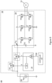
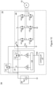
- Figure 1 illustrates an embodiment of an electronic system 100 that includes a load 102, a power source 104, and power conversion circuit 106 coupled between the load 102 and the power source 104. Whether power inversion or conversion occurs between the power source 104 and the load 102 depends on the type of electronic system 100.
- the power source 104 is a battery 'V BAT '
- the load 102 is a multi-phase motor 'M'
- the power conversion circuit 106 inverts a DC voltage from the battery V BAT to an ac voltage applied to the multi-phase motor M.
- the motor may be a 3-phase motor and the power conversion circuit 106 may include three half bridges each including a high-side power transistor HSn coupled in series to a low-side power transistor LSn between a power input node P IN of an inverter/converter 108 and ground to form a respective phase input ⁇ n to the 3-phase motor M.
- the inverter/converter 108 functions as an inverter.
- the power source 104 is instead an ac source
- the inverter/converter 108 functions as a converter.
- the inverter/converter 108 may have other configurations such as full bridge, synchronous rectifier, etc., depending on the type of application.
- the power conversion circuit 106 also includes a bulk or dc bus capacitor C DC electrically coupled to the power input node P IN of the inverter/converter 108.
- the power conversion circuit 106 further includes at least one first transistor T1a electrically coupled between the power source 104 and the power input node P IN of the inverter/converter 108, and at least one second transistor T2a in parallel with the at least one first transistor T1a and electrically coupled between the power source 104 and the power input node P IN of the inverter/converter 108.
- the power conversion circuit 106 further includes a controller 110 such as a microcontroller, CPU (central processing unit), etc. that operates the at least one first transistor T1a and the at least one second transistor T2a as respective first and second disconnect switches 112, 114 when disconnecting the power source 104 from the load 102, e.g., as part of hot swap, electronic fuse and/or battery protection applications.
- a controller 110 such as a microcontroller, CPU (central processing unit), etc. that operates the at least one first transistor T1a and the at least one second transistor T2a as respective first and second disconnect switches 112, 114 when disconnecting the power source 104 from the load 102, e.g., as part of hot swap, electronic fuse and/or battery protection applications.
- the at least one first transistor T1a that forms the first disconnect switch 112 is a different type of transistor or a transistor with a different type of operating characteristic (e.g., gate charge) compared to the at least one second transistor T2a that forms the second disconnect switch 114.
- the at least one first transistor T1a that forms the first disconnect switch 112 is better suited for limiting the inrush current flowing into the power input node P IN of the inverter/converter 108 during power on of the load 102 whereas the at least one second transistor T2a that forms the second disconnect switch 114 provides lower RDSon during normal operation of the load 102.
- the first power disconnect switch 112 is realized by a plurality of first transistors T1a... T1n coupled in parallel and controlled by the same first gate control signal 'A'.
- the second power disconnect switch 114 similarly may be realized by a plurality of second transistors T2a...T2m coupled in parallel and controlled by the same second gate control signal 'B'.
- one or both of the power disconnect switches 112, 114 may only include a single transistor.
- a gate driver circuit 116 of the power conversion circuit 106 generates the first gate control signal A for each first transistor T1a...T1n that forms the first power disconnect switch 112 and generates the second gate control signal B for each second transistor T2a...T2m that forms the second power disconnect switch 114.
- the gate driver circuit 116 When powering up the load 102, the gate driver circuit 116 generates the gate control signals A, B such that the second gate control signal B has a delayed turn on time compared to the first gate control signal A. Accordingly, each first transistor T1a...T1n of the first power disconnect switch 112 turns on before each second transistor T2a... T2m of the second power disconnect switch 114.
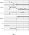
- Figure 2 illustrates various waveforms associated with powering-up the load 102.
- Figure 2 shows the first gate control signal A in volts (V), the second gate control signal B in volts (V), the gate-to-source voltage VGS1 of the first power disconnect switch 112 in volts (V), the gate-to-source voltage VGS2 of the second power disconnect switch 114 in volts (V), the drain-to-source voltage VDS1 of the first power disconnect switch 112 in volts (V), and the current I_P IN flowing into the power input node P IN of the inverter/converter 104 in amperes (A).
- the gate driver circuit 116 generates the gate control signals A, B such that the second gate control signal B has a delayed turn on time compared to the first gate control signal A when powering up the load 102. Accordingly, the gate-to-source voltage VGS1 of the first power disconnect switch 112 rises before the gate-to-source voltage VGS2 of the second power disconnect switch 114, causing the first power disconnect switch 112 to turn on and begin conducting current before the second power disconnect switch 114.
- current I_P IN begins flowing into the power input node P IN of the inverter/converter 104 as the bulk or dc bus capacitor C DC charges.
- each first transistor T1a...T1n of the first power disconnect switch 112 is a Linear FET and each second transistor T2a... T2m of the second power disconnect switch 114 is a transistor type other than a Linear FET like standard MOSFETs, e.g., a planar MOSFET or a trench MOSFET.
- Figure 3A plots gate charge characteristics for a typical trench MOSFET whereas Figure 3B plots gate charge characteristics for a Linear FET.
- the x-axis in both graphs represents gate charge (Qgate) in nano coulombs (nC) and the y-axis in both graphs represents gate-to-source voltage (V GS ) in volts (V).
- the gate charge characteristics are plotted for three different operating voltages: 20V, 50V and 80V.
- the Linear FET has a higher plateau voltage ( ⁇ 7V versus ⁇ 4.5V in this example) and a wider gate to drain charge capability.
- the Miller plateau can be reached for the Linear FET with a much lower charge (approximately 10 nC vs. approximately 55 nC) and the Linear FET enters linear mode more effortlessly.
- the Linear FET then stays in the plateau region longer due to higher gate to drain charge needed to completely charge the MOSFET (more than 130 nC vs. approximately 30 nC).
- first power disconnect switch 112 as one or more Linear FETs provides for a controlled turn-on, thereby limiting the inrush current I_inrush flowing into the power input node P IN of the inverter/converter 104. This is, however, just one example. Other transistor types may be used for the first power disconnect switch 112 to provide better inrush current control compared to the second power disconnect switch 112.
- the second power disconnect switch 112 may be optimized for low RDSon during normal operation. For example, a plurality of trench MOSFETs may be coupled in parallel to reduce RDSon during normal operation. Any threshold variation between the paralleled trench MOSFETs should have no effect on inrush current limiting capability during power on, since the gate driver circuit 116 delays the second gate control signal B applied to the second power disconnect switch 114 relative to the first gate control signal A applied to the first power disconnect switch 112. Accordingly, the first power disconnect switch 112 is switched on before the second power disconnect switch 114 and therefore handles/limits the inrush current I_inrush without contribution from the second power disconnect switch 114.
- the delay in the activation of the second gate control signal B is implemented such that the second power disconnect switch 114 turns on via the second gate control signal B after the peak inrush current I_pk subsides, e.g., as shown in Figure 2 .
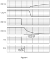
- each Linear FET is turned off first when powering down the load 102 so as to avoid fast turn off avalanching and/or excessive ringing across the drain-to-source voltage of the Linear FET(s).
- Turning off the second power disconnect switch 114 after the first power disconnect switch 112 has been turned off allows for a safe and controlled turn-off process.
- Implementing both the turn on delay and the turn off delay approaches in conjunction allows for inrush current control during power on of the load 102 and for safe/controlled powering down of the load 102.
- Example 31 A power conversion circuit, comprising: an inverter/converter; a bulk capacitor electrically coupled to a power input node of the inverter/converter; a first transistor electrically coupled between a power input node of the power conversion circuit and the power input node of the inverter/converter; a second transistor in parallel with the first transistor and electrically coupled between the power input node of the power conversion circuit and the power input node of the inverter/converter; a controller configured to operate the first transistor and the second transistor as disconnect switches when disconnecting the power input node of the power conversion circuit from the power input node of the inverter/converter; and a gate driver circuit configured to generate a first gate control signal for the first transistor and a second gate control signal for the second transistor, the second gate control signal having a delayed turn on time compared to the first gate control signal such that the first transistor turns on before the second transistor and the capacitor begins to draw an inrush current through the first transistor but not the second transistor.
Landscapes
- Engineering & Computer Science (AREA)
- Power Engineering (AREA)
- Physics & Mathematics (AREA)
- General Physics & Mathematics (AREA)
- Power Conversion In General (AREA)
Claims (10)
- Gatetreiberschaltung, die aufweist:wenigstens einen Treiber (120, 122; 502), der dazu ausgebildet ist, ein erstes Gatesteuersignal (A) für einen ersten Leistungstrennschalter (112) und ein zweites Gatesteuersignal (B) für einen zu dem ersten Leistungstrennschalter parallelen zweiten Leistungstrennschalter (114) (112) zu erzeugen; undeine Logik (124), die dazu ausgebildet ist, eine verzögerte Einschaltzeit für das zweite Gatesteuersignal (B) im Vergleich zu dem ersten Gatesteuersignal (A) derart zu implementieren, dass beim Einschalten einer mit dem ersten und dem zweiten Leistungstrennschalter (112, 114) gekoppelten Last (102) der erste Leistungstrennschalter (112) vor dem zweiten Leistungstrennschalter (114) einschaltet,dadurch gekennzeichnet, dassdie Logik (124) dazu ausgebildet ist, die verzögerte Einschaltzeit zu implementieren basierend aufeiner erfassten Drain-Source-Spannung des ersten Leistungstrennschalters (112) oder einem durch den ersten Leistungstrennschalter (112) fließenden erfassten Strom,einem durch einen zwischen einer Leistungsquelle (104) und dem ersten Leistungstrennschalter (112) gekoppelten Widerstand (RSEN) fließenden erfassten Strom,einer erfassten Spannung eines Kondensators (CDC) zwischen dem ersten Leistungstrennschalter (112) und Masse, oder,wenn die Last (102) ein Leistungsumwandlungssystem (108) ist, basierend auf einer erfassten Spannung eines Entkopplungs-Bulk-Kondensators oder eines DC-Bus-Kondensators (CDC) an einem Eingang des Leistungsumwandlungssystems (108), der geladen wird, wenn der erste Leistungstrennschalter (112) eingeschaltet wird.
- Gatetreiberschaltung nach Anspruch 1,wobei die Gatetreiberschaltung (116) einen einzelnen Treiber (502) aufweist,wobei der einzelne Treiber (502) dazu ausgebildet ist, das erste Gatesteuersignal (A) auszugeben, undwobei die Logik dazu ausgebildet ist, das zweite Gatesteuersignal (B) durch Anwenden der verzögerten Einschaltzeit auf den Ausgang des einzelnen Treibers (502) zu erzeugen.
- Gatetreiberschaltung nach Anspruch 1,wobei die Gatetreiberschaltung (116) einen ersten Treiber (120) und einen zweiten Treiber (122) aufweist,wobei der erste Treiber (120) dazu ausgebildet ist, das erste Gatesteuersignal (A) basierend auf einem von einem Controller erhaltenen Schaltsteuersignal zu erzeugen, undwobei die Logik (124) dazu ausgebildet ist, die verzögerte Einschaltzeit auf das Schaltsteuersignal zur Eingabe in den zweiten Treiber (122) anzuwenden.
- Gatetreiberschaltung nach einem der Ansprüche 1 bis 3, wobei die Logik (124) ferner dazu ausgebildet ist, eine verzögerte Ausschaltzeit für das zweite Gatesteuersignal (B) im Vergleich zu dem ersten Gatesteuersignal (A) derart zu implementieren, dass beim Ausschalten der mit dem ersten und dem zweiten Leistungstrennschalter (112, 114) gekoppelten Last (108) der erste Leistungstrennschalter (112) vor dem zweiten Leistungstrennschalter (114) ausschaltet.
- Gatetreiberschaltung nach Anspruch 4, wobei die verzögerte Ausschaltzeit derart ist, dass der erste Leistungstrennschalter (112) vollständig ausgeschaltet ist, bevor der zweite Leistungstrennschalter (114) mit dem Ausschalten beginnt.
- Gatetreiberschaltung nach Anspruch 4, wobei die verzögerte Ausschaltzeit derart ist, dass beim Ausschalten der mit dem ersten und dem zweiten Leistungstrennschalter (112, 114) gekoppelten Last der zweite Leistungstrennschalter (114) ein gesteuertes Ausschalten aufweist.
- Gatetreiberschaltung nach Anspruch 4, wobei die Logik (124) dazu ausgebildet ist, die verzögerte Ausschaltzeit basierend auf einem programmierten Verzögerungswert zu implementieren.
- Gatetreiberschaltung nach einem der Ansprüche 1 bis 7, wobei der erste Leistungstrennschalter (112) monolithisch mit der Gatetreiberschaltung (116) integriert ist.
- Leistungswandlungsschaltung, die aufweist:einen Wechselrichter/Wandler (108);einen Kondensator (CDC), der elektrisch an einen Leistungseingangsknoten des Wechselrichters/Wandlers (108) gekoppelt ist;einen ersten Transistor (T1a), der elektrisch zwischen einen Leistungseingangsknoten der Leistungswandlungsschaltung und den Leistungseingangsknoten des Wechselrichters/Wandlers (108) gekoppelt ist;
einen zu dem ersten Transistor (T1a) parallelen zweiten Transistor (T2a), der elektrisch zwischen den Leistungseingangsknoten der Leistungswandlungsschaltung und den Leistungseingangsknoten des Wechselrichters/Wandlers (108) gekoppelt ist;einen Controller (110), der dazu ausgebildet ist, den ersten Transistor (112) und den zweiten Transistor (114) als Trennschalter zu betreiben, wenn der Leistungseingangsknoten der Leistungswandlungsschaltung von dem Leistungseingangsknoten des Wechselrichters/Wandlers (108) getrennt wird; undeine Gatetreiberschaltung (116) nach einem der Ansprüche 1 bis 8, die dazu ausgebildet ist, ein erstes Gatesteuersignal (A) für den ersten Transistor (T1a) und ein zweites Gatesteuersignal (B) für den zweiten Transistor (T2a) zu erzeugen. - Verfahren zum Ansteuern eines ersten Leistungstrennschalters (112) und eines parallel zu dem ersten Leistungstrennschalter (112) gekoppelten zweiten Leistungstrennschalters (114), wobei das Verfahren aufweist:Erzeugen eines ersten Gatesteuersignals (A) für den ersten Leistungstrennschalter (112) und eines zweiten Gatesteuersignals (B) für den zweiten Leistungstrennschalter (114); undImplementieren einer verzögerten Einschaltzeit für das zweite Gatesteuersignal (B) im Vergleich zu dem ersten Gatesteuersignal (A) derart, dass beim Einschalten einer mit dem ersten und dem zweiten Leistungstrennschalter (102, 104) gekoppelten Last (102) der erste Leistungstrennschalter (112) vor dem zweiten Leistungstrennschalter (114) einschaltet,wobei das Implementieren der verzögerten Einschaltzeit das Implementieren der verzögerten Einschaltzeit aufweist basierend aufeiner erfassten Drain-Source-Spannung des ersten Leistungstrennschalters (112) oder einem durch den ersten Leistungstrennschalter (112) fließenden erfassten Strom,einem durch einen zwischen einer Leistungsquelle (104) und dem ersten Leistungstrennschalter (112) gekoppelten Widerstand (RSEN) fließenden erfassten Strom,einer erfassten Spannung eines Kondensators (CDC) zwischen dem ersten Leistungstrennschalter (112) und Masse, oder,wenn die Last (102) ein Leistungsumwandlungssystem (108) ist, basierend auf einer erfassten Spannung eines Entkopplungs-Bulk-Kondensators oder eines DC-Bus-Kondensators (CDC) an einem Eingang des Leistungsumwandlungssystems (108), der geladen wird, wenn der erste Leistungstrennschalter (112) eingeschaltet wird.
Applications Claiming Priority (1)
| Application Number | Priority Date | Filing Date | Title |
|---|---|---|---|
| US17/209,282 US11349474B1 (en) | 2021-03-23 | 2021-03-23 | Cascaded gate driver outputs for power conversion circuits |
Publications (2)
| Publication Number | Publication Date |
|---|---|
| EP4120567A1 EP4120567A1 (de) | 2023-01-18 |
| EP4120567B1 true EP4120567B1 (de) | 2025-07-09 |
Family
ID=80933825
Family Applications (1)
| Application Number | Title | Priority Date | Filing Date |
|---|---|---|---|
| EP22163945.3A Active EP4120567B1 (de) | 2021-03-23 | 2022-03-23 | Kaskadierte gate-treiberausgänge für stromwandlerschaltungen |
Country Status (3)
| Country | Link |
|---|---|
| US (1) | US11349474B1 (de) |
| EP (1) | EP4120567B1 (de) |
| CN (1) | CN115118133A (de) |
Families Citing this family (5)
| Publication number | Priority date | Publication date | Assignee | Title |
|---|---|---|---|---|
| CN115241941A (zh) * | 2021-04-23 | 2022-10-25 | 哈曼国际工业有限公司 | 用于由电池供电的可穿戴设备的电源电路 |
| US12542480B2 (en) * | 2023-04-13 | 2026-02-03 | Infineon Technologies Ag | Configuration techniques for gate drivers with reduced wiring |
| US20250323653A1 (en) * | 2024-04-16 | 2025-10-16 | Infineon Technologies Austria Ag | Self-calibrating delay line flash adc and tracking circuitry |
| US12549179B2 (en) | 2024-04-30 | 2026-02-10 | Nxp Usa, Inc. | Cascoded power switches usable in DC-DC converter applications |
| US20250337326A1 (en) * | 2024-04-30 | 2025-10-30 | Nxp Usa, Inc. | Cascoded power switches usable in dc-dc converter applications |
Family Cites Families (13)
| Publication number | Priority date | Publication date | Assignee | Title |
|---|---|---|---|---|
| US4356408A (en) * | 1980-08-01 | 1982-10-26 | Sundstrand Corporation | Drive circuit for parallel non-matched semiconductors |
| US6249111B1 (en) * | 2000-06-22 | 2001-06-19 | Intel Corporation | Dual drive buck regulator |
| US6930473B2 (en) * | 2001-08-23 | 2005-08-16 | Fairchild Semiconductor Corporation | Method and circuit for reducing losses in DC-DC converters |
| CN100527576C (zh) * | 2005-03-18 | 2009-08-12 | 株式会社理光 | 电源开关电路 |
| US7994769B2 (en) * | 2007-11-29 | 2011-08-09 | Rohm Co., Ltd. | Switching regulator and control circuit thereof |
| JP5342153B2 (ja) * | 2008-02-20 | 2013-11-13 | 矢崎総業株式会社 | モータ負荷制御装置 |
| US8884597B2 (en) * | 2012-07-20 | 2014-11-11 | Fairchild Semiconductor Corporation | Synchronous buck converter with dynamically adjustable low side gate driver |
| US9425792B2 (en) * | 2013-07-29 | 2016-08-23 | Texas Instruments Incorporated | Reconfigurable power switch chains for efficient dynamic power saving |
| JP2016027775A (ja) * | 2014-06-27 | 2016-02-18 | サンケン電気株式会社 | スイッチング電源装置 |
| JP6492965B2 (ja) * | 2015-05-22 | 2019-04-03 | 株式会社デンソー | パワートランジスタ駆動装置 |
| US9425691B1 (en) * | 2015-06-17 | 2016-08-23 | Cypress Semiconductor Corporation | Low thermal design for DC-DC converter |
| EP3590189B1 (de) * | 2017-03-02 | 2022-01-05 | HELLA GmbH & Co. KGaA | Hybridschaltersteuerung |
| US10459510B1 (en) * | 2019-01-17 | 2019-10-29 | Qualcomm Incorporated | Power chain with delay adaptive switches |
-
2021
- 2021-03-23 US US17/209,282 patent/US11349474B1/en active Active
-
2022
- 2022-03-22 CN CN202210286884.6A patent/CN115118133A/zh active Pending
- 2022-03-23 EP EP22163945.3A patent/EP4120567B1/de active Active
Also Published As
| Publication number | Publication date |
|---|---|
| EP4120567A1 (de) | 2023-01-18 |
| CN115118133A (zh) | 2022-09-27 |
| US11349474B1 (en) | 2022-05-31 |
Similar Documents
| Publication | Publication Date | Title |
|---|---|---|
| EP4120567A1 (de) | Kaskadierte gate-treiberausgänge für stromwandlerschaltungen | |
| US8040162B2 (en) | Switch matrix drive circuit for a power element | |
| CN104467370B (zh) | 用于隔离的驱动器的软关闭的设备和方法 | |
| US8754675B2 (en) | System and method for driving a switch | |
| US9203393B2 (en) | Semiconductor apparatus | |
| JP5315026B2 (ja) | 半導体装置 | |
| CN107979360B (zh) | 可配置电路及其操作方法和集成电路 | |
| KR20170041852A (ko) | 자기 소호형 반도체 소자의 단락 보호 회로 | |
| US20120133420A1 (en) | System and Method for Bootstrapping a Switch Driver | |
| US10642306B1 (en) | Gate driver circuit for reducing deadtime inefficiencies | |
| CN107852159B (zh) | 驱动装置 | |
| EP2993773A1 (de) | Bidirektionale strommessschaltung | |
| CN106533129B (zh) | 自举补偿电路及功率模块 | |
| EP3832866B1 (de) | Überstromschutzschaltung und schaltkreis | |
| US11621709B2 (en) | Power module with built-in drive circuits | |
| EP4629509A1 (de) | Leistungsschaltvorrichtung zur reduzierung des einschaltwiderstandes und zur verlängerung der kurzschlusswiderstandszeit | |
| US11056969B2 (en) | Boost converter short circuit protection | |
| JP4903214B2 (ja) | 半導体スイッチをガルバニック絶縁で制御する方法および回路装置 | |
| US6917227B1 (en) | Efficient gate driver for power device | |
| US8971071B2 (en) | Driver circuit and inverter circuit | |
| CN112532218A (zh) | 高效的高压数字i/o保护 | |
| US11601122B2 (en) | Circuit for switching power supply and switching power supply device | |
| KR20210070591A (ko) | 전력 스위치용 단락보호회로 | |
| US20240258908A1 (en) | Overcurrent protection method and device | |
| WO2024100928A1 (en) | Gate driver circuit and converter |
Legal Events
| Date | Code | Title | Description |
|---|---|---|---|
| PUAI | Public reference made under article 153(3) epc to a published international application that has entered the european phase |
Free format text: ORIGINAL CODE: 0009012 |
|
| STAA | Information on the status of an ep patent application or granted ep patent |
Free format text: STATUS: THE APPLICATION HAS BEEN PUBLISHED |
|
| AK | Designated contracting states |
Kind code of ref document: A1 Designated state(s): AL AT BE BG CH CY CZ DE DK EE ES FI FR GB GR HR HU IE IS IT LI LT LU LV MC MK MT NL NO PL PT RO RS SE SI SK SM TR |
|
| STAA | Information on the status of an ep patent application or granted ep patent |
Free format text: STATUS: REQUEST FOR EXAMINATION WAS MADE |
|
| 17P | Request for examination filed |
Effective date: 20230718 |
|
| RBV | Designated contracting states (corrected) |
Designated state(s): AL AT BE BG CH CY CZ DE DK EE ES FI FR GB GR HR HU IE IS IT LI LT LU LV MC MK MT NL NO PL PT RO RS SE SI SK SM TR |
|
| GRAP | Despatch of communication of intention to grant a patent |
Free format text: ORIGINAL CODE: EPIDOSNIGR1 |
|
| RIC1 | Information provided on ipc code assigned before grant |
Ipc: H02M 1/088 20060101ALN20250227BHEP Ipc: H02M 7/5387 20070101ALN20250227BHEP Ipc: H02M 1/36 20070101ALI20250227BHEP Ipc: H02M 1/32 20070101ALI20250227BHEP Ipc: H02M 1/00 20060101ALI20250227BHEP Ipc: H03K 17/284 20060101ALI20250227BHEP Ipc: H03K 17/12 20060101ALI20250227BHEP Ipc: H03K 17/16 20060101AFI20250227BHEP |
|
| STAA | Information on the status of an ep patent application or granted ep patent |
Free format text: STATUS: GRANT OF PATENT IS INTENDED |
|
| RIC1 | Information provided on ipc code assigned before grant |
Ipc: H02M 1/088 20060101ALN20250318BHEP Ipc: H02M 7/5387 20070101ALN20250318BHEP Ipc: H02M 1/36 20070101ALI20250318BHEP Ipc: H02M 1/32 20070101ALI20250318BHEP Ipc: H02M 1/00 20060101ALI20250318BHEP Ipc: H03K 17/284 20060101ALI20250318BHEP Ipc: H03K 17/12 20060101ALI20250318BHEP Ipc: H03K 17/16 20060101AFI20250318BHEP |
|
| INTG | Intention to grant announced |
Effective date: 20250403 |
|
| GRAS | Grant fee paid |
Free format text: ORIGINAL CODE: EPIDOSNIGR3 |
|
| GRAA | (expected) grant |
Free format text: ORIGINAL CODE: 0009210 |
|
| STAA | Information on the status of an ep patent application or granted ep patent |
Free format text: STATUS: THE PATENT HAS BEEN GRANTED |
|
| P01 | Opt-out of the competence of the unified patent court (upc) registered |
Free format text: CASE NUMBER: APP_25474/2025 Effective date: 20250528 |
|
| AK | Designated contracting states |
Kind code of ref document: B1 Designated state(s): AL AT BE BG CH CY CZ DE DK EE ES FI FR GB GR HR HU IE IS IT LI LT LU LV MC MK MT NL NO PL PT RO RS SE SI SK SM TR |
|
| REG | Reference to a national code |
Ref country code: GB Ref legal event code: FG4D |
|
| REG | Reference to a national code |
Ref country code: CH Ref legal event code: EP |
|
| REG | Reference to a national code |
Ref country code: IE Ref legal event code: FG4D |
|
| REG | Reference to a national code |
Ref country code: DE Ref legal event code: R096 Ref document number: 602022017167 Country of ref document: DE |
|
| REG | Reference to a national code |
Ref country code: SE Ref legal event code: TRGR |
|
| REG | Reference to a national code |
Ref country code: NL Ref legal event code: MP Effective date: 20250709 |
|
| PG25 | Lapsed in a contracting state [announced via postgrant information from national office to epo] |
Ref country code: PT Free format text: LAPSE BECAUSE OF FAILURE TO SUBMIT A TRANSLATION OF THE DESCRIPTION OR TO PAY THE FEE WITHIN THE PRESCRIBED TIME-LIMIT Effective date: 20251110 |
|
| PG25 | Lapsed in a contracting state [announced via postgrant information from national office to epo] |
Ref country code: NL Free format text: LAPSE BECAUSE OF FAILURE TO SUBMIT A TRANSLATION OF THE DESCRIPTION OR TO PAY THE FEE WITHIN THE PRESCRIBED TIME-LIMIT Effective date: 20250709 |
|
| REG | Reference to a national code |
Ref country code: AT Ref legal event code: MK05 Ref document number: 1812847 Country of ref document: AT Kind code of ref document: T Effective date: 20250709 |
|
| PG25 | Lapsed in a contracting state [announced via postgrant information from national office to epo] |
Ref country code: IS Free format text: LAPSE BECAUSE OF FAILURE TO SUBMIT A TRANSLATION OF THE DESCRIPTION OR TO PAY THE FEE WITHIN THE PRESCRIBED TIME-LIMIT Effective date: 20251109 |
|
| PG25 | Lapsed in a contracting state [announced via postgrant information from national office to epo] |
Ref country code: NO Free format text: LAPSE BECAUSE OF FAILURE TO SUBMIT A TRANSLATION OF THE DESCRIPTION OR TO PAY THE FEE WITHIN THE PRESCRIBED TIME-LIMIT Effective date: 20251009 |
|
| REG | Reference to a national code |
Ref country code: LT Ref legal event code: MG9D |
|
| PG25 | Lapsed in a contracting state [announced via postgrant information from national office to epo] |
Ref country code: AT Free format text: LAPSE BECAUSE OF FAILURE TO SUBMIT A TRANSLATION OF THE DESCRIPTION OR TO PAY THE FEE WITHIN THE PRESCRIBED TIME-LIMIT Effective date: 20250709 |
|
| PG25 | Lapsed in a contracting state [announced via postgrant information from national office to epo] |
Ref country code: FI Free format text: LAPSE BECAUSE OF FAILURE TO SUBMIT A TRANSLATION OF THE DESCRIPTION OR TO PAY THE FEE WITHIN THE PRESCRIBED TIME-LIMIT Effective date: 20250709 |
|
| PG25 | Lapsed in a contracting state [announced via postgrant information from national office to epo] |
Ref country code: HR Free format text: LAPSE BECAUSE OF FAILURE TO SUBMIT A TRANSLATION OF THE DESCRIPTION OR TO PAY THE FEE WITHIN THE PRESCRIBED TIME-LIMIT Effective date: 20250709 |
|
| PG25 | Lapsed in a contracting state [announced via postgrant information from national office to epo] |
Ref country code: GR Free format text: LAPSE BECAUSE OF FAILURE TO SUBMIT A TRANSLATION OF THE DESCRIPTION OR TO PAY THE FEE WITHIN THE PRESCRIBED TIME-LIMIT Effective date: 20251010 |
|
| PG25 | Lapsed in a contracting state [announced via postgrant information from national office to epo] |
Ref country code: LV Free format text: LAPSE BECAUSE OF FAILURE TO SUBMIT A TRANSLATION OF THE DESCRIPTION OR TO PAY THE FEE WITHIN THE PRESCRIBED TIME-LIMIT Effective date: 20250709 |
|
| PG25 | Lapsed in a contracting state [announced via postgrant information from national office to epo] |
Ref country code: PL Free format text: LAPSE BECAUSE OF FAILURE TO SUBMIT A TRANSLATION OF THE DESCRIPTION OR TO PAY THE FEE WITHIN THE PRESCRIBED TIME-LIMIT Effective date: 20250709 Ref country code: BG Free format text: LAPSE BECAUSE OF FAILURE TO SUBMIT A TRANSLATION OF THE DESCRIPTION OR TO PAY THE FEE WITHIN THE PRESCRIBED TIME-LIMIT Effective date: 20250709 |
|
| PG25 | Lapsed in a contracting state [announced via postgrant information from national office to epo] |
Ref country code: RS Free format text: LAPSE BECAUSE OF FAILURE TO SUBMIT A TRANSLATION OF THE DESCRIPTION OR TO PAY THE FEE WITHIN THE PRESCRIBED TIME-LIMIT Effective date: 20251009 |
|
| PG25 | Lapsed in a contracting state [announced via postgrant information from national office to epo] |
Ref country code: ES Free format text: LAPSE BECAUSE OF FAILURE TO SUBMIT A TRANSLATION OF THE DESCRIPTION OR TO PAY THE FEE WITHIN THE PRESCRIBED TIME-LIMIT Effective date: 20250709 |
|
| PG25 | Lapsed in a contracting state [announced via postgrant information from national office to epo] |
Ref country code: SM Free format text: LAPSE BECAUSE OF FAILURE TO SUBMIT A TRANSLATION OF THE DESCRIPTION OR TO PAY THE FEE WITHIN THE PRESCRIBED TIME-LIMIT Effective date: 20250709 |
|
| PGFP | Annual fee paid to national office [announced via postgrant information from national office to epo] |
Ref country code: SE Payment date: 20260319 Year of fee payment: 5 |
|
| PGFP | Annual fee paid to national office [announced via postgrant information from national office to epo] |
Ref country code: GB Payment date: 20260324 Year of fee payment: 5 |
|
| PG25 | Lapsed in a contracting state [announced via postgrant information from national office to epo] |
Ref country code: DK Free format text: LAPSE BECAUSE OF FAILURE TO SUBMIT A TRANSLATION OF THE DESCRIPTION OR TO PAY THE FEE WITHIN THE PRESCRIBED TIME-LIMIT Effective date: 20250709 |
|
| PG25 | Lapsed in a contracting state [announced via postgrant information from national office to epo] |
Ref country code: IT Free format text: LAPSE BECAUSE OF FAILURE TO SUBMIT A TRANSLATION OF THE DESCRIPTION OR TO PAY THE FEE WITHIN THE PRESCRIBED TIME-LIMIT Effective date: 20250709 |
|
| PG25 | Lapsed in a contracting state [announced via postgrant information from national office to epo] |
Ref country code: CZ Free format text: LAPSE BECAUSE OF FAILURE TO SUBMIT A TRANSLATION OF THE DESCRIPTION OR TO PAY THE FEE WITHIN THE PRESCRIBED TIME-LIMIT Effective date: 20250709 |
|
| PG25 | Lapsed in a contracting state [announced via postgrant information from national office to epo] |
Ref country code: EE Free format text: LAPSE BECAUSE OF FAILURE TO SUBMIT A TRANSLATION OF THE DESCRIPTION OR TO PAY THE FEE WITHIN THE PRESCRIBED TIME-LIMIT Effective date: 20250709 Ref country code: SK Free format text: LAPSE BECAUSE OF FAILURE TO SUBMIT A TRANSLATION OF THE DESCRIPTION OR TO PAY THE FEE WITHIN THE PRESCRIBED TIME-LIMIT Effective date: 20250709 |
|
| PLBE | No opposition filed within time limit |
Free format text: ORIGINAL CODE: 0009261 |
|
| STAA | Information on the status of an ep patent application or granted ep patent |
Free format text: STATUS: NO OPPOSITION FILED WITHIN TIME LIMIT |