EP4116467A1 - Reaction chamber - Google Patents
Reaction chamber Download PDFInfo
- Publication number
- EP4116467A1 EP4116467A1 EP21764062.2A EP21764062A EP4116467A1 EP 4116467 A1 EP4116467 A1 EP 4116467A1 EP 21764062 A EP21764062 A EP 21764062A EP 4116467 A1 EP4116467 A1 EP 4116467A1
- Authority
- EP
- European Patent Office
- Prior art keywords
- gas inlet
- chamber
- gas
- hole
- insulation
- Prior art date
- Legal status (The legal status is an assumption and is not a legal conclusion. Google has not performed a legal analysis and makes no representation as to the accuracy of the status listed.)
- Granted
Links
Images




Classifications
-
- C—CHEMISTRY; METALLURGY
- C30—CRYSTAL GROWTH
- C30B—SINGLE-CRYSTAL GROWTH; UNIDIRECTIONAL SOLIDIFICATION OF EUTECTIC MATERIAL OR UNIDIRECTIONAL DEMIXING OF EUTECTOID MATERIAL; REFINING BY ZONE-MELTING OF MATERIAL; PRODUCTION OF A HOMOGENEOUS POLYCRYSTALLINE MATERIAL WITH DEFINED STRUCTURE; SINGLE CRYSTALS OR HOMOGENEOUS POLYCRYSTALLINE MATERIAL WITH DEFINED STRUCTURE; AFTER-TREATMENT OF SINGLE CRYSTALS OR A HOMOGENEOUS POLYCRYSTALLINE MATERIAL WITH DEFINED STRUCTURE; APPARATUS THEREFOR
- C30B25/00—Single-crystal growth by chemical reaction of reactive gases, e.g. chemical vapour-deposition growth
- C30B25/02—Epitaxial-layer growth
- C30B25/08—Reaction chambers; Selection of materials therefor
-
- C—CHEMISTRY; METALLURGY
- C23—COATING METALLIC MATERIAL; COATING MATERIAL WITH METALLIC MATERIAL; CHEMICAL SURFACE TREATMENT; DIFFUSION TREATMENT OF METALLIC MATERIAL; COATING BY VACUUM EVAPORATION, BY SPUTTERING, BY ION IMPLANTATION OR BY CHEMICAL VAPOUR DEPOSITION, IN GENERAL; INHIBITING CORROSION OF METALLIC MATERIAL OR INCRUSTATION IN GENERAL
- C23C—COATING METALLIC MATERIAL; COATING MATERIAL WITH METALLIC MATERIAL; SURFACE TREATMENT OF METALLIC MATERIAL BY DIFFUSION INTO THE SURFACE, BY CHEMICAL CONVERSION OR SUBSTITUTION; COATING BY VACUUM EVAPORATION, BY SPUTTERING, BY ION IMPLANTATION OR BY CHEMICAL VAPOUR DEPOSITION, IN GENERAL
- C23C16/00—Chemical coating by decomposition of gaseous compounds, without leaving reaction products of surface material in the coating, i.e. chemical vapour deposition [CVD] processes
- C23C16/44—Chemical coating by decomposition of gaseous compounds, without leaving reaction products of surface material in the coating, i.e. chemical vapour deposition [CVD] processes characterised by the method of coating
- C23C16/455—Chemical coating by decomposition of gaseous compounds, without leaving reaction products of surface material in the coating, i.e. chemical vapour deposition [CVD] processes characterised by the method of coating characterised by the method used for introducing gases into reaction chamber or for modifying gas flows in reaction chamber
- C23C16/45561—Gas plumbing upstream of the reaction chamber
-
- C—CHEMISTRY; METALLURGY
- C23—COATING METALLIC MATERIAL; COATING MATERIAL WITH METALLIC MATERIAL; CHEMICAL SURFACE TREATMENT; DIFFUSION TREATMENT OF METALLIC MATERIAL; COATING BY VACUUM EVAPORATION, BY SPUTTERING, BY ION IMPLANTATION OR BY CHEMICAL VAPOUR DEPOSITION, IN GENERAL; INHIBITING CORROSION OF METALLIC MATERIAL OR INCRUSTATION IN GENERAL
- C23C—COATING METALLIC MATERIAL; COATING MATERIAL WITH METALLIC MATERIAL; SURFACE TREATMENT OF METALLIC MATERIAL BY DIFFUSION INTO THE SURFACE, BY CHEMICAL CONVERSION OR SUBSTITUTION; COATING BY VACUUM EVAPORATION, BY SPUTTERING, BY ION IMPLANTATION OR BY CHEMICAL VAPOUR DEPOSITION, IN GENERAL
- C23C16/00—Chemical coating by decomposition of gaseous compounds, without leaving reaction products of surface material in the coating, i.e. chemical vapour deposition [CVD] processes
- C23C16/44—Chemical coating by decomposition of gaseous compounds, without leaving reaction products of surface material in the coating, i.e. chemical vapour deposition [CVD] processes characterised by the method of coating
- C23C16/455—Chemical coating by decomposition of gaseous compounds, without leaving reaction products of surface material in the coating, i.e. chemical vapour deposition [CVD] processes characterised by the method of coating characterised by the method used for introducing gases into reaction chamber or for modifying gas flows in reaction chamber
- C23C16/45563—Gas nozzles
- C23C16/45565—Shower nozzles
-
- C—CHEMISTRY; METALLURGY
- C23—COATING METALLIC MATERIAL; COATING MATERIAL WITH METALLIC MATERIAL; CHEMICAL SURFACE TREATMENT; DIFFUSION TREATMENT OF METALLIC MATERIAL; COATING BY VACUUM EVAPORATION, BY SPUTTERING, BY ION IMPLANTATION OR BY CHEMICAL VAPOUR DEPOSITION, IN GENERAL; INHIBITING CORROSION OF METALLIC MATERIAL OR INCRUSTATION IN GENERAL
- C23C—COATING METALLIC MATERIAL; COATING MATERIAL WITH METALLIC MATERIAL; SURFACE TREATMENT OF METALLIC MATERIAL BY DIFFUSION INTO THE SURFACE, BY CHEMICAL CONVERSION OR SUBSTITUTION; COATING BY VACUUM EVAPORATION, BY SPUTTERING, BY ION IMPLANTATION OR BY CHEMICAL VAPOUR DEPOSITION, IN GENERAL
- C23C16/00—Chemical coating by decomposition of gaseous compounds, without leaving reaction products of surface material in the coating, i.e. chemical vapour deposition [CVD] processes
- C23C16/44—Chemical coating by decomposition of gaseous compounds, without leaving reaction products of surface material in the coating, i.e. chemical vapour deposition [CVD] processes characterised by the method of coating
- C23C16/50—Chemical coating by decomposition of gaseous compounds, without leaving reaction products of surface material in the coating, i.e. chemical vapour deposition [CVD] processes characterised by the method of coating using electric discharges
- C23C16/505—Chemical coating by decomposition of gaseous compounds, without leaving reaction products of surface material in the coating, i.e. chemical vapour deposition [CVD] processes characterised by the method of coating using electric discharges using radio frequency discharges
- C23C16/507—Chemical coating by decomposition of gaseous compounds, without leaving reaction products of surface material in the coating, i.e. chemical vapour deposition [CVD] processes characterised by the method of coating using electric discharges using radio frequency discharges using external electrodes, e.g. in tunnel type reactors
-
- C—CHEMISTRY; METALLURGY
- C23—COATING METALLIC MATERIAL; COATING MATERIAL WITH METALLIC MATERIAL; CHEMICAL SURFACE TREATMENT; DIFFUSION TREATMENT OF METALLIC MATERIAL; COATING BY VACUUM EVAPORATION, BY SPUTTERING, BY ION IMPLANTATION OR BY CHEMICAL VAPOUR DEPOSITION, IN GENERAL; INHIBITING CORROSION OF METALLIC MATERIAL OR INCRUSTATION IN GENERAL
- C23C—COATING METALLIC MATERIAL; COATING MATERIAL WITH METALLIC MATERIAL; SURFACE TREATMENT OF METALLIC MATERIAL BY DIFFUSION INTO THE SURFACE, BY CHEMICAL CONVERSION OR SUBSTITUTION; COATING BY VACUUM EVAPORATION, BY SPUTTERING, BY ION IMPLANTATION OR BY CHEMICAL VAPOUR DEPOSITION, IN GENERAL
- C23C16/00—Chemical coating by decomposition of gaseous compounds, without leaving reaction products of surface material in the coating, i.e. chemical vapour deposition [CVD] processes
- C23C16/44—Chemical coating by decomposition of gaseous compounds, without leaving reaction products of surface material in the coating, i.e. chemical vapour deposition [CVD] processes characterised by the method of coating
- C23C16/50—Chemical coating by decomposition of gaseous compounds, without leaving reaction products of surface material in the coating, i.e. chemical vapour deposition [CVD] processes characterised by the method of coating using electric discharges
- C23C16/505—Chemical coating by decomposition of gaseous compounds, without leaving reaction products of surface material in the coating, i.e. chemical vapour deposition [CVD] processes characterised by the method of coating using electric discharges using radio frequency discharges
- C23C16/509—Chemical coating by decomposition of gaseous compounds, without leaving reaction products of surface material in the coating, i.e. chemical vapour deposition [CVD] processes characterised by the method of coating using electric discharges using radio frequency discharges using internal electrodes
- C23C16/5096—Flat-bed apparatus
-
- C—CHEMISTRY; METALLURGY
- C30—CRYSTAL GROWTH
- C30B—SINGLE-CRYSTAL GROWTH; UNIDIRECTIONAL SOLIDIFICATION OF EUTECTIC MATERIAL OR UNIDIRECTIONAL DEMIXING OF EUTECTOID MATERIAL; REFINING BY ZONE-MELTING OF MATERIAL; PRODUCTION OF A HOMOGENEOUS POLYCRYSTALLINE MATERIAL WITH DEFINED STRUCTURE; SINGLE CRYSTALS OR HOMOGENEOUS POLYCRYSTALLINE MATERIAL WITH DEFINED STRUCTURE; AFTER-TREATMENT OF SINGLE CRYSTALS OR A HOMOGENEOUS POLYCRYSTALLINE MATERIAL WITH DEFINED STRUCTURE; APPARATUS THEREFOR
- C30B25/00—Single-crystal growth by chemical reaction of reactive gases, e.g. chemical vapour-deposition growth
- C30B25/02—Epitaxial-layer growth
- C30B25/14—Feed and outlet means for the gases; Modifying the flow of the reactive gases
-
- C—CHEMISTRY; METALLURGY
- C30—CRYSTAL GROWTH
- C30B—SINGLE-CRYSTAL GROWTH; UNIDIRECTIONAL SOLIDIFICATION OF EUTECTIC MATERIAL OR UNIDIRECTIONAL DEMIXING OF EUTECTOID MATERIAL; REFINING BY ZONE-MELTING OF MATERIAL; PRODUCTION OF A HOMOGENEOUS POLYCRYSTALLINE MATERIAL WITH DEFINED STRUCTURE; SINGLE CRYSTALS OR HOMOGENEOUS POLYCRYSTALLINE MATERIAL WITH DEFINED STRUCTURE; AFTER-TREATMENT OF SINGLE CRYSTALS OR A HOMOGENEOUS POLYCRYSTALLINE MATERIAL WITH DEFINED STRUCTURE; APPARATUS THEREFOR
- C30B29/00—Single crystals or homogeneous polycrystalline material with defined structure characterised by the material or by their shape
- C30B29/10—Inorganic compounds or compositions
- C30B29/40—AIIIBV compounds wherein A is B, Al, Ga, In or Tl and B is N, P, As, Sb or Bi
-
- C—CHEMISTRY; METALLURGY
- C30—CRYSTAL GROWTH
- C30B—SINGLE-CRYSTAL GROWTH; UNIDIRECTIONAL SOLIDIFICATION OF EUTECTIC MATERIAL OR UNIDIRECTIONAL DEMIXING OF EUTECTOID MATERIAL; REFINING BY ZONE-MELTING OF MATERIAL; PRODUCTION OF A HOMOGENEOUS POLYCRYSTALLINE MATERIAL WITH DEFINED STRUCTURE; SINGLE CRYSTALS OR HOMOGENEOUS POLYCRYSTALLINE MATERIAL WITH DEFINED STRUCTURE; AFTER-TREATMENT OF SINGLE CRYSTALS OR A HOMOGENEOUS POLYCRYSTALLINE MATERIAL WITH DEFINED STRUCTURE; APPARATUS THEREFOR
- C30B29/00—Single crystals or homogeneous polycrystalline material with defined structure characterised by the material or by their shape
- C30B29/10—Inorganic compounds or compositions
- C30B29/46—Sulfur-, selenium- or tellurium-containing compounds
- C30B29/48—AIIBVI compounds wherein A is Zn, Cd or Hg, and B is S, Se or Te
-
- C—CHEMISTRY; METALLURGY
- C30—CRYSTAL GROWTH
- C30B—SINGLE-CRYSTAL GROWTH; UNIDIRECTIONAL SOLIDIFICATION OF EUTECTIC MATERIAL OR UNIDIRECTIONAL DEMIXING OF EUTECTOID MATERIAL; REFINING BY ZONE-MELTING OF MATERIAL; PRODUCTION OF A HOMOGENEOUS POLYCRYSTALLINE MATERIAL WITH DEFINED STRUCTURE; SINGLE CRYSTALS OR HOMOGENEOUS POLYCRYSTALLINE MATERIAL WITH DEFINED STRUCTURE; AFTER-TREATMENT OF SINGLE CRYSTALS OR A HOMOGENEOUS POLYCRYSTALLINE MATERIAL WITH DEFINED STRUCTURE; APPARATUS THEREFOR
- C30B30/00—Production of single crystals or homogeneous polycrystalline material with defined structure characterised by the action of electric or magnetic fields, wave energy or other specific physical conditions
- C30B30/02—Production of single crystals or homogeneous polycrystalline material with defined structure characterised by the action of electric or magnetic fields, wave energy or other specific physical conditions using electric fields, e.g. electrolysis
-
- H—ELECTRICITY
- H01—ELECTRIC ELEMENTS
- H01J—ELECTRIC DISCHARGE TUBES OR DISCHARGE LAMPS
- H01J37/00—Discharge tubes with provision for introducing objects or material to be exposed to the discharge, e.g. for the purpose of examination or processing thereof
- H01J37/32—Gas-filled discharge tubes
- H01J37/32431—Constructional details of the reactor
- H01J37/3244—Gas supply means
-
- H—ELECTRICITY
- H01—ELECTRIC ELEMENTS
- H01J—ELECTRIC DISCHARGE TUBES OR DISCHARGE LAMPS
- H01J37/00—Discharge tubes with provision for introducing objects or material to be exposed to the discharge, e.g. for the purpose of examination or processing thereof
- H01J37/32—Gas-filled discharge tubes
- H01J37/32431—Constructional details of the reactor
- H01J37/3244—Gas supply means
- H01J37/32449—Gas control, e.g. control of the gas flow
-
- H—ELECTRICITY
- H01—ELECTRIC ELEMENTS
- H01J—ELECTRIC DISCHARGE TUBES OR DISCHARGE LAMPS
- H01J37/00—Discharge tubes with provision for introducing objects or material to be exposed to the discharge, e.g. for the purpose of examination or processing thereof
- H01J37/32—Gas-filled discharge tubes
- H01J37/32431—Constructional details of the reactor
- H01J37/32532—Electrodes
- H01J37/32577—Electrical connecting means
-
- Y—GENERAL TAGGING OF NEW TECHNOLOGICAL DEVELOPMENTS; GENERAL TAGGING OF CROSS-SECTIONAL TECHNOLOGIES SPANNING OVER SEVERAL SECTIONS OF THE IPC; TECHNICAL SUBJECTS COVERED BY FORMER USPC CROSS-REFERENCE ART COLLECTIONS [XRACs] AND DIGESTS
- Y02—TECHNOLOGIES OR APPLICATIONS FOR MITIGATION OR ADAPTATION AGAINST CLIMATE CHANGE
- Y02E—REDUCTION OF GREENHOUSE GAS [GHG] EMISSIONS, RELATED TO ENERGY GENERATION, TRANSMISSION OR DISTRIBUTION
- Y02E60/00—Enabling technologies; Technologies with a potential or indirect contribution to GHG emissions mitigation
- Y02E60/30—Hydrogen technology
- Y02E60/50—Fuel cells
Definitions
- the present disclosure generally relates to the semiconductor apparatus technical field and, more particularly, to a reaction chamber.
- MOVCD Metal-Organic Chemical Vapor Deposition
- organic compounds of a group III element and a group II element and hydrides of a group V element and a group VI element are used as crystal growth source materials
- vapor phase epitaxy is performed on a substrate in a thermal decomposition reaction manner to grow various compound semiconductors of group III-V and group II-VI and thin layer single crystal materials of a multi-element solid solution of the compound semiconductors of group III-V and group II-VI.
- the chamber includes two plate electrodes that are spaced at a certain interval and parallel to each other, wherein one plate electrode is connected to radio frequency and the other plate electrode is grounded.
- a process gas is uniformed through a uniform flow chamber, then enters between the two plate electrodes, and is excited under an action of a radio frequency electric field to generate a plasma.
- the plasma reacts with the material generated by MOCVD on the surface of the substrate to reduce resistivity of a surface film layer of the substrate.
- the present disclosure discloses a reaction chamber to solve the problem that accidental sparking is easy to occur in an existing reaction chamber.
- the present disclosure adopts the following technical solutions.
- a reaction chamber includes:
- the insulation body includes at least two insulation blocks arranged in sequence in the axial direction of the through-hole, and each insulation block is provided with a gas inlet hole used as a channel segment.
- two insulation blocks are provided and include a first insulation block close to the inner chamber and a second insulation block facing away from the inner chamber, wherein the first insulation block is provided with a first gas inlet hole used as the channel segment, an accommodation space is formed on one side of the first insulation block facing away from the inner chamber, the second insulation block is arranged in the accommodation space, and the second insulation block is provided with a second gas inlet hole used as the channel segment.
- a gas inlet groove is arranged on an outer peripheral surface of the second insulation block, and the gas inlet groove and an inner wall of the accommodation space form the second gas inlet hole.
- a first groove is formed on a side of the second insulation block facing the inner chamber, the first groove and the inner wall of the accommodation space form a first gas chamber, and both the first gas inlet hole and the second gas inlet hole are communicated with the first gas chamber.
- a plurality of second gas inlet holes are provided and distributed along a peripheral direction of the first groove at intervals, and an orthographic projection of an inner peripheral surface of the first groove on a plane perpendicular to an axial direction of the through-hole overlaps partially with orthographic projections of the second gas inlet holes on the plane perpendicular to the axial direction of the through-hole.
- a plurality of first gas inlet holes are provided and arranged at the first insulation block at intervals.
- a second groove is provided on a side of the second insulation block facing away from the inner chamber (110), the second groove and the flange part form a second gas chamber, and the second gas chamber is respectively communicated with the gas inlet end of the gas inlet channel and the gas outlet end of the gas inlet pipe.
- a third groove is formed on a side of the flange part facing the second insulation block, and the third groove is butted with the second groove to form the second gas chamber.
- the gas inlet mechanism further includes a position limiting structure, and the position limiting structure is arranged between an outer peripheral surface of the second insulation block and an inner wall of the accommodation space to limit rotation of the second insulation block in the accommodation space.
- the reaction chamber is a metal-organic compound chemical vapor deposition process chamber.
- orthographic projections of any two adjacent channel segments of the gas inlet channel on the plane perpendicular to the axial direction of the through-hole are staggered from each other.
- a radio frequency electric field is difficult to be formed between the grounded flange part and the upper cover and the powered-on part of the upper cover.
- the occurrence of accidental discharge phenomenon may be reduced, the risk of generating the sparking phenomenon may be reduced, and finally, the uniformity and stability of the surface material of the substrate may be improved.
- the first embodiment of the present disclosure discloses a reaction chamber.
- the disclosed reaction chamber may be a metal-organic chemical vapor deposition (MOCVD) process chamber.
- the disclosed reaction chamber includes a chamber body 100, an upper cover 200, and a gas inlet mechanism.
- the chamber body 100 is grounded.
- the upper cover 200 is electrically connected to an electrode 300.
- One end of the electrode 300 may be arranged, e.g., on the upper cover 200, and the other end is electrically connected to a radio frequency source and configured to load radio frequency power output by the radio frequency source to the upper cover 200.
- the chamber body 100 and the upper cover 200 are connected by an insulation member 400. In the case that the chamber body 100 is connected to the upper cover 200, the chamber body 100 and the upper cover 200 form an inner chamber 110.
- a portion of the inner chamber 110 that corresponds to the chamber body 100 may be a first hollow chamber, and a portion that corresponds to the upper cover 200 may be a second hollow chamber, wherein a heater 120 is arranged in the first hollow chamber and configured to carry a substrate and heat the substrate.
- a heater 120 is arranged in the first hollow chamber and configured to carry a substrate and heat the substrate.
- organic compounds of a group III element and a group II element and hydrides of a group V element and a group VI element may be used as crystal growth source materials, and vapor phase epitaxy may be performed at the heater 120 in a thermal decomposition reaction manner to grow various compound semiconductors of group III-V and group II-VI and thin layer single crystal material of a multi-element solid solution thereof.
- the heater 120 is grounded through the chamber body 100.
- a uniform flow plate 220 and a showerhead 230 are arranged in the second hollow chamber.
- the uniform flow plate 220 is arranged opposite to the showerhead 230, and the showerhead 230 is arranged opposite to the heater 120.
- the reaction gas first flows into the second hollow chamber.
- the uniform flow plate 220 in the second hollow chamber body may be configured to uniform the reaction gas to cause the reaction gas flowing out of the uniform flow plate 220 to be relatively uniform. Thereafter, the reaction gas flowing out of the uniform flow plate 220 flows into the showerhead 230.
- the showerhead 230 may be configured to spray the reaction gas flowing through to a surface of the substrate on the heater 120 to perform a vapor phase epitaxy reaction, so as to grow the required material on the surface of the substrate.
- the showerhead 230 may be electrically connected to the upper cover 200. When the upper cover 200 is powered-on, the showerhead 230 may be powered-on.
- a radio frequency electric field may be formed between the powered-on showerhead 230 and the grounded heater 120. The radio frequency electric field may reduce the resistivity of the material grown on the surface of the substrate.
- a through-hole 210 is arranged at the upper cover 200 in communication with the inner chamber 110.
- the gas inlet mechanism includes an insulation body 500, which is at least partially arranged in the through-hole 210.
- a gas inlet channel may be arranged in the insulation body 500, and a gas outlet end of the gas inlet channel may be communicated with the inner chamber 110.
- a flange part 540 is arranged on a side of the insulation body 500 facing away from the inner chamber 110. The flange part 540 may be grounded and configured to communicate the gas inlet end of the gas inlet channel with a gas outlet end of a gas inlet pipe 530 configured to transfer the reaction gas.
- the flange part 540 is sealed and connected to the gas inlet pipe 530, so that the gas outlet end of the gas inlet pipe 530 may be communicated with the gas inlet end of the gas inlet channel.
- the other end of the gas inlet pipe 530 may be communicated with a container having the reaction gas.
- the insulation body 500 may have a plurality of structures.
- the insulation body 500 includes two insulation blocks arranged along an axis of the through-hole 210 in sequence, that is a first insulation block 510 close to the inner chamber 110 and a second insulation block 520 facing away from the inner chamber 110. At least a part of the first insulation block 510 may be located in the through-hole 210.
- one side of the first insulation block 510 facing away from the inner chamber 110 is provided with an accommodation space 511, and the second insulation block 520 is arranged in the accommodation space 511.
- the flange part 540 is arranged on a side surface of the first insulation block 510 facing away from the inner chamber 110 and blocks an opening of the accommodation space 511.
- the second insulation block 520 is provided with a second gas inlet hole 521.
- the first insulation block 510 is provided with a first gas inlet hole 512.
- a gas inlet end of the first gas inlet hole 512 is communicated with a gas outlet end of the second gas inlet hole 521.
- the gas outlet end of the first gas inlet hole 512 is communicated with the inner chamber 110.
- the first gas inlet hole 512 and the second gas inlet hole 521 constitute two channel segments of the gas inlet channel, respectively.
- the reaction gas in the gas inlet pipe 530 may sequentially pass through the second gas inlet hole 521 and the first gas inlet hole 512 to flow into the inner chamber 110.
- orthographic projections of the first gas inlet hole 512 and the second gas inlet hole 521 are staggered from each other on a plane perpendicular to an axial direction of the through-hole 210. That is, an axis of the first gas inlet hole 512 is not in a straight line with an axis of the second gas inlet hole 521.
- the orthographic projection of the first gas inlet hole 512 is outside the orthographic projection of the second gas inlet hole 521.
- a gas inlet groove is arranged at an outer peripheral surface of the second insulation block 520.
- the gas inlet groove ad an inner wall of the accommodation space 511 may form the second gas inlet hole 521.
- an arrangement of the gas inlet groove may be easier to process and form. Meanwhile, in this manner, the second gas inlet hole 521 may be caused to be in an edge region of the second insulation block 520.
- the orthographic projection of the second gas inlet hole 521 on the plane perpendicular to the axial direction of the through-hole 210 may be easier to be located outside the orthographic projection of the first gas inlet hole 512 on the plane perpendicular to the axial direction of the through-hole 210.
- a staggered effect of the second gas inlet hole 521 and the first gas inlet hole 512 may be better.
- a first groove 522a is arranged on a side of the second insulation block 520 facing the inner chamber 110.
- the first groove 522a and the inner wall of the accommodation space 511 may form a first gas chamber.
- the first gas inlet hole 512 may be communicated with the second gas inlet hole 521 through the first gas chamber.
- the reaction gas may first enter the first gas chamber via the second gas inlet hole 521.
- the reaction gas that enters the first gas chamber may flow into the inner chamber 110 via the first gas inlet hole 512.
- the first gas inlet hole 512 may be facilitated to be communicated with the second gas inlet hole 521, and other parts on a side of the second insulation block 520 facing the inner chamber 110 may be better supported in the accommodation space 511, which facilitates the overall assembly.
- the communication between the first gas inlet hole 512 and the second gas inlet hole 521 may be realized by using any other structure.
- a plurality of second gas inlet holes 521 are included and are distributed along a circumferential direction of the first groove 522a at intervals.
- the plurality of second gas inlet holes 521 may be configured to increase a circulation rate of the reaction gas. Meanwhile, diameters of the plurality of second gas inlet holes 521 may be relatively small.
- the radio frequency electric field may be difficult to be generated between the flange part 540 and the upper cover 200 and a powered-on part of the upper cover 200, thereby better preventing generation of accidental discharge.
- the orthographic projection of an inner peripheral surface of the first groove 522a on the plane perpendicular to the axial direction of the through-hole 210 may overlap with orthographic projections of the plurality of second gas inlet holes 521 on the plane perpendicular to the axial direction of the through-hole 210.
- a plurality of gas inlet grooves may be arranged on the outer peripheral surface of the second insulation block 520 and distributed along a peripheral direction of the second insulation block 520 at intervals.
- the gas inlet grooves may form a plurality of second gas inlet holes 521 with the inner wall of the accommodation space 511.
- diameter D1 of the first groove 522a is larger than diameter D2 of an inscribed circle formed by inner side edges of the plurality of gas inlet grooves.
- the first groove 522a may be communicated with the gas inlet grooves.
- a side of the second insulation block 520 facing away from the inner chamber 110 may be provided with a second groove 522b.
- the second groove 522b may form a second gas chamber with the flange part 540.
- the gas outlet end of the gas inlet pipe 530 may be communicated with the gas inlet end of the second gas inlet hole 521 through the second gas chamber.
- the reaction gas in the gas inlet pipe 530 may first enter the second gas chamber, and then enters the second gas inlet hole 521 through the second gas chamber. In such a manner, the gas inlet pipe 530 may be facilitated to be communicated with the second gas inlet hole 521.
- the gas inlet pipe 530 may not need to be directly connected to the second gas inlet hole 521. Thus, assembly difficulty may be reduced.
- the second gas chamber may enable the reaction gas flowing out from the gas inlet pipe 530 to flow into the second gas inlet holes 521. Thus, while the circulation rate of the reaction gas is increased, generation of an accidental discharge phenomenon may be prevented.
- a third groove 541 is arranged on a side of the flange part 540 facing the second insulation block 520.
- the third groove 541 may be butted with the second groove 522b to form the second gas chamber to realize the communication between the gas inlet pipe 530 and the second gas inlet hole 521.
- only the second groove 522b may be provided, or only the third groove 541 may be provided.
- a plurality of first gas inlet holes 512 may be provided and arranged at the first insulation block 510 at intervals.
- the plurality of first gas inlet holes 512 may enable the gas flowing out of the second gas inlet hole 521 to flow quickly into the inner chamber 110.
- diameters of the plurality of first gas inlet holes 512 may be relatively small.
- the radio frequency electric field may be difficult to be formed between the flange part 540 and the upper cover 200 and the powered-on part of the upper cover 200, and generation of accidental discharge may be better prevented.
- the plurality of second gas inlet holes 521 may be provided at the second insulation block 520 at intervals. The plurality of second gas inlet holes 521 may be communicated with the plurality of first gas inlet holes 512 to increase the circulation rate of the reaction gas.
- the gas inlet mechanism may further include a position limiting structure.
- the position limiting structure may be arranged between the outer peripheral surface of the second insulation block 520 and the inner wall of the accommodation space 511 to limit rotation of the second insulation block 520 in the accommodation space 511.
- the position limiting structure includes a convex member 550 arranged on the outer peripheral surface of the second insulation block 520 and a concave member arranged on the inner wall of the accommodation space 511.
- the convex member 550 may cooperate with the concave member to prevent the second insulation block 520 from rotating in the accommodation space 511.
- the convex member 550 may be an integral structure with the second insulation block 520.
- the inner wall of the accommodation space 511 may be provided with a mounting groove, and at least a part of the convex member 550 may be located in the mounting groove.
- the first insulation block 510 may include a body member 513 and a position limiting member 514.
- the body member 513 may be connected to the position limiting member 514.
- the body member 513 may be arranged in the through-hole 210.
- the position limiting member 514 may be position-limited and cooperate with a side of the through-hole 210 facing away from the inner chamber 110. With such a manner, the connection between the first insulation block 510 and the through-hole 210 may be facilitated.
- the position limiting member 514 may not only have a position-limiting and cooperation function with the side of the through-hole 210 facing away from the inner chamber 110, but the position limiting member 514 may also have a relatively large outer surface. Thus, the accommodation space 511 may be facilitated to be arranged.
- a gas inlet channel is arranged in the insulation body 500'.
- the insulation body 500' includes three insulation blocks sequentially arranged in a vertical direction (i.e., the same direction as the axial direction of the through-hole 210 in FIG. 1 ), which are a first insulation block 503a, a second insulation block 503b, and a third insulation block 503c arranged sequentially along a direction close to the inner chamber 110.
- the three insulation blocks may be sequentially stacked in the axial direction of the through-hole 210.
- a third gas inlet hole 501c may be arranged in the third insulation block 503c
- a second gas inlet hole 501b may be arranged in the second insulation block 503b
- a first gas inlet hole 501a may be arranged in the first insulation block 503a.
- the first gas inlet hole 501a, the second gas inlet hole 501b, and the third gas inlet hole 501c may constitute three channel segments of the gas inlet channel, respectively.
- a gas outlet end of the third gas inlet hole 501c may be communicated with the inner chamber 110, and a gas inlet end of the third gas inlet hole 501c may be communicated with a gas outlet end of the second gas inlet hole 501b, for example, through a second connection channel 502b arranged in the insulation body 500'.
- a gas inlet end of the second gas inlet hole 501b may be communicated with a gas outlet end of the first gas inlet hole 501a, for example, through a first connection channel 502a arranged in the insulation body 500'.
- a gas inlet end of the first gas inlet hole 501a may be communicated with a gas outlet end of the gas inlet pipe configured to transfer the reaction gas through the flange part.
- the flange part and the gas inlet pipe may adopt the same structure as the flange part 540 and the gas inlet pipe 530 shown in FIG. 1 .
- the reaction gas in the gas inlet pipe 530 may sequentially pass through the first gas inlet hole 501a, the second gas inlet hole 501b, and the third gas inlet hole 501c to flow into the inner chamber 110.
- orthographic projections of the first gas inlet hole 501a, the second gas inlet hole 501b, and the third gas inlet hole 501c are staggered from each other on a plane perpendicular to the vertical direction. That is, any two axes of an axis of the first gas inlet hole 501a, an axis of the second gas inlet hole 501b, and an axis of the third gas inlet hole 501c are not in a straight line.
- an orthographic projection of the second gas inlet hole 501b is outside an orthographic projection of the third gas inlet hole 501c.
- An orthographic projection of the first gas inlet hole 501a is located outside the orthographic projection of the second gas inlet hole 501b.
- a radio frequency electric field may be difficult to be formed between the grounded flange part and the upper cover and the powered-on part of the upper cover.
- occurrence of accidental discharge phenomenon may be reduced, a risk of generating the sparking phenomenon may be reduced, and finally, the uniformity and stability of the surface material of the substrate may be improved.
- grooves are arranged on two opposite surfaces of the second insulation block 503b and the third insulation block 503c, respectively.
- the two grooves may be butted to form the first connection channel 502a.
- grooves are arranged on two opposite surfaces of the second insulation block 503b and the first insulation block 503a, respectively.
- the two grooves may be butted to form the second connection channel 502b.
- a groove may also be provided on one of the two opposite surfaces of the second insulation block 503b and the third insulation block 503c, and the first connection channel 502a may also be formed.
- a groove may be provided on one of the two opposite surfaces of the second insulation block 503b and the first insulation block 503a, and the second connection channel 502b may be also formed.
- the communication between the first gas inlet hole 501a and the second gas inlet hole 501b and the communication between the second gas inlet hole 501b and the third gas inlet hole 501c may be realized in any other manners, which is not particularly limited in embodiments of the present disclosure.
- a plurality of the first gas inlet holes 501a are provided and arranged along a peripheral direction of the insulation body 500' at intervals.
- a plurality of second gas inlet holes 501b are provided and arranged along the peripheral direction of the insulation body 500' at intervals.
- the plurality of second gas inlet holes 501b are located on an inner side of the plurality of first gas inlet holes 501a.
- a plurality of third gas inlet holes 501c are provided and arranged on an inner side of the plurality of second gas inlet holes 501b.
- the insulation body 500' includes the three insulation blocks stacked in sequence in the vertical direction (i.e., the same direction as the axial direction of the through-hole 210 in FIG. 1 ).
- the gas inlet holes and corresponding grooves may be machined conveniently for the three insulation blocks, and eventually, the continuous gas inlet channel may be formed.
- orthographic projections of any two adjacent channel segments of the gas inlet channel may be staggered from each other in the vertical direction.
- the insulation body may be divided into a plurality of partitions in any manner, as long as the gas inlet channel having the structure described above may be machined and obtained.
- the insulation body may also adopt an integrated structure.
- the gas inlet channel having the structure described above may be formed in the integrated insulation body by using an existing processing manner. For example, holes may be formed in different directions of the insulation body. The channel segments staggered with each other may be further machined through the opening holes, and the connection channel communicating the adjacent channel segments may be machined. Then, the opening holes may be blocked to obtain a closed gas inlet channel.
- a number of insulation blocks included in the insulation body may also be four or more according to specific requirements.
- an arrangement manner between any two adjacent insulation blocks is not limited to the nesting manner in the above embodiments (that is, the upper insulation block is arranged in the accommodation space of the lower insulation block) and the stacking manner.
- the insulation blocks may be arranged in any other manners, for example, in a concentrically surrounding manner.
Landscapes
- Chemical & Material Sciences (AREA)
- Engineering & Computer Science (AREA)
- Metallurgy (AREA)
- Organic Chemistry (AREA)
- Materials Engineering (AREA)
- Chemical Kinetics & Catalysis (AREA)
- Crystallography & Structural Chemistry (AREA)
- General Chemical & Material Sciences (AREA)
- Mechanical Engineering (AREA)
- Physics & Mathematics (AREA)
- Plasma & Fusion (AREA)
- Inorganic Chemistry (AREA)
- Analytical Chemistry (AREA)
- Electrochemistry (AREA)
- Physical Or Chemical Processes And Apparatus (AREA)
- Physical Deposition Of Substances That Are Components Of Semiconductor Devices (AREA)
Abstract
Description
- The present disclosure generally relates to the semiconductor apparatus technical field and, more particularly, to a reaction chamber.
- In the semiconductor apparatus technical field, Metal-Organic Chemical Vapor Deposition (MOVCD) is a new vapor phase epitaxial growth technology developed based on vapor phase epitaxial growth. In MOVCD, organic compounds of a group III element and a group II element and hydrides of a group V element and a group VI element are used as crystal growth source materials, vapor phase epitaxy is performed on a substrate in a thermal decomposition reaction manner to grow various compound semiconductors of group III-V and group II-VI and thin layer single crystal materials of a multi-element solid solution of the compound semiconductors of group III-V and group II-VI.
- Generally, the chamber includes two plate electrodes that are spaced at a certain interval and parallel to each other, wherein one plate electrode is connected to radio frequency and the other plate electrode is grounded. After a required material is grown on the surface of the substrate, a process gas is uniformed through a uniform flow chamber, then enters between the two plate electrodes, and is excited under an action of a radio frequency electric field to generate a plasma. The plasma reacts with the material generated by MOCVD on the surface of the substrate to reduce resistivity of a surface film layer of the substrate.
- In a specific application process, since resistivity required by different materials are different, different RF power needs to be adjusted to perform the reaction. However, after the radio frequency power is increased, a sparking phenomenon occurs due to an accidental discharge, which occurs between a radio frequency electrode and a metal gas inlet of the chamber. Thus, uniformity of the resistivity of the surface material of the substrate is affected.
- The present disclosure discloses a reaction chamber to solve the problem that accidental sparking is easy to occur in an existing reaction chamber.
- In order to solve the above problems, the present disclosure adopts the following technical solutions.
- A reaction chamber includes:
- a chamber body, the chamber body being grounded;
- an upper cover, the upper cover being electrically connected to an electrode, the chamber body being connected to the upper cover through an insulation member, the chamber body and the upper cover forming an inner chamber, and a through-hole communicating with the inner chamber being formed at the upper cover; and
- a gas inlet mechanism, the gas inlet mechanism including an insulation body that is at least partially arranged in the through-hole, a gas inlet channel being arranged in the insulation body, a flange part being arranged on one side of the insulation body facing away from the inner chamber, the flange part being grounded and configured to communicate a gas inlet end of the gas inlet channel with a gas outlet end of a gas inlet pipe that is configured to transfer a reaction gas, a gas outlet end of the gas inlet channel being communicated with the inner chamber, the gas inlet channel including at least two channel segments communicated sequentially in an axial direction of the through-hole, and orthographic projections of any two adjacent channel segments on a plane perpendicular to the axial direction of the through-hole being staggered from each other.
- In some embodiments, the insulation body includes at least two insulation blocks arranged in sequence in the axial direction of the through-hole, and each insulation block is provided with a gas inlet hole used as a channel segment.
- In some embodiments, two insulation blocks are provided and include a first insulation block close to the inner chamber and a second insulation block facing away from the inner chamber, wherein the first insulation block is provided with a first gas inlet hole used as the channel segment, an accommodation space is formed on one side of the first insulation block facing away from the inner chamber, the second insulation block is arranged in the accommodation space, and the second insulation block is provided with a second gas inlet hole used as the channel segment.
- In some embodiments, a gas inlet groove is arranged on an outer peripheral surface of the second insulation block, and the gas inlet groove and an inner wall of the accommodation space form the second gas inlet hole.
- In some embodiments, a first groove is formed on a side of the second insulation block facing the inner chamber, the first groove and the inner wall of the accommodation space form a first gas chamber, and both the first gas inlet hole and the second gas inlet hole are communicated with the first gas chamber.
- In some embodiments, a plurality of second gas inlet holes are provided and distributed along a peripheral direction of the first groove at intervals, and an orthographic projection of an inner peripheral surface of the first groove on a plane perpendicular to an axial direction of the through-hole overlaps partially with orthographic projections of the second gas inlet holes on the plane perpendicular to the axial direction of the through-hole.
- In some embodiments, a plurality of first gas inlet holes are provided and arranged at the first insulation block at intervals.
- In some embodiments, a second groove is provided on a side of the second insulation block facing away from the inner chamber (110), the second groove and the flange part form a second gas chamber, and the second gas chamber is respectively communicated with the gas inlet end of the gas inlet channel and the gas outlet end of the gas inlet pipe.
- In some embodiments, a third groove is formed on a side of the flange part facing the second insulation block, and the third groove is butted with the second groove to form the second gas chamber.
- In some embodiments, the gas inlet mechanism further includes a position limiting structure, and the position limiting structure is arranged between an outer peripheral surface of the second insulation block and an inner wall of the accommodation space to limit rotation of the second insulation block in the accommodation space.
- In some embodiments, the reaction chamber is a metal-organic compound chemical vapor deposition process chamber.
- The technical solution adopted by the present disclosure can achieve the following beneficial effects.
- In the reaction chamber disclosed by embodiments of the present disclosure, orthographic projections of any two adjacent channel segments of the gas inlet channel on the plane perpendicular to the axial direction of the through-hole are staggered from each other. In this case, when the upper cover is powered-on through the electrode, a radio frequency electric field is difficult to be formed between the grounded flange part and the upper cover and the powered-on part of the upper cover. Thus, the occurrence of accidental discharge phenomenon may be reduced, the risk of generating the sparking phenomenon may be reduced, and finally, the uniformity and stability of the surface material of the substrate may be improved.
- The accompanying drawings described herein are used to provide a further understanding of the present disclosure and constitute a part of the present disclosure. Exemplary embodiments of the present disclosure and the description thereof are used to explain the present disclosure and do not form an improper limitation to the present disclosure. In the accompanying drawings:
-
FIG. 1 is a schematic cross-sectional diagram of a reaction chamber according to a first embodiment of the present disclosure; -
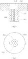
FIG. 2 is a schematic cross-sectional diagram showing a part of an insulation body in the reaction chamber according to the first embodiment of the present disclosure; -
FIG. 3 is a schematic top view showing the insulation body in the reaction chamber according to the first embodiment of the present disclosure; -
FIG. 4 is a schematic cross-sectional diagram showing a first insulation block in the reaction chamber according to the first embodiment of the present disclosure; -
FIG. 5 is a schematic top view showing the first insulation block in the reaction chamber according to the first embodiment of the present disclosure; -
FIG. 6 is a schematic cross-sectional diagram showing a second insulation block in the reaction chamber according to the first embodiment of the present disclosure; -
FIG. 7 is a schematic bottom view showing the second insulation block in the reaction chamber according to the first embodiment of the present disclosure; -
FIG. 8 is a schematic top view showing an insulation body in the reaction chamber according to a second embodiment of the present disclosure; and -
FIG. 9 is a schematic cross-sectional diagram showing the insulation body in the reaction chamber along line A-A inFIG. 8 according to the second embodiment of the present disclosure. -
- 100 Chamber body, 110 Inner chamber, 120 Heater;
- 200 Upper cover, 210 Through hole, 220 Uniform flow plate, 230 Showerhead;
- 300 Electrode;
- 400 Insulation member;
- 500 Insulation body, 510 First insulation block, 511 Accommodation space, 512 First gas inlet hole, 513 Body member, 514 Position limiting member, 520 Second insulation block, 521 Second gas inlet hole, 522a First groove, 522b Second groove, 530 Gas inlet pipe, 540 Flange part, 541 Third groove, 550 Convex member, D1 diameter of
first groove 522a, D2 diameter of inscribed circle formed by inner side edges of multiple gas inlet grooves; - 500' Insulation body, 501 Gas inlet channel, 501a First channel segment, 501b Second channel segment, 501c Third channel segment, 502a First connection channel, 502b Second connection channel, 503a First insulation block, 503b Second insulation block, 503c Third insulation block.
- In order to make the purposes, technical solutions, and advantages of the present disclosure clearer, the technical solutions of the present disclosure will be clearly and completely described below in connection with specific embodiments of the present disclosure and the corresponding accompanying drawings. Apparently, the described embodiments are only some embodiments of the present disclosure, not all the embodiments. All other embodiments obtained by those of ordinary skill in the art based on embodiments of the present disclosure without creative efforts shall be within the scope of the present disclosure.
- The technical solutions disclosed in various embodiments of the present disclosure are described in detail below in connection with the accompanying drawings.
- As shown in
FIG. 1 to FIG. 7 , the first embodiment of the present disclosure discloses a reaction chamber. The disclosed reaction chamber may be a metal-organic chemical vapor deposition (MOCVD) process chamber. The disclosed reaction chamber includes achamber body 100, anupper cover 200, and a gas inlet mechanism. - Referring to
FIG. 1 , thechamber body 100 is grounded. Theupper cover 200 is electrically connected to anelectrode 300. One end of theelectrode 300 may be arranged, e.g., on theupper cover 200, and the other end is electrically connected to a radio frequency source and configured to load radio frequency power output by the radio frequency source to theupper cover 200. Thechamber body 100 and theupper cover 200 are connected by aninsulation member 400. In the case that thechamber body 100 is connected to theupper cover 200, thechamber body 100 and theupper cover 200 form aninner chamber 110. A portion of theinner chamber 110 that corresponds to thechamber body 100 may be a first hollow chamber, and a portion that corresponds to theupper cover 200 may be a second hollow chamber, wherein aheater 120 is arranged in the first hollow chamber and configured to carry a substrate and heat the substrate. In a process of performing chemical vapor deposition, organic compounds of a group III element and a group II element and hydrides of a group V element and a group VI element may be used as crystal growth source materials, and vapor phase epitaxy may be performed at theheater 120 in a thermal decomposition reaction manner to grow various compound semiconductors of group III-V and group II-VI and thin layer single crystal material of a multi-element solid solution thereof. At the same time, in order to reduce resistivity of the material, theheater 120 is grounded through thechamber body 100. - Referring again to
FIG. 1 , auniform flow plate 220 and ashowerhead 230 are arranged in the second hollow chamber. Theuniform flow plate 220 is arranged opposite to theshowerhead 230, and theshowerhead 230 is arranged opposite to theheater 120. When the process is performed, the reaction gas first flows into the second hollow chamber. Theuniform flow plate 220 in the second hollow chamber body may be configured to uniform the reaction gas to cause the reaction gas flowing out of theuniform flow plate 220 to be relatively uniform. Thereafter, the reaction gas flowing out of theuniform flow plate 220 flows into theshowerhead 230. Theshowerhead 230 may be configured to spray the reaction gas flowing through to a surface of the substrate on theheater 120 to perform a vapor phase epitaxy reaction, so as to grow the required material on the surface of the substrate. In addition, theshowerhead 230 may be electrically connected to theupper cover 200. When theupper cover 200 is powered-on, theshowerhead 230 may be powered-on. A radio frequency electric field may be formed between the powered-onshowerhead 230 and the groundedheater 120. The radio frequency electric field may reduce the resistivity of the material grown on the surface of the substrate. - Correspondingly, a through-
hole 210 is arranged at theupper cover 200 in communication with theinner chamber 110. The gas inlet mechanism includes aninsulation body 500, which is at least partially arranged in the through-hole 210. A gas inlet channel may be arranged in theinsulation body 500, and a gas outlet end of the gas inlet channel may be communicated with theinner chamber 110. Aflange part 540 is arranged on a side of theinsulation body 500 facing away from theinner chamber 110. Theflange part 540 may be grounded and configured to communicate the gas inlet end of the gas inlet channel with a gas outlet end of agas inlet pipe 530 configured to transfer the reaction gas. Specifically, theflange part 540 is sealed and connected to thegas inlet pipe 530, so that the gas outlet end of thegas inlet pipe 530 may be communicated with the gas inlet end of the gas inlet channel. The other end of thegas inlet pipe 530 may be communicated with a container having the reaction gas. - The
insulation body 500 may have a plurality of structures. In embodiments of the present disclosure, theinsulation body 500 includes two insulation blocks arranged along an axis of the through-hole 210 in sequence, that is afirst insulation block 510 close to theinner chamber 110 and asecond insulation block 520 facing away from theinner chamber 110. At least a part of thefirst insulation block 510 may be located in the through-hole 210. As shown inFIG. 4 , one side of thefirst insulation block 510 facing away from theinner chamber 110 is provided with anaccommodation space 511, and thesecond insulation block 520 is arranged in theaccommodation space 511. As shown inFIG. 1 , theflange part 540 is arranged on a side surface of thefirst insulation block 510 facing away from theinner chamber 110 and blocks an opening of theaccommodation space 511. - The
second insulation block 520 is provided with a secondgas inlet hole 521. Thefirst insulation block 510 is provided with a firstgas inlet hole 512. A gas inlet end of the firstgas inlet hole 512 is communicated with a gas outlet end of the secondgas inlet hole 521. The gas outlet end of the firstgas inlet hole 512 is communicated with theinner chamber 110. Under this situation, the firstgas inlet hole 512 and the secondgas inlet hole 521 constitute two channel segments of the gas inlet channel, respectively. The reaction gas in thegas inlet pipe 530 may sequentially pass through the secondgas inlet hole 521 and the firstgas inlet hole 512 to flow into theinner chamber 110. In embodiments of the present disclosure, orthographic projections of the firstgas inlet hole 512 and the secondgas inlet hole 521 are staggered from each other on a plane perpendicular to an axial direction of the through-hole 210. That is, an axis of the firstgas inlet hole 512 is not in a straight line with an axis of the secondgas inlet hole 521. For example, the orthographic projection of the firstgas inlet hole 512 is outside the orthographic projection of the secondgas inlet hole 521. As such, when the upper cover is powered-on through the electrode, a radio frequency electric field is difficult to be formed between the grounded flange part and the upper cover and a powered-on part of the upper cover. Thus, occurrences of accidental discharge phenomenon may be reduced, a risk of generating the sparking phenomenon may be further reduced, and finally, the uniformity and stability of the surface material of the substrate may be improved. - In embodiments of the present disclosure, optionally, as shown in
FIG. 3 , a gas inlet groove is arranged at an outer peripheral surface of thesecond insulation block 520. The gas inlet groove ad an inner wall of theaccommodation space 511 may form the secondgas inlet hole 521. Compared with directly arranging the secondgas inlet hole 521 in thesecond insulation block 520, an arrangement of the gas inlet groove may be easier to process and form. Meanwhile, in this manner, the secondgas inlet hole 521 may be caused to be in an edge region of thesecond insulation block 520. Thus, the orthographic projection of the secondgas inlet hole 521 on the plane perpendicular to the axial direction of the through-hole 210 may be easier to be located outside the orthographic projection of the firstgas inlet hole 512 on the plane perpendicular to the axial direction of the through-hole 210. Thus, a staggered effect of the secondgas inlet hole 521 and the firstgas inlet hole 512 may be better. - In embodiments of the present disclosure, as shown in
FIG. 6 and FIG. 7 , afirst groove 522a is arranged on a side of thesecond insulation block 520 facing theinner chamber 110. Thefirst groove 522a and the inner wall of theaccommodation space 511 may form a first gas chamber. The firstgas inlet hole 512 may be communicated with the secondgas inlet hole 521 through the first gas chamber. When the process is performed, the reaction gas may first enter the first gas chamber via the secondgas inlet hole 521. The reaction gas that enters the first gas chamber may flow into theinner chamber 110 via the firstgas inlet hole 512. In such a manner, the firstgas inlet hole 512 may be facilitated to be communicated with the secondgas inlet hole 521, and other parts on a side of thesecond insulation block 520 facing theinner chamber 110 may be better supported in theaccommodation space 511, which facilitates the overall assembly. Of course, in practical applications, the communication between the firstgas inlet hole 512 and the secondgas inlet hole 521 may be realized by using any other structure. - In embodiments of the present disclosure, in an optional solution, as shown in
FIG. 7 , a plurality of second gas inlet holes 521 are included and are distributed along a circumferential direction of thefirst groove 522a at intervals. The plurality of second gas inlet holes 521 may be configured to increase a circulation rate of the reaction gas. Meanwhile, diameters of the plurality of second gas inlet holes 521 may be relatively small. Thus, the radio frequency electric field may be difficult to be generated between theflange part 540 and theupper cover 200 and a powered-on part of theupper cover 200, thereby better preventing generation of accidental discharge. - Moreover, the orthographic projection of an inner peripheral surface of the
first groove 522a on the plane perpendicular to the axial direction of the through-hole 210 may overlap with orthographic projections of the plurality of second gas inlet holes 521 on the plane perpendicular to the axial direction of the through-hole 210. For example, a plurality of gas inlet grooves may be arranged on the outer peripheral surface of thesecond insulation block 520 and distributed along a peripheral direction of thesecond insulation block 520 at intervals. The gas inlet grooves may form a plurality of second gas inlet holes 521 with the inner wall of theaccommodation space 511. Moreover, as shown inFIG. 7 , diameter D1 of thefirst groove 522a is larger than diameter D2 of an inscribed circle formed by inner side edges of the plurality of gas inlet grooves. Thus, thefirst groove 522a may be communicated with the gas inlet grooves. - In embodiments of the present disclosure, as shown in
FIG. 6 , a side of thesecond insulation block 520 facing away from theinner chamber 110 may be provided with asecond groove 522b. Thesecond groove 522b may form a second gas chamber with theflange part 540. The gas outlet end of thegas inlet pipe 530 may be communicated with the gas inlet end of the secondgas inlet hole 521 through the second gas chamber. When the process is performed, the reaction gas in thegas inlet pipe 530 may first enter the second gas chamber, and then enters the secondgas inlet hole 521 through the second gas chamber. In such a manner, thegas inlet pipe 530 may be facilitated to be communicated with the secondgas inlet hole 521. Under this situation, thegas inlet pipe 530 may not need to be directly connected to the secondgas inlet hole 521. Thus, assembly difficulty may be reduced. At the same time, when a plurality of second gas inlet holes 521 are included, the second gas chamber may enable the reaction gas flowing out from thegas inlet pipe 530 to flow into the second gas inlet holes 521. Thus, while the circulation rate of the reaction gas is increased, generation of an accidental discharge phenomenon may be prevented. - Optionally, as shown in
FIG. 1 , athird groove 541 is arranged on a side of theflange part 540 facing thesecond insulation block 520. Thethird groove 541 may be butted with thesecond groove 522b to form the second gas chamber to realize the communication between thegas inlet pipe 530 and the secondgas inlet hole 521. Of course, in practical applications, only thesecond groove 522b may be provided, or only thethird groove 541 may be provided. - Similarly, a plurality of first gas inlet holes 512 may be provided and arranged at the
first insulation block 510 at intervals. The plurality of first gas inlet holes 512 may enable the gas flowing out of the secondgas inlet hole 521 to flow quickly into theinner chamber 110. Similarly, diameters of the plurality of first gas inlet holes 512 may be relatively small. Thus, the radio frequency electric field may be difficult to be formed between theflange part 540 and theupper cover 200 and the powered-on part of theupper cover 200, and generation of accidental discharge may be better prevented. Optionally, under such a situation, the plurality of second gas inlet holes 521 may be provided at thesecond insulation block 520 at intervals. The plurality of second gas inlet holes 521 may be communicated with the plurality of first gas inlet holes 512 to increase the circulation rate of the reaction gas. - In embodiments of the present disclosure, the gas inlet mechanism may further include a position limiting structure. The position limiting structure may be arranged between the outer peripheral surface of the
second insulation block 520 and the inner wall of theaccommodation space 511 to limit rotation of thesecond insulation block 520 in theaccommodation space 511. For example, as shown inFIG. 2 , the position limiting structure includes aconvex member 550 arranged on the outer peripheral surface of thesecond insulation block 520 and a concave member arranged on the inner wall of theaccommodation space 511. Theconvex member 550 may cooperate with the concave member to prevent thesecond insulation block 520 from rotating in theaccommodation space 511. Optionally, theconvex member 550 may be an integral structure with thesecond insulation block 520. In this case, the inner wall of theaccommodation space 511 may be provided with a mounting groove, and at least a part of theconvex member 550 may be located in the mounting groove. - In embodiments of the present disclosure, the
first insulation block 510 may include abody member 513 and aposition limiting member 514. Thebody member 513 may be connected to theposition limiting member 514. Thebody member 513 may be arranged in the through-hole 210. Theposition limiting member 514 may be position-limited and cooperate with a side of the through-hole 210 facing away from theinner chamber 110. With such a manner, the connection between thefirst insulation block 510 and the through-hole 210 may be facilitated. At the same time, theposition limiting member 514 may not only have a position-limiting and cooperation function with the side of the through-hole 210 facing away from theinner chamber 110, but theposition limiting member 514 may also have a relatively large outer surface. Thus, theaccommodation space 511 may be facilitated to be arranged. - A difference of a reaction chamber provided by the second embodiment of the present disclosure, when the reaction chamber is compared to the reaction chamber of the first embodiment only includes that the structure of the insulation body is different. Specifically, referring to
FIG. 8 and FIG. 9 , in embodiments of the present disclosure, a gas inlet channel is arranged in the insulation body 500'. The insulation body 500' includes three insulation blocks sequentially arranged in a vertical direction (i.e., the same direction as the axial direction of the through-hole 210 inFIG. 1 ), which are afirst insulation block 503a, asecond insulation block 503b, and athird insulation block 503c arranged sequentially along a direction close to theinner chamber 110. The three insulation blocks may be sequentially stacked in the axial direction of the through-hole 210. A thirdgas inlet hole 501c may be arranged in thethird insulation block 503c, a secondgas inlet hole 501b may be arranged in thesecond insulation block 503b, and a firstgas inlet hole 501a may be arranged in thefirst insulation block 503a. The firstgas inlet hole 501a, the secondgas inlet hole 501b, and the thirdgas inlet hole 501c may constitute three channel segments of the gas inlet channel, respectively. - A gas outlet end of the third
gas inlet hole 501c may be communicated with theinner chamber 110, and a gas inlet end of the thirdgas inlet hole 501c may be communicated with a gas outlet end of the secondgas inlet hole 501b, for example, through asecond connection channel 502b arranged in the insulation body 500'. A gas inlet end of the secondgas inlet hole 501b may be communicated with a gas outlet end of the firstgas inlet hole 501a, for example, through afirst connection channel 502a arranged in the insulation body 500'. A gas inlet end of the firstgas inlet hole 501a may be communicated with a gas outlet end of the gas inlet pipe configured to transfer the reaction gas through the flange part. The flange part and the gas inlet pipe may adopt the same structure as theflange part 540 and thegas inlet pipe 530 shown inFIG. 1 . In this way, the reaction gas in thegas inlet pipe 530 may sequentially pass through the firstgas inlet hole 501a, the secondgas inlet hole 501b, and the thirdgas inlet hole 501c to flow into theinner chamber 110. - In embodiments of the present disclosure, as shown in
FIG. 8 , orthographic projections of the firstgas inlet hole 501a, the secondgas inlet hole 501b, and the thirdgas inlet hole 501c are staggered from each other on a plane perpendicular to the vertical direction. That is, any two axes of an axis of the firstgas inlet hole 501a, an axis of the secondgas inlet hole 501b, and an axis of the thirdgas inlet hole 501c are not in a straight line. For example, an orthographic projection of the secondgas inlet hole 501b is outside an orthographic projection of the thirdgas inlet hole 501c. An orthographic projection of the firstgas inlet hole 501a is located outside the orthographic projection of the secondgas inlet hole 501b. In this way, when the upper cover is powered-on through the electrode, a radio frequency electric field may be difficult to be formed between the grounded flange part and the upper cover and the powered-on part of the upper cover. Thus, occurrence of accidental discharge phenomenon may be reduced, a risk of generating the sparking phenomenon may be reduced, and finally, the uniformity and stability of the surface material of the substrate may be improved. - In embodiments of the present disclosure, as shown in
FIG. 9 , grooves are arranged on two opposite surfaces of thesecond insulation block 503b and thethird insulation block 503c, respectively. The two grooves may be butted to form thefirst connection channel 502a. Similarly, grooves are arranged on two opposite surfaces of thesecond insulation block 503b and thefirst insulation block 503a, respectively. The two grooves may be butted to form thesecond connection channel 502b. Of course, in practical applications, a groove may also be provided on one of the two opposite surfaces of thesecond insulation block 503b and thethird insulation block 503c, and thefirst connection channel 502a may also be formed. Moreover, a groove may be provided on one of the two opposite surfaces of thesecond insulation block 503b and thefirst insulation block 503a, and thesecond connection channel 502b may be also formed. In addition, in practical applications, the communication between the firstgas inlet hole 501a and the secondgas inlet hole 501b and the communication between the secondgas inlet hole 501b and the thirdgas inlet hole 501c may be realized in any other manners, which is not particularly limited in embodiments of the present disclosure. - In embodiments of the present disclosure, as shown in
FIG. 8 , optionally, a plurality of the firstgas inlet holes 501a are provided and arranged along a peripheral direction of the insulation body 500' at intervals. Similarly, a plurality of second gas inlet holes 501b are provided and arranged along the peripheral direction of the insulation body 500' at intervals. The plurality of second gas inlet holes 501b are located on an inner side of the plurality of firstgas inlet holes 501a. A plurality of third gas inlet holes 501c are provided and arranged on an inner side of the plurality of second gas inlet holes 501b. Thus, the circulation rate of the reaction gas may be increased. - It should be noted that, in embodiments of the present disclosure, the insulation body 500' includes the three insulation blocks stacked in sequence in the vertical direction (i.e., the same direction as the axial direction of the through-
hole 210 inFIG. 1 ). Thus, the gas inlet holes and corresponding grooves may be machined conveniently for the three insulation blocks, and eventually, the continuous gas inlet channel may be formed. Moreover, orthographic projections of any two adjacent channel segments of the gas inlet channel may be staggered from each other in the vertical direction. However, embodiments of the present disclosure are not limited to this. In practical applications, the insulation body may be divided into a plurality of partitions in any manner, as long as the gas inlet channel having the structure described above may be machined and obtained. Alternatively, the insulation body may also adopt an integrated structure. The gas inlet channel having the structure described above may be formed in the integrated insulation body by using an existing processing manner. For example, holes may be formed in different directions of the insulation body. The channel segments staggered with each other may be further machined through the opening holes, and the connection channel communicating the adjacent channel segments may be machined. Then, the opening holes may be blocked to obtain a closed gas inlet channel. - Other structures and functions not mentioned in the reaction chamber provided by the second embodiment of the present disclosure are not repeated here, since the other structures and functions are the same as the structures and functions in the first embodiment.
- It should be noted that, in practical applications, a number of insulation blocks included in the insulation body may also be four or more according to specific requirements. In addition, an arrangement manner between any two adjacent insulation blocks is not limited to the nesting manner in the above embodiments (that is, the upper insulation block is arranged in the accommodation space of the lower insulation block) and the stacking manner. In practical applications, the insulation blocks may be arranged in any other manners, for example, in a concentrically surrounding manner.
- In embodiments of the present disclosure, the differences between the embodiments are emphasized to be described. Different optimization features between the embodiments may be combined to form a better embodiment as long as there is no contradiction, which is not repeated here to keep the brevity of the text.
- The above are only embodiments of the present disclosure and are not intended to limit the present disclosure. For those skilled in the art, various modifications and variations may be made to the present disclosure. Any modifications, equivalent substitutions, and improvements made within the spirit and principle of the present application should be within the scope of the claims of the present application.
Claims (11)
- A reaction chamber comprising:a chamber body, the chamber body being grounded;an upper cover, the upper cover being electrically connected to an electrode, the chamber body being connected to the upper cover through an insulation member, the chamber body and the upper cover forming an inner chamber, and a through-hole communicating with the inner chamber being formed at the upper cover;a gas inlet mechanism, the gas inlet mechanism including an insulation body that is at least partially arranged in the through-hole, a gas inlet channel being arranged in the insulation body, a flange part being arranged on one side of the insulation body facing away from the inner chamber, the flange part being grounded and configured to communicate a gas inlet end of the gas inlet channel with a gas outlet end of a gas inlet pipe that is configured to transfer a reaction gas, a gas outlet end of the gas inlet channel being communicated with the inner chamber, the gas inlet channel including at least two channel segments communicated sequentially in an axial direction of the through-hole, and orthographic projections of any two adjacent channel segments on a plane perpendicular to the axial direction of the through-hole being staggered from each other.
- The reaction chamber according to claim 1, wherein the insulation body includes at least two insulation blocks arranged in sequence in the axial direction of the through-hole, and each insulation block is provided with a gas inlet hole used as a channel segment.
- The reaction chamber according to claim 2, wherein two insulation blocks are provided and include a first insulation block close to the inner chamber and a second insulation block facing away from the inner chamber, wherein the first insulation block is provided with a first gas inlet hole used as the channel segment, an accommodation space is formed on one side of the first insulation block facing away from the inner chamber, the second insulation block is arranged in the accommodation space, and the second insulation block is provided with a second gas inlet hole used as the channel segment.
- The reaction chamber according to claim 3, wherein a gas inlet groove is arranged on an outer peripheral surface of the second insulation block, and the gas inlet groove and an inner wall of the accommodation space form the second gas inlet hole.
- The reaction chamber according to claim 4, wherein a first groove is formed on a side of the second insulation block facing the inner chamber, the first groove and the inner wall of the accommodation space form a first gas chamber, and both the first gas inlet hole and the second gas inlet hole are communicated with the first gas chamber.
- The reaction chamber according to claim 5, wherein a plurality of second gas inlet holes are provided and distributed along a peripheral direction of the first groove at intervals, and an orthographic projection of an inner peripheral surface of the first groove on a plane perpendicular to an axial direction of the through-hole overlaps partially with orthographic projections of the second gas inlet holes on the plane perpendicular to the axial direction of the through-hole.
- The reaction chamber according to claim 3, wherein a plurality of first gas inlet holes are provided and arranged at the first insulation block at intervals.
- The reaction chamber according to claim 3, wherein a second groove is provided on a side of the second insulation block facing away from the inner chamber (110), the second groove and the flange part form a second gas chamber, and the second gas chamber is respectively communicated with the gas inlet end of the gas inlet channel and the gas outlet end of the gas inlet pipe.
- The reaction chamber according to claim 8, wherein a third groove is formed on a side of the flange part facing the second insulation block, and the third groove is butted with the second groove to form the second gas chamber.
- The reaction chamber according to claim 3, wherein the gas inlet mechanism further includes a position limiting structure, and the position limiting structure is arranged between an outer peripheral surface of the second insulation block and an inner wall of the accommodation space to limit rotation of the second insulation block in the accommodation space.
- The reaction chamber according to claim 1, wherein the reaction chamber is a metal-organic compound chemical vapor deposition process chamber.
Applications Claiming Priority (2)
| Application Number | Priority Date | Filing Date | Title |
|---|---|---|---|
| CN202010152523.3A CN111321463B (en) | 2020-03-06 | 2020-03-06 | Reaction chamber |
| PCT/CN2021/075520 WO2021175089A1 (en) | 2020-03-06 | 2021-02-05 | Reaction chamber |
Publications (3)
| Publication Number | Publication Date |
|---|---|
| EP4116467A1 true EP4116467A1 (en) | 2023-01-11 |
| EP4116467A4 EP4116467A4 (en) | 2024-04-03 |
| EP4116467B1 EP4116467B1 (en) | 2025-04-23 |
Family
ID=71169219
Family Applications (1)
| Application Number | Title | Priority Date | Filing Date |
|---|---|---|---|
| EP21764062.2A Active EP4116467B1 (en) | 2020-03-06 | 2021-02-05 | Reaction chamber |
Country Status (7)
| Country | Link |
|---|---|
| US (1) | US11773505B2 (en) |
| EP (1) | EP4116467B1 (en) |
| KR (1) | KR102527246B1 (en) |
| CN (1) | CN111321463B (en) |
| FI (1) | FI4116467T3 (en) |
| TW (1) | TWI794736B (en) |
| WO (1) | WO2021175089A1 (en) |
Families Citing this family (5)
| Publication number | Priority date | Publication date | Assignee | Title |
|---|---|---|---|---|
| CN111321463B (en) | 2020-03-06 | 2021-10-15 | 北京北方华创微电子装备有限公司 | Reaction chamber |
| CN114203511B (en) * | 2021-12-10 | 2024-04-12 | 北京北方华创微电子装备有限公司 | Upper electrode assembly and semiconductor process equipment |
| CN114517458B (en) * | 2022-02-23 | 2022-12-16 | 绿友集团新能源车辆有限公司 | Multi-functional electronic watering lorry |
| CN117427792A (en) * | 2022-07-14 | 2024-01-23 | 中微半导体设备(上海)股份有限公司 | Plasma processing equipment, gas shower head and manufacturing method thereof |
| CN118007105B (en) * | 2024-03-01 | 2025-02-18 | 纳设智能装备(江苏)有限公司 | Spraying assembly and spraying equipment |
Family Cites Families (42)
| Publication number | Priority date | Publication date | Assignee | Title |
|---|---|---|---|---|
| US6245192B1 (en) * | 1999-06-30 | 2001-06-12 | Lam Research Corporation | Gas distribution apparatus for semiconductor processing |
| KR100516844B1 (en) * | 2001-01-22 | 2005-09-26 | 동경 엘렉트론 주식회사 | Device and method for treatment |
| KR100756107B1 (en) * | 2001-02-09 | 2007-09-05 | 동경 엘렉트론 주식회사 | Deposition device |
| KR100400044B1 (en) * | 2001-07-16 | 2003-09-29 | 삼성전자주식회사 | Shower head of wafer treatment apparatus having gap controller |
| US6911391B2 (en) * | 2002-01-26 | 2005-06-28 | Applied Materials, Inc. | Integration of titanium and titanium nitride layers |
| JP4579157B2 (en) * | 2003-03-25 | 2010-11-10 | 東京エレクトロン株式会社 | Processing device and switching mechanism |
| US7712434B2 (en) * | 2004-04-30 | 2010-05-11 | Lam Research Corporation | Apparatus including showerhead electrode and heater for plasma processing |
| KR100852200B1 (en) * | 2004-06-03 | 2008-08-13 | 도쿄엘렉트론가부시키가이샤 | Plasma CVD devices |
| US20060162661A1 (en) * | 2005-01-22 | 2006-07-27 | Applied Materials, Inc. | Mixing energized and non-energized gases for silicon nitride deposition |
| KR100686724B1 (en) | 2005-06-30 | 2007-02-26 | 삼성전자주식회사 | Chemical Vapor Deposition Equipment |
| KR101019293B1 (en) * | 2005-11-04 | 2011-03-07 | 어플라이드 머티어리얼스, 인코포레이티드 | Plasma-Enhanced Atomic Layer Deposition Apparatus and Method |
| US20070187363A1 (en) * | 2006-02-13 | 2007-08-16 | Tokyo Electron Limited | Substrate processing apparatus and substrate processing method |
| KR100849929B1 (en) | 2006-09-16 | 2008-08-26 | 주식회사 피에조닉스 | Chemical vapor deposition method and apparatus equipped with a shower head for actively controlling the injection speed of the reaction gas |
| CN201071403Y (en) * | 2007-06-27 | 2008-06-11 | 江苏大学 | Upward-in and upward-out vertically spraying type MOCVD reactor |
| CN101314844B (en) * | 2008-06-20 | 2010-11-17 | 江苏大学 | A MOCVD reaction chamber with a horizontal tangential inlet and a central vertical outlet |
| CN100568453C (en) * | 2008-08-22 | 2009-12-09 | 北京北方微电子基地设备工艺研究中心有限责任公司 | Plasma processing apparatus, gas distribution device, and gas delivery method |
| CN101339895B (en) * | 2008-08-22 | 2010-06-02 | 北京北方微电子基地设备工艺研究中心有限责任公司 | Gas distribution device and plasma processing apparatus applying the same |
| JP2010161316A (en) * | 2009-01-09 | 2010-07-22 | Ulvac Japan Ltd | Plasma processing device |
| CN201626981U (en) * | 2009-09-02 | 2010-11-10 | 中国科学院半导体研究所 | Air intake device for chemical vapor deposition epitaxy equipment |
| CN201924077U (en) * | 2010-12-22 | 2011-08-10 | 北京京东方光电科技有限公司 | Chemical vapor deposition equipment and gas diffuser thereof |
| CN102352493A (en) * | 2011-11-16 | 2012-02-15 | 上海卓锐材料科技有限公司 | Device for realizing spray uniformity of MOCVD (Metal-Organic Chemical Vapor Deposition) and application of device |
| US9263240B2 (en) * | 2011-11-22 | 2016-02-16 | Lam Research Corporation | Dual zone temperature control of upper electrodes |
| CN102424956B (en) * | 2011-12-02 | 2013-07-10 | 彭继忠 | Spraying apparatus for metal-organic chemical vapor deposition equipment |
| CN102492937A (en) * | 2011-12-29 | 2012-06-13 | 中国科学院半导体研究所 | Inlet spray head used for reaction chamber of metal chemical vapor deposition equipment |
| JP5848140B2 (en) * | 2012-01-20 | 2016-01-27 | 東京エレクトロン株式会社 | Plasma processing equipment |
| TW201347035A (en) * | 2012-02-02 | 2013-11-16 | Greene Tweed Of Delaware | Gas dispersion plate for plasma reactor having extended lifetime |
| KR102061749B1 (en) | 2012-12-27 | 2020-01-02 | 주식회사 무한 | Apparatus for processing substrate |
| US9297489B2 (en) * | 2013-01-17 | 2016-03-29 | Canada Pipeline Accessories, Co. Ltd. | Extended length flow conditioner |
| JP6134522B2 (en) | 2013-01-30 | 2017-05-24 | 株式会社ニューフレアテクノロジー | Vapor growth apparatus and vapor growth method |
| CN104498904B (en) * | 2014-12-29 | 2017-04-26 | 华中科技大学 | Spray header for MOCVD equipment |
| KR102417934B1 (en) | 2015-07-07 | 2022-07-07 | 에이에스엠 아이피 홀딩 비.브이. | Thin Film Deposition Apparatus |
| CN205388967U (en) | 2015-08-25 | 2016-07-20 | 沈阳拓荆科技有限公司 | Device for preventing strike sparks in semiconductor coating equipment "The reaction chamber" |
| CN107180782B (en) | 2016-03-09 | 2021-01-08 | 北京北方华创微电子装备有限公司 | A susceptor and reaction chamber |
| CN108293292B (en) * | 2016-03-30 | 2020-08-18 | 东京毅力科创株式会社 | Plasma electrode and plasma processing apparatus |
| CN106011792B (en) * | 2016-07-26 | 2019-01-29 | 北京中科优唯科技有限公司 | The even pneumatic module of MOCVD upper lower burrs of rotary premixed gas |
| CN108538694B (en) | 2017-03-02 | 2020-04-28 | 北京北方华创微电子装备有限公司 | Chamber and plasma processing device |
| CN108573891B (en) | 2017-03-07 | 2022-01-11 | 北京北方华创微电子装备有限公司 | Plasma processing apparatus |
| US10649006B2 (en) * | 2017-10-06 | 2020-05-12 | Lam Research Corporation | Cathode RF asymmetry detection probe for semiconductor RF plasma processing equipment |
| CN109487238B (en) * | 2018-12-17 | 2021-01-29 | 北京北方华创微电子装备有限公司 | Air inlet grid assembly and atomic layer deposition equipment |
| CN110172682A (en) * | 2019-04-30 | 2019-08-27 | 中国科学院半导体研究所 | The inlet spray head of vapor deposition apparatus |
| CN111321463B (en) | 2020-03-06 | 2021-10-15 | 北京北方华创微电子装备有限公司 | Reaction chamber |
| KR20220021206A (en) * | 2020-08-13 | 2022-02-22 | 삼성전자주식회사 | Plasma processing apparatus |
-
2020
- 2020-03-06 CN CN202010152523.3A patent/CN111321463B/en active Active
-
2021
- 2021-02-05 US US17/802,843 patent/US11773505B2/en active Active
- 2021-02-05 WO PCT/CN2021/075520 patent/WO2021175089A1/en not_active Ceased
- 2021-02-05 KR KR1020227029506A patent/KR102527246B1/en active Active
- 2021-02-05 EP EP21764062.2A patent/EP4116467B1/en active Active
- 2021-02-05 FI FIEP21764062.2T patent/FI4116467T3/en active
- 2021-02-08 TW TW110104674A patent/TWI794736B/en active
Also Published As
| Publication number | Publication date |
|---|---|
| KR20220129633A (en) | 2022-09-23 |
| TW202134470A (en) | 2021-09-16 |
| WO2021175089A1 (en) | 2021-09-10 |
| EP4116467B1 (en) | 2025-04-23 |
| TWI794736B (en) | 2023-03-01 |
| US20230028116A1 (en) | 2023-01-26 |
| KR102527246B1 (en) | 2023-04-28 |
| FI4116467T3 (en) | 2025-06-04 |
| US11773505B2 (en) | 2023-10-03 |
| CN111321463A (en) | 2020-06-23 |
| EP4116467A4 (en) | 2024-04-03 |
| CN111321463B (en) | 2021-10-15 |
Similar Documents
| Publication | Publication Date | Title |
|---|---|---|
| EP4116467B1 (en) | Reaction chamber | |
| US10822695B2 (en) | Thin film deposition apparatus | |
| US10358721B2 (en) | Semiconductor manufacturing system including deposition apparatus | |
| US10593560B2 (en) | Magnetic induction plasma source for semiconductor processes and equipment | |
| US12237182B2 (en) | Showerhead device for semiconductor processing system | |
| TWI496928B (en) | Film evaporation device | |
| KR20050041582A (en) | Chemical vapor deposition unit | |
| US20090159432A1 (en) | Thin-film deposition apparatus using discharge electrode and solar cell fabrication method | |
| JP2007227375A (en) | Long-distance plasma generator | |
| US20050092245A1 (en) | Plasma chemical vapor deposition apparatus having an improved nozzle configuration | |
| US20230402265A1 (en) | Process chamber and semiconductor process device | |
| US20070163501A1 (en) | Plasma processing apparatus | |
| KR20250056972A (en) | Spray plate, spray method and treatment device | |
| JP2025081293A (en) | Semiconductor Processing Chamber Adapter | |
| US11804363B2 (en) | Chamber components for gas delivery modulation | |
| CN109487238B (en) | Air inlet grid assembly and atomic layer deposition equipment | |
| US20230187181A1 (en) | Plasma-enhanced thin-film-deposition equipment | |
| WO2023093351A1 (en) | Film-forming device | |
| CN117987806A (en) | Gas distribution component, gas delivery device and film processing device | |
| US20250037976A1 (en) | Process stack for cvd plasma treatment | |
| US20060112877A1 (en) | Nozzle and plasma apparatus incorporating the nozzle | |
| CN120193256A (en) | Inner cavity of atomic layer deposition device and dual-chamber atomic layer deposition device | |
| CN117385452A (en) | Plasma starting chamber, radio frequency plasma device and molecular beam epitaxy equipment | |
| JPH01180982A (en) | Plasma cvd device | |
| CN121428535A (en) | A remote and local dual-source plasma-assisted chemical vapor deposition coating device |
Legal Events
| Date | Code | Title | Description |
|---|---|---|---|
| STAA | Information on the status of an ep patent application or granted ep patent |
Free format text: STATUS: THE INTERNATIONAL PUBLICATION HAS BEEN MADE |
|
| PUAI | Public reference made under article 153(3) epc to a published international application that has entered the european phase |
Free format text: ORIGINAL CODE: 0009012 |
|
| STAA | Information on the status of an ep patent application or granted ep patent |
Free format text: STATUS: REQUEST FOR EXAMINATION WAS MADE |
|
| 17P | Request for examination filed |
Effective date: 20220826 |
|
| AK | Designated contracting states |
Kind code of ref document: A1 Designated state(s): AL AT BE BG CH CY CZ DE DK EE ES FI FR GB GR HR HU IE IS IT LI LT LU LV MC MK MT NL NO PL PT RO RS SE SI SK SM TR |
|
| DAV | Request for validation of the european patent (deleted) | ||
| DAX | Request for extension of the european patent (deleted) | ||
| REG | Reference to a national code |
Ref legal event code: R079 Ref country code: DE Ref document number: 602021029651 Country of ref document: DE Free format text: PREVIOUS MAIN CLASS: C30B0025080000 Ipc: C23C0016455000 |
|
| A4 | Supplementary search report drawn up and despatched |
Effective date: 20240304 |
|
| RIC1 | Information provided on ipc code assigned before grant |
Ipc: C30B 30/02 20060101ALI20240227BHEP Ipc: C30B 25/14 20060101ALI20240227BHEP Ipc: C30B 25/08 20060101ALI20240227BHEP Ipc: H01J 37/32 20060101ALI20240227BHEP Ipc: C23C 16/509 20060101ALI20240227BHEP Ipc: C23C 16/455 20060101AFI20240227BHEP |
|
| GRAP | Despatch of communication of intention to grant a patent |
Free format text: ORIGINAL CODE: EPIDOSNIGR1 |
|
| STAA | Information on the status of an ep patent application or granted ep patent |
Free format text: STATUS: GRANT OF PATENT IS INTENDED |
|
| INTG | Intention to grant announced |
Effective date: 20241112 |
|
| GRAJ | Information related to disapproval of communication of intention to grant by the applicant or resumption of examination proceedings by the epo deleted |
Free format text: ORIGINAL CODE: EPIDOSDIGR1 |
|
| STAA | Information on the status of an ep patent application or granted ep patent |
Free format text: STATUS: REQUEST FOR EXAMINATION WAS MADE |
|
| P01 | Opt-out of the competence of the unified patent court (upc) registered |
Free format text: CASE NUMBER: APP_66683/2024 Effective date: 20241217 |
|
| GRAP | Despatch of communication of intention to grant a patent |
Free format text: ORIGINAL CODE: EPIDOSNIGR1 |
|
| STAA | Information on the status of an ep patent application or granted ep patent |
Free format text: STATUS: GRANT OF PATENT IS INTENDED |
|
| INTC | Intention to grant announced (deleted) | ||
| INTG | Intention to grant announced |
Effective date: 20250131 |
|
| GRAS | Grant fee paid |
Free format text: ORIGINAL CODE: EPIDOSNIGR3 |
|
| GRAA | (expected) grant |
Free format text: ORIGINAL CODE: 0009210 |
|
| STAA | Information on the status of an ep patent application or granted ep patent |
Free format text: STATUS: THE PATENT HAS BEEN GRANTED |
|
| AK | Designated contracting states |
Kind code of ref document: B1 Designated state(s): AL AT BE BG CH CY CZ DE DK EE ES FI FR GB GR HR HU IE IS IT LI LT LU LV MC MK MT NL NO PL PT RO RS SE SI SK SM TR |
|
| REG | Reference to a national code |
Ref country code: GB Ref legal event code: FG4D |
|
| REG | Reference to a national code |
Ref country code: CH Ref legal event code: EP |
|
| REG | Reference to a national code |
Ref country code: DE Ref legal event code: R096 Ref document number: 602021029651 Country of ref document: DE |
|
| REG | Reference to a national code |
Ref country code: IE Ref legal event code: FG4D |
|
| REG | Reference to a national code |
Ref country code: NL Ref legal event code: FP Ref country code: FI Ref legal event code: FGE |
|
| REG | Reference to a national code |
Ref country code: AT Ref legal event code: MK05 Ref document number: 1787825 Country of ref document: AT Kind code of ref document: T Effective date: 20250423 |
|
| PG25 | Lapsed in a contracting state [announced via postgrant information from national office to epo] |
Ref country code: ES Free format text: LAPSE BECAUSE OF FAILURE TO SUBMIT A TRANSLATION OF THE DESCRIPTION OR TO PAY THE FEE WITHIN THE PRESCRIBED TIME-LIMIT Effective date: 20250423 Ref country code: PT Free format text: LAPSE BECAUSE OF FAILURE TO SUBMIT A TRANSLATION OF THE DESCRIPTION OR TO PAY THE FEE WITHIN THE PRESCRIBED TIME-LIMIT Effective date: 20250825 |
|
| REG | Reference to a national code |
Ref country code: LT Ref legal event code: MG9D |
|
| PG25 | Lapsed in a contracting state [announced via postgrant information from national office to epo] |
Ref country code: GR Free format text: LAPSE BECAUSE OF FAILURE TO SUBMIT A TRANSLATION OF THE DESCRIPTION OR TO PAY THE FEE WITHIN THE PRESCRIBED TIME-LIMIT Effective date: 20250724 Ref country code: NO Free format text: LAPSE BECAUSE OF FAILURE TO SUBMIT A TRANSLATION OF THE DESCRIPTION OR TO PAY THE FEE WITHIN THE PRESCRIBED TIME-LIMIT Effective date: 20250723 |
|
| PG25 | Lapsed in a contracting state [announced via postgrant information from national office to epo] |
Ref country code: PL Free format text: LAPSE BECAUSE OF FAILURE TO SUBMIT A TRANSLATION OF THE DESCRIPTION OR TO PAY THE FEE WITHIN THE PRESCRIBED TIME-LIMIT Effective date: 20250423 |
|
| PG25 | Lapsed in a contracting state [announced via postgrant information from national office to epo] |
Ref country code: BG Free format text: LAPSE BECAUSE OF FAILURE TO SUBMIT A TRANSLATION OF THE DESCRIPTION OR TO PAY THE FEE WITHIN THE PRESCRIBED TIME-LIMIT Effective date: 20250423 |
|
| PG25 | Lapsed in a contracting state [announced via postgrant information from national office to epo] |
Ref country code: HR Free format text: LAPSE BECAUSE OF FAILURE TO SUBMIT A TRANSLATION OF THE DESCRIPTION OR TO PAY THE FEE WITHIN THE PRESCRIBED TIME-LIMIT Effective date: 20250423 |
|
| PG25 | Lapsed in a contracting state [announced via postgrant information from national office to epo] |
Ref country code: AT Free format text: LAPSE BECAUSE OF FAILURE TO SUBMIT A TRANSLATION OF THE DESCRIPTION OR TO PAY THE FEE WITHIN THE PRESCRIBED TIME-LIMIT Effective date: 20250423 |
|
| PG25 | Lapsed in a contracting state [announced via postgrant information from national office to epo] |
Ref country code: RS Free format text: LAPSE BECAUSE OF FAILURE TO SUBMIT A TRANSLATION OF THE DESCRIPTION OR TO PAY THE FEE WITHIN THE PRESCRIBED TIME-LIMIT Effective date: 20250723 |
|
| PG25 | Lapsed in a contracting state [announced via postgrant information from national office to epo] |
Ref country code: IS Free format text: LAPSE BECAUSE OF FAILURE TO SUBMIT A TRANSLATION OF THE DESCRIPTION OR TO PAY THE FEE WITHIN THE PRESCRIBED TIME-LIMIT Effective date: 20250823 |
|
| PG25 | Lapsed in a contracting state [announced via postgrant information from national office to epo] |
Ref country code: LV Free format text: LAPSE BECAUSE OF FAILURE TO SUBMIT A TRANSLATION OF THE DESCRIPTION OR TO PAY THE FEE WITHIN THE PRESCRIBED TIME-LIMIT Effective date: 20250423 |
|
| PG25 | Lapsed in a contracting state [announced via postgrant information from national office to epo] |
Ref country code: DK Free format text: LAPSE BECAUSE OF FAILURE TO SUBMIT A TRANSLATION OF THE DESCRIPTION OR TO PAY THE FEE WITHIN THE PRESCRIBED TIME-LIMIT Effective date: 20250423 Ref country code: SM Free format text: LAPSE BECAUSE OF FAILURE TO SUBMIT A TRANSLATION OF THE DESCRIPTION OR TO PAY THE FEE WITHIN THE PRESCRIBED TIME-LIMIT Effective date: 20250423 |
|
| PG25 | Lapsed in a contracting state [announced via postgrant information from national office to epo] |
Ref country code: CZ Free format text: LAPSE BECAUSE OF FAILURE TO SUBMIT A TRANSLATION OF THE DESCRIPTION OR TO PAY THE FEE WITHIN THE PRESCRIBED TIME-LIMIT Effective date: 20250423 |
|
| PG25 | Lapsed in a contracting state [announced via postgrant information from national office to epo] |
Ref country code: EE Free format text: LAPSE BECAUSE OF FAILURE TO SUBMIT A TRANSLATION OF THE DESCRIPTION OR TO PAY THE FEE WITHIN THE PRESCRIBED TIME-LIMIT Effective date: 20250423 |
|
| REG | Reference to a national code |
Ref country code: DE Ref legal event code: R097 Ref document number: 602021029651 Country of ref document: DE |
|
| PG25 | Lapsed in a contracting state [announced via postgrant information from national office to epo] |
Ref country code: SK Free format text: LAPSE BECAUSE OF FAILURE TO SUBMIT A TRANSLATION OF THE DESCRIPTION OR TO PAY THE FEE WITHIN THE PRESCRIBED TIME-LIMIT Effective date: 20250423 |
|
| PLBE | No opposition filed within time limit |
Free format text: ORIGINAL CODE: 0009261 |
|
| STAA | Information on the status of an ep patent application or granted ep patent |
Free format text: STATUS: NO OPPOSITION FILED WITHIN TIME LIMIT |
|
| REG | Reference to a national code |
Ref country code: CH Ref legal event code: L10 Free format text: ST27 STATUS EVENT CODE: U-0-0-L10-L00 (AS PROVIDED BY THE NATIONAL OFFICE) Effective date: 20260304 |
|
| PGFP | Annual fee paid to national office [announced via postgrant information from national office to epo] |
Ref country code: NL Payment date: 20260202 Year of fee payment: 6 |
|
| 26N | No opposition filed |
Effective date: 20260126 |
|
| PGFP | Annual fee paid to national office [announced via postgrant information from national office to epo] |
Ref country code: GB Payment date: 20260203 Year of fee payment: 6 |
|
| PGFP | Annual fee paid to national office [announced via postgrant information from national office to epo] |
Ref country code: DE Payment date: 20260217 Year of fee payment: 6 |
|
| PGFP | Annual fee paid to national office [announced via postgrant information from national office to epo] |
Ref country code: BE Payment date: 20260209 Year of fee payment: 6 Ref country code: FI Payment date: 20260217 Year of fee payment: 6 Ref country code: IT Payment date: 20260227 Year of fee payment: 6 |
|
| PGFP | Annual fee paid to national office [announced via postgrant information from national office to epo] |
Ref country code: FR Payment date: 20260202 Year of fee payment: 6 |