EP4113589A2 - Header for semiconductor package, and semiconductor package - Google Patents
Header for semiconductor package, and semiconductor package Download PDFInfo
- Publication number
- EP4113589A2 EP4113589A2 EP22179286.4A EP22179286A EP4113589A2 EP 4113589 A2 EP4113589 A2 EP 4113589A2 EP 22179286 A EP22179286 A EP 22179286A EP 4113589 A2 EP4113589 A2 EP 4113589A2
- Authority
- EP
- European Patent Office
- Prior art keywords
- lead
- hole
- semiconductor package
- insulating substrate
- conductive layer
- Prior art date
- Legal status (The legal status is an assumption and is not a legal conclusion. Google has not performed a legal analysis and makes no representation as to the accuracy of the status listed.)
- Pending
Links
Images






Classifications
-
- H—ELECTRICITY
- H01—ELECTRIC ELEMENTS
- H01S—DEVICES USING THE PROCESS OF LIGHT AMPLIFICATION BY STIMULATED EMISSION OF RADIATION [LASER] TO AMPLIFY OR GENERATE LIGHT; DEVICES USING STIMULATED EMISSION OF ELECTROMAGNETIC RADIATION IN WAVE RANGES OTHER THAN OPTICAL
- H01S5/00—Semiconductor lasers
- H01S5/02—Structural details or components not essential to laser action
- H01S5/022—Mountings; Housings
- H01S5/0233—Mounting configuration of laser chips
- H01S5/02345—Wire-bonding
-
- H—ELECTRICITY
- H01—ELECTRIC ELEMENTS
- H01S—DEVICES USING THE PROCESS OF LIGHT AMPLIFICATION BY STIMULATED EMISSION OF RADIATION [LASER] TO AMPLIFY OR GENERATE LIGHT; DEVICES USING STIMULATED EMISSION OF ELECTROMAGNETIC RADIATION IN WAVE RANGES OTHER THAN OPTICAL
- H01S5/00—Semiconductor lasers
- H01S5/02—Structural details or components not essential to laser action
- H01S5/022—Mountings; Housings
- H01S5/023—Mount members, e.g. sub-mount members
- H01S5/02315—Support members, e.g. bases or carriers
-
- H—ELECTRICITY
- H10—SEMICONDUCTOR DEVICES; ELECTRIC SOLID-STATE DEVICES NOT OTHERWISE PROVIDED FOR
- H10H—INORGANIC LIGHT-EMITTING SEMICONDUCTOR DEVICES HAVING POTENTIAL BARRIERS
- H10H20/00—Individual inorganic light-emitting semiconductor devices having potential barriers, e.g. light-emitting diodes [LED]
- H10H20/80—Constructional details
- H10H20/85—Packages
- H10H20/858—Means for heat extraction or cooling
- H10H20/8585—Means for heat extraction or cooling being an interconnection
-
- H—ELECTRICITY
- H01—ELECTRIC ELEMENTS
- H01S—DEVICES USING THE PROCESS OF LIGHT AMPLIFICATION BY STIMULATED EMISSION OF RADIATION [LASER] TO AMPLIFY OR GENERATE LIGHT; DEVICES USING STIMULATED EMISSION OF ELECTROMAGNETIC RADIATION IN WAVE RANGES OTHER THAN OPTICAL
- H01S5/00—Semiconductor lasers
- H01S5/02—Structural details or components not essential to laser action
- H01S5/022—Mountings; Housings
- H01S5/023—Mount members, e.g. sub-mount members
- H01S5/0232—Lead-frames
-
- H—ELECTRICITY
- H01—ELECTRIC ELEMENTS
- H01S—DEVICES USING THE PROCESS OF LIGHT AMPLIFICATION BY STIMULATED EMISSION OF RADIATION [LASER] TO AMPLIFY OR GENERATE LIGHT; DEVICES USING STIMULATED EMISSION OF ELECTROMAGNETIC RADIATION IN WAVE RANGES OTHER THAN OPTICAL
- H01S5/00—Semiconductor lasers
- H01S5/02—Structural details or components not essential to laser action
- H01S5/024—Arrangements for thermal management
- H01S5/02461—Structure or details of the laser chip to manipulate the heat flow, e.g. passive layers in the chip with a low heat conductivity
-
- H—ELECTRICITY
- H10—SEMICONDUCTOR DEVICES; ELECTRIC SOLID-STATE DEVICES NOT OTHERWISE PROVIDED FOR
- H10H—INORGANIC LIGHT-EMITTING SEMICONDUCTOR DEVICES HAVING POTENTIAL BARRIERS
- H10H20/00—Individual inorganic light-emitting semiconductor devices having potential barriers, e.g. light-emitting diodes [LED]
- H10H20/80—Constructional details
- H10H20/85—Packages
- H10H20/857—Interconnections, e.g. lead-frames, bond wires or solder balls
-
- H—ELECTRICITY
- H10—SEMICONDUCTOR DEVICES; ELECTRIC SOLID-STATE DEVICES NOT OTHERWISE PROVIDED FOR
- H10W—GENERIC PACKAGES, INTERCONNECTIONS, CONNECTORS OR OTHER CONSTRUCTIONAL DETAILS OF DEVICES COVERED BY CLASS H10
- H10W40/00—Arrangements for thermal protection or thermal control
- H10W40/20—Arrangements for cooling
- H10W40/28—Arrangements for cooling comprising Peltier coolers
-
- H—ELECTRICITY
- H10—SEMICONDUCTOR DEVICES; ELECTRIC SOLID-STATE DEVICES NOT OTHERWISE PROVIDED FOR
- H10W—GENERIC PACKAGES, INTERCONNECTIONS, CONNECTORS OR OTHER CONSTRUCTIONAL DETAILS OF DEVICES COVERED BY CLASS H10
- H10W70/00—Package substrates; Interposers; Redistribution layers [RDL]
- H10W70/60—Insulating or insulated package substrates; Interposers; Redistribution layers
-
- H—ELECTRICITY
- H10—SEMICONDUCTOR DEVICES; ELECTRIC SOLID-STATE DEVICES NOT OTHERWISE PROVIDED FOR
- H10W—GENERIC PACKAGES, INTERCONNECTIONS, CONNECTORS OR OTHER CONSTRUCTIONAL DETAILS OF DEVICES COVERED BY CLASS H10
- H10W70/00—Package substrates; Interposers; Redistribution layers [RDL]
- H10W70/60—Insulating or insulated package substrates; Interposers; Redistribution layers
- H10W70/62—Insulating or insulated package substrates; Interposers; Redistribution layers characterised by their interconnections
- H10W70/63—Vias, e.g. via plugs
- H10W70/635—Through-vias
-
- H—ELECTRICITY
- H10—SEMICONDUCTOR DEVICES; ELECTRIC SOLID-STATE DEVICES NOT OTHERWISE PROVIDED FOR
- H10W—GENERIC PACKAGES, INTERCONNECTIONS, CONNECTORS OR OTHER CONSTRUCTIONAL DETAILS OF DEVICES COVERED BY CLASS H10
- H10W70/00—Package substrates; Interposers; Redistribution layers [RDL]
- H10W70/60—Insulating or insulated package substrates; Interposers; Redistribution layers
- H10W70/62—Insulating or insulated package substrates; Interposers; Redistribution layers characterised by their interconnections
- H10W70/65—Shapes or dispositions of interconnections
-
- H—ELECTRICITY
- H10—SEMICONDUCTOR DEVICES; ELECTRIC SOLID-STATE DEVICES NOT OTHERWISE PROVIDED FOR
- H10W—GENERIC PACKAGES, INTERCONNECTIONS, CONNECTORS OR OTHER CONSTRUCTIONAL DETAILS OF DEVICES COVERED BY CLASS H10
- H10W76/00—Containers; Fillings or auxiliary members therefor; Seals
- H10W76/10—Containers or parts thereof
- H10W76/12—Containers or parts thereof characterised by their shape
- H10W76/13—Containers comprising a conductive base serving as an interconnection
- H10W76/132—Containers comprising a conductive base serving as an interconnection having other interconnections through an insulated passage in the conductive base
-
- H—ELECTRICITY
- H01—ELECTRIC ELEMENTS
- H01S—DEVICES USING THE PROCESS OF LIGHT AMPLIFICATION BY STIMULATED EMISSION OF RADIATION [LASER] TO AMPLIFY OR GENERATE LIGHT; DEVICES USING STIMULATED EMISSION OF ELECTROMAGNETIC RADIATION IN WAVE RANGES OTHER THAN OPTICAL
- H01S5/00—Semiconductor lasers
- H01S5/02—Structural details or components not essential to laser action
- H01S5/022—Mountings; Housings
- H01S5/02208—Mountings; Housings characterised by the shape of the housings
- H01S5/02212—Can-type, e.g. TO-CAN housings with emission along or parallel to symmetry axis
-
- H—ELECTRICITY
- H01—ELECTRIC ELEMENTS
- H01S—DEVICES USING THE PROCESS OF LIGHT AMPLIFICATION BY STIMULATED EMISSION OF RADIATION [LASER] TO AMPLIFY OR GENERATE LIGHT; DEVICES USING STIMULATED EMISSION OF ELECTROMAGNETIC RADIATION IN WAVE RANGES OTHER THAN OPTICAL
- H01S5/00—Semiconductor lasers
- H01S5/02—Structural details or components not essential to laser action
- H01S5/022—Mountings; Housings
- H01S5/023—Mount members, e.g. sub-mount members
- H01S5/0231—Stems
Definitions
- the present invention relates to headers for semiconductor packages, and semiconductor packages.
- the header may sometimes also be referred to as a stem.
- a cooling element for temperature adjustment is provided in a case where an amount of heat generated from the light emitting element is large.
- the light emitting element may be provided on a device mounting insulating substrate disposed on the cooling element.
- a transmission line length from a signal lead to the light emitting element becomes long because the cooling element is relatively thick, and a predetermined characteristic impedance may not be obtainable in some cases.
- considerations need to be taken so that the heat of the light emitting element, transferred by the provision of the cooling element, will not be returned toward the light emitting element.
- a header for a semiconductor package having a configuration that takes into consideration the characteristic impedance and cooling performance of the semiconductor package.
- a header for a semiconductor package includes an eyelet having a through hole penetrating the eyelet from an upper surface to a lower surface of the eyelet; a first lead inserted inside the through hole; and an insulating substrate disposed on the upper surface of the eyelet, and provided with a first through hole at a position overlapping one end of the first lead in a plan view, wherein the insulating substrate has a thermal conductivity lower than a thermal conductivity of the first lead, a first conductive layer is formed on an inner wall defining the first through hole, and the first conductive layer extends to an upper surface of the insulating substrate, the one end of the first lead is electrically connected to the first conductive layer, and a space is provided above the one end of the first lead inside the first through hole.
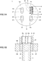
- FIG. 1A and FIG. 1B are diagrams illustrating an example of a header for a semiconductor package according to a first embodiment.
- FIG. 1A is a plan view of the header
- FIG. 1B is a partial cross sectional view of the header along a line A-A in FIG. 1A .
- a header 1 for a semiconductor package (hereinafter also referred to as a semiconductor package header 1) according to the first embodiment includes an eyelet 10, a first lead 21, a second lead 22, a third lead 23, a fourth lead 24, a fifth lead 25, a sixth lead 26, a seventh lead 27, an eighth lead 28, a seal 30, and an insulating substrate 40.
- the semiconductor package header 1 can be used as a header for optical communication, for example.
- each of the first through eighth leads 21 through 28 may simply be referred to as a lead.
- the eyelet 10 is a disk shaped member.
- a diameter of the eyelet 10 is not particularly limited, and can be appropriately determined according to purpose thereof, and can be 3.8 mm, 5.6 mm, or the like, for example.
- a thickness of the eyelet 10 is not particularly limited, and can be appropriately determined according to purpose thereof, and can be in a range of approximately 1.0 mm to approximately 1.5 mm, for example.
- the eyelet 10 can be formed of a metallic material, such as iron or the like, for example.
- the eyelet 10 can be formed of a metallic material (for example, a so-called cladding material) in which a plurality of metal layers (for example, copper layers, iron layers, or the like) are laminated.
- a gold plating or the like can be provided on a surface of the eyelet 10.
- the term "disk shaped member” refers to a member having a planar shape that is approximately circular and having a predetermined thickness.
- the thickness relative to the diameter of the disk shaped member is not particularly limited, and can be small or large.
- the disk shaped member can include a concave portion, a convex portion, a through hole, or the like formed in a portion thereof.
- a plan view of an object refers to a view of the object in a normal direction to an upper surface 10a of the eyelet 10
- a planar shape of the object refers to a shape of the object in the plan view viewed in the normal direction to the upper surface 10a of the eyelet 10.
- One or more cutouts having a shape recessed from an outer periphery towards a center of the eyelet 10 in the plan view, can be formed at an outer edge of the eyelet 10.
- the cutout can be a recess having a planar shape that is generally triangular or generally rectangular, for example.
- the cutout can be used for positioning or the like of a device mounting surface when mounting a semiconductor device on the semiconductor package header 1, for example.
- the cutout can be used for positioning or the like of a rotating direction of the semiconductor package header 1, for example.
- Each lead is inserted into a through hole 10x that penetrates the eyelet 10 from the upper surface 10a to a lower surface 10b thereof, in a state where a longitudinal direction of each lead penetrates a thickness direction of the eyelet 10, and a periphery of each lead is sealed by the seal 30.
- the seal 30 is made of an insulating material, such as glass or the like, for example.
- the glass can be soft glass, typified by soft glass having a relative dielectric constant of approximately 6.7, for example.
- a single lead can be disposed inside one through hole 10x, or multiple leads can be disposed inside one through hole 10x. In the example illustrated in FIG. 1A and FIG. 1B , two leads are disposed inside one through hole 10x.
- a protruding amount of each of the first lead 21 and the second lead 22 can be in a range of approximately 0.1 mm to approximately 0.3 mm, for example.
- Leads other than the first lead 21 and the second lead 22 can also protrude upward from the upper surface 10a of the eyelet 10, as required.
- Each lead protrudes downward from the lower surface 10b of the eyelet 10.
- a protruding amount of each lead from the lower surface 10b of the eyelet 10 can be in a range of approximately 6 mm to approximately 10 mm, for example.
- Each lead can be formed of a metal, such as iron nickel alloy, kovar, or the like, for example, and a gold plating or the like can be provided on a surface of each lead.
- the first lead 21 and the second lead 22 are disposed adjacent to each other, and provide a path for differential signaling electrically connected to a light emitting element, when mounting the light emitting element on the semiconductor package header 1 for use as the semiconductor package.
- the leads other than the first lead 21 and the second lead 22 provide a path for a ground GND, a signal path electrically connected to a cooling element mounted on the semiconductor package header 1, a signal path electrically connected to a temperature sensor mounted on the semiconductor package header 1, or the like, for example.
- the number of leads is not particularly limited, and can be increased or decreased, as required.
- the insulating substrate 40 is disposed on the upper surface 10a of the eyelet 10.
- the insulating substrate 40 is bonded to the upper surface 10a of the eyelet 10 using gold tin (AnSn) solder, silver paste, or the like, for example.
- the insulating substrate 40 is formed of a material having a thermal conductivity lower than a thermal conductivity of a material forming each lead. More particularly, a glass substrate is preferably used as the insulating substrate 40. Examples of glass forming the glass substrate include alkali-free glass, quartz glass, soda lime glass, borosilicate glass, or the like, for example.
- the insulating substrate 40 can have a parallelepiped shape, for example.
- a height of the insulating substrate 40 with reference to the upper surface 10a of the eyelet 10 can be in a range of approximately 1 mm to approximately 2 mm, for example.
- the insulating substrate 40 has a first through hole 40x at a position overlapping one end of the first lead 21 in the plan view.
- the insulating substrate 40 has a second through hole 40y at a position overlapping one end of the second lead 22 in the plan view.
- the first through hole 40x and the second through hole 40y are provided in a direction parallel to the longitudinal direction of the first lead 21 and the second lead 22.
- a first conductive layer 41 is formed on an inner wall defining the first through hole 40x, and the first conductive layer 41 extends to an upper surface of the insulating substrate 40.
- a second conductive layer 42 is formed on an inner wall defining the second through hole 40y, and the second conductive layer 42 extends to the upper surface of the insulating substrate 40.
- the first conductive layer 41 and the second conductive layer 42 can be formed of titanium, copper, nickel, gold, or the like, for example.
- the planar shapes of the first through hole 40x and the second through hole 40y are circular, for example.
- An inside diameter of the first through hole 40x is determined to a value that enables insertion of the first lead 21 into the first through hole 40x.
- an inside diameter of the second through hole 40y is determined to a value that enables insertion of the second lead 22 into the second through hole 40y.
- the inside diameter of the first through hole 40x and the second through hole 40y can be 0.45 mm.
- first lead 21 protrudes from the upper surface 10a of the eyelet 10, and is inserted into the first through hole 40x. This one end of the first lead 21 is electrically connected to the first conductive layer 41, via a conductive bonding material 50.
- One end of the second lead 22 protrudes from the upper surface 10a of the eyelet 10, and is inserted into the second through hole 40y. This one end of the second lead 22 is electrically connected to the second conductive layer 42, via the conductive bonding material 50.
- the conductive bonding material 50 can be solder (for example, gold tin alloy), a conductive paste (for example, silver paste), or the like, for example.
- a space is provided above the one end of the first lead 21 inside the first through hole 40x. Further, a space is provided above the one end of the second lead 22 inside the second through hole 40y.
- FIG. 2A and FIG. 2B are diagrams illustrating an example of a semiconductor package according to the first embodiment.
- FIG. 2A is a plan view of the semiconductor package
- FIG. 2B is a partial cross sectional view of the semiconductor package along a line B-B in FIG. 2A .
- the semiconductor package 2 includes the semiconductor package header 1 (refer to FIG. 1A and FIG. 1B ), a cooling element 100, a device mounting substrate 110 to be mounted with devices, and a light emitting element 120.
- a cap integrally including a lens, a window, or the like for extracting light emitted from the light emitting element 120, is fixed to the semiconductor package header 1 by resistance welding or the like.
- the cap is formed of a metal, such as stainless steel or the like, for example, and the cap provides an airtight seal for main components, such as the light emitting element 120 or the like of the semiconductor package header 1 inside the cap.
- the cooling element 100 is disposed on the upper surface 10a of the eyelet 10.
- the cooling element 100 is fixed to the upper surface 10a of the eyelet 10 by a bonding agent or the like having a high thermal conductivity, for example, at a position near the center of the eyelet 10.
- the cooling element 100 cools the light emitting element 120 which generates heat when emitting light, and can be a Peltier element, for example.
- a cooling capacity of the cooling element 100 is adjusted by varying an external voltage applied to the cooling element 100.
- the device mounting substrate 110 is disposed on the cooling element 100.
- the device mounting substrate 110 is fixed to the cooling element 100 by a bonding agent or the like having a high thermal conductivity, for example.
- the light emitting element 120 is mounted on the device mounting substrate 110.
- the light emitting element 120 can be a semiconductor laser chip that emits light having a wavelength of 1310 nm or the like, for example.
- Interconnects 111 and 112, electrically connected to terminals of the light emitting element 120, are formed on the device mounting substrate 110.
- FIG. 2A and FIG. 2B illustration of a portion of the interconnects 111 and 112 is omitted.
- the interconnects 111 and 112 extend to positions near the insulating substrate 40 on the device mounting substrate 110.
- the interconnect 111 is electrically connected to a portion of the first conductive layer 41 extending to the upper surface of the insulating substrate 40, via a wire member 130.
- the interconnect 112 is electrically connected to a portion of the second conductive layer 42 extending to the upper surface of the insulating substrate 40, via the wire member 130.
- Examples of the wire member 130 include a bonding wire or the like, for example.
- the wire member 130 is not particularly limited, as long as the wire member 130 is a wire (or line) shaped member.
- the interconnects 111 and 112 are differential signaling interconnects.
- a positive phase signal is input to the interconnect 111, via the first lead 21, the conductive bonding material 50, the first conductive layer 41, and the wire member 130.
- a inverted phase signal obtained by inverting the positive phase signal, is input to the interconnect 112, via the second lead 22, the conductive bonding material 50, the second conductive layer 42, and the wire member 130.
- the semiconductor package header 1 has a configuration that takes into consideration the characteristic impedance and the cooling performance of the semiconductor package that is formed using the semiconductor package header 1. This configuration will be described below with reference to FIG. 3A through FIG. 7 , or the like.
- FIG. 3A and FIG. 3B are diagrams illustrating an example a semiconductor package according to a comparative example.
- FIG. 3A is a plan view of the semiconductor package
- FIG. 3B is a partial cross sectional view of the semiconductor package along a line C-C in FIG. 3A .
- a semiconductor package 2X according to the comparative example differs from the semiconductor package 2 (refer to FIG. 2A and FIG. 2B ), in that the semiconductor package 2X does not have an insulating substrate 40, and that one end of the first lead 21 and one end of the second lead 22 are positioned near the upper surface of the device mounting substrate 110.
- protruding amounts of the first lead 21 and the second lead 22 from the upper surface 10a of the eyelet 10 are large. For this reason, heat caused by the operation of the light emitting element 120, transferred toward the eyelet 10 by the cooling element 100, is returned toward the light emitting element 120 via the first lead 21 and the second lead 22, which have a relatively high thermal conductivity and a relatively large volume. As a result, the cooling efficiency of the cooling element 100 deteriorates, thereby deteriorating the characteristics of the light emitting element 120 in some cases.
- the protruding amounts of the first lead 21 and the second lead 22 from the upper surface 10a of the eyelet 10 are reduced.
- the first conductive layer 41 provided inside the first through hole 40x of the insulating substrate 40, and the second conductive layer 42 provided inside the second through hole 40y of the insulating substrate 40 extend to the upper surface of the insulating substrate 40 and connect to the wire member 130.
- the thermal conductivity of the insulating substrate 40 is lower than the thermal conductivity of the first lead 21 and the second lead 22, it is possible to reduce the heat caused by the operation of the light emitting element 120, transferred toward the eyelet 10 by the cooling element 100, from being returned toward the light emitting element 120.
- the first conductive layer 41 and the second conductive layer 42 are approximately several ⁇ m and thin, the first conductive layer 41 and the second conductive layer 42 essentially do not contribute to the return of the heat toward the light emitting element 120. As a result, the cooling efficiency of the cooling element 100 does not deteriorate, thereby enabling the light emitting element 120 to exhibit predetermined characteristics.
- the thermal conductivity thereof is approximately 16.7 W/m•K.
- the thermal conductivity thereof is approximately 1.1 W/m•K, which is less than 1/10 that of kovar. For this reason, in the semiconductor package 2, it is possible to greatly reduce the return of the heat from the eyelet 10 toward the light emitting element 120.
- the protruding amounts of the first lead 21 inside the first through hole 40x and the second lead 22 inside the second through hole 40y are set large, the effect of reducing the return of the heat deteriorates. For this reason, the protruding amounts of the first lead 21 inside the first through hole 40x and the second lead 22 inside the second through hole 40y are preferably small within a range that enables reliable bonding between the first lead 21 and the first conductive layer 41, and between the second lead 22 and the second conductive layer 42.
- the insulating substrate 40 on the upper surface 10a of the eyelet 10, and adjusting and selecting through hole diameter and through hole pitch (or interval) of the first through hole 40x and the second through hole 40y provided in the insulating substrate 40, and a dielectric constant of the insulating substrate 40, it is possible to match the characteristic impedances and reduce return loss. As a result, in the semiconductor package 2, high-frequency signals can be transmitted to the light emitting element 120 in an excellent manner.
- a differential impedance of the first lead 21 and the second lead 22 becomes approximately 170 ⁇ .
- a differential impedance of the first lead 21 and the second lead 22 can be approximately 50 ⁇ .
- the characteristic impedance can be adjusted by varying the material used for the insulating substrate 40, and the inside diameter and the pitch of the first through hole 40x and the second through hole 40y.
- the semiconductor package 2 can make the wire member 130 short compared to the semiconductor package 2X, thereby enabling a parasitic inductance to be reduced, which is also advantageous from a viewpoint of transmitting high-frequency signals.
- a length of the wire member 130 is approximately 0.65 mm, for example.
- the length of the wire member 130 is approximately 0.31 mm, for example, and can be less than or equal to one-half the length of the wire member 130 in the semiconductor package 2X.
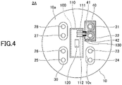
- the wire member 130 can be made even shorter, by routing the first conductive layer 41 and the second conductive layer 42, which extend to the upper surface of the insulating substrate 40, so as to include portions opposing the interconnects 111 and 112, as in a semiconductor package 2A illustrated in FIG. 4 .
- the parasitic inductance can further be reduced, thereby making it even more advantageous from the viewpoint of transmitting the high-frequency signals.
- the first lead 21 and the second lead 22 were made of kovar, and the diameter was 0.3 mm, while the pitch was 0.7 mm.
- a glass substrate having a relative dielectric constant of 5.5 was used for the insulating substrate 40, and the inside diameter of the first through hole 40x and the second through hole 40y was 0.45 mm, and the pitch of the first through hole 40x and the second through hole 40y was 0.7 mm.
- the characteristic impedance ( ⁇ ) was determined for the semiconductor packages 2, 2A, and 2X, results illustrated in FIG. 5 were obtained.
- the ordinate indicates a characteristic impedance Zdiff (ohm: ⁇ ), and the abscissa indicates time (ps).
- the characteristic impedance at 40 (ps) is approximately 120 ( ⁇ ).
- the characteristic impedance is approximately 50 ( ⁇ ) throughout the indicated time range, and it was confirmed that a characteristic impedance close to an ideal characteristic impedance is obtainable.
- a first modification of the first embodiment is an example which enhances a shieldability (or shielding properties) of differential interconnects.
- constituent elements that are the same as those of the first embodiment will be designated by the same reference numerals, and a description thereof may be omitted.
- FIG. 8 is a diagram illustrating an example of the header for the semiconductor package according to a first modification of the first embodiment, and is a partial cross sectional view corresponding to FIG. 1A .
- a third conductive layer 43 can be formed on a side surface of the insulating substrate 40.
- the third conductive layer 43 can be formed of titanium, copper, nickel, gold, or the like, for example.
- the third conductive layer 43 is preferably electrically connected to the eyelet 10 which assumes the GND potential, by the conductive bonding material 50, such as solder or the like.
- the material used for the insulating substrate 40, and the inside diameter and the pitch of the first through hole 40x and the second through hole 40y can be varied to adjust the characteristic impedance.
- a second modification of the first embodiment is an example using a single-end interconnect.
- constituent elements that are the same as those of the first embodiment and the first modification will be designated by the same reference numerals, and a description thereof may be omitted.
- FIG. 9 is a diagram (part 1) illustrating an example of the header for the semiconductor package according to a second modification of the first embodiment, and is a partial cross sectional view corresponding to FIG. 1A .
- the insulating substrate 40 is provided with only one first through hole 40x, and the first lead 21 is the only signal lead.
- the connection between the first lead 21 and the first conductive layer 41 is the same as in the case of differential interconnects.
- the third conductive layer 43 is provided on the side surface of the insulating substrate 40, and the third conductive layer 43 is electrically connected to the eyelet 10 which assumes the GND potential, by the conductive bonding material 50, such as solder or the like.
- Such a configuration ensures a predetermined characteristic impedance even in the case of the single-end interconnect, and can reduce the return of the heat from the eyelet 10 toward the light emitting element 120.
- FIG. 10A and FIG. 10B are diagrams (part 2) illustrating the example of the header for the semiconductor package according to the second modification of the first embodiment.
- the insulating substrate 40 can be provided with one or more third through holes 40z for the GND, in addition to the first through hole 40x for the signal.
- a fourth conductive layer 44 is formed on an inner wall defining the third through hole 40z, and the fourth conductive layer 44 extends to the upper surface of the insulating substrate 40.
- the fourth conductive layer 44 can be formed of titanium, copper, nickel, gold, or the like, for example.
- the fourth conductive layer 44 is electrically connected to the eyelet 10 which assumes the GND potential, by the conductive bonding material 50, such as solder or the like.
- two third through holes 40z are provided, but only one third through hole 40z or three or more third through holes 40z can be provided.
- the third through hole 40z provided in the insulating substrate 40 can have a semi-circular shape or the like in the plan view facing the side surface of the insulating substrate 40.
- the third through hole 40z illustrated in FIG. 10B has a shape corresponding to the third through hole 40z illustrated in FIG. 10A that is cut vertically through the center thereof, and the fourth conductive layer 44 formed on the inner wall defining the third through hole 40z is exposed at the side surface of the insulating substrate 40.
- the fourth conductive layer 44 formed on the inner wall defining the third through hole 40z can easily be electrically connected to the eyelet 10 which assumes the GND potential, by the conductive bonding material 50, such as solder or the like.
- two third through holes 40z are provided, but only one third through hole 40z can be provided.
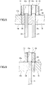
- FIG. 11A and FIG. 11B are diagrams (part 1) illustrating an example of the header for the semiconductor package according to a third modification of the first embodiment.
- Leads such as a first lead 21A and a second lead 22A illustrated in FIG. 11A , can have a nail-like shape that is widened at one end thereof closer to the insulating substrate 40.
- a diameter of the widened portion is larger than the diameter of the first through hole 40x and the second through hole 40y, for example.
- first lead 21A and the second lead 22A are not inserted inside the first through hole 40x and the second through hole 40y, respectively, but instead, upper surfaces of the first lead 21A and the second lead 22A are connected to the first conductive layer 41 by the conductive bonding material 50, such as solder or the like.
- the widened end of the first lead 21B and the second lead 22B can be curved so as to be convex toward the insulating substrate 40.
- the widened end of the first lead 21B and the second lead 22B can have a hemispherical shape, for example.
- the widened end of the first lead 21B and the second lead 22B enters inside the first through hole 40x and the second through hole 40y, respectively. This configuration facilitates positioning of the first lead 21B and the second lead 22B relative to the first through hole 40x and second through hole 40y.
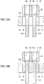
- FIG. 12A and FIG. 12B are diagrams (part 2) illustrating the example of the header for the semiconductor package according to the third modification of the first embodiment.
- a gap can be provided between the upper surface 10a of the eyelet 10 and a lower surface of the insulating substrate 40.
- the gap between the upper surface 10a of the eyelet 10 and the lower surface of the insulating substrate 40 can be in a range of approximately 0 mm to approximately 0.3 mm, for example.
- the parasitic capacitance can be reduced by providing the gap as illustrated in FIG. 12A and FIG. 12B .
- the insulating substrate 40 is formed of a material having a thermal conductivity lower than the thermal conductivity of each lead, a ceramic substrate or the like can be used as the insulating substrate 40.
- the effect of reducing the return of the heat from the eyelet 10 toward the light emitting element 120 is greater in the case of a glass substrate having a thermal conductivity lower than the thermal conductivity of the ceramic substrate. From a viewpoint of controlling the characteristic impedance, the glass substrate and the ceramic substrate exhibit approximately the same effect.
- a resin substrate such as a glass epoxy substrate or the like, can be used as the insulating substrate 40.
Landscapes
- Physics & Mathematics (AREA)
- Condensed Matter Physics & Semiconductors (AREA)
- General Physics & Mathematics (AREA)
- Electromagnetism (AREA)
- Optics & Photonics (AREA)
- Semiconductor Lasers (AREA)
- Cooling Or The Like Of Semiconductors Or Solid State Devices (AREA)
- Geometry (AREA)
Abstract
Description
- The present invention relates to headers for semiconductor packages, and semiconductor packages. The header may sometimes also be referred to as a stem.
- In a semiconductor package provided with a light emitting element, a cooling element for temperature adjustment is provided in a case where an amount of heat generated from the light emitting element is large. In this case, the light emitting element may be provided on a device mounting insulating substrate disposed on the cooling element.
- In the semiconductor package having the configuration described above, a transmission line length from a signal lead to the light emitting element becomes long because the cooling element is relatively thick, and a predetermined characteristic impedance may not be obtainable in some cases. In addition, in order to reduce a decrease in cooling efficiency, considerations need to be taken so that the heat of the light emitting element, transferred by the provision of the cooling element, will not be returned toward the light emitting element.
- Accordingly, in a header for the semiconductor package that can be provided with the light emitting device and the cooling element, considerations also need to be taken so that the configuration of the header enables the desired characteristic impedance and cooling performance of the semiconductor package to be obtained.
- An example of related art is proposed in
Japanese Laid-Open Patent Publication No. 2017-212252 Japanese Patent No. 6,794,140 - Accordingly, it is an object in one aspect of the embodiments to provide a header for a semiconductor package, having a configuration that takes into consideration the characteristic impedance and cooling performance of the semiconductor package.
- According to one aspect of the embodiments, a header for a semiconductor package, includes an eyelet having a through hole penetrating the eyelet from an upper surface to a lower surface of the eyelet; a first lead inserted inside the through hole; and an insulating substrate disposed on the upper surface of the eyelet, and provided with a first through hole at a position overlapping one end of the first lead in a plan view, wherein the insulating substrate has a thermal conductivity lower than a thermal conductivity of the first lead, a first conductive layer is formed on an inner wall defining the first through hole, and the first conductive layer extends to an upper surface of the insulating substrate, the one end of the first lead is electrically connected to the first conductive layer, and a space is provided above the one end of the first lead inside the first through hole.
- The object and advantages of the embodiments will be realized and attained by means of the elements and combinations particularly pointed out in the claims.
- It is to be understood that both the foregoing general description and the following detailed description are exemplary and explanatory and not restrictive of the invention, as claimed.
-
-
FIG. 1A and FIG. 1B are diagrams illustrating an example of a header for a semiconductor package according to a first embodiment; -
FIG. 2A and FIG. 2B are diagrams illustrating an example of a semiconductor package according to the first embodiment; -
FIG. 3A and FIG. 3B are diagrams illustrating an example of a semiconductor package according to a comparative example; -
FIG. 4 is a diagram for explaining a modification of routing a first conductive layer and a second conductive layer; -
FIG. 5 is a diagram (part 1) for explaining simulation results; -
FIG. 6 is a diagram (part 2) for explaining the simulation results; -
FIG. 7 is a diagram (part 3) for explaining the simulation results; -
FIG. 8 is a diagram illustrating an example of the header for the semiconductor package according to a first modification of the first embodiment; -
FIG. 9 is a diagram (part 1) illustrating an example of the header for the semiconductor package according to a second modification of the first embodiment; -
FIG. 10A and FIG. 10B are diagrams (part 2) illustrating the example of the header for the semiconductor package according to the second modification of the first embodiment; -
FIG. 11A and FIG. 11B are diagrams (part 1) illustrating an example of the header for the semiconductor package according to a third modification of the first embodiment; and -
FIG. 12A and FIG. 12B are diagrams (part 2) illustrating the example of the header for the semiconductor package according to the third modification of the first embodiment. - Preferred embodiments of the present invention will be described with reference to the accompanying drawings. In the drawings, those parts that are the same are designated by the same reference numerals, and a repeated description of the same parts may be omitted.
- A description will now be given of a header for a semiconductor package, and a semiconductor package, according to each embodiment of the present invention.
-
FIG. 1A and FIG. 1B are diagrams illustrating an example of a header for a semiconductor package according to a first embodiment.FIG. 1A is a plan view of the header, andFIG. 1B is a partial cross sectional view of the header along a line A-A inFIG. 1A . - As illustrated in
FIG. 1A and FIG. 1B , aheader 1 for a semiconductor package (hereinafter also referred to as a semiconductor package header 1) according to the first embodiment includes aneyelet 10, afirst lead 21, asecond lead 22, athird lead 23, afourth lead 24, afifth lead 25, asixth lead 26, aseventh lead 27, aneighth lead 28, aseal 30, and aninsulating substrate 40. Thesemiconductor package header 1 can be used as a header for optical communication, for example. - When it is not necessary to distinguish the
first lead 21, thesecond lead 22, thethird lead 23, thefourth lead 24, thefifth lead 25, thesixth lead 26, theseventh lead 27, and theeighth lead 28 from one another, each of the first through eighth leads 21 through 28 may simply be referred to as a lead. - The
eyelet 10 is a disk shaped member. A diameter of theeyelet 10 is not particularly limited, and can be appropriately determined according to purpose thereof, and can be 3.8 mm, 5.6 mm, or the like, for example. A thickness of theeyelet 10 is not particularly limited, and can be appropriately determined according to purpose thereof, and can be in a range of approximately 1.0 mm to approximately 1.5 mm, for example. Theeyelet 10 can be formed of a metallic material, such as iron or the like, for example. Theeyelet 10 can be formed of a metallic material (for example, a so-called cladding material) in which a plurality of metal layers (for example, copper layers, iron layers, or the like) are laminated. A gold plating or the like can be provided on a surface of theeyelet 10. - In the present specification, the term "disk shaped member" refers to a member having a planar shape that is approximately circular and having a predetermined thickness. The thickness relative to the diameter of the disk shaped member is not particularly limited, and can be small or large. The disk shaped member can include a concave portion, a convex portion, a through hole, or the like formed in a portion thereof. In the present specification, a plan view of an object refers to a view of the object in a normal direction to an
upper surface 10a of theeyelet 10, and a planar shape of the object refers to a shape of the object in the plan view viewed in the normal direction to theupper surface 10a of theeyelet 10. - One or more cutouts having a shape recessed from an outer periphery towards a center of the
eyelet 10 in the plan view, can be formed at an outer edge of theeyelet 10. The cutout can be a recess having a planar shape that is generally triangular or generally rectangular, for example. The cutout can be used for positioning or the like of a device mounting surface when mounting a semiconductor device on thesemiconductor package header 1, for example. In addition, the cutout can be used for positioning or the like of a rotating direction of thesemiconductor package header 1, for example. - Each lead is inserted into a through
hole 10x that penetrates theeyelet 10 from theupper surface 10a to alower surface 10b thereof, in a state where a longitudinal direction of each lead penetrates a thickness direction of theeyelet 10, and a periphery of each lead is sealed by theseal 30. Theseal 30 is made of an insulating material, such as glass or the like, for example. The glass can be soft glass, typified by soft glass having a relative dielectric constant of approximately 6.7, for example. A single lead can be disposed inside one throughhole 10x, or multiple leads can be disposed inside one throughhole 10x. In the example illustrated inFIG. 1A and FIG. 1B , two leads are disposed inside one throughhole 10x. - A portion of each of the
first lead 21 and thesecond lead 22 protrudes upward from theupper surface 10a of theeyelet 10. A protruding amount of each of thefirst lead 21 and thesecond lead 22 can be in a range of approximately 0.1 mm to approximately 0.3 mm, for example. Leads other than thefirst lead 21 and thesecond lead 22 can also protrude upward from theupper surface 10a of theeyelet 10, as required. Each lead protrudes downward from thelower surface 10b of theeyelet 10. A protruding amount of each lead from thelower surface 10b of theeyelet 10 can be in a range of approximately 6 mm to approximately 10 mm, for example. Each lead can be formed of a metal, such as iron nickel alloy, kovar, or the like, for example, and a gold plating or the like can be provided on a surface of each lead. - The
first lead 21 and thesecond lead 22 are disposed adjacent to each other, and provide a path for differential signaling electrically connected to a light emitting element, when mounting the light emitting element on thesemiconductor package header 1 for use as the semiconductor package. The leads other than thefirst lead 21 and thesecond lead 22 provide a path for a ground GND, a signal path electrically connected to a cooling element mounted on thesemiconductor package header 1, a signal path electrically connected to a temperature sensor mounted on thesemiconductor package header 1, or the like, for example. The number of leads is not particularly limited, and can be increased or decreased, as required. - The insulating
substrate 40 is disposed on theupper surface 10a of theeyelet 10. The insulatingsubstrate 40 is bonded to theupper surface 10a of theeyelet 10 using gold tin (AnSn) solder, silver paste, or the like, for example. The insulatingsubstrate 40 is formed of a material having a thermal conductivity lower than a thermal conductivity of a material forming each lead. More particularly, a glass substrate is preferably used as the insulatingsubstrate 40. Examples of glass forming the glass substrate include alkali-free glass, quartz glass, soda lime glass, borosilicate glass, or the like, for example. - The insulating
substrate 40 can have a parallelepiped shape, for example. A height of the insulatingsubstrate 40 with reference to theupper surface 10a of theeyelet 10 can be in a range of approximately 1 mm to approximately 2 mm, for example. The insulatingsubstrate 40 has a first throughhole 40x at a position overlapping one end of thefirst lead 21 in the plan view. The insulatingsubstrate 40 has a second throughhole 40y at a position overlapping one end of thesecond lead 22 in the plan view. The first throughhole 40x and the second throughhole 40y are provided in a direction parallel to the longitudinal direction of thefirst lead 21 and thesecond lead 22. - A first
conductive layer 41 is formed on an inner wall defining the first throughhole 40x, and the firstconductive layer 41 extends to an upper surface of the insulatingsubstrate 40. In addition, a secondconductive layer 42 is formed on an inner wall defining the second throughhole 40y, and the secondconductive layer 42 extends to the upper surface of the insulatingsubstrate 40. The firstconductive layer 41 and the secondconductive layer 42 can be formed of titanium, copper, nickel, gold, or the like, for example. - The planar shapes of the first through
hole 40x and the second throughhole 40y are circular, for example. An inside diameter of the first throughhole 40x is determined to a value that enables insertion of thefirst lead 21 into the first throughhole 40x. Moreover, an inside diameter of the second throughhole 40y is determined to a value that enables insertion of thesecond lead 22 into the second throughhole 40y. For example, in a case where a diameter of thefirst lead 21 and thesecond lead 22 is 0.3 mm, the inside diameter of the first throughhole 40x and the second throughhole 40y can be 0.45 mm. - One end of the
first lead 21 protrudes from theupper surface 10a of theeyelet 10, and is inserted into the first throughhole 40x. This one end of thefirst lead 21 is electrically connected to the firstconductive layer 41, via aconductive bonding material 50. One end of thesecond lead 22 protrudes from theupper surface 10a of theeyelet 10, and is inserted into the second throughhole 40y. This one end of thesecond lead 22 is electrically connected to the secondconductive layer 42, via theconductive bonding material 50. Theconductive bonding material 50 can be solder (for example, gold tin alloy), a conductive paste (for example, silver paste), or the like, for example. A space is provided above the one end of thefirst lead 21 inside the first throughhole 40x. Further, a space is provided above the one end of thesecond lead 22 inside the second throughhole 40y. -
FIG. 2A and FIG. 2B are diagrams illustrating an example of a semiconductor package according to the first embodiment.FIG. 2A is a plan view of the semiconductor package, andFIG. 2B is a partial cross sectional view of the semiconductor package along a line B-B inFIG. 2A . - As illustrated in
FIG. 2A and FIG. 2B , thesemiconductor package 2 according to the first embodiment includes the semiconductor package header 1 (refer toFIG. 1A and FIG. 1B ), acooling element 100, adevice mounting substrate 110 to be mounted with devices, and alight emitting element 120. In thesemiconductor package 2, a cap, integrally including a lens, a window, or the like for extracting light emitted from thelight emitting element 120, is fixed to thesemiconductor package header 1 by resistance welding or the like. However, because such a configuration of the cap is a well known, an illustration of the cap will be omitted. The cap is formed of a metal, such as stainless steel or the like, for example, and the cap provides an airtight seal for main components, such as thelight emitting element 120 or the like of thesemiconductor package header 1 inside the cap. - The
cooling element 100 is disposed on theupper surface 10a of theeyelet 10. Thecooling element 100 is fixed to theupper surface 10a of theeyelet 10 by a bonding agent or the like having a high thermal conductivity, for example, at a position near the center of theeyelet 10. Thecooling element 100 cools thelight emitting element 120 which generates heat when emitting light, and can be a Peltier element, for example. A cooling capacity of thecooling element 100 is adjusted by varying an external voltage applied to thecooling element 100. - The
device mounting substrate 110 is disposed on thecooling element 100. Thedevice mounting substrate 110 is fixed to thecooling element 100 by a bonding agent or the like having a high thermal conductivity, for example. Thelight emitting element 120 is mounted on thedevice mounting substrate 110. Thelight emitting element 120 can be a semiconductor laser chip that emits light having a wavelength of 1310 nm or the like, for example. -
Interconnects light emitting element 120, are formed on thedevice mounting substrate 110. InFIG. 2A and FIG. 2B , illustration of a portion of theinterconnects interconnects substrate 40 on thedevice mounting substrate 110. Theinterconnect 111 is electrically connected to a portion of the firstconductive layer 41 extending to the upper surface of the insulatingsubstrate 40, via awire member 130. In addition, theinterconnect 112 is electrically connected to a portion of the secondconductive layer 42 extending to the upper surface of the insulatingsubstrate 40, via thewire member 130. Examples of thewire member 130 include a bonding wire or the like, for example. However, thewire member 130 is not particularly limited, as long as thewire member 130 is a wire (or line) shaped member. - The
interconnects interconnect 111, via thefirst lead 21, theconductive bonding material 50, the firstconductive layer 41, and thewire member 130. In addition, a inverted phase signal, obtained by inverting the positive phase signal, is input to theinterconnect 112, via thesecond lead 22, theconductive bonding material 50, the secondconductive layer 42, and thewire member 130. - The
semiconductor package header 1 has a configuration that takes into consideration the characteristic impedance and the cooling performance of the semiconductor package that is formed using thesemiconductor package header 1. This configuration will be described below with reference toFIG. 3A through FIG. 7 , or the like. -
FIG. 3A and FIG. 3B are diagrams illustrating an example a semiconductor package according to a comparative example.FIG. 3A is a plan view of the semiconductor package, andFIG. 3B is a partial cross sectional view of the semiconductor package along a line C-C inFIG. 3A . - As illustrated in
FIG. 3A and FIG. 3B , asemiconductor package 2X according to the comparative example differs from the semiconductor package 2 (refer toFIG. 2A and FIG. 2B ), in that thesemiconductor package 2X does not have an insulatingsubstrate 40, and that one end of thefirst lead 21 and one end of thesecond lead 22 are positioned near the upper surface of thedevice mounting substrate 110. - In the
semiconductor package 2X, protruding amounts of thefirst lead 21 and thesecond lead 22 from theupper surface 10a of theeyelet 10 are large. For this reason, heat caused by the operation of thelight emitting element 120, transferred toward theeyelet 10 by thecooling element 100, is returned toward thelight emitting element 120 via thefirst lead 21 and thesecond lead 22, which have a relatively high thermal conductivity and a relatively large volume. As a result, the cooling efficiency of thecooling element 100 deteriorates, thereby deteriorating the characteristics of thelight emitting element 120 in some cases. - On the other hand, in the
semiconductor package 2, the protruding amounts of thefirst lead 21 and thesecond lead 22 from theupper surface 10a of theeyelet 10 are reduced. In addition, in place of the leads, the firstconductive layer 41 provided inside the first throughhole 40x of the insulatingsubstrate 40, and the secondconductive layer 42 provided inside the second throughhole 40y of the insulatingsubstrate 40, extend to the upper surface of the insulatingsubstrate 40 and connect to thewire member 130. - Because the thermal conductivity of the insulating
substrate 40 is lower than the thermal conductivity of thefirst lead 21 and thesecond lead 22, it is possible to reduce the heat caused by the operation of thelight emitting element 120, transferred toward theeyelet 10 by thecooling element 100, from being returned toward thelight emitting element 120. In addition, because the firstconductive layer 41 and the secondconductive layer 42 are approximately several µm and thin, the firstconductive layer 41 and the secondconductive layer 42 essentially do not contribute to the return of the heat toward thelight emitting element 120. As a result, the cooling efficiency of thecooling element 100 does not deteriorate, thereby enabling thelight emitting element 120 to exhibit predetermined characteristics. - In a case where the
first lead 21 and thesecond lead 22 are formed of kovar, for example, the thermal conductivity thereof is approximately 16.7 W/m•K. On the other hand, when the insulatingsubstrate 40 is formed of glass, the thermal conductivity thereof is approximately 1.1 W/m•K, which is less than 1/10 that of kovar. For this reason, in thesemiconductor package 2, it is possible to greatly reduce the return of the heat from theeyelet 10 toward thelight emitting element 120. - When the protruding amounts of the
first lead 21 inside the first throughhole 40x and thesecond lead 22 inside the second throughhole 40y are set large, the effect of reducing the return of the heat deteriorates. For this reason, the protruding amounts of thefirst lead 21 inside the first throughhole 40x and thesecond lead 22 inside the second throughhole 40y are preferably small within a range that enables reliable bonding between thefirst lead 21 and the firstconductive layer 41, and between thesecond lead 22 and the secondconductive layer 42. - In addition, by disposing the insulating
substrate 40 on theupper surface 10a of theeyelet 10, and adjusting and selecting through hole diameter and through hole pitch (or interval) of the first throughhole 40x and the second throughhole 40y provided in the insulatingsubstrate 40, and a dielectric constant of the insulatingsubstrate 40, it is possible to match the characteristic impedances and reduce return loss. As a result, in thesemiconductor package 2, high-frequency signals can be transmitted to thelight emitting element 120 in an excellent manner. - In the
semiconductor package 2X according to the comparative example, in a case where the diameter of thefirst lead 21 and thesecond lead 22 is 0.3 mm, and the pitch of thefirst lead 21 and thesecond lead 22 is 0.7 mm, a differential impedance of thefirst lead 21 and thesecond lead 22 becomes approximately 170 Ω. - On the other hand, in the
semiconductor package 2, in a case where the inside diameter of the first throughhole 40x and the second throughhole 40y is 0.45 mm, and the pitch of the first throughhole 40x and the second throughhole 40y is 0.7 mm, a differential impedance of thefirst lead 21 and thesecond lead 22 can be approximately 50 Ω. The characteristic impedance can be adjusted by varying the material used for the insulatingsubstrate 40, and the inside diameter and the pitch of the first throughhole 40x and the second throughhole 40y. - In addition, as may be seen from a comparison of the
semiconductor package 2 illustrated inFIG. 2A and FIG. 2B and thesemiconductor package 2X illustrated inFIG. 3A and FIG. 3B , thesemiconductor package 2 can make thewire member 130 short compared to thesemiconductor package 2X, thereby enabling a parasitic inductance to be reduced, which is also advantageous from a viewpoint of transmitting high-frequency signals. In thesemiconductor package 2X, a length of thewire member 130 is approximately 0.65 mm, for example. In contrast, in thesemiconductor package 2, the length of thewire member 130 is approximately 0.31 mm, for example, and can be less than or equal to one-half the length of thewire member 130 in thesemiconductor package 2X. - Moreover, the
wire member 130 can be made even shorter, by routing the firstconductive layer 41 and the secondconductive layer 42, which extend to the upper surface of the insulatingsubstrate 40, so as to include portions opposing theinterconnects semiconductor package 2A illustrated inFIG. 4 . As a result, the parasitic inductance can further be reduced, thereby making it even more advantageous from the viewpoint of transmitting the high-frequency signals. - Next, simulation results for the
semiconductor packages first lead 21 and thesecond lead 22 were made of kovar, and the diameter was 0.3 mm, while the pitch was 0.7 mm. A glass substrate having a relative dielectric constant of 5.5 was used for the insulatingsubstrate 40, and the inside diameter of the first throughhole 40x and the second throughhole 40y was 0.45 mm, and the pitch of the first throughhole 40x and the second throughhole 40y was 0.7 mm. - When the characteristic impedance (Ω) was determined for the
semiconductor packages FIG. 5 were obtained. InFIG. 5 , the ordinate indicates a characteristic impedance Zdiff (ohm: Ω), and the abscissa indicates time (ps). As illustrated inFIG. 5 , in thesemiconductor package 2X having no insulatingsubstrate 40, the characteristic impedance at 40 (ps) is approximately 120 (Ω). On the other hand, in thesemiconductor packages substrate 40, the characteristic impedance is approximately 50 (Ω) throughout the indicated time range, and it was confirmed that a characteristic impedance close to an ideal characteristic impedance is obtainable. - In addition, when the insertion loss (dB) and the return loss (dB) were determined for the
semiconductor packages FIG. 6 andFIG. 7 were obtained. InFIG. 6 , the ordinate indicates the insertion loss (dB), and the abscissa indicates the frequency (GHz). InFIG. 7 , the ordinate indicates the return loss (dB), and the abscissa indicates the frequency (GHz). FromFIG. 6 andFIG. 7 , it can be seen that the insertion loss (dB) and the return loss (dB) up to approximately 15 GHz are significantly improved in thesemiconductor packages substrate 40, when compared to thesemiconductor package 2X having no insulatingsubstrate 40. In particular, thesemiconductor package 2A having theshort wire member 130, the return loss (dB) near 10 GHz is significantly improved. - A first modification of the first embodiment is an example which enhances a shieldability (or shielding properties) of differential interconnects. In the first modification of the first embodiment, constituent elements that are the same as those of the first embodiment will be designated by the same reference numerals, and a description thereof may be omitted.
-
FIG. 8 is a diagram illustrating an example of the header for the semiconductor package according to a first modification of the first embodiment, and is a partial cross sectional view corresponding toFIG. 1A . - As illustrated in
FIG. 8 , a thirdconductive layer 43 can be formed on a side surface of the insulatingsubstrate 40. The thirdconductive layer 43 can be formed of titanium, copper, nickel, gold, or the like, for example. By providing the thirdconductive layer 43 on the side surface of the insulatingsubstrate 40, the shielding of the differential interconnects through the first throughhole 40x and the second throughhole 40y can be enhanced. The thirdconductive layer 43 is preferably electrically connected to theeyelet 10 which assumes the GND potential, by theconductive bonding material 50, such as solder or the like. In a case where the characteristic impedance decreases due to the provision of the thirdconductive layer 43 which assumes the GND potential, the material used for the insulatingsubstrate 40, and the inside diameter and the pitch of the first throughhole 40x and the second throughhole 40y can be varied to adjust the characteristic impedance. - A second modification of the first embodiment is an example using a single-end interconnect. In the second modification of the first embodiment, constituent elements that are the same as those of the first embodiment and the first modification will be designated by the same reference numerals, and a description thereof may be omitted.
-
FIG. 9 is a diagram (part 1) illustrating an example of the header for the semiconductor package according to a second modification of the first embodiment, and is a partial cross sectional view corresponding toFIG. 1A . In the example illustrated inFIG. 9 , the insulatingsubstrate 40 is provided with only one first throughhole 40x, and thefirst lead 21 is the only signal lead. The connection between thefirst lead 21 and the firstconductive layer 41 is the same as in the case of differential interconnects. The thirdconductive layer 43 is provided on the side surface of the insulatingsubstrate 40, and the thirdconductive layer 43 is electrically connected to theeyelet 10 which assumes the GND potential, by theconductive bonding material 50, such as solder or the like. - Such a configuration ensures a predetermined characteristic impedance even in the case of the single-end interconnect, and can reduce the return of the heat from the
eyelet 10 toward thelight emitting element 120. -
FIG. 10A and FIG. 10B are diagrams (part 2) illustrating the example of the header for the semiconductor package according to the second modification of the first embodiment. As illustrated inFIG. 10A , the insulatingsubstrate 40 can be provided with one or more third throughholes 40z for the GND, in addition to the first throughhole 40x for the signal. A fourthconductive layer 44 is formed on an inner wall defining the third throughhole 40z, and the fourthconductive layer 44 extends to the upper surface of the insulatingsubstrate 40. The fourthconductive layer 44 can be formed of titanium, copper, nickel, gold, or the like, for example. The fourthconductive layer 44 is electrically connected to theeyelet 10 which assumes the GND potential, by theconductive bonding material 50, such as solder or the like. In the example illustrated inFIG. 10A , two third throughholes 40z are provided, but only one third throughhole 40z or three or more third throughholes 40z can be provided. - In addition, as illustrated in
FIG. 10B , the third throughhole 40z provided in the insulatingsubstrate 40 can have a semi-circular shape or the like in the plan view facing the side surface of the insulatingsubstrate 40. The third throughhole 40z illustrated inFIG. 10B has a shape corresponding to the third throughhole 40z illustrated inFIG. 10A that is cut vertically through the center thereof, and the fourthconductive layer 44 formed on the inner wall defining the third throughhole 40z is exposed at the side surface of the insulatingsubstrate 40. In this configuration, the fourthconductive layer 44 formed on the inner wall defining the third throughhole 40z can easily be electrically connected to theeyelet 10 which assumes the GND potential, by theconductive bonding material 50, such as solder or the like. In the example illustrated inFIG. 10B , two third throughholes 40z are provided, but only one third throughhole 40z can be provided. - In a third modification of the first embodiment, variation of the lead is illustrated. In the third modification of the first embodiment, constituent elements that are the same as those of the first embodiment, the first modification, and the second modification will be designated by the same reference numerals, and a description thereof may be omitted.
-
FIG. 11A and FIG. 11B are diagrams (part 1) illustrating an example of the header for the semiconductor package according to a third modification of the first embodiment. Leads, such as afirst lead 21A and asecond lead 22A illustrated inFIG. 11A , can have a nail-like shape that is widened at one end thereof closer to the insulatingsubstrate 40. In thefirst lead 21A and thesecond lead 22A, a diameter of the widened portion is larger than the diameter of the first throughhole 40x and the second throughhole 40y, for example. In this case, thefirst lead 21A and thesecond lead 22A are not inserted inside the first throughhole 40x and the second throughhole 40y, respectively, but instead, upper surfaces of thefirst lead 21A and thesecond lead 22A are connected to the firstconductive layer 41 by theconductive bonding material 50, such as solder or the like. - As illustrated in
FIG. 11B , the widened end of thefirst lead 21B and thesecond lead 22B can be curved so as to be convex toward the insulatingsubstrate 40. The widened end of thefirst lead 21B and thesecond lead 22B can have a hemispherical shape, for example. The widened end of thefirst lead 21B and thesecond lead 22B enters inside the first throughhole 40x and the second throughhole 40y, respectively. This configuration facilitates positioning of thefirst lead 21B and thesecond lead 22B relative to the first throughhole 40x and second throughhole 40y. -
FIG. 12A and FIG. 12B are diagrams (part 2) illustrating the example of the header for the semiconductor package according to the third modification of the first embodiment. As illustrated inFIG. 12A and FIG. 12B , a gap can be provided between theupper surface 10a of theeyelet 10 and a lower surface of the insulatingsubstrate 40. The gap between theupper surface 10a of theeyelet 10 and the lower surface of the insulatingsubstrate 40 can be in a range of approximately 0 mm to approximately 0.3 mm, for example. In a case where a parasitic capacitance is observed at a connecting portion between each lead and each of the firstconductive layer 41 and the secondconductive layer 42, the parasitic capacitance can be reduced by providing the gap as illustrated inFIG. 12A and FIG. 12B . - While the preferred embodiments have been described in detail above, various variations, modifications, and substitutions can be made to the embodiments and modifications described above without departing from the scope of the present invention.
- For example, in a case where the insulating
substrate 40 is formed of a material having a thermal conductivity lower than the thermal conductivity of each lead, a ceramic substrate or the like can be used as the insulatingsubstrate 40. However, the effect of reducing the return of the heat from theeyelet 10 toward thelight emitting element 120 is greater in the case of a glass substrate having a thermal conductivity lower than the thermal conductivity of the ceramic substrate. From a viewpoint of controlling the characteristic impedance, the glass substrate and the ceramic substrate exhibit approximately the same effect. In addition, in a case where a material subjectable to a low-temperature heat treatment, such as silver paste or the like, is used as theconductive bonding material 50, a resin substrate, such as a glass epoxy substrate or the like, can be used as the insulatingsubstrate 40. In this case, it is preferable to select a material having a low thermal conductivity in a direction perpendicular to theupper surface 10a of theeyelet 10. - Accordingly to each of the embodiments and modifications described above, it is possible to provide a header for a semiconductor package, having a configuration that takes into consideration the characteristic impedance and cooling performance of the semiconductor package.
- Although the modifications of the embodiments are numbered with, for example, "first," "second," or "third," the ordinal numbers do not imply priorities of the modifications of the embodiments. Many other variations and modifications will be apparent to those skilled in the art.
- All examples and conditional language recited herein are intended for pedagogical purposes to aid the reader in understanding the invention and the concepts contributed by the inventor to furthering the art, and are to be construed as being without limitation to such specifically recited examples and conditions, nor does the organization of such examples in the specification relate to a illustrating of the superiority and inferiority of the invention. Although the embodiments of the present invention have been described in detail, it should be understood that the various changes, substitutions, and alterations could be made hereto without departing from the spirit and scope of the invention.
Claims (10)
- A header (1) for a semiconductor package, (2, 2A) comprising:an eyelet (10) having a through hole (10x) penetrating the eyelet (10) from an upper surface (10a) to a lower surface (10b) of the eyelet (10);a first lead (21, 21A, 21B) inserted inside the through hole (10x); andan insulating substrate (40) disposed on the upper surface (10a) of the eyelet (10), and provided with a first through hole (40x) at a position overlapping one end of the first lead (21, 21A, 21B) in a plan view, whereinthe insulating substrate (40) has a thermal conductivity lower than a thermal conductivity of the first lead (21, 21A, 21B),a first conductive layer (41) is formed on an inner wall defining the first through hole (40x), and the first conductive layer (41) extends to an upper surface of the insulating substrate (40),the one end of the first lead (21, 21A, 21B) is electrically connected to the first conductive layer (41), anda space is provided above the one end of the first lead (21, 21A, 21B) inside the first through hole (40x).
- The header (1) for the semiconductor package (2, 2A) as claimed in claim 1, further comprising:a second lead (22, 22A, 22B) adjacent to the first lead (21, 21A, 21B), whereinthe thermal conductivity of the insulating substrate (40) is lower than thermal conductivities of the first lead (21, 21A, 21B) and the second lead (22, 22A, 22B),the insulating substrate (40) is provided with a second through hole (40y) at a position overlapping one end of the second lead (22, 22A, 22B) in the plan view,a second conductive layer (42) is formed on an inner wall defining the second through hole (22, 22A, 22B), and the second conductive layer (42) extends to the upper surface of the insulating substrate (40),the one end of the second lead (22, 22A, 22B) is electrically connected to the second conductive layer (42), anda space is provided above the one end of the second lead (22, 22A, 22B) inside the second through hole (40y).
- The header (1) for the semiconductor package (2, 2A) as claimed in claim 1 or 2, further comprising:a third conductive layer (43) formed on a side surface of the insulating substrate (40), whereinthe third conductive layer (43) is electrically connected to the eyelet (10).
- The header (1) for the semiconductor package (2, 2A) as claimed in claim 1 or 3, whereinthe insulating substrate (40) is provided with a third through hole (40z),a fourth conductive layer (44) is formed on an inner wall defining the third through hole (40z), andthe fourth conductive layer (44) is electrically connected to the eyelet (10).
- The header (1) for the semiconductor package (2, 2A) as claimed in claim 4, wherein the fourth conductive layer (44) formed on the inner wall defining the third through hole (40z) is exposed at a side surface of the insulating substrate (40).
- The header (1) for the semiconductor package (2, 2A) as claimed in any one of claims 1 to 5, wherein the first lead (21A, 21B) is widened at the one end thereof.
- The header (1) for the semiconductor package (2, 2A) as claimed in claim 6, whereinthe one end of the first lead (21B) is curved so as to be convex toward the insulating substrate (40), anda portion of the one end of the first lead (21B) enters inside the first through hole (40x).
- The header (1) for the semiconductor package (2, 2A) as claimed in claim 6 or 7, wherein a gap is formed between the upper surface of the eyelet (10) and a lower surface of the insulating substrate (40).
- The header (1) for the semiconductor package (2, 2A) as claimed in any one of claims 1 to 8, wherein the insulating substrate (40) is a glass substrate.
- A semiconductor package (2, 2A) comprising:the header (1) for the semiconductor package (2, 2A) as claimed in any one of claims 1 to 9;a cooling element (100) disposed on the upper surface (10a) of the eyelet (10);a substrate (110) disposed on the cooling element (100); anda light emitting element (120) mounted on the substrate (110), whereinan interconnect (111, 112) electrically connecting to the light emitting element (120) is formed on the substrate (110), andthe interconnect (111, 112) is electrically connected to a portion of the first conductive layer (41) extending to the upper surface of the insulating substrate (40) via a wire member (130).
Applications Claiming Priority (1)
| Application Number | Priority Date | Filing Date | Title |
|---|---|---|---|
| JP2021107468A JP7571975B2 (en) | 2021-06-29 | 2021-06-29 | Stems for semiconductor packages, semiconductor packages |
Publications (2)
| Publication Number | Publication Date |
|---|---|
| EP4113589A2 true EP4113589A2 (en) | 2023-01-04 |
| EP4113589A3 EP4113589A3 (en) | 2023-05-03 |
Family
ID=82067401
Family Applications (1)
| Application Number | Title | Priority Date | Filing Date |
|---|---|---|---|
| EP22179286.4A Pending EP4113589A3 (en) | 2021-06-29 | 2022-06-15 | Header for semiconductor package, and semiconductor package |
Country Status (5)
| Country | Link |
|---|---|
| US (1) | US12532589B2 (en) |
| EP (1) | EP4113589A3 (en) |
| JP (1) | JP7571975B2 (en) |
| KR (1) | KR20230002068A (en) |
| CN (1) | CN115548861A (en) |
Citations (1)
| Publication number | Priority date | Publication date | Assignee | Title |
|---|---|---|---|---|
| JP2017212252A (en) | 2016-05-23 | 2017-11-30 | オプト エレクトロニクス ソリューションズ | Optical transmitter and optical module including the same |
Family Cites Families (23)
| Publication number | Priority date | Publication date | Assignee | Title |
|---|---|---|---|---|
| JPH0719856B2 (en) | 1986-04-30 | 1995-03-06 | イビデン株式会社 | Semiconductor mounting board |
| JPH0719857B2 (en) * | 1986-04-30 | 1995-03-06 | イビデン株式会社 | Semiconductor mounting board |
| US6262477B1 (en) * | 1993-03-19 | 2001-07-17 | Advanced Interconnect Technologies | Ball grid array electronic package |
| JPH10284935A (en) | 1997-04-09 | 1998-10-23 | Murata Mfg Co Ltd | Voltage controlled oscillator and method of manufacturing the same |
| JP3167296B2 (en) | 1998-07-31 | 2001-05-21 | 日本特殊陶業株式会社 | Resin wiring board |
| US6855631B2 (en) * | 2003-07-03 | 2005-02-15 | Micron Technology, Inc. | Methods of forming via plugs using an aerosol stream of particles to deposit conductive materials |
| JP4423053B2 (en) * | 2004-01-28 | 2010-03-03 | 京セラ株式会社 | Wiring board |
| JP2007123806A (en) * | 2005-09-29 | 2007-05-17 | Kyocera Corp | Electronic component mounting substrate and electronic device |
| US20080067665A1 (en) | 2006-09-20 | 2008-03-20 | Azniza Binti Abd Aziz | Via structure |
| KR101349582B1 (en) * | 2009-06-02 | 2014-01-09 | 미쓰비시덴키 가부시키가이샤 | Semiconductor light modulating device |
| JP2012160484A (en) | 2009-06-02 | 2012-08-23 | Mitsubishi Electric Corp | Signal transmission module |
| JP5334887B2 (en) * | 2010-02-22 | 2013-11-06 | 京セラ株式会社 | Electronic component mounting package and electronic device using the same |
| JP5766081B2 (en) * | 2011-07-28 | 2015-08-19 | 京セラ株式会社 | Electronic component storage package and electronic device using the same |
| CN107306009B (en) | 2016-04-25 | 2021-04-13 | 住友电工光电子器件创新株式会社 | Light emitter providing coplanar lines on a carrier |
| JP6881746B2 (en) * | 2016-04-25 | 2021-06-02 | 住友電工デバイス・イノベーション株式会社 | Optical semiconductor device |
| US10297724B2 (en) * | 2017-07-10 | 2019-05-21 | Ngk Spark Plug Co., Ltd. | Package for mounting light-emitting device |
| JP6924641B2 (en) * | 2017-07-17 | 2021-08-25 | 日本特殊陶業株式会社 | Light emitting element mounting package and its manufacturing method |
| JP7028587B2 (en) * | 2017-08-31 | 2022-03-02 | 日本ルメンタム株式会社 | Optical module and optical transmission device |
| DE102017123342A1 (en) * | 2017-10-09 | 2019-04-11 | Schott Ag | TO housing with high reflection loss |
| JP7063695B2 (en) * | 2018-04-10 | 2022-05-09 | 日本ルメンタム株式会社 | Optical module |
| US12015242B2 (en) | 2018-11-21 | 2024-06-18 | Mitsubishi Electric Corporation | Optical module |
| TWI681527B (en) | 2019-03-21 | 2020-01-01 | 創意電子股份有限公司 | Circuit structure and chip package |
| JP7350646B2 (en) * | 2019-12-17 | 2023-09-26 | CIG Photonics Japan株式会社 | optical module |
-
2021
- 2021-06-29 JP JP2021107468A patent/JP7571975B2/en active Active
-
2022
- 2022-06-13 US US17/806,572 patent/US12532589B2/en active Active
- 2022-06-15 EP EP22179286.4A patent/EP4113589A3/en active Pending
- 2022-06-20 CN CN202210701203.8A patent/CN115548861A/en active Pending
- 2022-06-22 KR KR1020220076125A patent/KR20230002068A/en active Pending
Patent Citations (2)
| Publication number | Priority date | Publication date | Assignee | Title |
|---|---|---|---|---|
| JP2017212252A (en) | 2016-05-23 | 2017-11-30 | オプト エレクトロニクス ソリューションズ | Optical transmitter and optical module including the same |
| JP6794140B2 (en) | 2016-05-23 | 2020-12-02 | オプト エレクトロニクス ソリューションズ | Optical transmitter and optical module including it |
Also Published As
| Publication number | Publication date |
|---|---|
| US20220416142A1 (en) | 2022-12-29 |
| JP2023005501A (en) | 2023-01-18 |
| KR20230002068A (en) | 2023-01-05 |
| CN115548861A (en) | 2022-12-30 |
| EP4113589A3 (en) | 2023-05-03 |
| JP7571975B2 (en) | 2024-10-23 |
| US12532589B2 (en) | 2026-01-20 |
Similar Documents
| Publication | Publication Date | Title |
|---|---|---|
| KR101430634B1 (en) | Optical Modules | |
| CN106206465B (en) | Semiconductor device header and semiconductor device | |
| US9159634B2 (en) | Transistor outline housing and method for producing same | |
| US10629505B2 (en) | Electronic component mounting package and electronic device using the same | |
| US20140008780A1 (en) | Semiconductor device housing package, and semiconductor apparatus and electronic apparatus including the same | |
| US10512155B2 (en) | Wiring board, optical semiconductor element package, and optical semiconductor device | |
| CN114488431B (en) | Miniaturized high-reliability external modulation light source packaging structure and packaging method | |
| US11923652B2 (en) | Header for semiconductor package, and semiconductor package | |
| US11153962B2 (en) | Header for semiconductor device, and semiconductor device | |
| US6936921B2 (en) | High-frequency package | |
| US12532589B2 (en) | Header for semiconductor package, and semiconductor package | |
| US20240006839A1 (en) | Semiconductor device | |
| US20230344193A1 (en) | Stem for semiconductor package and semiconductor package | |
| JP6671567B1 (en) | Optical module | |
| JP7036646B2 (en) | Packages for semiconductor devices and semiconductor devices | |
| JP4172783B2 (en) | Input/output terminal, semiconductor element storage package, and semiconductor device | |
| JP7534407B2 (en) | Wiring substrate and electronic device | |
| JP2003289149A (en) | Light receiving module | |
| US20220173570A1 (en) | Structure of impedance signal lines for to-can type semiconductor package | |
| JP2004140188A (en) | Package for storing semiconductor elements | |
| JP2003133630A (en) | Semiconductor element storage package and semiconductor device | |
| JP2006179775A (en) | Semiconductor element storage package and semiconductor device | |
| JP2004200242A (en) | Package for storing semiconductor elements | |
| JP2004165507A (en) | Package for storing semiconductor elements | |
| JP2004152826A (en) | Package for storing semiconductor elements |
Legal Events
| Date | Code | Title | Description |
|---|---|---|---|
| PUAI | Public reference made under article 153(3) epc to a published international application that has entered the european phase |
Free format text: ORIGINAL CODE: 0009012 |
|
| STAA | Information on the status of an ep patent application or granted ep patent |
Free format text: STATUS: THE APPLICATION HAS BEEN PUBLISHED |
|
| AK | Designated contracting states |
Kind code of ref document: A2 Designated state(s): AL AT BE BG CH CY CZ DE DK EE ES FI FR GB GR HR HU IE IS IT LI LT LU LV MC MK MT NL NO PL PT RO RS SE SI SK SM TR |
|
| PUAL | Search report despatched |
Free format text: ORIGINAL CODE: 0009013 |
|
| AK | Designated contracting states |
Kind code of ref document: A3 Designated state(s): AL AT BE BG CH CY CZ DE DK EE ES FI FR GB GR HR HU IE IS IT LI LT LU LV MC MK MT NL NO PL PT RO RS SE SI SK SM TR |
|
| RIC1 | Information provided on ipc code assigned before grant |
Ipc: H01L 23/38 20060101ALN20230329BHEP Ipc: H01S 5/02212 20210101ALN20230329BHEP Ipc: H01L 33/48 20100101ALI20230329BHEP Ipc: H01L 23/045 20060101AFI20230329BHEP |
|
| STAA | Information on the status of an ep patent application or granted ep patent |
Free format text: STATUS: REQUEST FOR EXAMINATION WAS MADE |
|
| 17P | Request for examination filed |
Effective date: 20230727 |