EP4113261A1 - Anzeigebildschirmsteuerungsverfahren und elektronische vorrichtung - Google Patents
Anzeigebildschirmsteuerungsverfahren und elektronische vorrichtung Download PDFInfo
- Publication number
- EP4113261A1 EP4113261A1 EP22735282.0A EP22735282A EP4113261A1 EP 4113261 A1 EP4113261 A1 EP 4113261A1 EP 22735282 A EP22735282 A EP 22735282A EP 4113261 A1 EP4113261 A1 EP 4113261A1
- Authority
- EP
- European Patent Office
- Prior art keywords
- display
- region
- capacitance value
- capacitance
- electronic device
- Prior art date
- Legal status (The legal status is an assumption and is not a legal conclusion. Google has not performed a legal analysis and makes no representation as to the accuracy of the status listed.)
- Granted
Links
Images


Classifications
-
- G—PHYSICS
- G06—COMPUTING OR CALCULATING; COUNTING
- G06F—ELECTRIC DIGITAL DATA PROCESSING
- G06F3/00—Input arrangements for transferring data to be processed into a form capable of being handled by the computer; Output arrangements for transferring data from processing unit to output unit, e.g. interface arrangements
- G06F3/01—Input arrangements or combined input and output arrangements for interaction between user and computer
- G06F3/03—Arrangements for converting the position or the displacement of a member into a coded form
- G06F3/041—Digitisers, e.g. for touch screens or touch pads, characterised by the transducing means
- G06F3/0416—Control or interface arrangements specially adapted for digitisers
-
- G—PHYSICS
- G06—COMPUTING OR CALCULATING; COUNTING
- G06F—ELECTRIC DIGITAL DATA PROCESSING
- G06F1/00—Details not covered by groups G06F3/00 - G06F13/00 and G06F21/00
- G06F1/16—Constructional details or arrangements
- G06F1/1613—Constructional details or arrangements for portable computers
- G06F1/1615—Constructional details or arrangements for portable computers with several enclosures having relative motions, each enclosure supporting at least one I/O or computing function
- G06F1/1616—Constructional details or arrangements for portable computers with several enclosures having relative motions, each enclosure supporting at least one I/O or computing function with folding flat displays, e.g. laptop computers or notebooks having a clamshell configuration, with body parts pivoting to an open position around an axis parallel to the plane they define in closed position
-
- G—PHYSICS
- G06—COMPUTING OR CALCULATING; COUNTING
- G06F—ELECTRIC DIGITAL DATA PROCESSING
- G06F1/00—Details not covered by groups G06F3/00 - G06F13/00 and G06F21/00
- G06F1/16—Constructional details or arrangements
- G06F1/1613—Constructional details or arrangements for portable computers
- G06F1/1633—Constructional details or arrangements of portable computers not specific to the type of enclosures covered by groups G06F1/1615 - G06F1/1626
- G06F1/1637—Details related to the display arrangement, including those related to the mounting of the display in the housing
- G06F1/1643—Details related to the display arrangement, including those related to the mounting of the display in the housing the display being associated to a digitizer, e.g. laptops that can be used as penpads
-
- G—PHYSICS
- G06—COMPUTING OR CALCULATING; COUNTING
- G06F—ELECTRIC DIGITAL DATA PROCESSING
- G06F1/00—Details not covered by groups G06F3/00 - G06F13/00 and G06F21/00
- G06F1/16—Constructional details or arrangements
- G06F1/1613—Constructional details or arrangements for portable computers
- G06F1/1633—Constructional details or arrangements of portable computers not specific to the type of enclosures covered by groups G06F1/1615 - G06F1/1626
- G06F1/1675—Miscellaneous details related to the relative movement between the different enclosures or enclosure parts
- G06F1/1677—Miscellaneous details related to the relative movement between the different enclosures or enclosure parts for detecting open or closed state or particular intermediate positions assumed by movable parts of the enclosure, e.g. detection of display lid position with respect to main body in a laptop, detection of opening of the cover of battery compartment
-
- G—PHYSICS
- G06—COMPUTING OR CALCULATING; COUNTING
- G06F—ELECTRIC DIGITAL DATA PROCESSING
- G06F1/00—Details not covered by groups G06F3/00 - G06F13/00 and G06F21/00
- G06F1/16—Constructional details or arrangements
- G06F1/1613—Constructional details or arrangements for portable computers
- G06F1/1633—Constructional details or arrangements of portable computers not specific to the type of enclosures covered by groups G06F1/1615 - G06F1/1626
- G06F1/1684—Constructional details or arrangements related to integrated I/O peripherals not covered by groups G06F1/1635 - G06F1/1675
- G06F1/1694—Constructional details or arrangements related to integrated I/O peripherals not covered by groups G06F1/1635 - G06F1/1675 the I/O peripheral being a single or a set of motion sensors for pointer control or gesture input obtained by sensing movements of the portable computer
-
- G—PHYSICS
- G06—COMPUTING OR CALCULATING; COUNTING
- G06F—ELECTRIC DIGITAL DATA PROCESSING
- G06F1/00—Details not covered by groups G06F3/00 - G06F13/00 and G06F21/00
- G06F1/26—Power supply means, e.g. regulation thereof
- G06F1/32—Means for saving power
- G06F1/3203—Power management, i.e. event-based initiation of a power-saving mode
- G06F1/3206—Monitoring of events, devices or parameters that trigger a change in power modality
- G06F1/3215—Monitoring of peripheral devices
-
- G—PHYSICS
- G06—COMPUTING OR CALCULATING; COUNTING
- G06F—ELECTRIC DIGITAL DATA PROCESSING
- G06F1/00—Details not covered by groups G06F3/00 - G06F13/00 and G06F21/00
- G06F1/26—Power supply means, e.g. regulation thereof
- G06F1/32—Means for saving power
- G06F1/3203—Power management, i.e. event-based initiation of a power-saving mode
- G06F1/3206—Monitoring of events, devices or parameters that trigger a change in power modality
- G06F1/3231—Monitoring the presence, absence or movement of users
-
- G—PHYSICS
- G06—COMPUTING OR CALCULATING; COUNTING
- G06F—ELECTRIC DIGITAL DATA PROCESSING
- G06F1/00—Details not covered by groups G06F3/00 - G06F13/00 and G06F21/00
- G06F1/26—Power supply means, e.g. regulation thereof
- G06F1/32—Means for saving power
- G06F1/3203—Power management, i.e. event-based initiation of a power-saving mode
- G06F1/3234—Power saving characterised by the action undertaken
- G06F1/325—Power saving in peripheral device
- G06F1/3262—Power saving in digitizer or tablet
-
- G—PHYSICS
- G06—COMPUTING OR CALCULATING; COUNTING
- G06F—ELECTRIC DIGITAL DATA PROCESSING
- G06F1/00—Details not covered by groups G06F3/00 - G06F13/00 and G06F21/00
- G06F1/26—Power supply means, e.g. regulation thereof
- G06F1/32—Means for saving power
- G06F1/3203—Power management, i.e. event-based initiation of a power-saving mode
- G06F1/3234—Power saving characterised by the action undertaken
- G06F1/325—Power saving in peripheral device
- G06F1/3265—Power saving in display device
-
- G—PHYSICS
- G06—COMPUTING OR CALCULATING; COUNTING
- G06F—ELECTRIC DIGITAL DATA PROCESSING
- G06F3/00—Input arrangements for transferring data to be processed into a form capable of being handled by the computer; Output arrangements for transferring data from processing unit to output unit, e.g. interface arrangements
- G06F3/01—Input arrangements or combined input and output arrangements for interaction between user and computer
- G06F3/03—Arrangements for converting the position or the displacement of a member into a coded form
- G06F3/041—Digitisers, e.g. for touch screens or touch pads, characterised by the transducing means
- G06F3/044—Digitisers, e.g. for touch screens or touch pads, characterised by the transducing means by capacitive means
-
- G—PHYSICS
- G06—COMPUTING OR CALCULATING; COUNTING
- G06F—ELECTRIC DIGITAL DATA PROCESSING
- G06F3/00—Input arrangements for transferring data to be processed into a form capable of being handled by the computer; Output arrangements for transferring data from processing unit to output unit, e.g. interface arrangements
- G06F3/01—Input arrangements or combined input and output arrangements for interaction between user and computer
- G06F3/048—Interaction techniques based on graphical user interfaces [GUI]
- G06F3/0484—Interaction techniques based on graphical user interfaces [GUI] for the control of specific functions or operations, e.g. selecting or manipulating an object, an image or a displayed text element, setting a parameter value or selecting a range
-
- G—PHYSICS
- G06—COMPUTING OR CALCULATING; COUNTING
- G06F—ELECTRIC DIGITAL DATA PROCESSING
- G06F3/00—Input arrangements for transferring data to be processed into a form capable of being handled by the computer; Output arrangements for transferring data from processing unit to output unit, e.g. interface arrangements
- G06F3/01—Input arrangements or combined input and output arrangements for interaction between user and computer
- G06F3/048—Interaction techniques based on graphical user interfaces [GUI]
- G06F3/0487—Interaction techniques based on graphical user interfaces [GUI] using specific features provided by the input device, e.g. functions controlled by the rotation of a mouse with dual sensing arrangements, or of the nature of the input device, e.g. tap gestures based on pressure sensed by a digitiser
- G06F3/0488—Interaction techniques based on graphical user interfaces [GUI] using specific features provided by the input device, e.g. functions controlled by the rotation of a mouse with dual sensing arrangements, or of the nature of the input device, e.g. tap gestures based on pressure sensed by a digitiser using a touch-screen or digitiser, e.g. input of commands through traced gestures
-
- G—PHYSICS
- G06—COMPUTING OR CALCULATING; COUNTING
- G06F—ELECTRIC DIGITAL DATA PROCESSING
- G06F9/00—Arrangements for program control, e.g. control units
- G06F9/06—Arrangements for program control, e.g. control units using stored programs, i.e. using an internal store of processing equipment to receive or retain programs
- G06F9/44—Arrangements for executing specific programs
- G06F9/451—Execution arrangements for user interfaces
-
- G—PHYSICS
- G06—COMPUTING OR CALCULATING; COUNTING
- G06F—ELECTRIC DIGITAL DATA PROCESSING
- G06F2203/00—Indexing scheme relating to G06F3/00 - G06F3/048
- G06F2203/041—Indexing scheme relating to G06F3/041 - G06F3/045
- G06F2203/04108—Touchless 2D- digitiser, i.e. digitiser detecting the X/Y position of the input means, finger or stylus, also when it does not touch, but is proximate to the digitiser's interaction surface without distance measurement in the Z direction
Definitions
- This application provides a display control method and an electronic device, to determine, based on a change in a capacitance value on a touch panel of a display, whether the display is fastened to a shielding cover, so as to control on and off of the display, and avoid incorrect control of the display.
- the first predetermined condition includes one or a combination of more of the following: An area ratio of the contact region to the detection region exceeds a first ratio; a capacitance value corresponding to the contact region is not less than a capacitance threshold; and existence duration of the contact region exceeds preset duration.
- the first predetermined condition may be that the area ratio of the contact region to the detection region exceeds the first ratio.
- a large-area floating contact and a single-point floating contact are distinguished by using the first predetermined condition. This avoids false control of the display when a hand touches the display.
- the first predetermined condition may be that the existence duration of the contact region exceeds the preset duration.
- the method includes: when the display is on, controlling the acceleration sensor to stop collecting the real-time acceleration value; and when the display changes from on to off, controlling the acceleration sensor to continue to collect the real-time acceleration value.
- the microphone is configured to stop collecting the ambient sound data when the display is on.
- the foregoing one or more processors are further configured to: when the real-time acceleration value indicates that a motion track of the upper cover conforms to a circumferential motion, determine that the first operation is received.
- the foregoing one or more processors are further configured to: when the vibration information indicates that the upper cover meets a vibration condition, determine that the first operation is received.
- the electronic device includes a time of flight TOF sensor.
- the GNSS may include a global positioning system (global positioning system, GPS), a global navigation satellite system (global navigation satellite system, GLONASS), a beidou navigation satellite system (beidou navigation satellite system, BDS), a quasi-zenith satellite system (quasi-zenith satellite system, QZSS), and/or a satellite based augmentation system (satellite based augmentation systems, SBAS).
- GPS global positioning system
- GLONASS global navigation satellite system
- BDS Bertdou navigation satellite system
- BDS quasi-zenith satellite system
- QZSS quasi-zenith satellite system
- SBAS satellite based augmentation system
- the display 194 is configured to display an image, a video, and the like.
- the display 194 includes a display panel.
- the display panel may use a liquid crystal display (liquid crystal display, LCD), an organic light-emitting diode (organic light-emitting diode, OLED), an active-matrix organic light emitting diode (active-matrix organic light emitting diode, AMOLED), a flexible light-emitting diode (flex light-emitting diode, FLED), a Miniled, a MicroLed, a Micro-oLed, a quantum dot light emitting diode (quantum dot light emitting diodes, QLED), and the like.
- LCD liquid crystal display
- OLED organic light-emitting diode
- AMOLED active-matrix organic light emitting diode
- FLED flexible light-emitting diode
- Miniled a MicroLed, a Micro-oLed, a quantum dot light emit
- the camera 193 is configured to capture a still image or a video. An optical image of an object is generated through the lens, and the image is projected to the light-sensitive element.
- the light-sensitive element may be a charge coupled device (charge coupled device, CCD) or a complementary metal-oxide-semiconductor (complementary metal-oxide-semiconductor, CMOS) phototransistor.
- CCD charge coupled device
- CMOS complementary metal-oxide-semiconductor
- the light-sensitive element converts an optical signal into an electrical signal, and then transmits the electrical signal to the ISP, so that the ISP converts the electrical signal into a digital image signal.
- the ISP outputs the digital image signal to the DSP for processing.
- the DSP converts the digital image signal into an image signal in a standard format such as RGB or YUV.
- the notebook computer may include one or N cameras 193, where N is a positive integer greater than 1.
- the video codec is configured to compress or decompress a digital video.
- the notebook computer may support one or more video codecs. In this way, the notebook computer may play or record videos in a plurality of coding formats, for example, moving picture experts group (moving picture experts group MPEG) 1, MPEG 2, MPEG 3, and MPEG 4.
- moving picture experts group MPEG moving picture experts group
- MPEG 2 moving picture experts group
- MPEG 3 moving picture experts group
- the detection of the change in the capacitance value of the display is actually detection performed on a touch panel of the display.
- the touch panel may also be referred to as a panel.
- a capacitance value of the panel may be obtained by using a touch chip corresponding to the touch panel.
- the current on the panel may be kept at a relatively stable value.
- the current at the contact position on the panel changes.
- a capacitance value of the contact position also changes. For example, when the touch panel is in floating contact with a conductor, a capacitance value of a contact position increases. When the touch panel is in actual contact with the conductor, a capacitance value of a contact position changes to zero. When there is no contact between the touch panel and the conductor, the capacitance value of the touch panel remains stable.
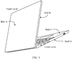
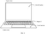
- the first region also referred to as a contact region, is obtained based on an increase in the capacitance value of the touch panel. Whether the C-shell surface of the notebook computer is in contact with the B-shell surface is detected through analysis of the first region.
- the foregoing first region includes all location points whose capacitance values exceed a normal value (which may also be referred to as a first value) on the lower panel at a same moment.
- the foregoing normal value is an average capacitance value on the touch panel when the touch panel is not touched.
- capacitance information of the panel may be obtained by using the touch chip on a frame-by-frame basis.
- Capacitance information of each frame includes capacitance values of all location points on the lower panel at the same moment. Therefore, the collected capacitance information of the current frame may be compared with capacitance information of a previous adjacent frame. For example, first, a first location point is determined on the panel based on the capacitance information of the current frame and the capacitance information of the previous adjacent frame, that is, a location point at which a capacitance value changes is determined.
- all the C-shell surface of the notebook computer may have a conductive characteristic.
- the attribute information of the first region may include one or more items such as an area, a capacitance value, and existence duration of the first region.
- capacitance value changes caused by floating contact between different conductor media and the panel are different.
- a capacitance at the contact position is a capacitance value 1.
- a capacitance at the contact position is a capacitance value 2.
- the capacitance value 1 is obviously less than the capacitance value 2.
- the capacitance value corresponding to each location point in the first region may be periodically detected.
- a capacitance value detected at a current moment is compared with a capacitance value detected at a previous moment adjacent to the current moment. If a difference between a capacitance value of each location point in the first region at the current moment and a capacitance value of each location point at the previous adjacent moment does not exceed a preset threshold 2, it is determined that the first region is in an existed state.
- a preset threshold 2 is a fluctuation amplitude of the capacitance on the panel when the touch panel is in floating contact with the C-shell surface.
- the preset threshold 2 may alternatively be obtained by means of testing in advance.
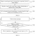
- a ratio of the area of the first region to the area of the detection region is obtained. It is determined whether the area ratio is not less than the first ratio. When the area ratio is not less than the first ratio, a capacitance value of each location point in the first region is obtained. It is determined whether the capacitance value of each location point in the first region is not less than a capacitance threshold. When the capacitance value of each location point in the first region is not less than the capacitance threshold, the existence duration of the first region is obtained. It is determined whether the existence duration of the first region exceeds preset duration. When the existence duration of the first region exceeds the preset duration, it is determined that the B-shell surface is fastened to the C-shell surface.
- the display in a case in which it is determined that the B-shell surface and the C-shell surface are not fastened, the display may be controlled to be on.
- S202 is used to determine whether the B-shell surface is separated from the C-shell surface
- S102 is used to determine whether the B-shell surface is fastened to the C-shell surface.
- a determining logic corresponding to S202 and a determining logic corresponding to S102 are exactly the opposite.
- the notebook computer when the user separates the B-shell surface from the C-shell surface of the notebook computer, a structure of the notebook computer sounds, which is also referred to as a cover opening sound.
- the notebook computer has a locking part.
- the locking part is configured to keep the upper cover (on the side on which the B-shell surface is disposed) and the lower cover (on the side on which the C-shell surface is disposed) of the notebook computer in a fastened state. If the user wants to separate the upper cover and the lower cover, the locking part needs to be opened first to release locking of the fastened state between the upper cover and the lower cover. When the locking part is opened, the locking part makes a sound, and the sound may be considered as a cover opening sound.
- an acceleration sensor is disposed on the upper cover of the notebook computer.
- the foregoing display control method is applied to the notebook computer in a closed-cover state, on the basis of FIG. 8 , as shown in FIG. 10 , the foregoing display control method further includes the following steps.
- the procedure may enter S201. However, after the procedure enters S201, if it is determined, by using S201 and S202, that the C-shell surface is not separated from the B-shell surface, the capacitive value in the detection region stops to continue to be obtained, so as to wait for a next restart detection to be triggered.
- S501 Collect vibration information of the upper cover of the notebook computer, for example, a vibration frequency and a vibration amplitude.
- a TOF sensor may be disposed on the B-shell surface.
- the TOF sensor detects ambient light, it is determined that the B-shell surface is not shielded, that is, the touch panel is not shielded.
- the TOF sensor detects no ambient light, it is determined that the B-shell surface is shielded, that is, the touch panel is shielded.
- the foregoing method may further include: stopping continuing to obtain a capacitance value in the detection region.
- the foregoing one or more processors are further configured to: when the vibration information indicates that the upper cover meets a vibration condition, determine that the first operation is received.
- a working mode of each component (for example, the display, the microphone, and the acceleration sensor) in the electronic device may be flexibly adjusted in different scenarios.
- the frame rate of the display is adjusted based on a scenario (that is, a frame rate at which the display detects a capacitance change condition on the panel).
- the microphone, the acceleration sensor, and the like are enabled to work in a period in which the cover of the electronic device is closed. When the cover of the electronic device is opened, the microphone, the acceleration sensor, and the like are controlled to enter a sleep mode. Therefore, energy saving is achieved.
Landscapes
- Engineering & Computer Science (AREA)
- Theoretical Computer Science (AREA)
- General Engineering & Computer Science (AREA)
- Physics & Mathematics (AREA)
- General Physics & Mathematics (AREA)
- Human Computer Interaction (AREA)
- Computer Hardware Design (AREA)
- Software Systems (AREA)
- Mathematical Physics (AREA)
- User Interface Of Digital Computer (AREA)
- Position Input By Displaying (AREA)
Applications Claiming Priority (2)
| Application Number | Priority Date | Filing Date | Title |
|---|---|---|---|
| CN202110560597.5A CN115390687A (zh) | 2021-05-21 | 2021-05-21 | 一种显示屏控制方法及电子设备 |
| PCT/CN2022/072601 WO2022242211A1 (zh) | 2021-05-21 | 2022-01-18 | 一种显示屏控制方法及电子设备 |
Publications (3)
| Publication Number | Publication Date |
|---|---|
| EP4113261A1 true EP4113261A1 (de) | 2023-01-04 |
| EP4113261A4 EP4113261A4 (de) | 2023-08-23 |
| EP4113261B1 EP4113261B1 (de) | 2024-12-11 |
Family
ID=83558234
Family Applications (1)
| Application Number | Title | Priority Date | Filing Date |
|---|---|---|---|
| EP22735282.0A Active EP4113261B1 (de) | 2021-05-21 | 2022-01-18 | Anzeigebildschirmsteuerungsverfahren und elektronische vorrichtung |
Country Status (4)
| Country | Link |
|---|---|
| US (1) | US12498813B2 (de) |
| EP (1) | EP4113261B1 (de) |
| CN (1) | CN115390687A (de) |
| WO (1) | WO2022242211A1 (de) |
Families Citing this family (2)
| Publication number | Priority date | Publication date | Assignee | Title |
|---|---|---|---|---|
| CN118131856A (zh) * | 2022-12-01 | 2024-06-04 | 荣耀终端有限公司 | 一种电子设备及其控制方法 |
| JP2024123997A (ja) * | 2023-03-02 | 2024-09-12 | キヤノン株式会社 | 電子機器、電子機器の制御方法、およびプログラム |
Family Cites Families (18)
| Publication number | Priority date | Publication date | Assignee | Title |
|---|---|---|---|---|
| US8681124B2 (en) * | 2009-09-22 | 2014-03-25 | Microsoft Corporation | Method and system for recognition of user gesture interaction with passive surface video displays |
| US8478306B2 (en) * | 2010-11-10 | 2013-07-02 | Google Inc. | Self-aware profile switching on a mobile computing device |
| US9159293B2 (en) * | 2011-03-16 | 2015-10-13 | Kyocera Corporation | Electronic device, control method, and storage medium storing control program |
| US9652091B1 (en) * | 2013-03-15 | 2017-05-16 | Amazon Technologies, Inc. | Touch sensitive display utilizing mutual capacitance and self capacitance |
| KR20150077667A (ko) * | 2013-12-30 | 2015-07-08 | 삼성전자주식회사 | 전자 장치, 그 제어 방법 및 컴퓨터 판독가능 기록매체 |
| RU2016135018A (ru) | 2014-01-28 | 2018-03-02 | Хуавей Дивайс (Дунгуань) Ко., Лтд | Способ обработки устройства терминала и устройство терминала |
| KR20160033507A (ko) * | 2014-09-18 | 2016-03-28 | 엘지전자 주식회사 | 이동 단말기 및 그 제어 방법 |
| CN107046601A (zh) | 2017-03-24 | 2017-08-15 | 努比亚技术有限公司 | 一种移动终端及屏幕控制方法 |
| CN114710585B (zh) * | 2017-11-23 | 2023-10-13 | 华为技术有限公司 | 一种拍照方法、终端及存储介质 |
| JP2019145997A (ja) * | 2018-02-20 | 2019-08-29 | オンキヨー株式会社 | 携帯端末 |
| CN108304061A (zh) | 2018-04-16 | 2018-07-20 | 维沃移动通信有限公司 | 一种显示控制方法及终端 |
| US10725595B2 (en) * | 2018-04-24 | 2020-07-28 | Apple Inc. | Electronic devices with covers |
| CN109257505B (zh) | 2018-11-07 | 2021-06-29 | 维沃移动通信有限公司 | 一种屏幕控制方法及移动终端 |
| CN109840061A (zh) | 2019-01-31 | 2019-06-04 | 华为技术有限公司 | 控制屏幕显示的方法及电子设备 |
| US11379016B2 (en) | 2019-05-23 | 2022-07-05 | Intel Corporation | Methods and apparatus to operate closed-lid portable computers |
| CN110660329B (zh) | 2019-09-29 | 2021-12-14 | 武汉天马微电子有限公司 | 一种柔性显示模组及柔性显示装置 |
| CN118426615A (zh) | 2019-11-18 | 2024-08-02 | 荣耀终端有限公司 | 一种防误触方法、移动设备及计算机可读存储介质 |
| US11789565B2 (en) | 2020-08-18 | 2023-10-17 | Intel Corporation | Lid controller hub architecture for improved touch experiences |
-
2021
- 2021-05-21 CN CN202110560597.5A patent/CN115390687A/zh active Pending
-
2022
- 2022-01-18 WO PCT/CN2022/072601 patent/WO2022242211A1/zh not_active Ceased
- 2022-01-18 EP EP22735282.0A patent/EP4113261B1/de active Active
- 2022-01-18 US US17/790,733 patent/US12498813B2/en active Active
Also Published As
| Publication number | Publication date |
|---|---|
| US20240168582A1 (en) | 2024-05-23 |
| EP4113261A4 (de) | 2023-08-23 |
| CN115390687A (zh) | 2022-11-25 |
| WO2022242211A1 (zh) | 2022-11-24 |
| US12498813B2 (en) | 2025-12-16 |
| EP4113261B1 (de) | 2024-12-11 |
Similar Documents
| Publication | Publication Date | Title |
|---|---|---|
| EP4221164B1 (de) | Anzeigeverfahren für eine elektronische vorrichtung mit flexibler anzeige und elektronische vorrichtung | |
| US12160536B2 (en) | Touchscreen, electronic device, and display control method | |
| US11994918B2 (en) | Electronic device control method and electronic device | |
| US11871328B2 (en) | Method for identifying specific position on specific route and electronic device | |
| US11907526B2 (en) | Touch region adjustment method and apparatus for determining a grasping gesture of a user on an electronic device | |
| CN113448482B (zh) | 触控屏的滑动响应控制方法及装置、电子设备 | |
| WO2020073288A1 (zh) | 一种触发电子设备执行功能的方法及电子设备 | |
| EP4113261A1 (de) | Anzeigebildschirmsteuerungsverfahren und elektronische vorrichtung | |
| CN113821129B (zh) | 一种显示窗口控制方法及电子设备 | |
| KR20160105245A (ko) | 터치 패널의 입력을 감지하는 전자 장치 및 방법 | |
| CN116027919B (zh) | 触摸屏的控制方法、电子设备、芯片及存储介质 | |
| WO2023202525A1 (zh) | 功能启动方法、用户界面及电子设备 | |
| CN110058729A (zh) | 调节触摸检测的灵敏度的方法和电子设备 | |
| CN117130701B (zh) | 一种应用程序的图标显示方法及电子设备 | |
| HK40079053A (en) | Display controlling method and electronic device | |
| CN118585056A (zh) | 一种处理器的频率控制方法及电子设备 | |
| CN116048196A (zh) | 开合盖检测方法及相关装置 | |
| CN116954727A (zh) | 一种设备唤醒方法、电子设备及可读存储介质 | |
| CN115033129A (zh) | 握持方式识别方法、装置、设备及存储介质 | |
| CN114115513B (zh) | 一种按键控制方法和一种按键装置 | |
| CN110096151B (zh) | 一种手势识别方法、设备及计算机可读存储介质 | |
| WO2025130040A1 (zh) | 一种触控识别方法及电子设备 | |
| WO2025156636A1 (zh) | 执行落袋检测的方法和终端设备 | |
| CN118820185A (zh) | 文件操作方法、电子设备及计算机可读存储介质 | |
| HK40071116B (en) | Touch screen, electronic device, and display control method |
Legal Events
| Date | Code | Title | Description |
|---|---|---|---|
| STAA | Information on the status of an ep patent application or granted ep patent |
Free format text: STATUS: UNKNOWN |
|
| STAA | Information on the status of an ep patent application or granted ep patent |
Free format text: STATUS: THE INTERNATIONAL PUBLICATION HAS BEEN MADE |
|
| PUAI | Public reference made under article 153(3) epc to a published international application that has entered the european phase |
Free format text: ORIGINAL CODE: 0009012 |
|
| STAA | Information on the status of an ep patent application or granted ep patent |
Free format text: STATUS: REQUEST FOR EXAMINATION WAS MADE |
|
| 17P | Request for examination filed |
Effective date: 20220713 |
|
| AK | Designated contracting states |
Kind code of ref document: A1 Designated state(s): AL AT BE BG CH CY CZ DE DK EE ES FI FR GB GR HR HU IE IS IT LI LT LU LV MC MK MT NL NO PL PT RO RS SE SI SK SM TR |
|
| A4 | Supplementary search report drawn up and despatched |
Effective date: 20230721 |
|
| RIC1 | Information provided on ipc code assigned before grant |
Ipc: G06F 1/3215 20190101ALI20230717BHEP Ipc: G06F 1/3234 20190101ALI20230717BHEP Ipc: G06F 1/16 20060101ALI20230717BHEP Ipc: G06F 3/041 20060101AFI20230717BHEP |
|
| STAA | Information on the status of an ep patent application or granted ep patent |
Free format text: STATUS: EXAMINATION IS IN PROGRESS |
|
| 17Q | First examination report despatched |
Effective date: 20240214 |
|
| GRAP | Despatch of communication of intention to grant a patent |
Free format text: ORIGINAL CODE: EPIDOSNIGR1 |
|
| STAA | Information on the status of an ep patent application or granted ep patent |
Free format text: STATUS: GRANT OF PATENT IS INTENDED |
|
| INTG | Intention to grant announced |
Effective date: 20240710 |
|
| DAV | Request for validation of the european patent (deleted) | ||
| DAX | Request for extension of the european patent (deleted) | ||
| GRAS | Grant fee paid |
Free format text: ORIGINAL CODE: EPIDOSNIGR3 |
|
| GRAA | (expected) grant |
Free format text: ORIGINAL CODE: 0009210 |
|
| STAA | Information on the status of an ep patent application or granted ep patent |
Free format text: STATUS: THE PATENT HAS BEEN GRANTED |
|
| AK | Designated contracting states |
Kind code of ref document: B1 Designated state(s): AL AT BE BG CH CY CZ DE DK EE ES FI FR GB GR HR HU IE IS IT LI LT LU LV MC MK MT NL NO PL PT RO RS SE SI SK SM TR |
|
| REG | Reference to a national code |
Ref country code: GB Ref legal event code: FG4D |
|
| REG | Reference to a national code |
Ref country code: CH Ref legal event code: EP |
|
| REG | Reference to a national code |
Ref country code: DE Ref legal event code: R096 Ref document number: 602022008661 Country of ref document: DE |
|
| REG | Reference to a national code |
Ref country code: IE Ref legal event code: FG4D |
|
| REG | Reference to a national code |
Ref country code: NL Ref legal event code: FP |
|
| REG | Reference to a national code |
Ref country code: LT Ref legal event code: MG9D |
|
| PG25 | Lapsed in a contracting state [announced via postgrant information from national office to epo] |
Ref country code: HR Free format text: LAPSE BECAUSE OF FAILURE TO SUBMIT A TRANSLATION OF THE DESCRIPTION OR TO PAY THE FEE WITHIN THE PRESCRIBED TIME-LIMIT Effective date: 20241211 |
|
| PGFP | Annual fee paid to national office [announced via postgrant information from national office to epo] |
Ref country code: DE Payment date: 20241217 Year of fee payment: 4 |
|
| PG25 | Lapsed in a contracting state [announced via postgrant information from national office to epo] |
Ref country code: FI Free format text: LAPSE BECAUSE OF FAILURE TO SUBMIT A TRANSLATION OF THE DESCRIPTION OR TO PAY THE FEE WITHIN THE PRESCRIBED TIME-LIMIT Effective date: 20241211 |
|
| PG25 | Lapsed in a contracting state [announced via postgrant information from national office to epo] |
Ref country code: BG Free format text: LAPSE BECAUSE OF FAILURE TO SUBMIT A TRANSLATION OF THE DESCRIPTION OR TO PAY THE FEE WITHIN THE PRESCRIBED TIME-LIMIT Effective date: 20241211 |
|
| PG25 | Lapsed in a contracting state [announced via postgrant information from national office to epo] |
Ref country code: ES Free format text: LAPSE BECAUSE OF FAILURE TO SUBMIT A TRANSLATION OF THE DESCRIPTION OR TO PAY THE FEE WITHIN THE PRESCRIBED TIME-LIMIT Effective date: 20241211 |
|
| PG25 | Lapsed in a contracting state [announced via postgrant information from national office to epo] |
Ref country code: NO Free format text: LAPSE BECAUSE OF FAILURE TO SUBMIT A TRANSLATION OF THE DESCRIPTION OR TO PAY THE FEE WITHIN THE PRESCRIBED TIME-LIMIT Effective date: 20250311 |
|
| PG25 | Lapsed in a contracting state [announced via postgrant information from national office to epo] |
Ref country code: GR Free format text: LAPSE BECAUSE OF FAILURE TO SUBMIT A TRANSLATION OF THE DESCRIPTION OR TO PAY THE FEE WITHIN THE PRESCRIBED TIME-LIMIT Effective date: 20250312 Ref country code: LV Free format text: LAPSE BECAUSE OF FAILURE TO SUBMIT A TRANSLATION OF THE DESCRIPTION OR TO PAY THE FEE WITHIN THE PRESCRIBED TIME-LIMIT Effective date: 20241211 |
|
| PG25 | Lapsed in a contracting state [announced via postgrant information from national office to epo] |
Ref country code: RS Free format text: LAPSE BECAUSE OF FAILURE TO SUBMIT A TRANSLATION OF THE DESCRIPTION OR TO PAY THE FEE WITHIN THE PRESCRIBED TIME-LIMIT Effective date: 20250311 |
|
| REG | Reference to a national code |
Ref country code: AT Ref legal event code: MK05 Ref document number: 1750909 Country of ref document: AT Kind code of ref document: T Effective date: 20241211 |
|
| PG25 | Lapsed in a contracting state [announced via postgrant information from national office to epo] |
Ref country code: SM Free format text: LAPSE BECAUSE OF FAILURE TO SUBMIT A TRANSLATION OF THE DESCRIPTION OR TO PAY THE FEE WITHIN THE PRESCRIBED TIME-LIMIT Effective date: 20241211 |
|
| PG25 | Lapsed in a contracting state [announced via postgrant information from national office to epo] |
Ref country code: PL Free format text: LAPSE BECAUSE OF FAILURE TO SUBMIT A TRANSLATION OF THE DESCRIPTION OR TO PAY THE FEE WITHIN THE PRESCRIBED TIME-LIMIT Effective date: 20241211 |
|
| PG25 | Lapsed in a contracting state [announced via postgrant information from national office to epo] |
Ref country code: IS Free format text: LAPSE BECAUSE OF FAILURE TO SUBMIT A TRANSLATION OF THE DESCRIPTION OR TO PAY THE FEE WITHIN THE PRESCRIBED TIME-LIMIT Effective date: 20250411 |
|
| PG25 | Lapsed in a contracting state [announced via postgrant information from national office to epo] |
Ref country code: PT Free format text: LAPSE BECAUSE OF FAILURE TO SUBMIT A TRANSLATION OF THE DESCRIPTION OR TO PAY THE FEE WITHIN THE PRESCRIBED TIME-LIMIT Effective date: 20250411 |
|
| PG25 | Lapsed in a contracting state [announced via postgrant information from national office to epo] |
Ref country code: EE Free format text: LAPSE BECAUSE OF FAILURE TO SUBMIT A TRANSLATION OF THE DESCRIPTION OR TO PAY THE FEE WITHIN THE PRESCRIBED TIME-LIMIT Effective date: 20241211 |
|
| PG25 | Lapsed in a contracting state [announced via postgrant information from national office to epo] |
Ref country code: RO Free format text: LAPSE BECAUSE OF FAILURE TO SUBMIT A TRANSLATION OF THE DESCRIPTION OR TO PAY THE FEE WITHIN THE PRESCRIBED TIME-LIMIT Effective date: 20241211 Ref country code: AT Free format text: LAPSE BECAUSE OF FAILURE TO SUBMIT A TRANSLATION OF THE DESCRIPTION OR TO PAY THE FEE WITHIN THE PRESCRIBED TIME-LIMIT Effective date: 20241211 |
|
| PG25 | Lapsed in a contracting state [announced via postgrant information from national office to epo] |
Ref country code: SK Free format text: LAPSE BECAUSE OF FAILURE TO SUBMIT A TRANSLATION OF THE DESCRIPTION OR TO PAY THE FEE WITHIN THE PRESCRIBED TIME-LIMIT Effective date: 20241211 |
|
| PG25 | Lapsed in a contracting state [announced via postgrant information from national office to epo] |
Ref country code: CZ Free format text: LAPSE BECAUSE OF FAILURE TO SUBMIT A TRANSLATION OF THE DESCRIPTION OR TO PAY THE FEE WITHIN THE PRESCRIBED TIME-LIMIT Effective date: 20241211 |
|
| PG25 | Lapsed in a contracting state [announced via postgrant information from national office to epo] |
Ref country code: IT Free format text: LAPSE BECAUSE OF FAILURE TO SUBMIT A TRANSLATION OF THE DESCRIPTION OR TO PAY THE FEE WITHIN THE PRESCRIBED TIME-LIMIT Effective date: 20241211 |
|
| REG | Reference to a national code |
Ref country code: CH Ref legal event code: PL |
|
| PG25 | Lapsed in a contracting state [announced via postgrant information from national office to epo] |
Ref country code: SE Free format text: LAPSE BECAUSE OF FAILURE TO SUBMIT A TRANSLATION OF THE DESCRIPTION OR TO PAY THE FEE WITHIN THE PRESCRIBED TIME-LIMIT Effective date: 20241211 |
|
| REG | Reference to a national code |
Ref country code: DE Ref legal event code: R097 Ref document number: 602022008661 Country of ref document: DE |
|
| PG25 | Lapsed in a contracting state [announced via postgrant information from national office to epo] |
Ref country code: LU Free format text: LAPSE BECAUSE OF NON-PAYMENT OF DUE FEES Effective date: 20250118 Ref country code: MC Free format text: LAPSE BECAUSE OF FAILURE TO SUBMIT A TRANSLATION OF THE DESCRIPTION OR TO PAY THE FEE WITHIN THE PRESCRIBED TIME-LIMIT Effective date: 20241211 |
|
| PG25 | Lapsed in a contracting state [announced via postgrant information from national office to epo] |
Ref country code: DK Free format text: LAPSE BECAUSE OF FAILURE TO SUBMIT A TRANSLATION OF THE DESCRIPTION OR TO PAY THE FEE WITHIN THE PRESCRIBED TIME-LIMIT Effective date: 20241211 |
|
| PG25 | Lapsed in a contracting state [announced via postgrant information from national office to epo] |
Ref country code: BE Free format text: LAPSE BECAUSE OF NON-PAYMENT OF DUE FEES Effective date: 20250131 |
|
| PLBE | No opposition filed within time limit |
Free format text: ORIGINAL CODE: 0009261 |
|
| STAA | Information on the status of an ep patent application or granted ep patent |
Free format text: STATUS: NO OPPOSITION FILED WITHIN TIME LIMIT |
|
| PG25 | Lapsed in a contracting state [announced via postgrant information from national office to epo] |
Ref country code: CH Free format text: LAPSE BECAUSE OF NON-PAYMENT OF DUE FEES Effective date: 20250131 |
|
| REG | Reference to a national code |
Ref country code: BE Ref legal event code: MM Effective date: 20250131 |
|
| 26N | No opposition filed |
Effective date: 20250912 |
|
| PGFP | Annual fee paid to national office [announced via postgrant information from national office to epo] |
Ref country code: GB Payment date: 20251204 Year of fee payment: 5 |
|
| PG25 | Lapsed in a contracting state [announced via postgrant information from national office to epo] |
Ref country code: FR Free format text: LAPSE BECAUSE OF NON-PAYMENT OF DUE FEES Effective date: 20250211 |
|
| PGFP | Annual fee paid to national office [announced via postgrant information from national office to epo] |
Ref country code: NL Payment date: 20251215 Year of fee payment: 5 |
|
| PG25 | Lapsed in a contracting state [announced via postgrant information from national office to epo] |
Ref country code: IE Free format text: LAPSE BECAUSE OF NON-PAYMENT OF DUE FEES Effective date: 20250118 |