EP4106206A1 - A/d conversion device - Google Patents
A/d conversion device Download PDFInfo
- Publication number
- EP4106206A1 EP4106206A1 EP22188717.7A EP22188717A EP4106206A1 EP 4106206 A1 EP4106206 A1 EP 4106206A1 EP 22188717 A EP22188717 A EP 22188717A EP 4106206 A1 EP4106206 A1 EP 4106206A1
- Authority
- EP
- European Patent Office
- Prior art keywords
- port
- output port
- resistor
- switching element
- conversion device
- Prior art date
- Legal status (The legal status is an assumption and is not a legal conclusion. Google has not performed a legal analysis and makes no representation as to the accuracy of the status listed.)
- Pending
Links
Images



Classifications
-
- H—ELECTRICITY
- H03—ELECTRONIC CIRCUITRY
- H03M—CODING; DECODING; CODE CONVERSION IN GENERAL
- H03M1/00—Analogue/digital conversion; Digital/analogue conversion
- H03M1/12—Analogue/digital converters
- H03M1/34—Analogue value compared with reference values
- H03M1/36—Analogue value compared with reference values simultaneously only, i.e. parallel type
- H03M1/361—Analogue value compared with reference values simultaneously only, i.e. parallel type having a separate comparator and reference value for each quantisation level, i.e. full flash converter type
- H03M1/362—Analogue value compared with reference values simultaneously only, i.e. parallel type having a separate comparator and reference value for each quantisation level, i.e. full flash converter type the reference values being generated by a resistive voltage divider
-
- H—ELECTRICITY
- H03—ELECTRONIC CIRCUITRY
- H03M—CODING; DECODING; CODE CONVERSION IN GENERAL
- H03M1/00—Analogue/digital conversion; Digital/analogue conversion
- H03M1/10—Calibration or testing
- H03M1/1071—Measuring or testing
- H03M1/1076—Detection or location of converter hardware failure, e.g. power supply failure, open or short circuit
-
- H—ELECTRICITY
- H03—ELECTRONIC CIRCUITRY
- H03M—CODING; DECODING; CODE CONVERSION IN GENERAL
- H03M1/00—Analogue/digital conversion; Digital/analogue conversion
- H03M1/10—Calibration or testing
- H03M1/1071—Measuring or testing
-
- H—ELECTRICITY
- H03—ELECTRONIC CIRCUITRY
- H03M—CODING; DECODING; CODE CONVERSION IN GENERAL
- H03M1/00—Analogue/digital conversion; Digital/analogue conversion
- H03M1/12—Analogue/digital converters
- H03M1/1205—Multiplexed conversion systems
- H03M1/122—Shared using a single converter or a part thereof for multiple channels, e.g. a residue amplifier for multiple stages
- H03M1/1225—Shared using a single converter or a part thereof for multiple channels, e.g. a residue amplifier for multiple stages using time-division multiplexing
-
- H—ELECTRICITY
- H03—ELECTRONIC CIRCUITRY
- H03M—CODING; DECODING; CODE CONVERSION IN GENERAL
- H03M1/00—Analogue/digital conversion; Digital/analogue conversion
- H03M1/12—Analogue/digital converters
- H03M1/1205—Multiplexed conversion systems
- H03M1/123—Simultaneous, i.e. using one converter per channel but with common control or reference circuits for multiple converters
Definitions
- the present invention relates to an A/D conversion device which converts analog quantities to digital quantities.
- the usage pattern of the A/D converter disclosed in PTL 1 is such that a plurality of items of information to be inputted are selectively switched by a switch and inputted into an MPU (Micro-processing unit). This configuration enables the number of items of input information to be increased without increasing the number of A/D converters.
- this kind of heretofore known device is simply such as to suppress the number of A/D converters, and in this system, as a switch which switches items of input information is added, it is also necessary to enhance a failure diagnosis function for the switch, and in this case, the necessity cannot help but be met by providing an additional circuit separately.
- the number of A/D converters can be suppressed, but it is impossible to detect anomalies of the A/D converter itself and a device connected to the A/D converter, and the necessity for the anomaly detection has arisen.
- the invention having been contrived in light of the heretofore mentioned actual circumstances, has an object of providing an A/D conversion device which, as well as suppressing the number of A/D converters using a minimum necessary additional part, detects anomalies of the A/D converter itself and a device connected to the A/D converter.
- the A/D conversion device is an A/D conversion device including: an A/D converter which converts analog electricity quantities of objects to be detected to digital quantities; switching circuits which connect a plurality of the analog electricity quantities to the A/D converter; and a control section which controls the switching circuits independently of each other, the A/D conversion device being characterized in that
- the A/D conversion device of the invention there are the advantages that a large number of analog electrical signals targeted as signals to be incorporated can be sequentially converted to digital signals by an A/D converter, and incorporated, without increasing the number of A/D converters, and furthermore, that a failure diagnosis function can be added using a simple additional circuit.
- Fig. 1 is a block diagram of an A/D conversion device according to Embodiment 1 of the invention.
- an A/D conversion device 100A is configured so that a control section 2 can control and output the analog electricity quantities of a first object 4 and a second object 5, independently of each other, via a switching circuit 3 to an A/D converter 1.
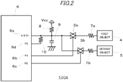
- Fig. 2 is a circuit diagram of the A/D conversion device 100A and shows the state in which a CPU 6 has the built-in A/D converter 1 shown in Fig. 1 .
- the CPU 6 has an A/D port (A/D#1) 6a and ordinary first, second, and third output ports (P1, P2, and P3) 6b, 6c, and 6d. Electrical signals which the first object 4 and second object 5 output are outputted through a first series resistor 7a and a second series resistor 7b, via a first switching circuit 3a and a second switching circuit 3b which are controlled by the first output port 6b and the second output port 6c, respectively, to the A/D port 6a.
- the first switching circuit 3a and the second switching circuit 3b are each configured of an analog switch.
- the first object 4 and the second object 5 generate electrical signals which change independently of each other, and each signal is transmitted to the A/D port 6a in response to an on operation of the first switching circuit 3a or the second switching circuit 3b connected respectively to the first object 4 or the second object 5.
- a first resistor 8 (hereafter referred to as a pull-up resistor 8) and a capacitor 9, other than the A/D port 6a, are connected to the common terminal of the first switching circuit 3a and the second switching circuit 3b with respect respectively to a power source Vcc and the ground, and furthermore, are connected to the third port 6d via a second resistor 10 (hereafter referred to as a pull-down resistor 10), thus configuring an interface circuit.
- the A/D conversion device 100A according to Embodiment 1 is configured by the first object 4 and second object 5 being connected to one A/D port 6a.
- a description will be given of an operation of the A/D conversion device 100A according to Embodiment 1.
- Fig. 3 is a time chart describing an operation of the A/D conversion device 100A according to Embodiment 1.
- the symbol A1 shows the operating state of the second output port 6c
- the symbol B1 shows the operating state of the first output port 6b
- the symbol C1 shows the operating state of the third output port 6d, each of which is shown along the passage of time T.
- the symbol D1 shows the input state of the A/D port 6a.
- the second output port 6c Low
- the first output port 6b High
- the third output port 6d High-Z (Z is impedance) .
- the second switching circuit 3b connected to the second output port 6c is off controlled
- the path of the pull-down resistor 10 connected to the third output port 6d is placed in an open state
- the first switching circuit 3a connected to the first output port 6b is on controlled.
- the signal from the first object 4 is inputted into the A/D port 6a by way of a voltage dividing circuit formed of the first series resistor 7a and the pull-up resistor 8, and only the signal from the first object 4 is incorporated into the CPU 6.
- the signals generated by the first object 4 and the second object 5 are, independently of each other, inputted into one A/D port 6a, and the CPU 6 can acquire the values of the signals .
- the above is the content implemented by a heretofore known device.
- the A/D conversion device 100A according to Embodiment 1 is such that a failure diagnosis is also carried out by adding another simple control, subsequently to the input of the heretofore known device.
- both the first output port 6b and the second output port 6c are set to Low
- the third output port 6d is set to High-Z
- both the first switching circuit 3a and the second switching circuit 3b are off controlled
- the path of the pull-down resistor 10 is placed in an open state, thus preventing the signals from the first object 4 and the second object 5 being connected to the A/D port 6a.
- the pull-up resistor 8 is connected in this state, approximately the same voltage as the voltage of the power source Vcc which is the other connection point of the pull-up resistor 8 is inputted into the A/D port 6a.
- the A/D conversion device 100A When the A/D conversion device 100A is normal, the voltage of the power source Vcc is inputted, but when a voltage other than the voltage of the power source Vcc is inputted, it can be determined that the A/D conversion device 100A is in an anomalous state.
- both the first output port 6b and the second output port 6c are set to High, both the first switching circuit 3a and the second switching circuit 3b are kept to on, and both signal inputs from the first object 4 and the second object 5 are placed in the state of being connected to the A/D port 6a (the third output port 6d is set to High-Z, and the path of the pull-down resistor 10 is placed in an open state).
- the combined voltage of the signals from the first object 4 and the second object 5 are inputted into the A/D port 6a by a voltage combining/dividing circuit formed of the pull-up resistor 8, the first series resistor 7a connected to the first object 4, and the second series resistor 7b connected to the second object 5 in the same way.
- the signals from the first object 4 and the second object 5 are incorporated for the time t2 to t3 and the time t3 to t4, and the constant of the voltage combining/dividing circuit is also known, it thus being possible to confirm the validity of the combined voltage.
- an open/short circuit / resistance anomaly of the first series resistor 7a and the second series resistor 7b, an open failure of the first switching circuit 3a or the second switching circuit 3b, a poor L fixation of at least either the first output port 6b or the second output port 6c, or an anomaly of the A/D converter 1 can be detected as a failure by voltage identification for the time t4 to t5.
- the device is anomalous when the voltages inputted into the A/D port 6a for the time t0 to t1 and the time t1 to t2 of Fig. 3 are each a voltage other than the voltage of the power source Vcc or a resistor divided voltage wherein the voltage of the power source Vcc is divided by the pull-up resistor 8 and the pull-down resistor 10, or when the voltage inputted into the A/D port 6a for the time t4 to t5 is not in alignment with a calculation based on the signal incorporation values of the first object 4 and the second object 5 for the time t2 to t3 and the time t3 to t4, it is possible to increase the number of A/D conversion channels, and at the same time, to include a switching circuit and also a failure detection function of the A/D converter 1, without complicating the configuration of the first switching circuit 3a and the second switching circuit 3b, and therefore, it is possible to improve the reliability of a signal conversion result.
- Fig. 4 is a circuit diagram of an A/D conversion device 100B according to Embodiment 2, and shows the state in which the CPU 6 has the built-in A/D converter 1 shown in Fig. 1 .
- the CPU 6 has the A/D port (A/D#1) 6a and the ordinary first, second, and third output ports (P1, P2, and P3) 6b, 6c, and 6d.
- a first sensor 40 and a second sensor 41 similar to the first sensor 40 are connected in parallel to the A/D port 6a.
- the first sensor 40 and second sensor 41 are such that their respective resistance values Rt1 and Rt2 change in response to the characteristics of the first and second sensors.
- the first and second sensors are one whose resistance value changes by being movable like a potentiometer or thermistor which has a resistance change due to a temperature change.
- the first sensor 40 and the second sensor 41 are pulled up to the power source Vcc via the pull-up resistor 8.
- a first switching element 42 and a second switching element 43 are connected in series, respectively, to the first sensor 40 and the second sensor 41.
- the first switching element 42 and the second switching element 43 are controlled by being connected respectively to the first output port 6b and the second output port 6c.
- the capacitor 9 is connected to the A/D port 6a for the purpose of noise suppression.
- the A/D port 6a is connected to the third output port 6d via the pull-down resistor 10.
- Fig. 5 is a time chart describing an operation of the A/D conversion device 100B according to Embodiment 2.
- the symbol A2 shows an operating state of the second output port 6c
- the symbol B2 shows an operating state of the first output port 6b
- the symbol C2 shows an operating state of the third output port 6d, each of which is shown along the passage of time T.
- the symbol D2 shows an input condition of the A/D port 6a.
- the second output port 6c Low
- the first output port 6b High
- the third output port 6d High-Z (Z is impedance) .
- the second switching element 43 connected to the second output port 6c is off controlled, the path of the pull-down resistor 10 is placed in an open state, and the first switching element 42 connected to the first output port 6b is on controlled.
- the first switching element 42 on, only the first sensor 40 is connected, and the second sensor 41 is in an open state. Because of this, a voltage division ratio between the resistance value Rt1 of the first sensor 40 and the resistance value of the pull-up resistor 8 is inputted into the A/D port 6a.
- the A/D conversion device 100B according to Embodiment 2 also carries out a failure determination by adding another simple control, subsequently to the input of the heretofore known device.
- both the first output port 6b and the second output port 6c are set to Low, both the first switching element 42 and the second switching element 43 are off controlled, and the first sensor 40 and the second sensor 41 are not connected.
- the third output port 6d is set to High-Z, and the path of the pull-down resistor 10 is placed in an open state. As only the pull-up resistor 8 is connected in this state, approximately the same voltage as the voltage of the power source Vcc which is the other connection point of the pull-up resistor 8 is inputted into the A/D port 6a.
- both the first output port 6b and the second output port 6c are set to High, both the first switching element 42 and the second switching element 43 are turned on, the third output port 6d is set to High-Z, and the first sensor 40 and the second sensor 41 are placed in the state of being connected. That is, the first sensor 40 and the second sensor 41 are in the state of being connected in parallel. Because of this, it can be determined that there is a failure unless a value lower than the values of the first sensor 40 and the second sensor 41 inputted for the time t2 to t4 is attained.
- converting means such as a look-up table
- a failure of the first sensor 40 and/or the second sensor 41, a failure of the first switching element 42, the second switching element 43, the first output port 6b, the second output port 6c, or the third output port 6d, or the like, can be considered as a failure mode, but in any case, the values of the first sensor 40 and the second sensor 41 inputted for the time t2 to t4 cannot be determined as true values.
- the values acquired by the first sensor 40 and the second sensor 41 can also be determined to be normal.
- the time chart shown in Fig. 5 shows one example of the operation, and it is free to set a switching pattern as far as the individual modes can be realized in sequence.
- a time chart such as shown in Fig. 6
- A3, B3, C3, and D3 of Fig. 6 show operating states corresponding to A2, B2, C2, and D2 of Fig. 5 , respectively.
- a bipolar transistor is exemplified as the switching element, but the invention not being limited to this, as far as the switching element is an element, such as a MOSFET, an analog switch IC, or a mechanical relay, which has conduction/cutoff characteristics which can be satisfactory after taking into consideration the required precision of A/D conversion on application, it goes without saying that it is possible to use the element freely.
- the switching element is an element, such as a MOSFET, an analog switch IC, or a mechanical relay, which has conduction/cutoff characteristics which can be satisfactory after taking into consideration the required precision of A/D conversion on application, it goes without saying that it is possible to use the element freely.
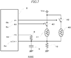
- Fig. 7 is a circuit diagram of an A/D conversion device 100C according to Embodiment 3.
- the first switching element 42 and the second switching element 43 are connected to the ground side, but may be connected to the power source Vcc side as shown in Fig. 7 .
- the pull-up resistor 8 of Fig. 4 is connected to the ground side as the pull-down resistor 10.
- a check target is the pull-down resistor 10
- the first output port 6b and the second output port 6c are set to Low
- the third output port 6d is set to High
- both the first switching element 42 and the second switching element 43 are turned off
- the first sensor 40 and the second sensor 41 are not connected.
- the path of the pull-up resistor 8 is placed in an on state.
- An A/D conversion device comprising:
- the A/D conversion device characterized in that in the second mode, an anomaly of the A/D conversion device is detected with reference to a power source voltage connected to the A/D converter, in the third mode, an anomaly of a part connected to the A/D converter is detected based on the A/D conversion values, and in the fourth mode, an anomaly of a device connected to the A/D converter is detected based on the A/D conversion values.
- the A/D conversion device comprising:
- the A/D conversion device comprising:
Landscapes
- Engineering & Computer Science (AREA)
- Theoretical Computer Science (AREA)
- Analogue/Digital Conversion (AREA)
Abstract
Description
- The present invention relates to an A/D conversion device which converts analog quantities to digital quantities.
- Heretofore, there has been a CPU which holds a plurality of A/D converters which convert analog quantities to a form of digital quantities which a CPU (Central Processing Unit) or the like can use. In recent years, analog signals which the CPU inputs with one system are increasing, and the absolute number of A/D converters (A/D ports in the CPU) is deficient. Thus, for example, as is disclosed in
JP-A-2007-333574 - The usage pattern of the A/D converter disclosed in
PTL 1 is such that a plurality of items of information to be inputted are selectively switched by a switch and inputted into an MPU (Micro-processing unit). This configuration enables the number of items of input information to be increased without increasing the number of A/D converters. - However, this kind of heretofore known device is simply such as to suppress the number of A/D converters, and in this system, as a switch which switches items of input information is added, it is also necessary to enhance a failure diagnosis function for the switch, and in this case, the necessity cannot help but be met by providing an additional circuit separately.
- Thus, the present inventors and others have proposed an A/D conversion device wherein it is possible to add a failure diagnosis function without increasing the number of A/D converters and without providing an additional circuit, as disclosed in
JP-A-2013-225781 - PTL 1:
JP-A-2007-333574 - PTL 2:
JP-A-2013-225781 - In the A/D conversion device disclosed in
PTL 2, the number of A/D converters can be suppressed, but it is impossible to detect anomalies of the A/D converter itself and a device connected to the A/D converter, and the necessity for the anomaly detection has arisen. - The invention, having been contrived in light of the heretofore mentioned actual circumstances, has an object of providing an A/D conversion device which, as well as suppressing the number of A/D converters using a minimum necessary additional part, detects anomalies of the A/D converter itself and a device connected to the A/D converter.
- The A/D conversion device according to the invention is an A/D conversion device including: an A/D converter which converts analog electricity quantities of objects to be detected to digital quantities; switching circuits which connect a plurality of the analog electricity quantities to the A/D converter; and a control section which controls the switching circuits independently of each other, the A/D conversion device being characterized in that
- the control section causes to be generated
- a first mode in which to output the analog electricity quantities of the objects one by one independently to the A/D converter, a second mode in which to output none of the analog electricity quantities of the objects, a third mode in which to output none of the analog electricity quantities of the objects and cause the output to the A/D converter to be pulled down by a resistor, and a fourth mode in which to output to the A/D converter a plurality of the analog electricity quantities of the objects at the same time,
- thus acquiring the A/D conversion values of the objects individually when in the first mode, and detecting an anomaly of the A/D converter itself or a device connected to the A/D converter when in the second mode to the fourth mode.
- According to the A/D conversion device of the invention, there are the advantages that a large number of analog electrical signals targeted as signals to be incorporated can be sequentially converted to digital signals by an A/D converter, and incorporated, without increasing the number of A/D converters, and furthermore, that a failure diagnosis function can be added using a simple additional circuit.
- The foregoing and other objects, features, aspects and advantages of the present invention will become more apparent from the following detailed description of the present invention when taken in conjunction with the accompanying drawings.
-
- [
Fig. 1] Fig. 1 is a block diagram of an A/D conversion device according toEmbodiment 1 of the invention. - [
Fig. 2] Fig. 2 is a circuit diagram of the A/D conversion device according toEmbodiment 1 of the invention. - [
Fig. 3] Fig. 3 is a time chart describing an operation of the A/D conversion device according toEmbodiment 1 of the invention. - [
Fig. 4] Fig. 4 is a circuit diagram of an A/D conversion device according toEmbodiment 2 of the invention. - [
Fig. 5] Fig. 5 is a time chart describing an operation of the A/D conversion device according toEmbodiment 2 of the invention. - [
Fig. 6] Fig. 6 is another time chart describing an operation of the A/D conversion device according toEmbodiment 2 of the invention. - [
Fig. 7] Fig. 7 is a circuit diagram of an A/D conversion device according toEmbodiment 3 of the invention. - Hereafter, a detailed description will be given, with reference to the drawings, of preferred embodiments of an A/D conversion device according to the invention.
-
Fig. 1 is a block diagram of an A/D conversion device according toEmbodiment 1 of the invention. InFig. 1 , an A/D conversion device 100A is configured so that acontrol section 2 can control and output the analog electricity quantities of afirst object 4 and asecond object 5, independently of each other, via aswitching circuit 3 to an A/D converter 1. -
Fig. 2 is a circuit diagram of the A/D conversion device 100A and shows the state in which aCPU 6 has the built-in A/D converter 1 shown inFig. 1 . TheCPU 6 has an A/D port (A/D#1) 6a and ordinary first, second, and third output ports (P1, P2, and P3) 6b, 6c, and 6d. Electrical signals which thefirst object 4 andsecond object 5 output are outputted through afirst series resistor 7a and asecond series resistor 7b, via afirst switching circuit 3a and asecond switching circuit 3b which are controlled by thefirst output port 6b and thesecond output port 6c, respectively, to the A/D port 6a. Thefirst switching circuit 3a and thesecond switching circuit 3b are each configured of an analog switch. - The
first object 4 and thesecond object 5 generate electrical signals which change independently of each other, and each signal is transmitted to the A/D port 6a in response to an on operation of thefirst switching circuit 3a or thesecond switching circuit 3b connected respectively to thefirst object 4 or thesecond object 5. A first resistor 8 (hereafter referred to as a pull-up resistor 8) and acapacitor 9, other than the A/D port 6a, are connected to the common terminal of thefirst switching circuit 3a and thesecond switching circuit 3b with respect respectively to a power source Vcc and the ground, and furthermore, are connected to thethird port 6d via a second resistor 10 (hereafter referred to as a pull-down resistor 10), thus configuring an interface circuit. - As shown in the heretofore mentioned circuit diagram, the A/
D conversion device 100A according toEmbodiment 1 is configured by thefirst object 4 andsecond object 5 being connected to one A/D port 6a. Next, a description will be given of an operation of the A/D conversion device 100A according toEmbodiment 1. -
Fig. 3 is a time chart describing an operation of the A/D conversion device 100A according toEmbodiment 1. InFig. 3 , the symbol A1 shows the operating state of thesecond output port 6c, the symbol B1 shows the operating state of thefirst output port 6b, and the symbol C1 shows the operating state of thethird output port 6d, each of which is shown along the passage of time T. Also, the symbol D1 shows the input state of the A/D port 6a. - First, as a first mode, when focusing on time t2 to t3 of
Fig. 3 , thesecond output port 6c = Low, thefirst output port 6b = High, and thethird output port 6d = High-Z (Z is impedance) . This represents that thesecond switching circuit 3b connected to thesecond output port 6c is off controlled, the path of the pull-down resistor 10 connected to thethird output port 6d is placed in an open state, and thefirst switching circuit 3a connected to thefirst output port 6b is on controlled. By only thefirst switching circuit 3a being on controlled, the signal from thefirst object 4 is inputted into the A/D port 6a by way of a voltage dividing circuit formed of thefirst series resistor 7a and the pull-up resistor 8, and only the signal from thefirst object 4 is incorporated into theCPU 6. - Next, when focusing on time t3 to t4 of
Fig. 3 , in the same way as heretofore mentioned, by only thesecond switching circuit 3b being on controlled, only the signal from thesecond object 5 is inputted into the A/D port 6a, and only the signal from thesecond object 5 is incorporated into theCPU 6 by way of a voltage dividing circuit formed of thesecond series resistor 7b and the pull-up resistor 8. - By the two controls, the signals generated by the
first object 4 and thesecond object 5 are, independently of each other, inputted into one A/D port 6a, and theCPU 6 can acquire the values of the signals . The above is the content implemented by a heretofore known device. - Next, the A/
D conversion device 100A according toEmbodiment 1 is such that a failure diagnosis is also carried out by adding another simple control, subsequently to the input of the heretofore known device. - First, as a second mode, for time t0 to t1 of
Fig. 3 , both thefirst output port 6b and thesecond output port 6c are set to Low, thethird output port 6d is set to High-Z, both thefirst switching circuit 3a and thesecond switching circuit 3b are off controlled, and the path of the pull-down resistor 10 is placed in an open state, thus preventing the signals from thefirst object 4 and thesecond object 5 being connected to the A/D port 6a. As only the pull-up resistor 8 is connected in this state, approximately the same voltage as the voltage of the power source Vcc which is the other connection point of the pull-up resistor 8 is inputted into the A/D port 6a. When the A/D conversion device 100A is normal, the voltage of the power source Vcc is inputted, but when a voltage other than the voltage of the power source Vcc is inputted, it can be determined that the A/D conversion device 100A is in an anomalous state. - That is, there is the possibility of an open state of the pull-
up resistor 8, a short circuit failure of thefirst switching circuit 3a or thesecond switching circuit 3b, a poor H fixation of at least either thefirst output port 6b or thesecond output port 6c, a poor L fixation of thethird output port 6d, or an anomaly of the A/D converter 1, and this is a failure detection state. - Next, as a third mode, for time t1 to t2 of
Fig. 3 , all thefirst output port 6b, thesecond output port 6c, and thethird output port 6d are set to Low, both thefirst switching circuit 3a and thesecond switching circuit 3b are turned off, and the path of the pull-down resistor 10 is placed in an on state. In this case, a voltage wherein the voltage of the power source Vcc is divided by the pull-up resistor 8 and the pull-down resistor 10 is inputted into the A/D port 6a, but when it is confirmed in the heretofore mentioned that the power source Vcc is normal, and when a voltage deviating from a voltage which is assumed in the case of a normal resistance value is inputted, it can be determined that there is a resistance value anomaly of the pull-up resistor 8 or the pull-downresistor 10. - Finally, as a fourth mode, for time t4 to t5 of
Fig. 3 , both thefirst output port 6b and thesecond output port 6c are set to High, both thefirst switching circuit 3a and thesecond switching circuit 3b are kept to on, and both signal inputs from thefirst object 4 and thesecond object 5 are placed in the state of being connected to the A/D port 6a (thethird output port 6d is set to High-Z, and the path of the pull-down resistor 10 is placed in an open state). In this case, the combined voltage of the signals from thefirst object 4 and thesecond object 5 are inputted into the A/D port 6a by a voltage combining/dividing circuit formed of the pull-up resistor 8, thefirst series resistor 7a connected to thefirst object 4, and thesecond series resistor 7b connected to thesecond object 5 in the same way. When switching operations for the time t0 to t5 are of a sufficiently high speed with respect to a change in the signals generated by thefirst object 4 and thesecond object 5, the signals from thefirst object 4 and thesecond object 5 are incorporated for the time t2 to t3 and the time t3 to t4, and the constant of the voltage combining/dividing circuit is also known, it thus being possible to confirm the validity of the combined voltage. - That is, an open/short circuit / resistance anomaly of the
first series resistor 7a and thesecond series resistor 7b, an open failure of thefirst switching circuit 3a or thesecond switching circuit 3b, a poor L fixation of at least either thefirst output port 6b or thesecond output port 6c, or an anomaly of the A/D converter 1 can be detected as a failure by voltage identification for the time t4 to t5. - In other words, as it is determined that the device is anomalous when the voltages inputted into the A/
D port 6a for the time t0 to t1 and the time t1 to t2 ofFig. 3 are each a voltage other than the voltage of the power source Vcc or a resistor divided voltage wherein the voltage of the power source Vcc is divided by the pull-upresistor 8 and the pull-downresistor 10, or when the voltage inputted into the A/D port 6a for the time t4 to t5 is not in alignment with a calculation based on the signal incorporation values of thefirst object 4 and thesecond object 5 for the time t2 to t3 and the time t3 to t4, it is possible to increase the number of A/D conversion channels, and at the same time, to include a switching circuit and also a failure detection function of the A/D converter 1, without complicating the configuration of thefirst switching circuit 3a and thesecond switching circuit 3b, and therefore, it is possible to improve the reliability of a signal conversion result. - In the heretofore mentioned, a description has been given of two detection objects and one A/D port, but the invention not being limited to this, the same advantages can also be obtained when still more objects are connected to one A/D port.
- Next, a description will be given of an A/D conversion device according to
Embodiment 2 of the invention.Fig. 4 is a circuit diagram of an A/D conversion device 100B according toEmbodiment 2, and shows the state in which theCPU 6 has the built-in A/D converter 1 shown inFig. 1 . TheCPU 6 has the A/D port (A/D#1) 6a and the ordinary first, second, and third output ports (P1, P2, and P3) 6b, 6c, and 6d. Afirst sensor 40 and asecond sensor 41 similar to thefirst sensor 40 are connected in parallel to the A/D port 6a. Thefirst sensor 40 andsecond sensor 41 are such that their respective resistance values Rt1 and Rt2 change in response to the characteristics of the first and second sensors. For example, the first and second sensors are one whose resistance value changes by being movable like a potentiometer or thermistor which has a resistance change due to a temperature change. - The
first sensor 40 and thesecond sensor 41 are pulled up to the power source Vcc via the pull-upresistor 8. Also, afirst switching element 42 and asecond switching element 43, each of which is formed of a bipolar transistor, are connected in series, respectively, to thefirst sensor 40 and thesecond sensor 41. Thefirst switching element 42 and thesecond switching element 43 are controlled by being connected respectively to thefirst output port 6b and thesecond output port 6c. Thecapacitor 9 is connected to the A/D port 6a for the purpose of noise suppression. Also, the A/D port 6a is connected to thethird output port 6d via the pull-down resistor 10. -
Fig. 5 is a time chart describing an operation of the A/D conversion device 100B according toEmbodiment 2. InFig. 5 , the symbol A2 shows an operating state of thesecond output port 6c, the symbol B2 shows an operating state of thefirst output port 6b, and the symbol C2 shows an operating state of thethird output port 6d, each of which is shown along the passage of time T. Also, the symbol D2 shows an input condition of the A/D port 6a. - First, as a first mode, when focusing on time t2 to t3 of
Fig. 5 , thesecond output port 6c = Low, thefirst output port 6b = High, and thethird output port 6d = High-Z (Z is impedance) . This represents that thesecond switching element 43 connected to thesecond output port 6c is off controlled, the path of the pull-down resistor 10 is placed in an open state, and thefirst switching element 42 connected to thefirst output port 6b is on controlled. By thefirst switching element 42 = on, only thefirst sensor 40 is connected, and thesecond sensor 41 is in an open state. Because of this, a voltage division ratio between the resistance value Rt1 of thefirst sensor 40 and the resistance value of the pull-upresistor 8 is inputted into the A/D port 6a. - Next, when focusing on time t3 to t4 of
Fig. 5 , in the same way as heretofore mentioned, only thesecond sensor 41 is connected, as a result of which a voltage division ratio between the resistance Rt2 of thesecond sensor 41 and the resistance value of the pull-upresistor 8 is inputted into the A/D port 6a. By these two controls, detection signals from thefirst sensor 40 andsecond sensor 41 are each inputted into the A/D port 6a, and theCPU 6 can obtain each signal value. The above is the content implemented by the heretofore known device. - Next, the A/
D conversion device 100B according toEmbodiment 2 also carries out a failure determination by adding another simple control, subsequently to the input of the heretofore known device. - First, as a second mode, for time t0 to t1 of
Fig. 5 , both thefirst output port 6b and thesecond output port 6c are set to Low, both thefirst switching element 42 and thesecond switching element 43 are off controlled, and thefirst sensor 40 and thesecond sensor 41 are not connected. Also, thethird output port 6d is set to High-Z, and the path of the pull-down resistor 10 is placed in an open state. As only the pull-upresistor 8 is connected in this state, approximately the same voltage as the voltage of the power source Vcc which is the other connection point of the pull-upresistor 8 is inputted into the A/D port 6a. When the device is normal, the voltage of the power source Vcc is inputted, but when a voltage other than the voltage of the power source Vcc is inputted, there is the possibility that the pull-upresistor 8, the power source Vcc, the A/D port 6a, thefirst switching element 42 and/or thesecond switching element 43, any one of thefirst output port 6b, thesecond output port 6c, and thethird output port 6d is defective, meaning that neither of the input values of thefirst sensor 40 and thesecond sensor 41 can be determined to be a true value. - Next, as a third mode, for time t1 to t2, all the
first output port 6b, thesecond output port 6c, and thethird output port 6d are set to Low, both thefirst switching element 42 and thesecond switching element 43 are turned off, thefirst sensor 40 and thesecond sensor 41 are not connected. The path of the pull-down resistor 10 is placed in an on state. In this case, a voltage wherein the voltage of the power source Vcc is divided by the pull-upresistor 8 and the pull-down resistor 10 is inputted into the A/D port 6a, but when it is confirmed in the heretofore mentioned that the power source Vcc is normal, and when a voltage deviating from a voltage which is assumed in the case of a normal resistance value is inputted, it can be determined that the resistance value of the pull-upresistor 8 or the pull-down resistor 10 is anomalous. - Finally, as a fourth mode, for time t4 to t5 of
Fig. 5 , both thefirst output port 6b and thesecond output port 6c are set to High, both thefirst switching element 42 and thesecond switching element 43 are turned on, thethird output port 6d is set to High-Z, and thefirst sensor 40 and thesecond sensor 41 are placed in the state of being connected. That is, thefirst sensor 40 and thesecond sensor 41 are in the state of being connected in parallel. Because of this, it can be determined that there is a failure unless a value lower than the values of thefirst sensor 40 and thesecond sensor 41 inputted for the time t2 to t4 is attained. - Herein, for the time t4 to t5 of
Fig. 5 , it is also possible to determine the validity of a detection value by using converting means, such as a look-up table, to compare correlation values wherein a voltage response value in the case where thefirst sensor 40 and thesecond sensor 41 are connected in parallel in advance corresponds to how many volts of a voltage response value in the case where only thefirst sensor 40 or thesecond sensor 41 is connected individually. - A failure of the
first sensor 40 and/or thesecond sensor 41, a failure of thefirst switching element 42, thesecond switching element 43, thefirst output port 6b, thesecond output port 6c, or thethird output port 6d, or the like, can be considered as a failure mode, but in any case, the values of thefirst sensor 40 and thesecond sensor 41 inputted for the time t2 to t4 cannot be determined as true values. - On the other hand, when there are normal values for the time t0 to t2 and the time t4 to t5, the values acquired by the
first sensor 40 and thesecond sensor 41 can also be determined to be normal. In this way, there is the advantage of being able to add a fail-safe function, too, using the same circuit by adding a mode which differs from the control content of each sensor between before and after detecting the individual sensors independently of each other. - The time chart shown in
Fig. 5 shows one example of the operation, and it is free to set a switching pattern as far as the individual modes can be realized in sequence. For example, a time chart, such as shown inFig. 6 , may be used as another switching pattern, and it is possible to provide a signal selection and failure detection function in the same way as in the case of the time chart ofFig. 5 . A3, B3, C3, and D3 ofFig. 6 show operating states corresponding to A2, B2, C2, and D2 ofFig. 5 , respectively. - A description has been given of two sensors and one A/D port, but the invention not being limited to this, it is also possible to obtain the same advantages when still more sensors are connected.
- Also, in the present embodiment, a bipolar transistor is exemplified as the switching element, but the invention not being limited to this, as far as the switching element is an element, such as a MOSFET, an analog switch IC, or a mechanical relay, which has conduction/cutoff characteristics which can be satisfactory after taking into consideration the required precision of A/D conversion on application, it goes without saying that it is possible to use the element freely.
- Next, a description will be given of an A/D conversion device according to
Embodiment 3 of the invention.Fig. 7 is a circuit diagram of an A/D conversion device 100C according toEmbodiment 3. InEmbodiment 2, thefirst switching element 42 and thesecond switching element 43 are connected to the ground side, but may be connected to the power source Vcc side as shown inFig. 7 . In this case, the pull-upresistor 8 ofFig. 4 is connected to the ground side as the pull-down resistor 10. An operation in the case of this configuration will be described below by focusing on the difference from when the heretofore mentioned first switchingelement 42 and thesecond switching element 43 are connected to the ground side. - In
Fig. 7 , as a check target is the pull-down resistor 10, in the heretofore mentioned fourth mode, thefirst output port 6b and thesecond output port 6c are set to Low, thethird output port 6d is set to High, both thefirst switching element 42 and thesecond switching element 43 are turned off, and thefirst sensor 40 and thesecond sensor 41 are not connected. The path of the pull-upresistor 8 is placed in an on state. In this case, when a voltage outputted from thethird output port 6d, which is High divided by the pull-down resistor 10 and the pull-upresistor 8, is inputted into the A/D port 6a, and a voltage deviating from a voltage which is assumed in the case of a normal resistance value is inputted, it can be determined that the resistance value of the pull-down resistor 10 or the pull-upresistor 8 is anomalous. - In the heretofore described A/
D conversion devices Embodiments 1 to 3, it is not always necessary that the pull-down destination of the pull-down resistor 10 or the pull-up destination of the pull-upresistor 8 is theoutput port 6d, and it is possible to obtain the same advantages even when thefirst switching element 42 and thesecond switching element 43 are connected to the power source Vcc or ground side. - In the heretofore mentioned, a description has been given of the A/D conversion devices according to
Embodiments 1 to 3 of the invention, but the invention is such that it is possible to combine the individual embodiments, and appropriately change or omit any of the embodiments, within the scope of the invention. - Further Embodiments:
- An A/D conversion device,
comprising: - an A/D converter which converts analog electricity quantities of objects to be detected to digital quantities; switching circuits which connect a plurality of the analog electricity quantities to the A/D converter; and a control section which controls the switching circuits independently of each other, the A/D conversion device being characterized in that
- the control section causes to be generated
- a first mode in which to output the analog electricity quantities of the objects one by one independently to the A/D converter, a second mode in which to output none of the analog electricity quantities of the objects, a third mode in which to output none of the analog electricity quantities of the objects and cause the output to the A/D converter to be pulled down by a resistor, and a fourth mode in which to output to the A/D converter a plurality of the analog electricity quantities of the objects at the same time,
- thus acquiring the A/D conversion values of the objects individually when in the first mode, and detecting an anomaly of the A/D converter itself or a device connected to the A/D converter when in the second mode to the fourth mode.
- The A/D conversion device according to E1, characterized in that
in the second mode, an anomaly of the A/D conversion device is detected with reference to a power source voltage connected to the A/D converter, in the third mode, an anomaly of a part connected to the A/D converter is detected based on the A/D conversion values, and in the fourth mode, an anomaly of a device connected to the A/D converter is detected based on the A/D conversion values. - The A/D conversion device according to E1 or E2, comprising:
- a first resistor pulled up to the power source side with respect to the A/D converter when the switching circuits are connected to the ground side with respect to the A/D converter; and a second resistor connected in series to the first resistor, the A/D conversion device being characterized in that
- the side of the second resistor opposite the connection thereof to the first resistor is connected to the A/D converter, thus driving so as to pull up or pull down the second resistor in the third mode.
- The A/D conversion device according to E1 or E2, comprising:
- a first resistor pulled down to the ground side with respect to the A/D converter when the switching circuits are connected to the power source side with respect to the A/D converter; and a second resistor connected in series to the first resistor, the A/D conversion device being characterized in that
- the side of the second resistor opposite the connection thereof to the first resistor is connected to the A/D converter, thus driving so as to pull up or pull down the second resistor in the third mode.
Claims (6)
- An A/D conversion device (100B), comprising:a control section (6) comprising an A/D port (6a), a first output port (6b), a second output port (6c), a third output port (6d), the control section (6) being configured to control a first switching element (42) by the first output port (6b) and a second switching element (43) by the second output port (6c) ;the A/D port (6a) being configured to convert detected analog voltages of sensors (40,41) to digital quantities;the first switching element (42) being connected to the first output port (6b) and the second switching element (43) being connected to the second output port (6c);a power source (Vcc);a first resistor (8) and a second resistor (10), wherein the first resistor (8) is connected with one terminal to the A/D port (6a) and with another terminal to the power source (Vcc), and the second resistor (10) is connected with one terminal to the A/D port (6a) and with another terminal to the third output port (6d);wherein
the control section (6) is configured to generate a mode in which the first switching element (42) and the second switching element (43) are turned off, and the first sensor (40) and the second sensor (41) are not connected, and in which a path of the second resistor (10) is placed in an on-state, and an anomaly of one of the resistors (8,10) connected to the A/D port (6a) is detected based on the A/D conversion values. - A/D conversion device (100B) of claim 1, wherein the control section (6) is furthermore configured to generate a first mode in which the analog voltages of the sensors (40,41) are output one by one independently to the A/D port (6a) by controlling the first switching element (42) and the second switching element (43), the third output port (6d) is set to high impedance, and A/D conversion values of the sensors (40,41) are acquired individually.
- A/D conversion device (100B) of any of claims 1 to 2, wherein the control section (6) is furthermore configured to generate a second mode in which none of the analog voltages of the sensors (40,41) are output, the third output port (6d) is set to high impedance, and an anomaly of the A/D conversion device (100B) is detected when a voltage other than the voltage of the power source (Vcc) is inputted into the A/D port (6a).
- A/D conversion device (100B) of any of claims 1 to 3, wherein the control section (6) is furthermore configured to a fourth mode in which a plurality of the analog voltages of the sensors (40,41) are output at the same time to the A/D port (6a), the third output port (6d) is set to high impedance, and an anomaly of a device which is comprised in the A/D conversion device and connected to the A/D port (6a) is detected based on the A/D conversion values.
- An A/D conversion device (100C), comprising:a control section (6) comprising an A/D port (6a), a first output port (6b), a second output port (6c), a third output port (6d), the control section (6) being configured to control a first switching element (42) by the first output port (6b) and a second switching element (43) by the second output port (6c) ;the A/D port (6a) being configured to convert detected analog voltages of sensors (40,41) to digital quantities;the first switching element (42) being connected to the first output port (6b) and the second switching element (43) being connected to the second output port (6c);a first resistor (10), wherein the first resistor (10) is connected with one terminal to the A/D port (6a) and with another terminal to the power supply third output port (6d);a second resistor (8), wherein the second resistor (8) is connected with one terminal to the A/D port (6a) and with another terminal to a ground;wherein the control section (6) is configured to generate a mode in which the first switching element (42) and the second switching element (43) are turned off, and the first sensor (40) and the second sensor (41) are not connected, and a path of the first resistor (10) is placed in an on state, andan anomaly of the first resistor (10) and/or the second resistor (8) is detected based on the voltage inputted to the A/D port (6a).
- The A/D conversion device (100C) of claim 5, further comprising:
A power source (Vcc), wherein the first switching element (42) and the second switching element (43) are connected to the power source (Vcc).
Priority Applications (1)
| Application Number | Priority Date | Filing Date | Title |
|---|---|---|---|
| EP22188717.7A EP4106206A1 (en) | 2015-11-11 | 2015-11-11 | A/d conversion device |
Applications Claiming Priority (3)
| Application Number | Priority Date | Filing Date | Title |
|---|---|---|---|
| EP15908283.3A EP3376671B1 (en) | 2015-11-11 | 2015-11-11 | A/d conversion device |
| PCT/JP2015/081692 WO2017081759A1 (en) | 2015-11-11 | 2015-11-11 | A/d conversion device |
| EP22188717.7A EP4106206A1 (en) | 2015-11-11 | 2015-11-11 | A/d conversion device |
Related Parent Applications (2)
| Application Number | Title | Priority Date | Filing Date |
|---|---|---|---|
| EP15908283.3A Division-Into EP3376671B1 (en) | 2015-11-11 | 2015-11-11 | A/d conversion device |
| EP15908283.3A Division EP3376671B1 (en) | 2015-11-11 | 2015-11-11 | A/d conversion device |
Publications (1)
| Publication Number | Publication Date |
|---|---|
| EP4106206A1 true EP4106206A1 (en) | 2022-12-21 |
Family
ID=58694837
Family Applications (2)
| Application Number | Title | Priority Date | Filing Date |
|---|---|---|---|
| EP15908283.3A Active EP3376671B1 (en) | 2015-11-11 | 2015-11-11 | A/d conversion device |
| EP22188717.7A Pending EP4106206A1 (en) | 2015-11-11 | 2015-11-11 | A/d conversion device |
Family Applications Before (1)
| Application Number | Title | Priority Date | Filing Date |
|---|---|---|---|
| EP15908283.3A Active EP3376671B1 (en) | 2015-11-11 | 2015-11-11 | A/d conversion device |
Country Status (5)
| Country | Link |
|---|---|
| US (1) | US10164652B2 (en) |
| EP (2) | EP3376671B1 (en) |
| JP (1) | JP6516864B2 (en) |
| CN (1) | CN108352839B (en) |
| WO (1) | WO2017081759A1 (en) |
Citations (4)
| Publication number | Priority date | Publication date | Assignee | Title |
|---|---|---|---|---|
| US6396426B1 (en) * | 1998-10-05 | 2002-05-28 | Texas Instruments Incorporated | Embedded mechanism offering real-time self failure detection for an analog to digital converter |
| JP2007333574A (en) | 2006-06-15 | 2007-12-27 | Sanyo Electric Co Ltd | Sensing device |
| JP2013225781A (en) | 2012-04-23 | 2013-10-31 | Mitsubishi Electric Corp | A/d conversion device |
| JP2015076768A (en) * | 2013-10-10 | 2015-04-20 | 日立オートモティブシステムズ株式会社 | Electronic control unit |
Family Cites Families (14)
| Publication number | Priority date | Publication date | Assignee | Title |
|---|---|---|---|---|
| JPS6020159A (en) * | 1983-07-15 | 1985-02-01 | Hitachi Ltd | Fault detecting system of multiplexer |
| JP3861874B2 (en) * | 2003-12-16 | 2006-12-27 | 株式会社デンソー | AD converter failure detection device |
| JP3975485B2 (en) * | 2005-01-27 | 2007-09-12 | 横河電機株式会社 | Disconnection / failure detection device |
| US7319421B2 (en) * | 2006-01-26 | 2008-01-15 | Emerson Process Management | Foldback free capacitance-to-digital modulator |
| JP2010112924A (en) * | 2008-11-10 | 2010-05-20 | Rinnai Corp | Temperature detection device |
| JP2011075530A (en) * | 2009-10-02 | 2011-04-14 | Hanshin Electric Co Ltd | Thermistor monitoring device |
| JP2012169715A (en) * | 2011-02-10 | 2012-09-06 | Denso Corp | Sensor fault detection apparatus |
| CN202026301U (en) * | 2011-03-23 | 2011-11-02 | 北京自动化控制设备研究所 | Self-calibration closed-loop analog-digital (AD) conversion circuit |
| JP5637978B2 (en) * | 2011-12-12 | 2014-12-10 | オムロンオートモーティブエレクトロニクス株式会社 | A / D converter |
| CN203243311U (en) * | 2013-04-28 | 2013-10-16 | 宜宾三江机械有限责任公司 | Switching value detection apparatus based on analog-to-digital converter |
| US9641189B2 (en) * | 2014-12-17 | 2017-05-02 | Analog Devices, Inc. | Calibration techniques for SAR ADCs with on-chip reservoir capacitors |
| US9780802B1 (en) * | 2016-08-12 | 2017-10-03 | Korea University Research And Business Foundation | Time-interleaved analog-digital converter and calibration method for the same |
| US10009036B2 (en) * | 2016-09-09 | 2018-06-26 | Samsung Electronics Co., Ltd | System and method of calibrating input signal to successive approximation register (SAR) analog-to-digital converter (ADC) in ADC-assisted time-to-digital converter (TDC) |
| US9912343B1 (en) * | 2016-12-07 | 2018-03-06 | Analog Devices, Inc. | Analog to digital converter with background calibration techniques |
-
2015
- 2015-11-11 CN CN201580084371.5A patent/CN108352839B/en active Active
- 2015-11-11 EP EP15908283.3A patent/EP3376671B1/en active Active
- 2015-11-11 EP EP22188717.7A patent/EP4106206A1/en active Pending
- 2015-11-11 JP JP2017549911A patent/JP6516864B2/en active Active
- 2015-11-11 WO PCT/JP2015/081692 patent/WO2017081759A1/en not_active Ceased
- 2015-11-11 US US15/752,096 patent/US10164652B2/en active Active
Patent Citations (4)
| Publication number | Priority date | Publication date | Assignee | Title |
|---|---|---|---|---|
| US6396426B1 (en) * | 1998-10-05 | 2002-05-28 | Texas Instruments Incorporated | Embedded mechanism offering real-time self failure detection for an analog to digital converter |
| JP2007333574A (en) | 2006-06-15 | 2007-12-27 | Sanyo Electric Co Ltd | Sensing device |
| JP2013225781A (en) | 2012-04-23 | 2013-10-31 | Mitsubishi Electric Corp | A/d conversion device |
| JP2015076768A (en) * | 2013-10-10 | 2015-04-20 | 日立オートモティブシステムズ株式会社 | Electronic control unit |
Also Published As
| Publication number | Publication date |
|---|---|
| CN108352839B (en) | 2023-02-21 |
| US20180241411A1 (en) | 2018-08-23 |
| CN108352839A (en) | 2018-07-31 |
| EP3376671A1 (en) | 2018-09-19 |
| JP6516864B2 (en) | 2019-05-22 |
| EP3376671B1 (en) | 2023-02-15 |
| US10164652B2 (en) | 2018-12-25 |
| WO2017081759A1 (en) | 2017-05-18 |
| JPWO2017081759A1 (en) | 2018-03-15 |
| EP3376671A4 (en) | 2019-08-14 |
Similar Documents
| Publication | Publication Date | Title |
|---|---|---|
| US9304152B2 (en) | Current monitoring circuits and methods | |
| US9529016B2 (en) | Current monitoring circuits and methods and transistor arrangement | |
| US8009078B1 (en) | Configurable analog input channel with galvanic isolation | |
| US10740272B2 (en) | Input circuit that can be made redundant, input circuit unit having at least one input circuit, and method for operating the input circuit unit | |
| JP2014049975A (en) | Current detection circuit and current control device using the same | |
| KR102055855B1 (en) | Diagnostic system for a vehicle electrical system | |
| WO2017068626A1 (en) | Semiconductor device drive circuit and inverter device | |
| JP2010118063A (en) | Measurement transducer | |
| US10047758B2 (en) | System for controlling operation of first and second electric fans | |
| CN105445602A (en) | Diagnostic circuit and method for the operation of a diagnostic circuit | |
| EP4106206A1 (en) | A/d conversion device | |
| US10326392B2 (en) | Motor control device | |
| JP5387420B2 (en) | Disconnection detection circuit | |
| JP5368601B2 (en) | A / D converter | |
| US10848157B2 (en) | Level converter and a method for converting level values in vehicle control devices | |
| US9112496B2 (en) | Common mode voltage multiplexer | |
| US10228399B2 (en) | Configurable smart sensor systems | |
| CN111279795A (en) | Multichannel attenuator | |
| JP5115406B2 (en) | Signal input circuit | |
| KR101548349B1 (en) | Multi-channel switch driving device | |
| JP5457152B2 (en) | Inverter device | |
| JP2010048733A (en) | Control circuit | |
| KR101455092B1 (en) | According to the operation command signal voltage ratio of a vehicle capable of providing electronic motor control circuit | |
| JP2014153329A (en) | Magnetic sensor | |
| JP2006349467A (en) | Temperature detection device |
Legal Events
| Date | Code | Title | Description |
|---|---|---|---|
| PUAI | Public reference made under article 153(3) epc to a published international application that has entered the european phase |
Free format text: ORIGINAL CODE: 0009012 |
|
| STAA | Information on the status of an ep patent application or granted ep patent |
Free format text: STATUS: REQUEST FOR EXAMINATION WAS MADE |
|
| 17P | Request for examination filed |
Effective date: 20220804 |
|
| AC | Divisional application: reference to earlier application |
Ref document number: 3376671 Country of ref document: EP Kind code of ref document: P |
|
| AK | Designated contracting states |
Kind code of ref document: A1 Designated state(s): AL AT BE BG CH CY CZ DE DK EE ES FI FR GB GR HR HU IE IS IT LI LT LU LV MC MK MT NL NO PL PT RO RS SE SI SK SM TR |
|
| STAA | Information on the status of an ep patent application or granted ep patent |
Free format text: STATUS: EXAMINATION IS IN PROGRESS |
|
| 17Q | First examination report despatched |
Effective date: 20250103 |