EP4102820A1 - Camera device - Google Patents
Camera device Download PDFInfo
- Publication number
- EP4102820A1 EP4102820A1 EP21750215.2A EP21750215A EP4102820A1 EP 4102820 A1 EP4102820 A1 EP 4102820A1 EP 21750215 A EP21750215 A EP 21750215A EP 4102820 A1 EP4102820 A1 EP 4102820A1
- Authority
- EP
- European Patent Office
- Prior art keywords
- camera module
- coil
- disposed
- lens
- axis
- Prior art date
- Legal status (The legal status is an assumption and is not a legal conclusion. Google has not performed a legal analysis and makes no representation as to the accuracy of the status listed.)
- Pending
Links
- 239000000758 substrate Substances 0.000 claims abstract description 135
- 230000003287 optical effect Effects 0.000 claims abstract description 86
- 230000008878 coupling Effects 0.000 claims description 61
- 238000010168 coupling process Methods 0.000 claims description 61
- 238000005859 coupling reaction Methods 0.000 claims description 61
- 239000007788 liquid Substances 0.000 claims description 37
- 230000003993 interaction Effects 0.000 description 41
- 238000000034 method Methods 0.000 description 19
- 208000012788 shakes Diseases 0.000 description 17
- 238000010586 diagram Methods 0.000 description 16
- 230000036961 partial effect Effects 0.000 description 16
- 238000005096 rolling process Methods 0.000 description 14
- 239000007787 solid Substances 0.000 description 12
- 230000006870 function Effects 0.000 description 11
- 239000002184 metal Substances 0.000 description 10
- 230000008859 change Effects 0.000 description 8
- 238000004891 communication Methods 0.000 description 8
- 230000002441 reversible effect Effects 0.000 description 8
- 230000036544 posture Effects 0.000 description 7
- 239000000853 adhesive Substances 0.000 description 6
- 230000001070 adhesive effect Effects 0.000 description 6
- 230000002829 reductive effect Effects 0.000 description 6
- 230000000694 effects Effects 0.000 description 5
- 239000004973 liquid crystal related substance Substances 0.000 description 5
- 230000036316 preload Effects 0.000 description 5
- 239000006185 dispersion Substances 0.000 description 4
- 230000008569 process Effects 0.000 description 4
- 238000007665 sagging Methods 0.000 description 4
- 229910001285 shape-memory alloy Inorganic materials 0.000 description 4
- 238000006073 displacement reaction Methods 0.000 description 3
- 230000000149 penetrating effect Effects 0.000 description 3
- 238000005476 soldering Methods 0.000 description 3
- 238000005452 bending Methods 0.000 description 2
- 238000006243 chemical reaction Methods 0.000 description 2
- 238000005516 engineering process Methods 0.000 description 2
- 230000005484 gravity Effects 0.000 description 2
- 239000000696 magnetic material Substances 0.000 description 2
- 239000012528 membrane Substances 0.000 description 2
- 229920000642 polymer Polymers 0.000 description 2
- 230000004044 response Effects 0.000 description 2
- 125000006850 spacer group Chemical group 0.000 description 2
- 239000004593 Epoxy Substances 0.000 description 1
- 230000001133 acceleration Effects 0.000 description 1
- 230000009471 action Effects 0.000 description 1
- 239000000470 constituent Substances 0.000 description 1
- 230000003247 decreasing effect Effects 0.000 description 1
- 230000005684 electric field Effects 0.000 description 1
- 238000005530 etching Methods 0.000 description 1
- 230000000670 limiting effect Effects 0.000 description 1
- 239000000463 material Substances 0.000 description 1
- 229910044991 metal oxide Inorganic materials 0.000 description 1
- 150000004706 metal oxides Chemical class 0.000 description 1
- 238000010295 mobile communication Methods 0.000 description 1
- 238000003909 pattern recognition Methods 0.000 description 1
- 230000002093 peripheral effect Effects 0.000 description 1
- 239000002861 polymer material Substances 0.000 description 1
- 239000002994 raw material Substances 0.000 description 1
- 239000004065 semiconductor Substances 0.000 description 1
- 230000015541 sensory perception of touch Effects 0.000 description 1
- 230000005236 sound signal Effects 0.000 description 1
- 230000006641 stabilisation Effects 0.000 description 1
- 238000011105 stabilization Methods 0.000 description 1
- 239000010409 thin film Substances 0.000 description 1
- 230000000007 visual effect Effects 0.000 description 1
- 238000004804 winding Methods 0.000 description 1
Images


Classifications
-
- H—ELECTRICITY
- H04—ELECTRIC COMMUNICATION TECHNIQUE
- H04N—PICTORIAL COMMUNICATION, e.g. TELEVISION
- H04N23/00—Cameras or camera modules comprising electronic image sensors; Control thereof
- H04N23/57—Mechanical or electrical details of cameras or camera modules specially adapted for being embedded in other devices
-
- G—PHYSICS
- G02—OPTICS
- G02B—OPTICAL ELEMENTS, SYSTEMS OR APPARATUS
- G02B27/00—Optical systems or apparatus not provided for by any of the groups G02B1/00 - G02B26/00, G02B30/00
- G02B27/64—Imaging systems using optical elements for stabilisation of the lateral and angular position of the image
- G02B27/646—Imaging systems using optical elements for stabilisation of the lateral and angular position of the image compensating for small deviations, e.g. due to vibration or shake
-
- G—PHYSICS
- G02—OPTICS
- G02B—OPTICAL ELEMENTS, SYSTEMS OR APPARATUS
- G02B3/00—Simple or compound lenses
- G02B3/12—Fluid-filled or evacuated lenses
-
- G—PHYSICS
- G02—OPTICS
- G02B—OPTICAL ELEMENTS, SYSTEMS OR APPARATUS
- G02B7/00—Mountings, adjusting means, or light-tight connections, for optical elements
- G02B7/02—Mountings, adjusting means, or light-tight connections, for optical elements for lenses
- G02B7/04—Mountings, adjusting means, or light-tight connections, for optical elements for lenses with mechanism for focusing or varying magnification
- G02B7/08—Mountings, adjusting means, or light-tight connections, for optical elements for lenses with mechanism for focusing or varying magnification adapted to co-operate with a remote control mechanism
-
- H—ELECTRICITY
- H04—ELECTRIC COMMUNICATION TECHNIQUE
- H04N—PICTORIAL COMMUNICATION, e.g. TELEVISION
- H04N23/00—Cameras or camera modules comprising electronic image sensors; Control thereof
- H04N23/50—Constructional details
- H04N23/54—Mounting of pick-up tubes, electronic image sensors, deviation or focusing coils
-
- H—ELECTRICITY
- H04—ELECTRIC COMMUNICATION TECHNIQUE
- H04N—PICTORIAL COMMUNICATION, e.g. TELEVISION
- H04N23/00—Cameras or camera modules comprising electronic image sensors; Control thereof
- H04N23/50—Constructional details
- H04N23/55—Optical parts specially adapted for electronic image sensors; Mounting thereof
-
- H—ELECTRICITY
- H04—ELECTRIC COMMUNICATION TECHNIQUE
- H04N—PICTORIAL COMMUNICATION, e.g. TELEVISION
- H04N23/00—Cameras or camera modules comprising electronic image sensors; Control thereof
- H04N23/58—Means for changing the camera field of view without moving the camera body, e.g. nutating or panning of optics or image sensors
-
- H—ELECTRICITY
- H04—ELECTRIC COMMUNICATION TECHNIQUE
- H04N—PICTORIAL COMMUNICATION, e.g. TELEVISION
- H04N23/00—Cameras or camera modules comprising electronic image sensors; Control thereof
- H04N23/60—Control of cameras or camera modules
- H04N23/68—Control of cameras or camera modules for stable pick-up of the scene, e.g. compensating for camera body vibrations
- H04N23/682—Vibration or motion blur correction
- H04N23/685—Vibration or motion blur correction performed by mechanical compensation
- H04N23/687—Vibration or motion blur correction performed by mechanical compensation by shifting the lens or sensor position
Landscapes
- Engineering & Computer Science (AREA)
- Multimedia (AREA)
- Signal Processing (AREA)
- Physics & Mathematics (AREA)
- General Physics & Mathematics (AREA)
- Optics & Photonics (AREA)
- Studio Devices (AREA)
- Adjustment Of Camera Lenses (AREA)
- Camera Bodies And Camera Details Or Accessories (AREA)
Abstract
Description
- The present embodiment relates to a camera device.
- As the spread of various portable terminals is widely generalized and wireless Internet services are commercialized, the demands of consumers related to portable terminals are also diversifying, so that various types of additional devices are being installed in the portable terminals.
- Among them, there is a camera module for photographing a subject as a photograph or a moving picture. Meanwhile, a camera device in recent years has been applied with a hand-shake correction function that prevents an image from being shaken due to hand-shake of a photographer.
- As one of the methods for performing the hand-shake correction function, there is a module tilt method. In a conventional camera device of a module tilt method, electrical signals of about 20 or more image sensors are connected to a fixing unit through a printed circuit board (PCB) to move the image sensors.
- However, in this case, there is a problem in that the movement of the movable part is restricted, and the resistance (load) to the movement of the movable part is also large. In addition, since the dispersion of the modulus of elasticity is large due to the dispersion of Young's modulus of the raw material inside the PCB and the PCB processing tolerance, additional work is required to reduce the performance dispersion.
- In particular, since the rigidity in the radial direction is high due to the PCB structure, the resistance to rotational driving is high, and therefore, the aforementioned structure has a problem in that it is difficult to be applied for compensation in the rolling direction, that is, compensation for rotational shaking.
- The present embodiment is intended to provide a camera device capable of 3-axis hand-shake correction of yawing, pitching, and rolling as an OIS structure of a module tilt method.
- In addition, it is intended to provide a camera device capable of 5-axis hand-shake correction of yaw, pitching, rolling, x-axis shift, and y-axis shift.
- In addition, it is intended to provide a camera device with reduced resistance to the movement of the movable part by using an elastic member rather than a PCB to electrically conduct an image sensor, which is a component of the movable part, with the fixed part.
- A camera device according to the present embodiment comprises: a camera module comprising a first substrate, an image sensor being disposed on the first substrate, and a lens being disposed at a position corresponding to the image sensor; a first driving unit for rotating the camera module about a first axis perpendicular to an optical axis of the image sensor; a second driving unit for rotating the camera module about the optical axis and a second axis perpendicular to the first axis; and a third driving unit for rotating the camera module about the optical axis, wherein the camera module in a state in which the lens and the image sensor are aligned is tilted about the first axis and the second axis by the first to third driving units and may be rotated about the optical axis.
- When the camera module is moved by at least one of the first driving unit, the second driving unit, and the third driving unit, the lens may move together with the image sensor while being aligned with the optical axis.
- The camera module comprises a focus-tunable lens, wherein the focus-tunable lens is tilted about the first axis and the second axis together with the image sensor and rotated about the optical axis by the first to third driving units, and wherein the focus-tunable lens may move the focus along the first axis and the second axis.
- The camera module may comprise: a fourth driving unit for shifting the lens along the first axis; and a fifth driving unit for shifting the lens along the second axis.
- It comprises a second substrate; the first substrate and the second substrate are connected by a connection member; the connection member comprises a first coupling part comprising a first terminal being connected to the terminal of the first substrate, a second coupling part comprising a second terminal being connected to a terminal of the second substrate, and a connection part for connecting the first coupling part and the second coupling part; and the connection part may comprise a plurality of springs being spaced apart from each other.
- The second coupling part comprises a rigid printed circuit board (RPCB) being connected to the plurality of springs, and a flexible printed circuit board (FPCB) being connected to the RPCB and comprising the second terminal, wherein the first coupling part is being disposed inside the RPCB of the second coupling part, and wherein the plurality of springs may comprise 28 springs.
- The camera device comprises: a second substrate; and a base being disposed on the second substrate, wherein an elastic member is disposed between the base and the camera module, and wherein the elastic member may comprise an inner portion comprising a protrusion being in contact with the camera module, an outer portion being disposed on the base, and a connection part connecting the inner portion and the outer portion.
- The camera device may comprise: a base being disposed below the camera module; a housing being disposed on the base; a holder being disposed inside the housing and being coupled to the camera module; an upper elastic member connecting the holder and the housing; and a plurality of wires connecting the upper elastic member and the base.
- The camera module may comprise: a housing; a bobbin being disposed inside the housing and being coupled to the lens; a base being disposed below the bobbin; a first coil being disposed on the bobbin; a magnet being disposed in the housing and facing the first coil; and a second coil being disposed on the base and facing the magnet.
- The lens of the camera module may comprise a plurality of lenses, and the focus-tunable lens may comprise a liquid lens being disposed between the plurality of lenses.
- The first driving unit comprises a first magnet being disposed in the camera module and having different polarities on both side portions of an outer side surface thereof and a first coil facing the first magnet; the second driving unit comprises the first magnet and a second coil facing the first magnet and receiving a current separately from the first coil; and the third driving unit may comprise a second magnet being disposed in the camera module and having different polarities on both side portions of an outer side surface thereof and a third coil facing the second magnet and receiving current separately from the first coil and the second coil.
- The outer side surface of the camera module comprises a first side surface and a second side surface being disposed opposite to each other, and a third side surface and a fourth side surface being disposed opposite to each other between the first side surface and the second side surface; the first magnet comprises a first-first magnet being disposed on the first side surface of the camera module, and a first-second magnet being disposed on the second side surface of the camera module; and the first coil may comprise a first-first coil facing the first-first magnet and a first-second coil facing the first-second magnet.
- The second coil may comprise: a second coil facing the first-first magnet and being disposed at one side of the first-first coil; a second coil facing the first-first magnet and being disposed at the other side of the first-first coil; a second-third coil facing the first-second magnet and being disposed at one side of the first-second coil; and a second-fourth coil facing the first-second magnet and being disposed at the other side of the first-second coil.
- The second magnet comprises a second-first magnet being disposed on the third side surface of the camera module and a second-second magnet being disposed on the fourth side surface of the camera module; and the third coil may comprise a third-first coil facing the second-first magnet and a third-second coil facing the second-second magnet.
- When the lens moves by any one or more of the fourth driving unit and the fifth driving unit, the lens may move separately from the image sensor.
- When the camera module is moved by any one or more of the first driving unit, the second driving unit, and the third driving unit, the image sensor may move together with the lens.
- The optical device according to the present embodiment may comprise a main body; a camera device being disposed on the main body; and a display disposed in the main body and outputting an image photographed by the camera device.
- The camera device according to the present embodiment may comprise: a stator; a camera module comprising a first substrate, an image sensor being disposed on the first substrate, and a lens being disposed at a position corresponding to the image sensor; a first driving unit for rotating the camera module in a first direction against the stator; a second driving unit for rotating the camera module in a second direction different from the first direction against the stator; a third driving unit for rotating the camera module in a third direction different from the first and second directions against the stator; a fourth driving unit for moving the lens in a fourth direction different from the first to third directions; and a fifth driving unit for moving the lens in a fifth direction different from the first to fourth directions.
- The first direction is a direction rotating about a first axis perpendicular to an optical axis of the image sensor, the second direction is a direction rotating about the optical axis and a second axis perpendicular to the first axis, the third direction is a direction rotating about the optical axis, the fourth direction is a direction parallel to the first axis, and the fifth direction may be a direction parallel to the second axis.
- The first direction is a direction in which the camera module is yawed, the second direction is a direction in which the camera module is pitched, and the third direction may be a direction in which the camera module is rolled.
- The camera module may comprise a focus-tunable lens comprising the fourth driving unit and the fifth driving unit.
- The camera device comprises: a camera module comprising a first substrate, an image sensor being disposed on the first substrate, and a lens being disposed at a position corresponding to the image sensor; a first driving unit for moving the camera module in a first direction; a second driving unit for moving the camera module in a second direction; and a third driving unit for rotating the camera module in a third direction, wherein the camera module may comprise a fourth driving unit for tilting the lens in a fourth direction and a fifth direction.
- Through the present embodiment, the hand-shake correction function can be performed in a module tilt method with three axes of yawing, pitching, and rolling.
- In addition, the present embodiment can perform hand-shake correction function with 5 axes of yawing, pitching, rolling, x-axis shifting, and y-axis shifting.
- In addition, the present embodiment may perform: x-axis, y-axis shifting through lens shifting; yawing and pitching through tilting of lens and image sensor; and rolling through the rotation of the lens and image sensor.
- In addition, as the resistance against the movement of the movable part is reduced, the amount of current consumed when performing the hand-shake correction function can be reduced.
- In particular, current consumption can be minimized even during hand-shake correction in the rolling direction.
-
-
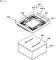
FIG. 1 is a perspective view of a camera device according to the present embodiment. -
FIGS. 2 andFIG.3 are exploded perspective views of a camera device according to the present embodiment. -
FIG. 4 is an exploded perspective view of a camera module according to the present embodiment. -
FIG. 5a is a cross-sectional view taken along line A-A ofFIG. 1 . -
FIGS. 5b and5c are enlarged views of a part ofFIG. 5a . -
FIG. 6 is a cross-sectional view taken along line B-B ofFIG. 1 . -
FIG. 7 is a cross-sectional view taken along line C-C ofFIG. 1 . -
FIG. 8 is a perspective view of a partial configuration of a camera device according to the present embodiment. -
FIG. 9 is a plan view of a partial configuration of a camera device according to the present embodiment. -
FIG. 10a is a bottom view of a partial configuration of a camera device according to the present embodiment. -
FIG. 10b is a perspective view of an elastic member according to the present embodiment. -
FIG. 11 is a bottom perspective view of a partial configuration of a camera device according to the present embodiment. -
FIG. 12 is an exploded perspective view of a partial configuration of the camera device ofFIG. 11 . -
FIG. 13 is a bottom perspective view of a partial configuration of a camera device according to the present embodiment. -
FIG. 14 is a perspective view of a partial configuration of a camera device according to the present embodiment. -
FIG. 15 is a side view of a partial configuration of a camera device according to the present embodiment. -
FIG. 16 is a perspective view illustrating a magnet and a coil of a camera device according to the present embodiment. -
FIG. 17 (a) is a diagram for explaining a yaw driving to one side of a camera module in a camera device according to the present embodiment,FIG. 17 (b) is a diagram for explaining a pitching driving to one side of a camera module, andFIG. 17 (c) is a diagram for explaining the rolling driving to one side of a camera module. -
FIG. 18 (a) is a diagram for explaining a yaw driving to the other side of a camera module in a camera device according to the present embodiment,FIG. 18 (b) is a diagram for explaining a pitching driving to the other side of a camera module, andFIG. 18 (c) is a diagram for explaining the rolling driving of a camera module to the other side. -
FIG. 19 is a diagram for explaining 5-axis correction of a camera device according to the present embodiment. -
FIG. 20 is a perspective view of an optical device according to the present embodiment. -
FIG. 21 is a block diagram of an optical device illustrated inFIG. 20 . - Hereinafter, preferred embodiments of the present invention will be described in detail with reference to the accompanying drawings.
- However, the technical idea of the present invention is not limited to some embodiments to be described, but may be implemented in various forms, and within the scope of the technical idea of the present invention, one or more of the constituent elements may be selectively combined or substituted between embodiments.
- In addition, the terms (comprising technical and scientific terms) used in the embodiments of the present invention, unless explicitly defined and described, can be interpreted as a meaning that can be generally understood by a person skilled in the art, and commonly used terms such as terms defined in the dictionary may be interpreted in consideration of the meaning of the context of the related technology.
- In addition, terms used in the present specification are for describing embodiments and are not intended to limit the present invention.
- In the present specification, the singular form may comprise the plural form unless specifically stated in the phrase, and when described as "at least one (or more than one) of A and B and C", it may comprise one or more of all combinations that can be combined with A, B, and C.
- In addition, in describing the components of the embodiment of the present invention, terms such as first, second, A, B, (a), and (b) may be used. These terms are merely intended to distinguish the components from other components, and the terms do not limit the nature, order or sequence of the components.
- And, when a component is described as being 'connected', 'coupled' or 'interconnected' to another component, the component is not only directly connected, coupled or interconnected to the other component, but may also comprise cases of being 'connected', 'coupled', or 'interconnected' due that another component between that other components.
- In addition, when described as being formed or disposed in "on (above)" or "below (under)" of each component, "on (above)" or "below (under)" means that it comprises not only the case where the two components are directly in contact with, but also the case where one or more other components are formed or disposed between the two components. In addition, when expressed as "on (above)" or "below (under)", the meaning of not only an upward direction but also a downward direction based on one component may be comprised.
- An 'optical axis direction' used hereinafter is defined as 'an optical axis (refer to OA in
FIG. 8 ) direction of a lens and/or an image sensor being coupled to a lens driving device. - The 'vertical direction' used hereinafter may be a direction parallel to the optical axis direction. The vertical direction may correspond to the 'z-axis direction (refer to
FIG. 8 )'. The 'horizontal direction' used below may be a direction perpendicular to the vertical direction. That is, the horizontal direction may be a direction perpendicular to the optical axis. Accordingly, the horizontal direction may comprise an 'x-axis direction' and a 'y-axis direction' (refer toFIG. 8 ). - The 'auto focus function' used hereinafter is defined as a function in which, in order to obtain a clear image of a subject on the image sensor, a lens is moved in an optical axis direction according to the distance of the subject and the distance from the image sensor is adjusted to automatically focus on the subject. Meanwhile, 'auto focus' may correspond to 'AF (Auto Focus)'.
- The 'hand-shake correction function' used hereinafter is defined as a function that moves the lens and/or the image sensor to cancel the vibration (movement) generated in the image sensor by an external force. Meanwhile, 'hand-shake correction' may correspond to 'optical image stabilization (OIS)'.
- 'Yawing' used hereinafter may be a movement in a yaw direction rotating about a y-axis (refer to
FIGS. 17 and18 (a) ). 'Pitching' used hereinafter may be a movement in a pitch direction rotating about an x-axis (refer toFIGS. 17 and18 (b) ). 'Rolling' used hereinafter may be a movement in a roll direction rotating about a z-axis (refer toFIGS. 17 and18 (c) ). - Hereinafter, any one of the "
first substrate 690", "second substrate 50", and "third substrate 230" is referred to as a first substrate, another one is referred to as a second substrate, yet another one is referred to as a third substrate, and the remaining one may be referred to as a fourth substrate. That is, the first, second, and the like described in front of the substrate are only for distinction among the substrates. Furthermore, the use of the first, second, and the like may be applied similarly to configurations other than the substrate. - Hereinafter, the configuration of the camera device will be described with reference to the drawings.
-
FIG.1 is a perspective view of a camera device according to the present embodiment;FIGS. 2 andFIG. 3 are exploded perspective views of a camera device according to the present embodiment;FIG. 4 is an exploded perspective view of a camera module according to the present embodiment;FIG. 5a is a cross-sectional view taken along line A-A ofFIG. 1 ;FIGS. 5b and5c are enlarged views of a part ofFIG. 5a ;FIG. 6 is a cross-sectional view taken along line B-B ofFIG. 1 ;FIG. 7 is a cross-sectional view taken along line C-C ofFIG. 1 ;FIG. 8 is a perspective view of a partial configuration of a camera device according to the present embodiment;FIG. 9 is a plan view of a partial configuration of a camera device according to the present embodiment;FIG. 10a is a bottom view of a partial configuration of a camera device according to the present embodiment;FIG. 10b is a perspective view of an elastic member according to the present embodiment;FIG. 11 is a bottom perspective view of a partial configuration of a camera device according to the present embodiment;FIG. 12 is an exploded perspective view of a partial configuration of the camera device ofFIG. 11 ;FIG. 13 is a bottom perspective view of a partial configuration of a camera device according to the present embodiment;FIG. 14 is a perspective view of a partial configuration of a camera device according to the present embodiment;FIG. 15 is a side view of a partial configuration of a camera device according to the present embodiment;FIG. 16 is a perspective view illustrating a magnet and a coil of a camera device according to the present embodiment;FIG. 17 (a) is a diagram for explaining a yaw driving to one side of a camera module in a camera device according to the present embodiment;FIG. 17 (b) is a diagram for explaining a pitching driving to one side of a camera module;FIG. 17 (c) is a diagram for explaining the rolling driving to one side of a camera module;FIG. 18 (a) is a diagram for explaining a yaw driving to the other side of a camera module in a camera device according to the present embodiment;FIG. 18 (b) is a diagram for explaining a pitching driving to the other side of a camera module;FIG. 18 (c) is a diagram for explaining the rolling driving of a camera module to the other side; andFIG. 19 is a diagram for explaining 5-axis correction of a camera device according to the present embodiment. - The
camera device 10A may comprise a camera module. Thecamera device 10A may comprise a lens driving device. The lens driving device may be a voice coil motor (VCM). The lens driving device may be a lens driving motor. The lens driving device may be a lens driving actuator. The lens driving device may comprise an AF module. The lens driving device may comprise an OIS module. The lens driving device may comprise a focus-tunable lens 630. - The
camera device 10A may comprise a stator. The stator may be a fixed part when the mover moves. The stator may comprise asecond substrate 50. The stator may comprise abase 110. The stator may comprise ahousing 210. - The
camera device 10A may comprise a mover. The mover may be a part moving against the stator. The mover may comprise acamera module 600. The mover may comprise aholder 310. - The
camera device 10A may comprise a driving unit. The driving unit may move the mover against the stator. The driving unit may be disposed above theconnection member 430. The driving unit may comprise a plurality of driving units. The driving unit may comprise: a first driving unit for rotating thecamera module 600 in a first direction with respect to the stator; a second driving unit for rotating thecamera module 600 in a second direction different from the first direction with respect to the stator; a third driving unit for rotating thecamera module 600 in a third direction different from the first and second directions with respect to the stator. The driving unit may comprise: a fourth driving unit for moving the focus of thelens 625 in a fourth direction different from the first to third directions, and a fifth driving unit for moving the focus of thelens 625 in a fifth direction different from the first to fourth directions. The fourth driving unit may move thelens 625 in a fourth direction different from the first to third directions. The fifth driving unit may move thelens 625 in a fifth direction different from the first to fourth directions. At this time, the first direction is a direction to rotate about a first axis perpendicular to the optical axis of theimage sensor 695, the second direction is a direction to rotate about an optical axis and a second axis perpendicular to the first axis, the third direction may be a direction rotating about the optical axis. The fourth direction may be a direction parallel to the first axis, and the fifth direction may be a direction parallel to the second axis. The first direction is a direction in which thecamera module 600 is yawed, the second direction is a direction in which thecamera module 600 is pitched, and the third direction may be a direction in which thecamera module 600 is rolled. - In the present embodiment, when the
camera module 600 is moved by any one or more of the first driving unit, the second driving unit, and the third driving unit, thelens 625 may move together with theimage sensor 695 while being aligned with the optical axis. At this time, the case in which thecamera module 600 moves may be a case in which thecamera module 600 is tilted. In addition, a case in which thecamera module 600 moves may be a case in which thecamera module 600 is rotated. In addition, a case in which thecamera module 600 moves may be a case in which thecamera module 600 moves. - The camera module in which the
lens 625 and theimage sensor 695 are aligned may be tilted about the first axis and the second axis and rotated about the optical axis by the first to third driving units. - Each of the first to third driving units may comprise a coil and a magnet. Each of the fourth and fifth driving units may comprise a coil and a magnet. However, a focus-
tunable lens 630 comprising a fourth driving unit and a fifth driving unit may be provided. That is, the focus-tunable lens 630 may move the focus of thelens 625 along a first axis and a second axis. At this time, the first axis may be an x-axis direction and the second axis may be a y-axis direction. As a modified embodiment, the focus-tunable lens 630 may be tilted about the first axis and the second axis. At this time, the first driving unit and the second driving unit may shift thecamera module 600 along the first axis and the second axis. - The focus-
tunable lens 630 may be tilted about the first axis and the second axis and rotated about an optical axis together with theimage sensor 695 by the first to third driving units. The focus-tunable lens 630 may also be tilted in two axes and rotated in one axis together with thecamera module 600. That is, when thecamera module 600 is tilted in two axes or rotates in one axis, the focus-tunable lens 630 may also move together. The first driving unit may comprise a first magnet 321 and afirst coil 221. The second driving unit may comprise a first magnet 321 and asecond coil 222. The third driving unit may comprise a second magnet 322 and athird coil 223. As a modified embodiment, the second driving unit may comprise a third magnet separate from the first magnet 321 and the second magnet 322. - The
camera device 10A may comprise abase 110. The base 110 may be disposed on thesecond substrate 50. The base 110 may be disposed on thesecond substrate 50. The base 110 may be disposed on an upper surface of thesecond substrate 50. The base 110 may be disposed between thehousing 210 and thesecond substrate 50. The base 110 may be coupled to theside plate 520 of thecover 500. - The base 110 may comprise a
hole 111. Thehole 111 may be a hollow hole. Thehole 111 may be an opening. Thehole 111 may be formed to penetrate through the base 110 in an optical axis direction. The base 110 may comprise agroove 112. Thegroove 112 may be formed on an upper surface of thebase 110. Thegroove 112 may be formed at the periphery of thehole 111. Anelastic member 120 may be disposed in thegroove 112. The depth of thegroove 112 may be lower than the height of the protruded part 121-1 of theelastic member 120. Through this, the protruded part 121-1 of theelastic member 120 disposed in thegroove 112 may be protruded further than the upper surface of thebase 110. - The base 110 may comprise a
guide wall 114. Theguide wall 114 may be formed to be protruded from an upper surface of thebase 110. Theguide wall 114 may be formed to be spaced apart from the outer periphery of thebase 110. A distance between theguide wall 114 and the outer periphery of the base 110 may correspond to the thickness of theside plate 520 of thecover 500. That is, theside plate 520 of thecover 500 may be disposed on an upper surface of the base 110 between theguide wall 114 and the outer periphery of thebase 110. Theguide wall 114 may serve as an assembly guide for theside plate 520 of thecover 500, while supporting the inner surface of theside plate 520 of the assembledcover 500. Furthermore, theside plate 520 of thecover 500 may be fixed to an upper surface of theguide wall 114 and/or the base 110 through an adhesive. - The
camera device 10A may comprise anelastic member 120. Theelastic member 120 may be disposed on thebase 110. Theelastic member 120 may elastically support thecamera module 600. Theelastic member 120 may be disposed between thecamera module 600 and thebase 110. Theelastic member 120 may have elasticity at least in part. Theelastic member 120 may be formed of metal. Theelastic member 120 may comprise a leaf spring. - In order to disperse the stress concentration on the
first substrate 690 due to the contact support structure at the center of the lower surface of thecamera module 600, anelastic member 120 that is a shock-relieving spring structure may be applied to the contact support structure. That is, theelastic member 120 may relieve stress concentration at a specific point of thefirst substrate 690 by the preload structure through the upperelastic member 410. In the present embodiment, a shock-relieving spring structure is applied to the support structure of thecamera module 600, and thereby, in the case of a drop impact, the stress concentration applied to thefirst substrate 690 is dispersed so that there is an effect of preventing damage to theimage sensor 695. - The
elastic member 120 may comprise aninner portion 121. Theinner portion 121 may be disposed inside anouter portion 122. Theinner portion 121 may comprise a protruded part 1211. The protruded part 1211 may provide a pivot center for a pivot movement of thecamera module 600. The protruded part 1211 may be in contact with thecamera module 600. The protruded part 1211 may in contact with a lower surface of thecamera module 600. The protruded part 1211 may in contact with thefirst substrate 690. The protruded part 1211 may elastically support thecamera module 600. An upper end of the protruded part 1211 may be formed to be round. The protruded part 1211 may comprise a portion having a curvature. - The
elastic member 120 may comprise anouter portion 122. Theouter portion 122 may be disposed on thebase 110. Theouter portion 122 may be disposed in thegroove 112 of thebase 110. Theouter portion 122 may be fixed to thebase 110 by an adhesive. Theouter portion 122 may have a rectangular frame shape. - The
elastic member 120 may comprise aconnection part 123. Theconnection part 123 may connect theinner portion 121 and theouter portion 122. Theconnection part 123 may have elasticity. Theconnection part 123 may elastically connect theouter portion 122 which is a fixed part and theinner portion 121 which is a movable part. Theconnection part 123 may comprise a bending or bent part. Theconnection part 123 may comprise a shape being rounded. - The
camera device 10A may comprise ahousing 210. Thehousing 210 may be disposed on thebase 110. Thehousing 210 may be disposed on an upper surface of thebase 110. Thehousing 210 may be disposed below theholder 310. Thehousing 210 may accommodate a part of theholder 310 and thecamera module 600 at an inner side thereof. Thehousing 210 may comprise a plurality of sidewalls. Thehousing 210 may comprise four sidewalls. Thehousing 210 may comprise first to fourth sidewalls. Thehousing 210 may comprise a first sidewall and a second sidewall disposed opposite to each other, and a third sidewall and a fourth sidewall disposed opposite to each other between the first sidewall and the second sidewall. Acoil 220 may be disposed on each of the first to fourth sidewalls of thehousing 210. - The
housing 210 may comprise afirst groove 211. Thefirst groove 211 may be formed in a sidewall of thehousing 210. Acoil 220 may be disposed in thefirst groove 211. That is, thefirst groove 211 may be an 'accommodating groove' for accommodating thecoil 220. Thefirst groove 211 may be formed as the upper surface of thehousing 210 is being recessed. As a modified embodiment, thefirst groove 211 may be provided in the form of a hole penetrating the sidewall of thehousing 210 in a direction perpendicular to the optical axis. Thefirst groove 211 may comprise a plurality of grooves. Thefirst groove 211 may be formed in each of the four sidewalls of thehousing 210. - The
housing 210 may comprise asecond groove 212. Thesecond groove 212 may be formed in a sidewall of thehousing 210. Theconnection member 430 may pass through the space being formed through thesecond groove 212. That is, thesecond groove 212 may be an 'avoiding groove' for avoiding interference with theconnection member 430. Thesecond groove 212 may be formed as a lower surface of thehousing 210 is being recessed. Thesecond groove 212 may comprise a plurality of grooves. Thesecond groove 212 may be formed in each of one sidewall and the other sidewall of thehousing 210. - The
housing 210 may comprise a hole. The hole may be formed to penetrate through thehousing 210 in a direction parallel to the optical axis. Awire 420 may be disposed in the hole. The hole may be formed with a diameter that does not interfere with thewire 420. The hole may be formed in a corner portion of thehousing 210. The hole may comprise a plurality of holes. A hole may be formed in each of the four corner portions of thehousing 210. However, as a modified embodiment, the hole may be formed as a groove with a closed bottom. In this case, the lower end of thewire 420 may be fixed to thehousing 210. - The
camera device 10A may comprise acoil 220. Thecoil 220 may be disposed in thehousing 210. Thecoil 220 may face themagnet 320. Thecoil 220 may be coupled to an inner surface of athird substrate 230. Thecoil 220 may be electrically connected to thethird substrate 230. When a current is applied to thecoil 220, an electric field may be formed around thecoil 220. When a current is applied to thecoil 220, one of thecoil 220 and themagnet 320 may move relative to the other through electromagnetic interaction between thecoil 220 and themagnet 320. In the present embodiment, when a current is applied to thecoil 220, themagnet 320 may move. However, in the modified embodiment, the positions of thecoil 220 and themagnet 320 may be disposed opposite to each other. - The
coil 220 may comprise afirst coil 221. Thefirst coil 221 may face the first magnet 321. Thefirst coil 221 may be electrically separated from thesecond coil 222 and thethird coil 223. Thefirst coil 221 may receive current separately from thesecond coil 222 and thethird coil 223. Thefirst coil 221 may be controlled separately from thesecond coil 222 and thethird coil 223. When a current is applied to thefirst coil 221, no current may be applied to thesecond coil 222 and thethird coil 223. In addition, when a current is applied to thefirst coil 221, a current may be applied to thesecond coil 222 and thethird coil 223. When no current is applied to thefirst coil 221, current may be applied to thesecond coil 222 and thethird coil 223. Of course, no current may be applied to all of the first tothird coils third coils third coils third coils first coil 221 may rotate thecamera module 600 about a first axis perpendicular to the optical axis through interaction with themagnet 320. Thefirst coil 221 may tilt thecamera module 600 about a first axis perpendicular to the optical axis through interaction with themagnet 320. Thecamera module 600 may be pivotally driven about a first axis perpendicular to the optical axis. At this time, the first axis may be an x-axis. - As illustrated in
FIG. 17 (b) , thefirst coil 221 may rotate (refer to b inFIG. 17 (b) ) thecamera module 600 to one side about the x-axis through interaction with themagnet 320. In more detail, when a forward current is applied to the first-first coil 221-1, an electromagnetic interaction force b1 is generated upwardly between the first-first coil 221-1 and the first-first magnet 321-1, and when a forward current is applied to the first-second coil 221-1, an electromagnetic interaction force b2 is generated downward between the first-second coil 221-1 and the first-second magnet 321-2, so that thecamera module 600 may rotate (b) to one side about the x-axis. However, the first-first coil 221-1 and the first-second coil 221-1 are not limited to the same direction current being applied, and in a modified embodiment, currents in different directions can be applied. In addition, reverse currents may be applied to the first-first coil 221-1 and the first-second coil 221-1. - As illustrated in
FIG. 18 (b) , thefirst coil 221 may rotate thecamera module 600 to the other side about the x-axis through interaction with the magnet 320 (refer to e inFIG. 18 (b) ). In more detail, when a reverse current is applied to the first-first coil 221-1, an electromagnetic interaction force e1 is generated downward between the first-first coil 221-1 and the first-first magnet 321-1, and when a current is applied upwardly to the first-second coil 221-1, an electromagnetic interaction force e2 is generated upwardly between the first-second coil 221-1 and the first-second magnet 321-2, so that thecamera module 600 can be rotated (e) to the other side about the x-axis. - The
first coil 221 may comprise a plurality of coils. Thefirst coil 221 may comprise a first-first coil 221-1 and a first-second coil 221-1. The first-first coil 221-1 may face the first-first magnet 321-1. The first-second coil 221-1 may face the first-second magnet 321-2. The first-first coil 221-1 may be disposed between the second-first coil 222-1 and the second-second coil 222-2. The first-second coil 221-1 may be disposed between the second-third coil 222-3 and the second-second coil 222-4. The first-first coil 221-1 and the first-second coil 221-1 may be electrically connected. Through this, the first-first coil 221-1 and the first-second coil 221-1 can be integrally controlled. However, as another example, the first-first coil 221-1 and the first-second coil 221-1 may be electrically separated. The first-first coil 221-1 and the first-second coil 221-1 may receive current individually. In this case, the first-first coil 221-1 and the first-second coil 221-1 may be individually controlled. That is, the direction and amount of current applied to each of the first-first coil 221-1 and the first-second coil 221-1 may be individually controlled. - The
coil 220 may comprise asecond coil 222. Thesecond coil 222 may face the first magnet 321. Thesecond coil 222 may be electrically separated from thefirst coil 221. Thesecond coil 222 and thefirst coil 221 may receive current individually. Thesecond coil 222 and thefirst coil 221 may be individually controlled. Thesecond coil 222 may rotate thecamera module 600 about an optical axis and a second axis perpendicular to the first axis through interaction with themagnet 320. Thesecond coil 222 may tilt thecamera module 600 about an optical axis and a second axis perpendicular to the first axis through interaction with themagnet 320. Thecamera module 600 may be pivotally driven about an optical axis and a second axis perpendicular to the first axis. At this time, the second axis may be a y-axis. - As illustrated in
FIG. 17 (a) , thesecond coil 222 may rotate thecamera module 600 to one side about a y-axis through interaction with the magnet 320 (refer to a inFIG. 17 (a) ). In more detail, when a forward current is applied to the second-first coil 222-1, an electromagnetic interaction force a1 is generated upwardly between the second-first coil 222-1 and the first-first magnet 321-1; when a forward current is applied to the second-third coil 222-3, an electromagnetic interaction force a1 is generated upwardly between the second-third coil 222-3 and the first-second magnet 321-2; when a reverse current is applied to the second-second coil 222-2, an electromagnetic interaction force a2 is generated downward between the second-second coil 222-2 and the first-first magnet 321-1; and when a reverse current is applied to the second-fourth coil 222-4, an electromagnetic interaction force a2 is generated downward between the second-fourth coil 222-4 and the first-second magnet 321-2. Thecamera module 600 may rotate (a) to one side about a y-axis. The electromagnetic interaction force a1 between the second-first coil 222-1 and the first-first magnet 321-1 and the electromagnetic interaction force a1 between the second-third coil 222-3 and the first-second magnet 321-2 faces the same direction; the electromagnetic interaction force a2 between the second-second coil 222-2 and the first-first magnet 321-1 and the electromagnetic interaction force a2 between the second-second coil 222-4 and the first-second magnet 321-2 are directed in the same direction; however, the electromagnetic interaction force a1 between the second-first coil 222-1 and the first-first magnet 321-1 and the electromagnetic interaction force a2 between the second-second coil 222-2 and the first-first magnet 321-1 may face different directions. For example, the electromagnetic interaction force a1 between the second-first coil 222-1 and the first-first magnet 321-1 and the electromagnetic interaction force a1 between the second-third coil 222-3 and the first-second magnet 321-2 is directed upward, and the electromagnetic interaction force a2 between the second-second coil 222-2 and the first-first magnet 321-1 and the electromagnetic force a2 between the second-second coil 222-4 and the first-second magnet 321-2 may be directed downward. Although it has been described that currents in different directions are applied to the second-first coil 222-1 and the second-second coil 222-2, in a modified embodiment, the winding directions of the coils are disposed opposite to each other, and currents in the same direction can be applied. - As illustrated in
FIG. 17 (a) , thesecond coil 222 may rotate thecamera module 600 to the other side about the y-axis through interaction with the magnet 320 (refer to d inFIG. 17 (a) ). In more detail, when a reverse current is applied to the second-first coil 222-1, an electromagnetic interaction force d1 is generated downward between the second-first coil 222-1 and the first-first magnet 321-1; when a reverse current is applied to the second-third coil 222-3, an electromagnetic interaction force d1 is generated downwardly between the second-third coil 222-3 and the first-second magnet 321-2; when a forward current is applied to the second-second coil 222-2, an electromagnetic interaction force d2 is generated upwardly between the second-second coil 222-2 and the first-first magnet 321-1; and when a forward current is applied to the second-fourth coil 222-4, an electromagnetic interaction force d2 is generated upwardly between the second-fourth coil 222-4 and the first-second magnet 321-2. Thecamera module 600 may rotate (d) to the other side about the y-axis. - The
second coil 222 may comprise a plurality of coils. Thesecond coil 222 may comprise second-first to second-fourth coils 222-1, 222-2, 222-3, and 222-4. The second-first coil 222-1 may face the first-first magnet 321-1. The second-first coil 222-1 may be disposed at one side of the first-first coil 221-1. The second-second coil 222-2 may face the first-first magnet 321-1. The second-second coil 222-2 may be disposed at the other side of the first-first coil 221-1. The second-third coil 222-3 may face the first-second magnet 321-2. The second-third coil 222-3 may be disposed at one side of the first-second coil 221-1. The second-fourth coil 222-4 may face the first-second magnet 321-2. The second-fourth coil 222-4 may be disposed on the other side of the first-second coil 221-1. - The second-first to second-fourth coils 222-1, 222-2, 222-3, and 222-4 may be electrically connected. Through this, the second-first to second-fourth coils 222-1, 222-2, 222-3, and 222-4 may be integrally controlled. However, as another example, all of the second-first to second-fourth coils 222-1, 222-2, 222-3, and 222-4 may be electrically separated. In this case, the second-first to second-fourth coils 222-1, 222-2, 222-3, and 222-4 may be individually controlled. That is, the direction and amount of current applied to each of the second-first to second-fourth coils 222-1, 222-2, 222-3, and 222-4 may be individually controlled. As another example, the second-first coil 222-1 and the second-third coil 222-3 are electrically connected; the second-second coil 222-2 and the second-fourth coil 222-4 are electrically connected; and the second-first coil 222-1 and the second-second coil 222-2 may be electrically separated.
- The
coil 220 may comprise athird coil 223. Thethird coil 223 may face the second magnet 322. Thethird coil 223 may be electrically separated from thefirst coil 221 and thesecond coil 222. Thethird coil 223 may receive current separately from any one or more of thefirst coil 221 and thesecond coil 222. Thethird coil 223 may be individually controlled from any one or more of thefirst coil 221 and thesecond coil 222. - As illustrated in
FIG. 17 (c) , thethird coil 223 may rotate thecamera module 600 to one side about an optical axis through interaction with the magnet 320 (refer to c inFIG. 17 (c) ). In more detail, when a forward current is applied to the third-first coil 223-1, an electromagnetic interaction force c1 in a first direction is generated between the third-first coil 223-1 and the second-first magnet 322-1; when a forward current is applied to the third-second coil 223-2, an electromagnetic interaction force c2 is generated in a second direction between the third-second coil 223-2 and the second-second magnet 322-2, so that thecamera module 600 may rotate (c) about the z-axis to one side. At this time, the first direction and the second direction are tangential directions of a circle centered about the optical axis, respectively, and may be symmetrical with respect to the optical axis. Although it has been described that the forward current is applied to each of the third-first coil 223-1 and the third-second coil 223-2, in a modified embodiment, currents in different directions may be applied to the third-first coil 223-1 and the third-second coil 223-2. At this time, a necessary electromagnetic interaction force can be induced through the disposement direction of the third-first coil 223-1 and the third-second coil 223-2. - As illustrated in
FIG. 17 (c) , thethird coil 223 may rotate thecamera module 600 to the other side about the optical axis through interaction with the magnet 320 (refer to f inFIG. 17 (c) ). In more detail, when a reverse current is applied to the third-first coil 223-1, an electromagnetic interaction force f1 is generated in a third direction between the third-first coil 223-1 and the second-first magnet 322-1, and when the reverse current is applied to the third-second coil 223-2, the electromagnetic interaction force f2 is generated in in a fourth direction between the third-second coil 223-2 and the second-second magnet 322-2, so that thecamera module 600 may rotate (f) to the other side about a z-axis. At this time, the third and fourth directions are tangential directions of a circle centered on an optical axis, respectively, and may be symmetrical with respect to the optical axis. In addition, the third direction is opposite to the first direction and the fourth direction may be opposite to the second direction. - The
third coil 223 may comprise a plurality of coils. Thethird coil 223 may comprise a third-first coil 223-1 and third-second coil 223-2. The third-first coil 223-1 may face the second-first magnet 322-1. The third-second coil 223-2 may face the second-second magnet 322-2. The third-first coil 223-1 and the third-second coil 223-2 may be electrically connected to each other. Through this, the third-first coil 223-1 and third-second coil 223-2 may be integrally controlled. However, as another example, the third-first coil 223-1 and third-second coil 223-2 may be electrically separated. In this case, the third-first coil 223-1 and third-second coil 223-2 may be individually controlled. That is, the direction and amount of current applied to each of the third-first coil 223-1 and third-second coil 223-2 may be individually controlled. - The
camera device 10A may comprise athird substrate 230. Thethird substrate 230 may be disposed on an outer surface of thehousing 210. Thethird substrate 230 may connect thesecond substrate 50 and thecoil 220. Acoil 220 may be coupled to an inner surface of thethird substrate 230. Asensor 440 may be coupled to an inner surface of thethird substrate 230. A lower end of thethird substrate 230 may be coupled to thesecond substrate 50. Thethird substrate 230 may be flexible. Thethird substrate 230 may comprise a flexible printed circuit board (FPCB). - The
third substrate 230 may comprise a plurality of substrates. Thethird substrate 230 may comprise a first-first substrate 230-1 and a first-second substrate 230-2. The first-first substrate 230-1 may be disposed on the first sidewall and the third sidewall of thehousing 210. The first-second substrate 230-2 may be disposed on the second sidewall and the fourth sidewall of thehousing 210. The first-first substrate 230-1 and the first-second substrate 230-2 may have corresponding shapes. The first-first substrate 230-1 and the first-second substrate 230-2 may be symmetrically disposed with respect to the central axis of thehousing 210. Four coils may be coupled to each of the first-first substrate 230-1 and the first-second substrate 230-2. Two sensors may be coupled to each of the first-first substrate 230-1 and the first-second substrate 230-2. - The
third substrate 230 may comprise a terminal 231. The terminal 231 may be formed at a lower end of thethird substrate 230. The terminal 231 may be coupled to the terminal 50a of thesecond substrate 50 by soldering. The terminal 231 may comprise a plurality of terminals. - The
third substrate 230 may comprise abent portion 232. Thethird substrate 230 may comprise a flat plate portion disposed on an outer surface of thehousing 210 and abent portion 232 connecting the two flat plate portions. Thebent portion 232 may be formed to be round. Thethird substrate 230 may have flexibility in thebent portion 232. - The
camera device 10A may comprise aholder 310. At least a portion of theholder 310 may be disposed inside thehousing 210. A portion of theholder 310 may be disposed above thehousing 210. Theholder 310 may be coupled to thecamera module 600. Thecamera module 600 may be disposed inside of theholder 310. Amagnet 320 may be disposed in theholder 310. Theholder 310 may comprise an upper plate and a plurality of sidewalls being extended from the upper plate. A plurality of sidewalls of theholder 310 may be extended along an outer periphery surface of thecamera module 600 from the upper plate. The sidewall of theholder 310 may comprise first to fourth sidewalls corresponding to the sidewall of thehousing 210. - The
holder 310 may comprise ahole 311. Thehole 311 may be a hollow hole. Thehole 311 may be an opening. Thehole 311 may be formed to penetrating through theholder 310 in an optical axis direction. Acamera module 600 may be disposed in thehole 311. Thehole 311 may be formed in a size corresponding to thecamera module 600. - The
holder 310 may comprise aprotrusion 312. Theprotrusion 312 may be formed on an upper surface of theholder 310. An upperelastic member 410 may be coupled to theprotrusion 312. Theprotrusion 312 may be formed by being protruded from an upper surface of the upper plate of theholder 310. Theprotrusion 312 may be formed between corners of the upper plate of theholder 310. Theprotrusion 312 may comprise a plurality of protrusions. The number of theprotrusions 312 may be formed to correspond to the number of thefirst coupling parts 411 of the upperelastic member 410. Theprotrusion 312 may comprise four protrusions. - The
holder 310 may comprise astopper 313. Thestopper 313 may be formed by being protruded from an upper surface of theholder 310. Thestopper 313 may limit the upward movement of theholder 310. Thestopper 313 may be an upper stopper. Thestopper 313 may be overlapped with theupper plate 510 of thecover 500 in a direction parallel to the optical axis. Thestopper 313 may comprise a plurality of protrusions. Thestopper 313 may comprise eight protrusions. - The
holder 310 may comprise afirst hole 314. Thefirst hole 314 may be formed in a sidewall of theholder 310. Amagnet 320 may be disposed in thefirst hole 314. Thefirst hole 314 may be a magnet accommodating hole. Thefirst hole 314 may be formed in a size and shape corresponding to themagnet 320. Thefirst hole 314 may comprise a plurality of holes. The number offirst holes 314 may correspond to the number ofmagnets 320. Thefirst hole 314 may comprise four holes. - The
holder 310 may comprise asecond hole 315. Thesecond hole 315 may be formed to penetrate through theholder 310 in a direction parallel to the optical axis. Thesecond hole 315 may be formed at a corner of the upper plate of theholder 310. Thewire 420 may pass through thesecond hole 315. Thesecond hole 315 may be formed to have a larger diameter than thewire 420 so as not to interfere with thewire 420. Thesecond hole 315 may comprise a plurality of holes. The number ofsecond holes 315 may correspond to the number ofwires 420. Thesecond hole 315 may comprise four holes. - The
camera device 10A may comprise amagnet 320. Themagnet 320 may be disposed on an outer periphery surface of thecamera module 600. Themagnet 320 may face thecoil 220. Themagnet 320 may be disposed to face thecoil 220. Themagnet 320 may electromagnetically interact with thecoil 220. When a current is applied to thecoil 220, themagnet 320 may move. Themagnet 320 may be a flat magnet having a flat plate shape. Themagnet 320 may comprise a plurality of magnets. Themagnet 320 may comprise four magnets. - The
magnet 320 may comprise a first magnet 321. The first magnet 321 may be disposed on each of the first side surface and the second side surface of thecamera module 600. The polarity of the upper and lower portions of the surface of the first magnet 321 facing thecoil 220 may be different from each other. The first magnet 321 may be a single magnet having two poles. However, as a modified embodiment, the first magnet 321 may be a bipolar magnetized magnet in which two single magnets having two poles are superimposed. An upper portion of the first magnet 321 may be an N pole and a lower portion may be an S pole. However, in a modified embodiment, an upper portion of the first magnet 321 may be an S pole and a lower portion may be an N pole. The first magnet 321 may face thefirst coil 221 and thesecond coil 222. The width of the first magnet 321 in the horizontal direction may correspond to the sum of the width of thefirst coil 221 and the width of thesecond coil 222. - The first magnet 321 may comprise a first-first magnet 321-1 and a first-second magnet 321-2. The first-first magnet 321-1 may be disposed on the first side surface of the
camera module 600. The first-second magnet 321-2 may be disposed on the second side surface of thecamera module 600. - The
magnet 320 may comprise a second magnet 322. The second magnet 322 may be disposed on each of the third side surface and the fourth side surface of thecamera module 600. The second magnet 322 may have different polarities of the both side portions of the surface facing thecoil 220. - The second magnet 322 may be a single magnet having two poles. However, as a modified embodiment, the second magnet 322 may be a bipolar magnetized magnet in which two single magnets having two poles are superimposed. One side portion of the second magnet 322 may be an N pole and the other side portion may be an S pole. However, in a modified embodiment, one side portion of the second magnet 322 may be an S pole and the other side portion may be an N pole. At this time, one side portion may be a portion located on a left side of the second magnet 322, and the other side portion may be a portion located at a right side of the second magnet 322. The second magnet 322 may face the
third coil 223. The width of the second magnet 322 in the horizontal direction may be greater than the width of thethird coil 223. - The second magnet 322 may comprise a second-first magnet 322-1 and a second-second magnet 322-2. The second-first magnet 322-1 may be disposed on a third side surface of the
camera module 600. The second-second magnet 322-2 may be disposed on a fourth side surface of thecamera module 600. - The
camera device 10A may comprise an upperelastic member 410. A part of the upperelastic member 410 may be coupled to theholder 310. The upperelastic member 410 may be fixed to theprotrusion 312 of theholder 310 by an adhesive. The upperelastic member 410 may connect theholder 310 and thewire 420. The upperelastic member 410 may have elasticity at least in part. The upperelastic member 410 may comprise a leaf spring. - As shown in
FIGS. 17 and18 , in the present embodiment, a contact support structure may be applied to the center of a lower surface of thecamera module 600. At this time, the upperelastic member 410 being provided with a leaf spring is formed to be offset-banded after assembly so as to form a preload structure in which theentire camera module 600 receives a force in the direction of thebase 110, thereby preventing posture difference sagging due to gravity. The present embodiment is a structure in which the upperelastic member 410 is offset-banded to apply a preload in a state of product assembly, so in the present embodiment, even if a change in the direction of gravity occurs, the preload, which is the normal drag, is sufficiently large compared to the weight of thecamera module 600 therefore the sagging of thecamera module 600 according to the posture difference may not occur. Referring toFIG. 15 , an offset-bend structure for generating a height difference (refer to a inFIG. 15 ) existing between thefirst coupling part 411 and thesecond coupling part 412 of the upperelastic member 410 can be confirmed. In the present embodiment, the offset bend shape of the upperelastic member 410 may be maintained in all postures in which thecamera module 600 photographs above, thecamera module 600 photographs below, and thecamera module 600 photographs side direction. In other words, the offset bend shape of the upperelastic member 410 may be maintained in all postures in which thelens 625 of thecamera module 600 is disposed above animage sensor 695, thelens 625 of thecamera module 600 is disposed below theimage sensor 695, and the center of thelens 625 of thecamera module 600 and the center of theimage sensor 695 are disposed at the same height. Through this, the posture difference sagging of thecamera module 600 may be prevented. By the preload of the upperelastic member 410, a frictional force F acts between thecamera module 600 and the protruded part 1211 of theelastic member 120, and through this, posture difference sagging can be prevented. However, the amount of offset bending of the upperelastic member 410 may be changed according to the posture. - The upper
elastic member 410 may comprise afirst coupling part 411. Thefirst coupling part 411 may be coupled to theholder 310. Thefirst coupling part 411 may be coupled to an upper surface of theprotrusion 312 of theholder 310 by an adhesive. Thefirst coupling part 411 may be formed to have a wider width than the width of theconnection part 413. - The upper
elastic member 410 may comprise asecond coupling part 412. Thesecond coupling part 412 may be connected to thewire 420. Thesecond coupling part 412 may be coupled to thewire 420. Thesecond coupling part 412 may be coupled to thewire 420 by soldering. Thesecond coupling part 412 may comprise a hole through which thewire 420 passes. - The upper
elastic member 410 may comprise aconnection part 413. Theconnection part 413 may connect thefirst coupling part 411 and thesecond coupling part 412. Theconnection part 413 may have elasticity. Theconnection part 413 may elastically connect thefirst coupling part 411 and thesecond coupling part 412. Theconnection part 413 may be integrally formed with thefirst coupling part 411 and thesecond coupling part 412. - The
camera device 10A may comprise awire 420. Thewire 420 may connect theelastic member 120 and thehousing 210 or theelastic member 120 and thebase 110. An upper end portion of thewire 420 may be coupled to thesecond coupling part 412 of the upperelastic member 410. A lower end portion of thewire 420 may be coupled to thebase 110. In a modified embodiment, a lower end portion of thewire 420 may be coupled to a lower portion of thehousing 210. In a modified embodiment, a lower end portion of thewire 420 may be coupled to thesecond substrate 50. Thewire 420 may pass through the hole of thesecond coupling part 412 of the upperelastic member 410, thesecond hole 315 of theholder 310, and the hole of thehousing 210. Thewire 420 may comprise a wire spring. - In the present embodiment, a rotational force is generated about the X, Y, and Z axes through the electromagnetic interaction of the
coil 220 and themagnet 320, and the rigidity against 3-axis rotation is decreased by disposing the upperelastic member 410 being provided as a leaf spring and thewire 420 being provided as a wire spring to be perpendicular to each other, thereby enabling the movement in Yaw, Pitch, and Roll modes. That is, since the rigidity is lowered through thewire 420, in the present embodiment, the current being consumed for 3-axis rotation driving can be reduced. - The
wire 420 may comprise a plurality of wires. Thewire 420 may comprise four wires. Thewire 420 may comprise first to fourth wires. The first to fourth wires may be respectively disposed at four corners of theholder 310. - The
camera device 10A may comprise aconnection member 430. Theconnection member 430 may be coupled to thefirst substrate 690. Theconnection member 430 may connect thefirst substrate 690 and thesecond substrate 50. Theconnection member 430 may electrically connect theimage sensor 695 and thesecond substrate 50. Theconnection member 430 may elastically support the movement of thecamera module 600. A part of theconnection member 430 may move integrally with thecamera module 600. Theconnection member 430 may be flexible. Theconnection member 430 may comprise a plurality of springs. Theconnection member 430 may comprise a plurality of elastic members. Theconnection member 430 may comprise a flexible printed circuit board (FPCB). - The
connection member 430 may comprise afirst coupling part 431. Thefirst coupling part 431 may be an inner portion. Thefirst coupling part 431 may be coupled to thefirst substrate 690. Thefirst coupling part 431 may move integrally with thecamera module 600. Thefirst coupling part 431 may comprise a substrate. Thefirst coupling part 431 may comprise a first terminal 431-1. The first terminal 431-1 may be connected to the terminal 691 being disposed on a lower surface of thefirst substrate 690. Thefirst coupling part 431 may comprise a hole. The hole of thefirst coupling part 431 may be a hollow hole. The protruded part 1211 of theelastic member 120 may be disposed in the hole of thefirst coupling part 431. Thefirst coupling part 431 may be disposed in a rigid PCB 432-2 of thesecond coupling part 432. Thefirst coupling part 431 may be connected to theterminal 691 of thefirst substrate 690. The first terminal 431-1 may be connected to theterminal 691 of thefirst substrate 690. - The
connection member 430 may comprise asecond coupling part 432. Thesecond coupling part 432 may be an outer portion. Thesecond coupling part 432 may be fixed to thebase 110. Thesecond coupling part 432 may comprise a substrate. Thesecond coupling part 432 may be coupled to thesecond substrate 50. Thesecond coupling part 432 may comprise a second terminal 432-1. The second terminal 432-1 of thesecond coupling part 432 may be coupled to the terminal of thesecond substrate 50 by soldering. Thesecond coupling part 432 may be connected to a terminal of thesecond substrate 50. The second terminal 432-1 may be connected to the terminal of thesecond substrate 50. - The
connection member 430 may comprise a rigid printed circuit board (RPCB) 432-2 and a flexible printed circuit board (FPCB) 432-3. The RPCB 432-2 may be a rigid PCB 432-2. The FPCB 432-3 may be a flexible PCB 432-3. However, the rigid PCB 432-2 and the flexible PCB 432-3 may be formed separately from the substrate of thesecond coupling part 432. A rigid PCB 432-2 can be coupled with a plurality of springs. The flexible PCB 432-3 is connected to the rigid PCB 432-2 and may comprise a second terminal 432-1. In another embodiment, RPCB 432-2 and FPCB 432-3 may be formed as a substrate. - The
connection member 430 may comprise aconnection part 433. Theconnection part 433 may connect thefirst coupling part 431 and thesecond coupling part 432. Theconnection part 433 may be bent at least in part. Theconnection part 433 may be flexible. Theconnection part 433 may be flexible. Theconnection part 433 may have elasticity. Theconnection part 433 may elastically connect thefirst coupling part 431 and thesecond coupling part 432. - One end of the
connection part 433 may be coupled to thefirst coupling part 431. One end of theconnection part 433 may be coupled to theterminal 691 of thefirst substrate 690. One end of theconnection part 433 may be soldered to theterminal 691 of thefirst substrate 690. One end of theconnection part 433 may be soldered to theterminal 691 of thefirst substrate 690. One end of theconnection part 433 may be electrically connected to theterminal 691 of thefirst substrate 690. - The other end of the
connection part 433 may be coupled to thesecond coupling part 432. The other end of theconnection part 433 may be coupled to the RPCB 432-2. The other end of theconnection part 433 may be soldered to the RPCB 432-2. The other end of theconnection part 433 may be soldered to the RPCB 432-2. The other end of theconnection part 433 may be electrically connected to the RPCB 432-2 and the FPCB 432-3. Through this, the other end of theconnection part 433 may be electrically connected to thesecond substrate 50. - The
connection part 433 may comprise a plurality of springs spaced apart from each other. The plurality of springs may comprise 28 springs. Each of the plurality of springs may comprise a shape that is bent at least twice. Each of the plurality of springs may comprise a shape that is bent three times. Each of the plurality of springs may comprise a shape bent at 90 degrees. Each of the plurality of springs may comprise a shape that is bent three or more times by 90 degrees. In the present embodiment, theimage sensor 695 and thesecond substrate 50 may be electrically conducted through a plurality of springs. In the present embodiment, a plurality of springs are used so that the reaction force generated when thecamera module 600 is rolled is reduced compared to when a PCB is used, so the current consumption can also be reduced. - The
connection part 433 may comprise a plurality of conducting wires having an elastic force. Theconnection part 433 has elasticity and may be formed of a material to which current is supplied. Theconnection part 433 may be divided into four parts or regions comprising corresponding shapes. One part of the four parts may comprise seven springs. - In the present embodiment, a metal spring having a thickness of 30 µm and a width of 30 µm may be applied to each of the plurality of springs. Through this, not only the electrical connection of 20 to 30
image sensors 695 but also implementation of module-tilt OIS module capable of 3-axis hand-shake compensation that can drive X-tilt, Y-tilt, and Z-rotation become possible. - In the present embodiment, it is possible to reduce the dispersion of the rigidity of the spring compared to the PCB type by applying the metal spring of the etching method.
- The
camera device 10A may comprise asensor 440. Thesensor 440 may be disposed on an inner surface of thethird substrate 230. Thesensor 440 may comprise a Hall sensor (Hall IC). Thesensor 440 may detect a magnetic force of themagnet 320. The movement of thecamera module 600 may be detected in real time through the magnetic force of themagnet 320 detected by thesensor 440. Through this, OIS feedback control may be possible. - The
sensor 440 may comprise a plurality of sensors. Thesensor 440 may comprise four sensors. All of the yawing, pitching, and rolling of thecamera module 600 may be detected through the four sensors. Thesensor 440 may comprise first to fourth sensors. The first sensor and the second sensor face the first-first magnet 321-1, the third sensor faces the second-first magnet 322-1, and the fourth sensor may face the first-second magnet 321-2. - The
sensor 440 may comprise a first Hall sensor that detects the movement amount and/or displacement of themagnet 320 in an x-axis direction. Thesensor 440 may comprise a second Hall sensor that detects the movement amount and/or displacement of themagnet 320 in a y-axis direction. Thesensor 440 may comprise a third Hall sensor that detects the movement amount and/or displacement of themagnet 320 in a z-axis direction. Yawing, pitching, and rolling of thecamera module 600 may be detected through any two or more of the first Hall sensor, the second Hall sensor, and the third Hall sensor. - The
camera device 10A may comprise acover 500. Thecover 500 may comprise a 'cover can'. Thecover 500 may be disposed to surround theholder 310 and thehousing 210. Thecover 500 may be coupled to thebase 110. Thecover 500 may accommodate thecamera module 600 therein. Thecover 500 may form an outer appearance of thecamera device 10A. Thecover 500 may have a hexahedral shape with an open lower surface. Thecover 500 may be a non-magnetic material. Thecover 500 may be formed of metal. Thecover 500 may be formed of a metal plate. Thecover 500 may be connected to the ground portion of thesecond substrate 50. Through this, thecover 500 may be grounded. Thecover 500 may block electromagnetic interference (EMI). At this time, thecover 500 may be referred to as an 'EMI shield can'. - The
cover 500 may comprise anupper plate 510 and aside plate 520. Thecover 500 may comprise anupper plate 510 comprising a hole, and aside plate 520 being extended downward from an outer periphery or edge of theupper plate 510. A lower end of theside plate 520 of thecover 500 may be disposed on thebase 110. The inner surface of theside plate 520 of thecover 500 may be fixed to thebase 110 by an adhesive. - The
side plate 520 of thecover 500 may comprise a plurality of side plates. The plurality of side plates may comprise first to fourth side plates. Theside plate 520 of thecover 500 may comprise a first side plate and a second side plate disposed opposite to each other, and a third side plate and a fourth side plate being disposed at an opposite sides between the first side plate and the second side plate. - The
camera device 10A may comprise acamera module 600. Thecamera module 600 may comprise a lens driving device. Thecamera module 600 may comprise a focus-tunable lens 630. As a modified embodiment, thecamera module 600 may comprise a voice coil motor (VCM). Or, thecamera module 600 may comprise both a focus-tunable lens 630 and a voice coil motor. Thecamera module 600 may be disposed inside thehousing 210. Thecamera module 600 may be disposed in the protruded part 1211 of theelastic member 120. Thecamera module 600 may pivot about the protruded part 1211 of theelastic member 120. Thecamera module 600 may be coupled to theholder 310. Thecamera module 600 may move integrally with theholder 310. Amagnet 320 may be disposed on an outer periphery surface of thecamera module 600. Thecamera module 600 may be yawed. Thecamera module 600 may be rotated, tilted, moved or pivoted in a yaw direction. Thecamera module 600 may be pitched. Thecamera module 600 may be rotated, tilted, moved or pivoted in a pitch direction. Thecamera module 600 may be rolled. Thecamera module 600 may be rotated, tilted, moved or pivoted in a roll direction. - The
camera module 600 may comprise first to fourth side surfaces. The outer periphery surface of thecamera module 600 may comprise a first side surface and a second side surface disposed opposite to each other, and a third side surface and a fourth side surface disposed opposite to each other between the first side surface and the second side surface. - The
camera module 600 may comprise acover 610. Thecover 610 may comprise a 'cover can'. Thecover 610 may be disposed to surround theholder 620. Thecover 610 may be coupled to thebase 660. Thecover 610 may form an outer appearance of thecamera module 600. Thecover 610 may have a hexahedral shape with an open lower surface. Thecover 610 may be a non-magnetic material. Thecover 610 may be formed of metal. Thecover 610 may be formed of a metal plate. Thecover 610 may be connected to the ground portion of thefirst substrate 690. Through this, thecover 610 may be grounded. Thecover 610 may block electromagnetic interference (EMI). At this time, thecover 610 may be referred to as an 'EMI shield can'. - The
cover 610 may comprise anupper plate 611 and aside plate 612. Thecover 610 may comprise anupper plate 611 comprising a hole, and aside plate 612 being extended downward from an outer periphery or edge of theupper plate 611. A lower end of theside plate 612 of thecover 610 may be disposed on thebase 660. An inner surface of theside plate 612 of thecover 610 may be fixed to thebase 660 by an adhesive. Theside plate 612 of thecover 610 may comprise a plurality of side plates. The plurality of side plates may comprise first to fourth side plates. Theside plate 612 of thecover 610 may comprise a first side plate and a second side plate disposed opposite to each other, and a third side plate and a fourth side plate being disposed at an opposite side from each other between the first side plate and the second side plate. - The
camera module 600 may comprise aholder 620. Theholder 620 may be disposed inside thecover 610. Theholder 620 may be disposed on thebase 660. Theholder 620 may accommodate thelens 625 therein. Theholder 620 may comprise a lens barrel. Theholder 620 may accommodate the focus-tunable lens 630 therein. Theholder 620 may comprise a hole penetrating through theholder 620 in a horizontal direction. At this time, the focus-tunable lens 630 may be disposed by being inserted into a hole formed in theholder 620. - The
camera module 600 may comprise alens 625. Thelens 625 may comprise a plurality of lenses. Thelens 625 may be described as a solid lens to distinguish it from a liquid lens. Thelens 625 may be disposed inside theholder 620. The plurality of lenses may comprise five lenses. The plurality of lenses may comprise first to fifth lenses. A focus-tunable lens 630 may be disposed between the plurality of lenses. The focus-tunable lens 630 may be disposed between the second lens and the third lens. The focus-tunable lens 630 may be a liquid lens. - The
camera module 600 may comprise a focus-tunable lens 630. Thelens 625 may comprise a focus-tunable lens 630. The focus-tunable lens 630 may be a lens whose focus is being adjusted. The focus may be adjusted by moving the lens and/or changing the shape of the lens. The focus may be adjusted by changing the shape of an interface formed between two types of liquids comprising the focus-tunable lens 630. The focus-tunable lens 630 may move a focus along a first axis and a second axis. At this time, the first axis may be an x-axis and the second axis may be a y-axis. That is, the focus-tunable lens 630 may perform the effect of shifting thelens 625 in an x-axis direction and/or the effect of shifting thelens 625 in a y-axis direction. - The focus-
tunable lens 630 may be electrically connected to thesecond substrate 50. Thecamera module 600 may comprise a conductive line for electrically connecting the focus-tunable lens 630 to thesecond substrate 50. At this time, the conductive line may be integrally formed in the configuration of theholder 620 or the like through a molded interconnection device (MID) method. Or, it may be formed as a separate terminal and disposed in theholder 620. The focus-tunable lens 630 may be electrically connected to thesecond substrate 50 through thefirst substrate 690 and theconnection member 430. - The focus-
tunable lens 630 may comprise a liquid lens. The liquid lens may be disposed between the plurality of lenses. The liquid lens may be disposed in the solid lens. The liquid lens may be disposed to be aligned with the solid lens. The liquid lens whose focal length is being adjusted in response to the driving voltage may receive an operating voltage through an upper terminal. The upper terminal of the liquid lens may comprise four individual terminals. When an operating voltage is applied through the upper terminal, the interface between the conductive liquid and the non-conductive liquid formed in the lens region may be deformed. The lower terminal may be a common terminal. The upper terminal may be an upper electrode. A lower terminal may be a lower electrode. The liquid lens may be spaced apart from the solid lens. An epoxy may be applied through the space between the liquid lens and the solid lens, and active alignment of the liquid lens may be performed. At this time, active alignment operates a liquid lens and may refer to a process of aligning the liquid lens to theimage sensor 695. Or, the active alignment may refer to a process of operating a liquid lens and aligning the liquid lens to a solid lens. - The focus-tunable lens may comprise at least one among a liquid lens, a polymer lens, a liquid crystal lens, a voice coil motor (VCM) actuator, a shape memory alloy (SMA) actuator, and a micro electro mechanical systems (MEMS) actuator. The liquid lens may comprise at least one among a liquid lens containing one type of liquid and a liquid lens containing two types of liquid. A liquid lens comprising one type of liquid may change the focus by adjusting a membrane disposed at a position corresponding to the liquid. For example, the focus can be changed by pressing the membrane by the electromagnetic force of the magnet and coil. A liquid lens comprising two types of liquids may comprise a conductive liquid and a non-conductive liquid. In this case, the focus may be changed by adjusting the interface between the conductive liquid and the non-conductive liquid using a voltage applied to the liquid lens. The polymer lens can change the focus by controlling a polymer material through a driving unit such as a piezo. The liquid crystal lens can change the focus by controlling the liquid crystal by electromagnetic force. The VCM actuator can change focus by moving a solid lens or a lens assembly comprising a solid lens through electromagnetic force between a magnet and a coil. The SMA actuator may change the focus by moving a solid lens or a lens assembly comprising the solid lens using a shape memory alloy. The MEMS actuator may change a focus by moving a solid lens or a lens assembly comprising the solid lens through electrostatic force generated when voltage is applied.
- As a modified embodiment, the
camera module 600 may comprise an AF coil, an OIS coil, and an AF/OIS magnet. The AF coil and the OIS coil may be formed in common, and the AF/OIS magnet may be formed separately. In this case, the OIS coil may shift thelens 625 in an x-axis direction through interaction with the magnet. The OIS coil may shift thelens 625 in the y-axis direction through interaction with the magnet. - The
camera module 600 may comprise a housing, a bobbin being disposed inside the housing and being coupled to thelens 625, abase 660 being disposed below the bobbin, a first coil being disposed in the bobbin, a first coil being disposed in the housing, a magnet facing the coil, and a second coil being disposed on thebase 660 and facing the magnet. The second coil may shift the housing, the bobbin, and thelens 625 in an x-axis direction and a y-axis direction through interaction with the magnet. Thecamera module 600 may comprise an elastic member connecting the bobbin and the housing, a substrate being disposed on thebase 660 and comprising a second coil, and a wire connecting the elastic member and the substrate. The second coil of thecamera module 600 may be an OIS coil. The OIS coil may comprise an OIS-X coil that moves the magnet in an x-axis direction and an OIS-Y coil that moves the magnet in a y-axis direction. The fourth driving unit of the present embodiment may comprise an OIS-X coil and a magnet. The fifth driving unit of the present embodiment may comprise an OIS-Y coil and a magnet. - The
camera module 600 may comprise a focus-tunable lens holder 640. The focus-tunable lens holder 640 may accommodate the focus-tunable lens 630 therein. That is, the focus-tunable lens 630 may be disposed inside the focus-tunable lens holder 640. The focus-tunable lens holder 640 may be disposed at a circumference of the focus-tunable lens 630. - The
camera module 600 may comprise first andsecond substrates second substrates tunable lens 630 and thefirst substrate 690 to each other. A portion of thefirst substrate 651 may be coupled to an upper surface of the focus-tunable lens 630. A portion of thesecond substrate 652 may be coupled to a lower surface of the focus-tunable lens 630. - The
camera module 600 may comprise abase 660. The base 660 may be disposed in thefirst substrate 690. The base 660 may be disposed between thefirst substrate 690 and theholder 620. Thecamera module 600 may comprise aspacer 670. Thespacer 670 may be disposed between theholder 620 and thebase 660. - The
camera module 600 may comprise afilter 680. Thefilter 680 may serve to block light of a specific frequency band from being incident on theimage sensor 695 in light passing through thelens 625. Thefilter 680 may be disposed to be parallel to an x-y plane. Afilter 680 may be disposed between thelens 625 and theimage sensor 695. Thefilter 680 may be disposed on thebase 660. Thefilter 680 may be disposed on a bottom surface of a groove formed on a lower surface of thebase 660. Thefilter 680 may comprise an infrared filter. The infrared filter may block light in the infrared region from being incident on theimage sensor 695. - The
camera module 600 may comprise afirst substrate 690. Animage sensor 695 may be disposed in thefirst substrate 690. Thefirst substrate 690 may be a sensor substrate. Thefirst substrate 690 may be a rigid printed circuit board (PCB). Thefirst substrate 690 may be disposed below thebase 660. Thefirst substrate 690 may be disposed in the protruded part 1211 of theelastic member 120. Thefirst substrate 690 may be coupled to theconnection member 430. Thefirst substrate 690 may be electrically connected to thesecond substrate 50 through theconnection member 430. - The
camera module 600 may comprise animage sensor 695. Theimage sensor 695 may have a configuration in which light passing through thelens 625 and thefilter 680 is incident to form an image. Theimage sensor 695 may be disposed in thefirst substrate 690. Theimage sensor 695 may be electrically connected to thefirst substrate 690. For example, theimage sensor 695 may be coupled to thefirst substrate 690 by a surface mounting technology (SMT). Theimage sensor 695 may be disposed such that thelens 625 and the optical axis coincide with each other. That is, the optical axis of theimage sensor 695 and the optical axis of thelens 625 may be aligned. Theimage sensor 695 may convert light irradiated to the effective image area of theimage sensor 695 into an electrical signal. Theimage sensor 695 may be any one among a charge coupled device (CCD), a metal oxide semi-conductor (MOS), a CPD, and a CID. - The
camera device 10A according to the present embodiment is a structure capable of 3-axis hand-shake correction by adding roll compensation, which is a Z-axis rotation mode, to the 2-axis compensation module tilt method, so that photographing of high-quality video becomes possible by minimizing the effect of hand-shake during video recording. Therefore, thecamera device 10A according to the present embodiment may be applied to a camcorder, an action camera, and the like as well as a smartphone. - The
camera device 10A according to the present embodiment has a structure similar to the lens shift type OIS VCM and an existing method can be utilized in the assembly process. - The present embodiment may comprise a structure in which a metal leaf spring comprised of several patterns is connected to the
first substrate 690 of thecamera module 600 to simultaneously perform the electrical connection of theimage sensor 695 and the role of a spring. - In more detail, a terminal 691 that is an output pad is formed on a lower surface of the
first substrate 690, and an output pad and a metal spring pattern are respectively connected to thesecond substrate 50 may be connected to an image sensor signal. At this time, each of the metal spring patterns is electrically independent, and when X-tilt, Y-tilt, and Z-roll are driven, they can act as a spring reaction force that can move. - The present embodiment can implement 5-axis hand-shake correction as illustrated in
FIG. 19 . X-axis shift and Y-axis shift are performed using the lens shift method, and tilting about an X-axis, tilting about a Y-axis, and tilting about a Z-axis can be performed using the module tilt method.FIG. 19 (a) is a lens shift method and illustrates performing X-axis shift and Y-axis shift.FIG. 19 (b) is a module tilt method and illustrates tilting about an X-axis and tilting about a Y-axis.FIG. 19 (c) is a module tilt method and illustrates tilting about a tilting about a Z-axis. - In the present embodiment, according to the application of the module tilt OIS method, high-quality photos and videos can be photographed by correcting not only the central part of the image but also the peripheral shakes without distortion when photographing photos and videos. Through the present embodiment, high-quality photos and videos can be obtained by implementing the 5-axis OIS function that can correct all types of hand-shake that occur during photographing with a camera.
- As another embodiment, the camera device comprises: a
first substrate 690 and animage sensor 695 being disposed on thefirst substrate 690; acamera module 600 comprising alens 625 being disposed at a position corresponding to theimage sensor 695; a first driving unit for moving thecamera module 600 in a first direction; a second driving unit for moving thecamera module 600 in a second direction; and a third driving unit for rotating thecamera module 600 in a third direction, wherein thecamera module 600 may comprise a fourth driving unit for tilting thelens 625 in a fourth and fifth directions. Thecamera module 600 may comprise a fourth driving unit for tilting thelens 625 in a fourth direction and a fifth driving unit for tilting thelens 625 in a fifth direction. The tilting in a fourth direction and the tilting in a fifth direction of thelens 625 may be performed by a liquid lens. - Hereinafter, an optical device according to the present embodiment will be described with reference to the drawings.
-
FIG. 20 is a perspective view of an optical device according to the present embodiment, andFIG. 21 is a block diagram of an optical device illustrated inFIG. 20 . - The optical device may be any one among a hand phone, a mobile phone, a smart phone, a portable smart device, a digital camera, a laptop computer, a digital broadcasting terminal, a personal digital assistant (PDA), a portable multimedia player (PMP), and a navigation device. However, the type of the optical device is not limited thereto, and any device for photographing an image or a picture may be comprised in the
optical device 10B. - The
optical device 10B may comprise amain body 850. Themain body 850 may have a bar shape. Or, themain body 850 may have various structures, such as a slide type, a folder type, a swing type, a swivel type, in which two or more sub-bodies are coupled to be movable relative to each other. Themain body 850 may comprise a case (casing, housing, and cover) forming an outer appearance. For example, themain body 850 may comprise afront case 851 and arear case 852. Various electronic components of theoptical device 10B may be embedded in a space formed between thefront case 851 and therear case 852. Adisplay 751 may be disposed on one surface of themain body 850. Acamera 721 may be disposed on one or more surfaces among one surface of themain body 850 and the other surface being disposed opposite to the one surface. - The
optical device 10B may comprise awireless communication unit 710. Thewireless communication unit 710 may comprise one or more modules that enable wireless communication between theoptical device 10B and a wireless communication system or between theoptical device 10B and a network in which theoptical device 10B is located. For example, thewireless communication unit 710 may comprise any one or more among abroadcast receiving module 711, amobile communication module 712, awireless Internet module 713, a nearfield communication module 714, and alocation information module 715. - The
optical device 10B may comprise an A/V input unit 720. The A/V (Audio/Video)input unit 720 is for inputting an audio signal or a video signal, and may comprise any one or more among acamera 721 and amicrophone 722. At this time, thecamera 721 may comprise acamera device 10A according to the present embodiment. - The
optical device 10B may comprise asensing unit 740. Thesensing unit 740 may generate a sensing signal for controlling the operation of theoptical device 10B by detecting the current state of the optical device such as open/close state of theoptical device 10B, location of theoptical device 10B, user contact, orientation of theoptical device 10B, and acceleration and deceleration of theoptical device 10B. For example, when theoptical device 10B is in the form of a slide phone, it is possible to detect whether the slide phone is opened or closed. In addition, it may be responsible for sensing functions related to whether thepower supply unit 790 is supplied with power, whether theinterface unit 770 is coupled to an external device, and the like. - The
optical device 10B may comprise an input/output unit 750. The input/output unit 750 may be configured to generate an input or output related to visual, auditory, or tactile sense. The input/output unit 750 may generate input data for controlling the operation of theoptical device 10B, and may output information processed by theoptical device 10B. - The input/
output unit 750 may comprise any one or more of akeypad unit 730, adisplay 751, asound output module 752, and atouch screen panel 753. Thekeypad unit 730 may generate input data in response to a keypad input. Thedisplay 751 may output an image photographed by thecamera 721. Thedisplay 751 may comprise a plurality of pixels whose color changes according to an electrical signal. For example, thedisplay 751 may comprise at least one among a liquid crystal display, a thin film transistor-liquid crystal display, an organic light-emitting diode, a flexible display, and a 3D display. Thesound output module 752 outputs audio data being received from thewireless communication unit 710 in a call signal reception, a call mode, a recording mode, a voice recognition mode, or a broadcast receiving mode, or audio data stored in thememory unit 760, and the like. Thetouch screen panel 753 may convert a change in capacitance generated due to a user's touch on a specific area of the touch screen into an electrical input signal. - The
optical device 10B may comprise amemory unit 760. A program for processing and control of thecontrol unit 780 may be stored in thememory unit 760. In addition, thememory unit 760 may store input/output data, for example, any one or more among a phone book, a message, an audio, a still image, a photo, and a video. Thememory unit 760 may store an image photographed by thecamera 721, for example, a photo or a video. - The
optical device 10B may comprise aninterface unit 770. Theinterface unit 770 serves as a path for connecting to an external device connected to theoptical device 10B. Theinterface unit 770 may receive data from an external device, receive power and transmit it to each component inside theoptical device 10B, or transmit data inside theoptical device 10B to an external device. Theinterface unit 770 Theinterface unit 770 may comprise any one or more among: a wired/wireless headset port; an external charger port, a wired/wireless data port; a memory card port; a port for connecting a device equipped with an identification module; an audio input/output (I/O) port; a video input/output (I/O) port; and an earphone port. - The
optical device 10B may comprise acontrol unit 780. Thecontrol unit 780 may control the overall operation of theoptical device 10B. Thecontrol unit 780 may perform related control and processing for voice call, data communication, video call, and the like. Thecontrol unit 780 may comprise amultimedia module 781 for playing multimedia. Themultimedia module 781 may be provided inside the control unit 180 or may be provided separately from thecontrol unit 780. Thecontrol unit 780 may perform a pattern recognition process capable of recognizing a handwriting input or a drawing input performed on the touch screen as characters and images, respectively. - The
optical device 10B may comprise apower supply unit 790. Thepower supply unit 790 may receive external power or internal power by the control of thecontrol unit 780 to supply power required for operation of each component. - The embodiments of the present invention have been described above with reference to the accompanying drawings, but a person skilled in the art to which the present invention belongs may understand that the present invention can be implemented in other specific forms without changing the technical spirit or essential features. Therefore, it should be understood that the embodiments described above are illustrative and non-limiting in all respects.
Claims (10)
- A camera device comprising:a camera module comprising a first substrate, an image sensor disposed on the first substrate, and a lens disposed at a position corresponding to the image sensor;a first driving unit configured to rotate the camera module about a first axis perpendicular to an optical axis of the image sensor;a second driving unit configured to rotate the camera module about a second axis perpendicular to the first axis an the optical axis; anda third driving unit configured to rotate the camera module about the optical axis,wherein the camera module in a state in which the lens and the image sensor are aligned is tilted about the first axis and the second axis and rotated about the optical axis by the first to third driving units.
- The camera device of claim 1, wherein the camera module comprises a focus-tunable lens,wherein the focus-tunable lens together with the image sensor is tilted about the first axis and the second axis and rotated about the optical axis by the first to third driving units, andwherein the focus-tunable lens is configured to move a focus along the first axis and the second axis.
- The camera device of claim 1, wherein the camera module comprises a fourth driving unit configured to shift the lens along the first axis, and a fifth driving unit configured to shift the lens along the second axis.
- The camera device of claim 1, comprising a second substrate,wherein the first substrate and the second substrate are connected by a connection member,wherein the connection member comprises a first coupling part comprising a first terminal connected to a terminal of the first substrate, a second coupling part comprising a second terminal connected to a terminal of the second substrate, and a connection part connecting the first coupling part and the second coupling part, and wherein the connection part comprises a plurality of springs spaced apart from each other.
- The camera device of claim 4, wherein the second coupling part comprises an rigid printed circuit board (RPCB) connected to the plurality of springs, and a flexible printed circuit board (FPCB) connected to the RPCB and comprising the second terminal,wherein the first coupling part is disposed in the RPCB of the second coupling part, andwherein the plurality of springs comprises 28 springs.
- The camera device of claim 1, comprising a second substrate, and a base disposed on the second substrate,wherein an elastic member is disposed between the base and the camera module, andwherein the elastic member comprises an inner portion comprising a protrusion contacted with the camera module, an outer portion disposed on the base, and a connection part connecting the inner portion and the outer portion.
- The camera device of claim 1, comprising:a base disposed below the camera module;a housing disposed on the base;a holder disposed in the housing and coupled to the camera module;an upper elastic member connecting the holder and the housing; anda plurality of wires connecting the upper elastic member and the base.
- The camera device of claim 1, wherein the camera module comprises:a housing;a bobbin disposed in the housing and coupled to the lens;a base disposed below the bobbin;a first coil disposed on the bobbin;a magnet disposed on the housing and facing the first coil; anda second coil disposed on the base and facing the magnet.
- The camera device of claim 2, wherein the lens of the camera module comprises a plurality of lenses, and
wherein the focus-tunable lens comprises a liquid lens disposed between the plurality of lenses. - A camera device comprising:a stator;a camera module comprising a first substrate, an image sensor disposed on the first substrate, and a lens disposed at a position corresponding to the image sensor;a first driving unit configured to rotate the camera module in a first direction with respect to the stator;a second driving unit configured to rotate the camera module in a second direction different from the first direction with respect to the stator;a third driving unit configured to rotate the camera module in a third direction different from the first and second directions with respect to the stator;a fourth driving unit configured to move the lens in a fourth direction different from the first to third directions; anda fifth driving unit configured to move the lens in a fifth direction different from the first to fourth directions.
Applications Claiming Priority (2)
| Application Number | Priority Date | Filing Date | Title |
|---|---|---|---|
| KR1020200014406A KR20210100430A (en) | 2020-02-06 | 2020-02-06 | camera device |
| PCT/KR2021/001462 WO2021158031A1 (en) | 2020-02-06 | 2021-02-04 | Camera device |
Publications (2)
| Publication Number | Publication Date |
|---|---|
| EP4102820A1 true EP4102820A1 (en) | 2022-12-14 |
| EP4102820A4 EP4102820A4 (en) | 2023-11-22 |
Family
ID=77200286
Family Applications (1)
| Application Number | Title | Priority Date | Filing Date |
|---|---|---|---|
| EP21750215.2A Pending EP4102820A4 (en) | 2020-02-06 | 2021-02-04 | Camera device |
Country Status (6)
| Country | Link |
|---|---|
| US (1) | US20230353858A1 (en) |
| EP (1) | EP4102820A4 (en) |
| JP (1) | JP2023512504A (en) |
| KR (1) | KR20210100430A (en) |
| CN (1) | CN115066883A (en) |
| WO (1) | WO2021158031A1 (en) |
Families Citing this family (4)
| Publication number | Priority date | Publication date | Assignee | Title |
|---|---|---|---|---|
| WO2023051132A1 (en) * | 2021-09-30 | 2023-04-06 | Oppo广东移动通信有限公司 | Camera module and electronic device |
| KR102597176B1 (en) * | 2021-11-15 | 2023-11-02 | 삼성전기주식회사 | sensor shifting module and camera module having the same |
| KR102597177B1 (en) * | 2021-11-18 | 2023-11-02 | 삼성전기주식회사 | sensor shifting module and camera module having the same |
| KR102597173B1 (en) * | 2021-11-23 | 2023-11-02 | 삼성전기주식회사 | sensor shifting module and camera module having the same |
Family Cites Families (11)
| Publication number | Priority date | Publication date | Assignee | Title |
|---|---|---|---|---|
| JP5771373B2 (en) * | 2010-08-06 | 2015-08-26 | 日本電産サンキョー株式会社 | Optical unit with shake correction function |
| JP5755476B2 (en) * | 2011-03-31 | 2015-07-29 | 日本電産サンキョー株式会社 | Optical unit with shake correction function |
| CN104136986B (en) * | 2012-11-16 | 2017-12-29 | 松下电器(美国)知识产权公司 | Camera drive device |
| KR102225727B1 (en) * | 2015-09-06 | 2021-03-10 | 코어포토닉스 리미티드 | Auto focus and optical image stabilization with roll compensation in a compact folded camera |
| CN205427287U (en) * | 2015-10-14 | 2016-08-03 | 香港应用科技研究院有限公司 | Small -size formation of image module and camera lens mobile device |
| US10924675B2 (en) * | 2016-03-11 | 2021-02-16 | Apple Inc. | Optical image stabilization with voice coil motor for moving image sensor |
| US11099351B2 (en) * | 2016-10-24 | 2021-08-24 | Lg Innotek Co., Ltd. | Lens moving apparatus, and camera module and portable device including the same |
| JP6989254B2 (en) * | 2016-11-10 | 2022-01-05 | 日本電産サンキョー株式会社 | Optical module and optical unit |
| TWI781985B (en) * | 2017-03-09 | 2022-11-01 | 美商康寧公司 | Camera modules with autofocus and optical image stabilization functions |
| JP7034616B2 (en) * | 2017-07-12 | 2022-03-14 | 日本電産サンキョー株式会社 | Optical unit with runout correction function |
| KR102277708B1 (en) * | 2018-07-05 | 2021-07-15 | 주식회사 엠씨넥스 | Camera module with optical image stabilization feature |
-
2020
- 2020-02-06 KR KR1020200014406A patent/KR20210100430A/en unknown
-
2021
- 2021-02-04 US US17/793,321 patent/US20230353858A1/en active Pending
- 2021-02-04 WO PCT/KR2021/001462 patent/WO2021158031A1/en unknown
- 2021-02-04 CN CN202180012877.0A patent/CN115066883A/en active Pending
- 2021-02-04 JP JP2022545105A patent/JP2023512504A/en active Pending
- 2021-02-04 EP EP21750215.2A patent/EP4102820A4/en active Pending
Also Published As
| Publication number | Publication date |
|---|---|
| JP2023512504A (en) | 2023-03-27 |
| CN115066883A (en) | 2022-09-16 |
| KR20210100430A (en) | 2021-08-17 |
| US20230353858A1 (en) | 2023-11-02 |
| EP4102820A4 (en) | 2023-11-22 |
| WO2021158031A1 (en) | 2021-08-12 |
Similar Documents
| Publication | Publication Date | Title |
|---|---|---|
| US20220191359A1 (en) | Camera device | |
| EP3952274A1 (en) | Camera device | |
| EP4102820A1 (en) | Camera device | |
| KR20210026659A (en) | Driving apparatus of image sensor | |
| KR20210043244A (en) | Package board, driving apparatus of image sensor and camera module including the same | |
| KR20230156300A (en) | Substrate for image sensor, substrate module for image sensor and actuator and camera device having the same | |
| US20240064404A1 (en) | Sensor driving device | |
| KR20210100429A (en) | Prism actuator | |
| US20230171497A1 (en) | Camera module | |
| KR20210036763A (en) | Lens driving device | |
| EP4180868A1 (en) | Lens driving device, camera module and optical device | |
| US20220334453A1 (en) | Lens module | |
| US20220360696A1 (en) | Camera module | |
| EP4262187A1 (en) | Sensor driving device | |
| KR20220008106A (en) | Lens driving device, camera module, and optical apparatus | |
| EP4152090A1 (en) | Lens driving device, camera module, and optical instrument | |
| KR20210036764A (en) | Lens driving device | |
| KR20220146100A (en) | Lens driving device and camera device including same | |
| KR20220091796A (en) | Driving apparatus of image sensor | |
| KR20220017185A (en) | Lens driving device, camera module and optical apparatus | |
| KR20210049622A (en) | Lens driving device | |
| KR20210036765A (en) | Camera module and lens driving device | |
| KR20210030152A (en) | Lens driving device and camera device |
Legal Events
| Date | Code | Title | Description |
|---|---|---|---|
| STAA | Information on the status of an ep patent application or granted ep patent |
Free format text: STATUS: THE INTERNATIONAL PUBLICATION HAS BEEN MADE |
|
| PUAI | Public reference made under article 153(3) epc to a published international application that has entered the european phase |
Free format text: ORIGINAL CODE: 0009012 |
|
| STAA | Information on the status of an ep patent application or granted ep patent |
Free format text: STATUS: REQUEST FOR EXAMINATION WAS MADE |
|
| 17P | Request for examination filed |
Effective date: 20220721 |
|
| AK | Designated contracting states |
Kind code of ref document: A1 Designated state(s): AL AT BE BG CH CY CZ DE DK EE ES FI FR GB GR HR HU IE IS IT LI LT LU LV MC MK MT NL NO PL PT RO RS SE SI SK SM TR |
|
| DAV | Request for validation of the european patent (deleted) | ||
| DAX | Request for extension of the european patent (deleted) | ||
| REG | Reference to a national code |
Ref country code: DE Ref legal event code: R079 Free format text: PREVIOUS MAIN CLASS: H04N0005232000 Ipc: G02B0003120000 |
|
| RIC1 | Information provided on ipc code assigned before grant |
Ipc: G02B 27/64 20060101ALI20230712BHEP Ipc: G02B 7/08 20210101ALI20230712BHEP Ipc: H04N 23/68 20230101ALI20230712BHEP Ipc: H04N 23/57 20230101ALI20230712BHEP Ipc: H04N 23/55 20230101ALI20230712BHEP Ipc: G02B 3/12 20060101AFI20230712BHEP |
|
| A4 | Supplementary search report drawn up and despatched |
Effective date: 20231023 |
|
| RIC1 | Information provided on ipc code assigned before grant |
Ipc: H04N 23/54 20230101ALI20231017BHEP Ipc: G02B 27/64 20060101ALI20231017BHEP Ipc: G02B 7/08 20210101ALI20231017BHEP Ipc: H04N 23/68 20230101ALI20231017BHEP Ipc: H04N 23/57 20230101ALI20231017BHEP Ipc: H04N 23/55 20230101ALI20231017BHEP Ipc: G02B 3/12 20060101AFI20231017BHEP |