EP4099376A1 - Substrate and semiconductor package - Google Patents
Substrate and semiconductor package Download PDFInfo
- Publication number
- EP4099376A1 EP4099376A1 EP20916314.6A EP20916314A EP4099376A1 EP 4099376 A1 EP4099376 A1 EP 4099376A1 EP 20916314 A EP20916314 A EP 20916314A EP 4099376 A1 EP4099376 A1 EP 4099376A1
- Authority
- EP
- European Patent Office
- Prior art keywords
- stress
- light
- light emitting
- detection unit
- land
- Prior art date
- Legal status (The legal status is an assumption and is not a legal conclusion. Google has not performed a legal analysis and makes no representation as to the accuracy of the status listed.)
- Withdrawn
Links
Images








Classifications
-
- H—ELECTRICITY
- H10—SEMICONDUCTOR DEVICES; ELECTRIC SOLID-STATE DEVICES NOT OTHERWISE PROVIDED FOR
- H10W—GENERIC PACKAGES, INTERCONNECTIONS, CONNECTORS OR OTHER CONSTRUCTIONAL DETAILS OF DEVICES COVERED BY CLASS H10
- H10W42/00—Arrangements for protection of devices
- H10W42/121—Arrangements for protection of devices protecting against mechanical damage
-
- H—ELECTRICITY
- H05—ELECTRIC TECHNIQUES NOT OTHERWISE PROVIDED FOR
- H05K—PRINTED CIRCUITS; CASINGS OR CONSTRUCTIONAL DETAILS OF ELECTRIC APPARATUS; MANUFACTURE OF ASSEMBLAGES OF ELECTRICAL COMPONENTS
- H05K1/00—Printed circuits
- H05K1/02—Details
- H05K1/0266—Marks, test patterns or identification means
- H05K1/0268—Marks, test patterns or identification means for electrical inspection or testing
-
- G—PHYSICS
- G01—MEASURING; TESTING
- G01L—MEASURING FORCE, STRESS, TORQUE, WORK, MECHANICAL POWER, MECHANICAL EFFICIENCY, OR FLUID PRESSURE
- G01L1/00—Measuring force or stress, in general
- G01L1/24—Measuring force or stress, in general by measuring variations of optical properties of material when it is stressed, e.g. by photoelastic stress analysis using infrared, visible light, ultraviolet
-
- G—PHYSICS
- G01—MEASURING; TESTING
- G01R—MEASURING ELECTRIC VARIABLES; MEASURING MAGNETIC VARIABLES
- G01R31/00—Arrangements for testing electric properties; Arrangements for locating electric faults; Arrangements for electrical testing characterised by what is being tested not provided for elsewhere
- G01R31/28—Testing of electronic circuits, e.g. by signal tracer
- G01R31/2851—Testing of integrated circuits [IC]
- G01R31/2896—Testing of IC packages; Test features related to IC packages
-
- G—PHYSICS
- G01—MEASURING; TESTING
- G01R—MEASURING ELECTRIC VARIABLES; MEASURING MAGNETIC VARIABLES
- G01R31/00—Arrangements for testing electric properties; Arrangements for locating electric faults; Arrangements for electrical testing characterised by what is being tested not provided for elsewhere
- G01R31/50—Testing of electric apparatus, lines, cables or components for short-circuits, continuity, leakage current or incorrect line connections
- G01R31/66—Testing of connections, e.g. of plugs or non-disconnectable joints
- G01R31/70—Testing of connections between components and printed circuit boards
- G01R31/71—Testing of solder joints
-
- H—ELECTRICITY
- H05—ELECTRIC TECHNIQUES NOT OTHERWISE PROVIDED FOR
- H05K—PRINTED CIRCUITS; CASINGS OR CONSTRUCTIONAL DETAILS OF ELECTRIC APPARATUS; MANUFACTURE OF ASSEMBLAGES OF ELECTRICAL COMPONENTS
- H05K1/00—Printed circuits
- H05K1/02—Details
- H05K1/0271—Arrangements for reducing stress or warp in rigid printed circuit boards, e.g. caused by loads, vibrations or differences in thermal expansion
-
- H—ELECTRICITY
- H05—ELECTRIC TECHNIQUES NOT OTHERWISE PROVIDED FOR
- H05K—PRINTED CIRCUITS; CASINGS OR CONSTRUCTIONAL DETAILS OF ELECTRIC APPARATUS; MANUFACTURE OF ASSEMBLAGES OF ELECTRICAL COMPONENTS
- H05K1/00—Printed circuits
- H05K1/02—Details
- H05K1/0274—Optical details, e.g. printed circuits comprising integral optical means
-
- H—ELECTRICITY
- H05—ELECTRIC TECHNIQUES NOT OTHERWISE PROVIDED FOR
- H05K—PRINTED CIRCUITS; CASINGS OR CONSTRUCTIONAL DETAILS OF ELECTRIC APPARATUS; MANUFACTURE OF ASSEMBLAGES OF ELECTRICAL COMPONENTS
- H05K2201/00—Indexing scheme relating to printed circuits covered by H05K1/00
- H05K2201/10—Details of components or other objects attached to or integrated in a printed circuit board
- H05K2201/10007—Types of components
- H05K2201/10151—Sensor
-
- H—ELECTRICITY
- H05—ELECTRIC TECHNIQUES NOT OTHERWISE PROVIDED FOR
- H05K—PRINTED CIRCUITS; CASINGS OR CONSTRUCTIONAL DETAILS OF ELECTRIC APPARATUS; MANUFACTURE OF ASSEMBLAGES OF ELECTRICAL COMPONENTS
- H05K2201/00—Indexing scheme relating to printed circuits covered by H05K1/00
- H05K2201/10—Details of components or other objects attached to or integrated in a printed circuit board
- H05K2201/10613—Details of electrical connections of non-printed components, e.g. special leads
- H05K2201/10621—Components characterised by their electrical contacts
- H05K2201/10674—Flip chip
-
- H—ELECTRICITY
- H05—ELECTRIC TECHNIQUES NOT OTHERWISE PROVIDED FOR
- H05K—PRINTED CIRCUITS; CASINGS OR CONSTRUCTIONAL DETAILS OF ELECTRIC APPARATUS; MANUFACTURE OF ASSEMBLAGES OF ELECTRICAL COMPONENTS
- H05K3/00—Apparatus or processes for manufacturing printed circuits
- H05K3/30—Assembling printed circuits with electric components, e.g. with resistors
- H05K3/32—Assembling printed circuits with electric components, e.g. with resistors electrically connecting electric components or wires to printed circuits
- H05K3/34—Assembling printed circuits with electric components, e.g. with resistors electrically connecting electric components or wires to printed circuits by soldering
- H05K3/341—Surface mounted components
- H05K3/3431—Leadless components
- H05K3/3436—Leadless components having an array of bottom contacts, e.g. pad grid array or ball grid array components
-
- H—ELECTRICITY
- H10—SEMICONDUCTOR DEVICES; ELECTRIC SOLID-STATE DEVICES NOT OTHERWISE PROVIDED FOR
- H10P—GENERIC PROCESSES OR APPARATUS FOR THE MANUFACTURE OR TREATMENT OF DEVICES COVERED BY CLASS H10
- H10P74/00—Testing or measuring during manufacture or treatment of wafers, substrates or devices
- H10P74/27—Structural arrangements therefor
- H10P74/277—Circuits for electrically characterising or monitoring manufacturing processes, e.g. circuits in tested chips or circuits in testing wafers
-
- H—ELECTRICITY
- H10—SEMICONDUCTOR DEVICES; ELECTRIC SOLID-STATE DEVICES NOT OTHERWISE PROVIDED FOR
- H10W—GENERIC PACKAGES, INTERCONNECTIONS, CONNECTORS OR OTHER CONSTRUCTIONAL DETAILS OF DEVICES COVERED BY CLASS H10
- H10W76/00—Containers; Fillings or auxiliary members therefor; Seals
- H10W76/10—Containers or parts thereof
- H10W76/12—Containers or parts thereof characterised by their shape
- H10W76/15—Containers comprising an insulating or insulated base
- H10W76/153—Containers comprising an insulating or insulated base having interconnections in passages through the insulating or insulated base
-
- H—ELECTRICITY
- H10—SEMICONDUCTOR DEVICES; ELECTRIC SOLID-STATE DEVICES NOT OTHERWISE PROVIDED FOR
- H10W—GENERIC PACKAGES, INTERCONNECTIONS, CONNECTORS OR OTHER CONSTRUCTIONAL DETAILS OF DEVICES COVERED BY CLASS H10
- H10W90/00—Package configurations
- H10W90/701—Package configurations characterised by the relative positions of pads or connectors relative to package parts
-
- H—ELECTRICITY
- H10—SEMICONDUCTOR DEVICES; ELECTRIC SOLID-STATE DEVICES NOT OTHERWISE PROVIDED FOR
- H10W—GENERIC PACKAGES, INTERCONNECTIONS, CONNECTORS OR OTHER CONSTRUCTIONAL DETAILS OF DEVICES COVERED BY CLASS H10
- H10W90/00—Package configurations
- H10W90/701—Package configurations characterised by the relative positions of pads or connectors relative to package parts
- H10W90/721—Package configurations characterised by the relative positions of pads or connectors relative to package parts of bump connectors
- H10W90/724—Package configurations characterised by the relative positions of pads or connectors relative to package parts of bump connectors between a chip and a stacked insulating package substrate, interposer or RDL
Definitions
- the present disclosure relates to a substrate and a semiconductor package. Specifically, the present disclosure relates to a substrate on which an element such as an electronic component is mounted, and a semiconductor package.
- This organic light emitting element is an element in which a light emitting layer is sandwiched between an anode and a cathode, and a voltage is applied to the light emitting layer via the anode and the cathode to cause light emission. Furthermore, in the organic light emitting element, a common anode and a plurality of cathodes respectively corresponding to a plurality of wiring lines to be inspected are arranged. At a time of detecting disconnection of the wiring line of the substrate, the cathode is brought into contact with one end of the wiring line to be inspected, and a voltage is applied between another end of the wiring line and the anode to cause the organic light emitting element to emit light. Since the organic light emitting element does not emit light in the wiring line in which the disconnection has occurred, the disconnection of the wiring line can be detected.
- a detection circuit is separately provided on the substrate in the vicinity of an electronic component having a large amount of current and a large amount of heat generation. Furthermore, this detection circuit includes a first conductor including different metal or different alloy and a second conductor detector joined to the first conductor. Note that the electronic component includes a plurality of electrodes, and the electrodes are connected to the circuit pattern of the substrate via gold bumps.
- the detector provided in the detection circuit detects an occurrence of a failure of a joint part or the like connecting the electronic component and the circuit pattern due to heat generation of the electronic component.
- the detection circuit in order to sense the breakage, it is necessary to specially install separately the detection circuit on the substrate.
- the present disclosure has been made in view of the above-described problems, and an object is to enable to detect damage of a joint part between with a terminal of a mounted electronic component and damage of a semiconductor package, without installing a detection circuit on a substrate.
- the present disclosure has been made to solve the above-described problems, and a first aspect thereof is a substrate including: a base material unit; a land arranged with a stress light emitting body that emits light in accordance with stress, including a transparent member, arranged in the above-described base material unit, and joined with a terminal of an element; and a light detection unit arranged between the above-described base material unit and the above-described land and configured to detect light from the stress light emitting body.
- the above-described stress light emitting body may be particularly arranged only in a land at a corner among a plurality of lands to which a plurality of terminals of the above-described element is joined.
- a terminal at a corner joined to the land at the corner described above may have a wiring structure not having a function as a signal line through which an electric signal passes between inside and outside of the element.
- the above-described light detection unit may output an electric signal according to light from the above-described stress light emitting body as a result of the above-described detection.
- a stress detection unit configured to detect stress in the above-described land on the basis of a detection result in the above-described light detection unit may be further included.
- the above-described stress detection unit may detect the above-described stress by comparing a detection result in the above-described light detection unit with a predetermined threshold value.
- the above-described stress detection unit may detect the above-described stress when a detection result of the above-described light detection unit changes.
- a holding unit configured to hold a detection result of the above-described light detection unit may be further included, and the above-described stress detection unit may detect a change in a detection result of the above-described light detection unit by comparing a detection result of the above-described light detection unit with a detection result held by the holding unit.
- a plurality of the above-described light detection units may be arranged between the above-described base material unit and the above-described land, and the above-described stress detection unit may detect the above-described stress on the basis of detection results of the above-described plurality of light detection units.
- a damage detection unit configured to detect damage of a joint part between the above-described terminal and the above-described land on the basis of the above-described detected stress may be further included.
- the above-described land may be bonded to a terminal of the element to be joined to the terminal.
- the above-described land may be arranged in a recess formed in the above-described base material unit.
- an effect is provided that light emission of the stress light emitting body arranged in the land is detected. Detection of stress in the joint part between the terminal and the land is assumed.
- a second aspect of the present disclosure is a semiconductor package including: a substrate on which a semiconductor provided with a large number of terminals is mounted; and a stress light emitting body provided on a terminal side and/or a package side and configured to emit light when the terminal of the semiconductor and/or the package of the semiconductor described above is damaged, in which light emission of the above-described stress light emitting body is detected from outside.
- the stress light emitting body may be a sheet-shaped stress light emitting body provided on an adhesive that bonds between the substrate side and a resin body and/or a glass body to be an external structure of the package.
- a light beam emitted by light emission of the above-described stress light emitting body may include a wavelength other than a wavelength in a visible light band, such as a wavelength of an ultraviolet ray or a near infrared ray.
- the above-described stress light emitting body may be provided only on a terminal at a corner portion among terminals of the semiconductor.
- a light detector may be installed around the above-described package.
- any material may be usable from among: strontium aluminate (SrAl 2 O 4 :Eu) doped with europium and structurally controlled; zinc sulfide (ZnS:Mn) or barium calcium titanate ((Ba, Ca) TiO 3 :Pr) doped with a transition metal or a rare earth; and calcium yttrium aluminate (CaYAl 3 O 7 :Ce)
- damage of the terminal of the semiconductor and/or the package of the semiconductor can be directly confirmed from outside by directly viewing light emission of the stress body from outside.
- Fig. 1 is a view illustrating a configuration example of a substrate 10 of a semiconductor package according to an embodiment of the present disclosure.
- the substrate 10 in the figure includes a base material unit 200 and a land 100.
- the base material unit 200 is a plate-shaped base material constituting the substrate 10.
- the land 100 is arranged on a surface of this base material unit 200.
- the land 100 is a conductor to which a terminal of an electronic component or the like is joined.
- the land 100 in the figure represents an example of a land formed in a rectangular shape.
- the land 100 is arranged according to the terminal of the electronic component to be mounted.
- This figure represents an example in which a plurality of lands 100 is arranged in a rectangular shape.
- a plurality of electronic components can be mounted on the substrate 10.
- the lands 100 are electrically connected to each other by wiring lines (not illustrated).
- the substrate 10 corresponds to a circuit substrate on which a surface-mounted semiconductor component, chip resistor, and the like are mounted, and a substrate of a semiconductor package on which a semiconductor chip is bare chip-mounted.
- Fig. 2 is a cross-sectional view illustrating a configuration example of the substrate 10 of a semiconductor package 1 according to an embodiment of the present disclosure.
- This figure is a view illustrating a state where an electronic component 20A is mounted on the substrate 10.
- the electronic component 20A includes a terminal 21.
- the terminal 21 in the figure is an example of being configured by a spherical metal such as a solder ball.
- the electronic component 20A is mounted on the substrate 10 by this terminal 21 being joined to the land 100 of the substrate 10.
- the substrate 10 in the figure represents an example of being formed in a shape in which the land 100 is embedded in the base material unit 200.
- a lead terminal for surface mounting including copper (Cu) or the like can also be applied.
- an electrode of chip resistance can also be applied to the terminal 21.
- the electronic component 20A is an example of an element described in the claims.
- the electronic component 20A corresponds to a semiconductor element.
- This semiconductor element is configured by a member having a relatively small thermal expansion coefficient, such as a semiconductor chip.
- the base material unit 200 is configured by a member having a relatively large thermal expansion coefficient, such as a resin. Therefore, different strains are individually generated in a case where a temperature changes. For example, in a case where a temperature of the substrate 10 and the electronic component 20A rises, the substrate 10 expands more than the electronic component 20A. For this reason, stress is generated at a connection portion between the substrate 10 and the electronic component 20A. Specifically, stress is applied to a joint part between the terminal 21 and the land 100. In a case where this stress is excessive, the joint part is damaged.
- Fig. 3 is a cross-sectional view illustrating a configuration example of a portion of the land 100 of the substrate 10 of the semiconductor package 1 according to the embodiment of the present disclosure. This figure is an enlarged view of a region where the land 100 is arranged in Fig. 2 .
- the substrate 10 includes the base material unit 200, the land 100, a light detection unit 130, and a stress detection unit 300.
- the base material unit 200 is a plate-shaped base material constituting the substrate 10.
- This base material unit 200 includes an insulator, and the land 100 and a wiring line are arranged.
- This base material unit 200 can include, for example, resin or ceramic.
- the base material unit 200 can also include a composite material. Specifically, the base material unit 200 formed by impregnating a glass cloth with an epoxy resin can also be used.
- the land 100 is a conductor to which a terminal of an electronic component or the like is joined.
- the land 100 in the figure can include a conductive resin.
- the land 100 and the terminal 21 can be joined by the terminal 21 being bonded with the resin constituting the land 100.
- the land 100 needs to transmit light, and a transparent resin is used as the resin constituting the land 100.
- the land 100 in the figure represents an example of being arranged in a recess 110 formed in the base material unit 200.
- the land 100 can be formed in a rectangular shape having a width of 1 mm, for example.
- a stress light emitting body 120 is arranged.
- This stress light emitting body 120 emits light in accordance with this stress applied the self.
- zinc sulfide (ZnS) doped with manganese (Mn) can be used.
- strontium aluminate (SrAl 2 O 4 ) doped with europium (Eu) can also be used.
- barium calcium titanate ((Ba, Ca) TiO 3 ) doped with praseodymium (Pr) can also be used.
- calcium yttrium aluminate (CaYAl 3 O 7 ) doped with cerium (Ce) can also be used.
- the stress light emitting body 120 a material in which such a stress light emitting body is aggregated in a particle state can be used.
- the stress light emitting body 120 can be configured as, for example, a particle having a diameter of 200 nm.
- the land 100 in the figure represents an example of a configuration in which a plurality of stress light emitting bodies 120 is dispersed in a resin constituting the land 100.
- the stress light emitting body 120 emits light. By detecting this light emission, the stress in the joint part can be detected.
- the light detection unit 130 is configured to detect light from the stress light emitting body 120.
- an optical sensor can be used as the light detection unit 130.
- the light detection unit 130 in the figure is arranged at a bottom part of the recess 110. Furthermore, this figure represents an example in which a plurality of light detection units 130 is arranged. In this way, the light detection unit 130 can be arranged between the base material unit 200 and the land 100.
- the light detection unit 130 detects light and outputs a detection result. Specifically, the light detection unit 130 generates and outputs an electric signal corresponding to the emitted light. Hereinafter, this signal is referred to as a light detection signal.
- the light detection unit 130 in the figure outputs the light detection signal via a signal line 301.
- the stress detection unit 300 detects stress on the basis of a detection result of the light detection unit 130.
- the stress detection unit 300 in the figure detects stress on the basis of light detection signals outputted from the plurality of light detection units 130.
- the stress detection unit 300 can be configured by a semiconductor element such as a microcomputer, and can be incorporated the base material unit 200. Details of the configuration of the stress detection unit 300 will be described later.
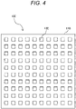
- Fig. 4 is a view illustrating an example of arrangement of a light detection unit according to an embodiment of the present disclosure.
- This figure is a view illustrating an example in which the plurality of light detection units 130 is arranged in the recess 110 of the base material unit 200.
- the plurality of light detection units 130 can be arranged in a two-dimensional lattice pattern. Note that, in the figure, the light detection units 130 are arranged in ten rows and ten columns, but the number of the light detection units 130 is not limited.
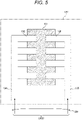
- Fig. 5 is a view illustrating a configuration example of a light detection unit according to an embodiment of the present disclosure.
- This figure is a view illustrating a configuration example of the light detection unit 130.
- the light detection unit 130 in the figure includes a photoconductor 131 and electrodes 132 and 133.
- Electrical conductivity of the photoconductor 131 changes in accordance with emitted light.
- a photoconductor including graphene can be used as the photoconductor 131.
- the photoconductor 131 in the figure is configured by a thin film of graphene.
- the electrodes 132 and 133 are electrodes connected to the photoconductor 131. These electrodes 132 and 133 are arranged on a surface of the photoconductor 131 and are separately arranged at positions facing each other.
- the electrodes 132 and 133 can include, for example, gold (Au).
- a plurality of electrodes 132 and a plurality of electrodes 133 are arranged and connected to wiring lines 134 and 135, respectively.
- the wiring lines 134 and 135 are individually connected to the signal line 301.
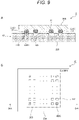
- Fig. 6 is a view illustrating an example of light emission of a stress light emitting body according to an embodiment of the present disclosure.
- This figure is a view illustrating a state of light emission of the stress light emitting body 120 when stress is applied to a connection part between the terminal 21 and the land 100.
- a solid-line rectangle represents the land 100.
- a solid-line circle represents the stress light emitting body 120, and hatching inside the circle represents intensity of light emission of the stress light emitting body 120. As a density of the hatching is higher, higher intensity of the light emission is represented.
- a chain-line circle represents the terminal 21 joined to the land 100.
- a of the figure is a view illustrating a state of the land 100 immediately after the electronic component 20A is mounted. Since the terminal 21 is spherical, stress is strongly applied to a central portion of a region where the terminal 21 is joined. Therefore, the stress light emitting body 120 arranged in the central portion of the region where the terminal 21 is joined strongly emits light.
- B of the figure is a view illustrating an example of a case where distortion occurs in the substrate 10 and the electronic component 20A, and stress is applied to a joint part between the terminal 21 and the land 100.
- a hollow arrow in B in the figure indicates a direction of the stress.
- the stress is applied in a right direction of the page, which increases the number of stress light emitting bodies 120 that strongly emit light.
- positions of the stress light emitting bodies 120 that emit light shift in the right direction.
- Fig. 7 is a diagram illustrating a configuration example of a stress detection unit according to the first embodiment of the present disclosure.
- the stress detection unit 300 in the figure includes a power supply unit 310, a comparison unit 320, and a damage detection unit 330.
- the power supply unit 310 supplies power to the light detection unit 130.
- This power supply unit 310 can be configured by a constant voltage power supply.
- the power supply unit 310 applies a power supply voltage to any one of the wiring lines 134 and 135 described in Fig. 5 , for example, the wiring line 135 via one of two signal lines 301.
- the wiring line 134 is connected to the comparison unit 320 described later, via another one of the signal lines 301.
- the power supply unit 310 is commonly connected to the signal lines 301 connected to the individual light detection units 130.
- the comparison unit 320 detects stress by comparing a light detection signal from the light detection unit 130 with a predetermined threshold value. This comparison unit 320 can detect stress in a case where the light detection signal is larger than a predetermined threshold value. Note that, in a case where the plurality of light detection units 130 is arranged, the comparison unit 320 individually compares each of the light detection signals from the plurality of light detection units 130 with the threshold value.
- the damage detection unit 330 detects damage of the joint part between the terminal 21 and the land 100 on the basis of stress detected by the comparison unit 320.
- the damage detection unit 330 can detect damage when the comparison unit 320 detects stress.
- the damage detection unit 330 can also detect damage on the basis of the number of light detection units 130 corresponding to the detected stress.
- the damage detection unit 330 can also detect damage on the basis of an area occupied by the light detection unit 130 corresponding to the detected stress.
- the damage detection unit 330 outputs a detection signal to outside when damage is detected. Furthermore, the damage detection unit 330 can also directly output stress detected by a comparison unit 340 ( Fig. 8 ). In this case, a distribution of the stress in the land 100 can be displayed as an image. By arranging the stress detection unit 300, it is possible to confirm damage of the substrate 10 incorporated the electronic device or the semiconductor package, from outside. Furthermore, the damage of the substrate 10 can be detected even during an operation of the electronic device or the like.
- the substrate 10 by detecting light emitted from the stress light emitting body 120 arranged in the land 100 by using the light detection unit 130 arranged at the bottom part of the land 100, stress in the joint part between the terminal 21 and the land 100 can be detected. As a result, it is possible to detect damage of the joint part between the terminal 21 and the land 100.
- the stress is detected by comparing the light detection signal with the predetermined threshold value, in the stress detection unit 300.
- a substrate 10 according to a second embodiment of the present disclosure is different from the above-described first embodiment in that stress is detected by detecting a change in a light detection signal.
- Fig. 8 is a diagram illustrating a configuration example of a stress detection unit according to the second embodiment of the present disclosure.
- This figure is a diagram illustrating a configuration example of a stress detection unit 300 similarly to Fig. 7 .
- a comparison unit 340 is arranged instead of the comparison unit 320, and a holding unit 350 is further provided.
- the comparison unit 340 detects a change in stress when a light detection signal changes.
- this comparison unit 340 causes the holding unit 350 to hold a light detection signal from a light detection unit 130 as an initial value. Thereafter, the comparison unit 340 can detect a change in stress on the basis of a light detection signal outputted by the light detection unit 130 and the light detection signal held by the holding unit 350. Specifically, generation of new stress can be detected by detecting a difference between the light detection signal outputted from the light detection unit 130 and the light detection signal held by the holding unit 350. The newly detected stress can be compared with a predetermined threshold value.
- the comparison unit 340 can also compare the light detection signal outputted from the light detection unit 130 with the light detection signal held in the holding unit 350, to detect a change (decrease) in stress in a case where the light detection signal outputted by the light detection unit 130 decreases.
- a change in stress in a case where the light detection signal outputted by the light detection unit 130 decreases.
- damage such as detachment of the terminal 21 from the land 100 can be detected by detecting a decrease in the light detection signal outputted by the light detection unit 130.
- the detection of damage can be performed by the damage detection unit 330.
- the holding unit 350 is configured to hold a light detection signal for each light detection unit 130.
- This holding unit 350 includes a memory or the like, and holds a light detection signal and outputs the held light detection signal to the comparison unit 340 on the basis of control of the comparison unit 340.
- a configuration of the substrate 10 other than this is similar to the configuration of the substrate 10 described in the first embodiment of the present disclosure, and thus a description thereof will be omitted.
- the substrate 10 according to the second embodiment of the present disclosure can detect a change in stress by comparing a light detection signal held by the holding unit 350 with a newly detected light detection signal. As a result, it is possible to detect progress of damage of the joint part between the terminal 21 and the land 100.
- a semiconductor package 2 according to a third embodiment of the present disclosure will be described in detail with reference to Figs. 9 and 10 .
- the same parts as those in the first and second embodiments are denoted by the same reference numerals, and a redundant description is avoided.
- Fig. 9 illustrates the semiconductor package 2 according to the present embodiment.
- An electronic component 20B provided in the semiconductor package 2 of the present embodiment uses a package structure of a ball grid allay (BGA) type, and is connected to a land 100 on a substrate 10 side with a large number of terminals 21. Note that the electronic component 20B is an example of an element described in the claims.
- BGA ball grid allay
- a plurality of electronic components can be mounted on the substrate 10.
- the substrate 10 may be a circuit substrate on which a surface-mounted semiconductor component, chip resistor, and the like are mounted, and a substrate of a semiconductor package on which a semiconductor chip is bare chip-mounted.
- corner lands 100C other lands 100 excluding lands 100 (hereinafter, referred to as "corner lands 100C") at corners, for example, four corner portions, are electrically connected to each other by wiring lines not illustrated.
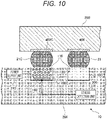
- stress light emitting bodies 150 are provided only in the corner lands 100C at four corner portions among the large number of lands 100 provided in a lattice pattern on the substrate 10. This is because it has been found that, in a case where damage such as a crack occurs in the terminals 21, the crack or the like is likely to occur first in a terminal 21 (hereinafter referred to as a "corner terminal 21C") connected to the corner land 100C. Furthermore, light detection units 160 are also installed inside the corner lands 100C at the four corners.
- the corner terminal 21C has only a function of simply electrically energizing a power supply unit 310 with a constant voltage power supply having a configuration similar to that of the first embodiment, instead of connecting between the electronic component 20B side and the substrate 10 side. Therefore, this corner terminal 21C repeats energization in synchronization with ON/OFF of the power supply accompanying use of an electronic device provided with the semiconductor package 2.
- this corner terminal 21C is for predicting breakage of terminals 21 other than the corner terminal 21C. That is, the corner terminal 21C is not configured to function as a part of a signal line for exchange of data between the electronic component 20B and the substrate 10 side. Therefore, the corner terminal 21C is connected only to an electrode 400C inside the electronic component 20B, and is not connected by a wiring line to other functional units including other electrodes 400 inside the electronic component 20B.
- a plurality of recesses 110 is provided in a lattice pattern on an upper surface of a base material unit 200, and the lands 100 and 100C are installed in these recesses 110.
- the lands 100 and 100C are arranged according to the terminals 21 and 21C of the electronic component 20B to be mounted.
- the corner land 100C is a conductor to which the corner terminal 21 is joined, and is installed in the recess 110 similarly to other lands 100.
- a conductive transparent resin body similar to that of the first embodiment is used, and the stress light emitting bodies 150 are mixed in a dispersed state.
- electrical connection between with the corner terminal 21C can be made by performing thermocompression on the terminal 21C such as a solder ball.
- the lands 100 other than the corner lands 100C do not particularly need to include a conductive transparent resin.
- Other lands 100 can be formed by a metal having good conductivity such as gold (Au) or copper (Cu).
- the land 100 and the electrode of the electronic component 20B can be electrically connected by the terminal 21 such as a solder ball.
- the stress light emitting body 150 by using a mechanoluminescence particle that emits light when a force is applied to an object or the like and the force is converted into light energy, a light emission phenomenon of the mechanoluminescence particle can be used, which similarly applies to the first embodiment.
- a sheet-shaped one hereinafter referred to as a "stress light emitting sheet" in which mechanoluminescence particles are mixed in a thin transparent conductive resin body can be used. Since the stress light emitting sheet is thinner than the stress light emitting body 150 of the bulk-shaped corner land 100C having a certain thickness, stress easily propagates directly. Furthermore, an optical distance until an internal light emission ray propagating to outside is also short as the stress light emitting sheet is thin, and an attenuation amount is small accordingly, so that the stress light emitting sheet can emit light with high intensity.
- the stress light emitting body 150 is not necessarily installed in the corner land 100C.
- the stress light emitting body 150 may be provided between an upper side of the corner terminal 21C and the electrode 400C side of the electronic component 20B.
- a stress light emitting sheet in which a stress light emitting body is mixed in a conductive transparent resin body can be used.
- the light detection unit 160 can be configured by an appropriate photoelectric conversion means or the like that outputs an electric signal in accordance with a received light amount or received light intensity when receiving light emitted from the stress light emitting body 150. That is, as the light detection unit 160, an optical sensor that generates a predetermined electromotive current (a photocurrent or an electromotive force) when receiving light having a wavelength emitted from the stress light emitting body 150, for example, a photodiode, a phototransistor, or the like can be used, which similarly applies to the first embodiment.
- the light detection unit of the present disclosure only needs to be capable of detecting light having a wavelength emitted from the stress light emitting body.
- the light detection unit 160 of the present embodiment is embedded in a bottom part of the recess 110 in which the corner land 100C of the base material unit 200, which is the substrate 10, is installed.
- this light detection unit 160 a light detection unit having a configuration similar to that of the light detection unit 130 of the first embodiment illustrated in Fig. 5 can be used.
- the stress detection unit 300 as illustrated in Fig. 7 or 8 is connected for output signal processing of this light detection unit 160.
- the light detection unit 160 may not be installed as long as a light emission phenomenon of the stress light emitting body 150 in the corner land 100C can be directly visually recognized from outside the substrate 10.
- the corner terminal 21C is damaged to have a crack first before other terminals 21, due to energization to the electronic component 20B many times.
- the stress concentrated on the damaged corner terminal 21C propagates to the stress light emitting body 150 in the corner land 100C to cause a light emission phenomenon.
- the light detection unit 160 that has received the light outputs a light detection signal.
- the light detection signal generates and outputs an electric signal corresponding to intensity of emitted light. As a result, it is possible to detect that the corner terminal 21C is damaged.
- damage of the substrate 10 incorporated in the electronic device or the semiconductor package can be confirmed from outside. Furthermore, even during an operation of the electronic component 20B or the like, damage of the substrate 10 can be detected.
- the light detection unit 160 for detection of damage is installed only in the corner land 100C on the basis of findings from the experimental example described later. Therefore, the damage of the terminal 21 can be detected only with a minimum number of stress light emitting bodies 150 and light detection units 160 installed, and the cost can be reduced.
- the light detection unit is not required. Therefore, there is an effect that the cost can be further reduced.
- strong light emission can be achieved by using the stress light emitting sheet as the stress light emitting body 150, visual recognition from outside is easier and more reliable, which is convenient.
- the corner terminal 21C does not have any function as a signal line for exchange of data.
- the corner terminal 21C is not connected to other electrodes 400 or others inside the electronic component 20B by a wiring line. Therefore, even if the corner terminal 21C has breakage such as a crack, the electronic component 20B can be continuously used as it is.
- Fig. 11 is a schematic view illustrating a state where a large number of terminals 21 (hereinafter, in this example, referred to as solder balls 21) such as solder balls provided in a semiconductor package 20 having a BGA structure similar to that used in the third embodiment are arranged in a lattice pattern on a substrate 10.
- solder balls 21 such as solder balls provided in a semiconductor package 20 having a BGA structure similar to that used in the third embodiment are arranged in a lattice pattern on a substrate 10.
- solder ball 21 among the large number of solder balls 21 arranged and connected to individual lands (not illustrated) is particularly likely to have a crack when a current is applied to and cut off from an electronic component 20 many times.
- a metal alloy or the like including a plurality of dissimilar metal atoms such as solder for example, along with a thermal action received due to energization of the electronic component, an atomic lattice in the metal is likely to generate thermal vibration and diffusion, and a lattice defect is likely to be generated in a part of the atomic lattices.
- a diffusion rate of each metal atom varies depending on a type. Therefore, a microscopic atomic defect is likely to grow largely due to a deviation in diffusion rate at a joint site or the like between different kinds of metal atoms. When such a thermal history is repeatedly received, the atomic defect further progresses.
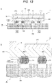
- FIG. 12 A graph created on the basis of data obtained by the experiment at this time is illustrated in Fig. 12 .
- the graph in the figure is a log-log graph in which a horizontal axis indicates a cumulative total number of energization (the number of cycles) when energization to the electronic component 20 is actually performed, and a vertical axis indicates an accumulated percentage (%) of a failure rate due to an occurrence of a crack and the like.
- Fig. 11 schematically illustrates a specific occurrence situation of a failure portion obtained for each of the solder balls 21 arranged in a lattice pattern on the substrate 10.
- the solder ball 21 at a location with a larger number of dots indicates a higher resistance value (larger damage). That is, it is indicated that the number of occurrences (failure rate) of damage such as a crack is large due to concentrated application of the stress.
- a sample photograph is also shown in which a crack generation site is captured as a specific cleavage.
- Each of the sample photographs shows a captured image of the solder balls 21 at corners of a lowermost right portion (No. 1) and an uppermost right portion (No. 14) among the large number of solder balls 21 arranged in a lattice pattern.
- the solder ball 21 is in a state of being collapsed upward and downward.
- This solder ball 21 has a lower part connected to a land and an upper part connected to an electrode of an electronic component.
- the solder balls 21C at the corner portions of the four corners have a large number of occurrences (failure rate) of damage such as a crack in particular, among the solder balls 21 connected to the individual lands. This may be because stress tends to concentrate on the four corner portions of the semiconductor package 20.
- the configuration of the third embodiment has been conceived. That is, in the embodiment of the present disclosure, the stress light emitting body 150 is particularly installed only in the corner land 100C corresponding to the corner terminal 21C among the terminals 21 and the lands 100 arranged in a large number in a lattice pattern.
- the light detection unit 160 Furthermore, by monitoring light emission from the stress light emitting body 150 attached inside the corner land 100C by using the light detection unit 160, damage to a terminal of an electronic component can be detected early and effectively, and a failure due to deterioration over time of the electronic component can be confirmed in advance.
- a semiconductor package 3 according to a fourth embodiment of the present disclosure will be described in detail with reference to Fig. 13 .
- the same parts as those in the first to third embodiments are denoted by the same reference numerals, and a redundant description is avoided.
- the semiconductor package 3 of the present embodiment is similar to that of the previous embodiment in that an electronic component 20C having a BGA structure is used.
- an upper surface of an interposer 20D on which the electronic component 20C is mounted is sealed with a side plate 30 and a ceiling plate 40.
- the semiconductor package 3 of the present embodiment is different from the semiconductor packages 1 and 2 according to the first to third embodiments in that a conductive transparent resin body 150 (hereinafter, referred to as a stress light emitting block 170) in which stress light emitting bodies 120 (see B of the figure) are dispersed and mixed is particularly provided to corner terminals 21C at four corners among terminals 21 for connection with a large number of lands 100 provided on a substrate 10, and a light detection unit is not installed.
- a conductive transparent resin body 150 hereinafter, referred to as a stress light emitting block 170
- stress light emitting bodies 120 see B of the figure
- the stress light emitting block 170 of the present embodiment is provided on an outer surface of the corner terminal 21C so as to be observable not from inside a corner land 100C but from outside. That is, it is not necessary to provide a conductive transparent resin body or a stress light emitting body inside the corner land 100C.
- a stress light emitting body provided at the corner terminal 21C may have a configuration in which the stress light emitting body is dispersed and mixed in a transparent resin body having conductivity and formed in a sheet shape (this is referred to as a stress light emitting sheet 170S) instead of being provided as a block form as described above.
- the stress light emitting block 170 and the stress light emitting sheet 170S preferably emit light having a wavelength in a visible light region.
- the stress light emitting block 170 is attached only to the corner terminal 21C, which is susceptible to damage such as a crack, that is, a terminal at the corner facing outside, on the basis of the findings in the above-described experimental example. Therefore, the light emission phenomenon can be visually recognized directly from outside with respect to the corner terminal 21C, which is highly likely to be broken first among the terminals. Furthermore, the terminal that should be visually recognized is located on an outermost portion, which is particularly easily found first, in the terminals arranged in a lattice pattern. Accordingly, breakage of the corner terminal 21C can be easily and reliably confirmed from outside.
- the stress light emitting body is of a type that emits light having a specific wavelength outside visible light (for example, a near infrared ray, a near ultraviolet ray, and the like), it is only required to prepare a light detection unit configured to detect light in the wavelength region in the semiconductor package 3 or in the vicinity thereof.
- a light detection unit configured to detect light in the wavelength region in the semiconductor package 3 or in the vicinity thereof.
- the stress light emitting block 170 or the stress light emitting sheet 170S is only required to be directly attached to an outer surface of the corner terminal 21C instead of inside the lands 100 and 100C. Therefore, installation work is simple, and the cost can be greatly reduced. In particular, in a case where a light emission ray from the stress light emitting block 170 or the stress light emitting sheet 170S is visible light, the light detection unit is not required, so that the cost can be further reduced.
- the stress light emitting block 170 or the stress light emitting sheet 170S when it is necessary to confirm damage such as a crack of the terminal 21 after manufacturing the electronic device including the semiconductor package 3, it is only required to attach the stress light emitting block 170 or the stress light emitting sheet 170S to the terminal 21. Therefore, even if the stress light emitting block 170 or the stress light emitting sheet 170S is installed later, an occurrence of damage such as a crack can be detected.
- semiconductor packages 4A and 4B according to a modification of the fourth embodiment of the present disclosure will be described in detail with reference to Fig. 14 .
- the same parts as those of the first to fourth embodiments are denoted by the same reference numerals, and a redundant description is avoided.
- a side wall plate 30 including an appropriate plastic resin material is fixed, with an adhesive, to an upper surface of an interposer 20D on which an electronic component 20C is mounted.
- a ceiling plate 40 including a transparent sealing material such as a glass body is fixed with an adhesive.
- an adhesive is likely to cause damage such as cleavages, crazes, and cracks (solvent cracks) due to a temperature and environmental change, and the like.
- damage such as cleavages, crazes, and cracks (solvent cracks) due to a temperature and environmental change, and the like.
- the additive enters from an adhesion interface into an object that is to be bonded, and a defect occurs at the interface or the like to cause breakage, a cleavage, or the like. Therefore, it is preferable not to include a component that is likely to cause a defect as a component of the adhesive.
- a stress light emitting sheet 170S' similar to that described in the fourth embodiment is attached outside the adhesive between the interposer 20D and the side plate 30.
- a similar stress light emitting sheet 170S' is attached outside the adhesive between the side wall plate 30 and the ceiling plate 40.
- the stress light emitting sheet 170S' of the first and second modifications is obtained by dispersing and mixing a stress light emitting body in a transparent resin body formed in a sheet shape, for example, and does not need to be conductive as the stress light emitting sheet 170S described in the fourth embodiment.
- the light detection unit is not provided similarly to the case of the fourth embodiment, but a light detector may be provided around the semiconductor packages 4A and 4B to detect light emitted from the stress light emitting sheet.
- a configuration may be adopted in which the entire electronic component 20C is molded and sealed with a plastic resin instead of the side wall plate 30 and the ceiling plate 40 as in the configuration of the present embodiment. In this case, the stress light emitting sheet can be attached to a boundary between the plastic resin and the interposer.
- the stress light emitting sheet 170S' described above in a case where damage such as a cleavage and a crack occurs at an interface or the like in accordance with a change in temperature, environment, or the like of each adhesive, strong stress is generated in the stress light emitting sheet 170S' attached to the adhesive to cause emission of visible light. Therefore, an observer can observe and confirm the light beam with the naked eye from outside.
- the cost can be reduced accordingly. Furthermore, in any of the modifications, since the stress light emitting sheet 170S' is not embedded in the lands 100 and 100C, manufacturing is easy and the cost can be reduced accordingly. Moreover, similarly to the fourth embodiment, the stress light emitting sheet 170S' can be attached later. Moreover, installation work of the stress light emitting sheet 170S' can be easily and simply performed.
- a semiconductor package 2 according to a fifth embodiment of the present disclosure will be described in detail with reference to Fig. 15 .
- the same parts as those in the first to fourth embodiments are denoted by the same reference numerals, and a redundant description is avoided.
- the semiconductor package 5 of the present embodiment is different from the semiconductor package 3 of the fourth embodiment in that an image capturing means 180 is installed as a means for detection of light emission from a stress light emitting sheet 170S, instead of confirmation with the naked eye.
- the image capturing means 180 a video camera, a digital camera, or the like using an individual imaging element such as a charge coupled device image sensor (CCD image sensor) or a complimentry metal oxcide imege sensor (CMOS image sensor) can be used. Furthermore, an imaging signal outputted from the image capturing means 180 may be extracted to outside via a signal line and recorded by an image recording means or the like. Furthermore, this light emission detection means is not necessarily limited to the image capturing means 180 and the image recording means. Various light emission detection means such as a light detector can be applied, this light emission detection means may be installed around the semiconductor package.
- CCD image sensor charge coupled device image sensor
- CMOS image sensor complimentry metal oxcide imege sensor
- the stress light emitting sheet 170S is attached to a corner terminal 21C, which is particularly susceptible to damage such as a crack, that is, an outermost terminal facing the outside. Therefore, for example, light emission emitted from the stress light emitting sheet 170S can be captured by the image capturing means 180 such as a video camera. Therefore, in a case of a configuration in which the captured image is recorded, even if the observer is not always observing the captured image, an abnormality such as damage of a terminal 21 can be easily confirmed at any time thereafter.
- the application range of the present disclosure is not particularly limited to the substrate or the semiconductor package of the present disclosure.
- the stress light emitting body, the light detection unit, or the like of the present disclosure may be installed to detect the damage.
- the stress light emitting sheet or the like of the present disclosure may be provided at a site that is likely to be damaged by multiple sterilization operations by an autoclave, and the presence or absence of damage may be detected in advance prior to sterilization and disinfection work.
- the stress light emitting sheet, the light detection unit, or the like of the present disclosure may be installed in advance on a component that is likely to be damaged.
- the processing procedure described in the embodiment described above may be regarded as a method having a series of these procedures, and may be regarded as a program for causing a computer to execute the series of procedures, or a recording medium storing the program.
- this recording medium for example, a compact disc (CD), a digital versatile disc (DVD), a memory card, and the like can be used.
Landscapes
- Engineering & Computer Science (AREA)
- Physics & Mathematics (AREA)
- General Physics & Mathematics (AREA)
- Microelectronics & Electronic Packaging (AREA)
- Computer Hardware Design (AREA)
- General Engineering & Computer Science (AREA)
- Electric Connection Of Electric Components To Printed Circuits (AREA)
- Led Device Packages (AREA)
- Testing Of Short-Circuits, Discontinuities, Leakage, Or Incorrect Line Connections (AREA)
- Tests Of Electronic Circuits (AREA)
Abstract
Description
- The present disclosure relates to a substrate and a semiconductor package. Specifically, the present disclosure relates to a substrate on which an element such as an electronic component is mounted, and a semiconductor package.
- Conventionally, a device that detects damage to a substrate on which an electronic component is mounted has been proposed. For example, a device that detects disconnection of a wiring line arranged in a substrate by using an organic light emitting element has been proposed (see, for example, Patent Document 1).
- This organic light emitting element is an element in which a light emitting layer is sandwiched between an anode and a cathode, and a voltage is applied to the light emitting layer via the anode and the cathode to cause light emission. Furthermore, in the organic light emitting element, a common anode and a plurality of cathodes respectively corresponding to a plurality of wiring lines to be inspected are arranged. At a time of detecting disconnection of the wiring line of the substrate, the cathode is brought into contact with one end of the wiring line to be inspected, and a voltage is applied between another end of the wiring line and the anode to cause the organic light emitting element to emit light. Since the organic light emitting element does not emit light in the wiring line in which the disconnection has occurred, the disconnection of the wiring line can be detected.
- Furthermore, there has been proposed a module capable of detecting breakage of a bonding material connecting an active element and a circuit pattern at a joint part and predicting a failure of a circuit substrate including the joint part of the active element (see Patent Document 2). In this module, a detection circuit is separately provided on the substrate in the vicinity of an electronic component having a large amount of current and a large amount of heat generation. Furthermore, this detection circuit includes a first conductor including different metal or different alloy and a second conductor detector joined to the first conductor. Note that the electronic component includes a plurality of electrodes, and the electrodes are connected to the circuit pattern of the substrate via gold bumps.
- In such a module, when the detector included in the detection circuit is heated by heat generated by the electronic component, breakage occurs at a joint part between the first conductor and the second conductor constituting the detector, and disconnection occurs. As a result, conduction cannot be achieved before failure in the circuit substrate itself, so that failure of the circuit substrate can be predicted.
-
- Patent Document 1:
Japanese Patent Application Laid-Open No. H09-015288 - Patent Document 2:
Japanese Patent Application Laid-open No. 2011-209199 - In the related art described in
Patent Document 1 described above, there is a problem that breakage of a substrate on which an electronic component is mounted cannot be detected. The electronic component is mounted, for example, by joining a terminal of the electronic component to a land arranged in the substrate. This joining is performed by soldering, for example. Furthermore, the substrate on which the electronic component is mounted is used by being mounted on an electronic device. During use of the electronic device, a joint part between the terminal of the electronic component and the land of the substrate may be damaged. For example, due to a change in temperature during use, the substrate and the electronic component repeat expansion and contraction. In a case where thermal expansion coefficients of the substrate and the electronic component are different from each other, a difference in displacement between expansion and contraction occurs, and stress is generated in a joint portion. When this stress increases, damage such as breakage of the joint part occurs. In the related art described inPatent Document 1 described above, there is a problem that it is not possible to detect such damage in the joint part of the terminal of the electronic component. - Whereas, in the related art described in
Patent Document 2, the detector provided in the detection circuit detects an occurrence of a failure of a joint part or the like connecting the electronic component and the circuit pattern due to heat generation of the electronic component. However, in order to sense the breakage, it is necessary to specially install separately the detection circuit on the substrate. - The present disclosure has been made in view of the above-described problems, and an object is to enable to detect damage of a joint part between with a terminal of a mounted electronic component and damage of a semiconductor package, without installing a detection circuit on a substrate.
- The present disclosure has been made to solve the above-described problems, and a first aspect thereof is a substrate including: a base material unit; a land arranged with a stress light emitting body that emits light in accordance with stress, including a transparent member, arranged in the above-described base material unit, and joined with a terminal of an element; and a light detection unit arranged between the above-described base material unit and the above-described land and configured to detect light from the stress light emitting body.
- Furthermore, in this first aspect, the above-described stress light emitting body may be particularly arranged only in a land at a corner among a plurality of lands to which a plurality of terminals of the above-described element is joined.
- Furthermore, in this first aspect, a terminal at a corner joined to the land at the corner described above may have a wiring structure not having a function as a signal line through which an electric signal passes between inside and outside of the element.
- Furthermore, in this first aspect, the above-described light detection unit may output an electric signal according to light from the above-described stress light emitting body as a result of the above-described detection.
- Furthermore, in this first aspect, a stress detection unit configured to detect stress in the above-described land on the basis of a detection result in the above-described light detection unit may be further included.
- Furthermore, in this first aspect, the above-described stress detection unit may detect the above-described stress by comparing a detection result in the above-described light detection unit with a predetermined threshold value.
- Furthermore, in this first aspect, the above-described stress detection unit may detect the above-described stress when a detection result of the above-described light detection unit changes.
- Furthermore, in this first aspect, a holding unit configured to hold a detection result of the above-described light detection unit may be further included, and the above-described stress detection unit may detect a change in a detection result of the above-described light detection unit by comparing a detection result of the above-described light detection unit with a detection result held by the holding unit.
- Furthermore, in this first aspect, a plurality of the above-described light detection units may be arranged between the above-described base material unit and the above-described land, and the above-described stress detection unit may detect the above-described stress on the basis of detection results of the above-described plurality of light detection units.
- Furthermore, in this first aspect, a damage detection unit configured to detect damage of a joint part between the above-described terminal and the above-described land on the basis of the above-described detected stress may be further included.
- Furthermore, in this first aspect, the above-described land may be bonded to a terminal of the element to be joined to the terminal.
- Furthermore, in this first aspect, the above-described land may be arranged in a recess formed in the above-described base material unit.
- According to the first aspect of the present disclosure, an effect is provided that light emission of the stress light emitting body arranged in the land is detected. Detection of stress in the joint part between the terminal and the land is assumed.
- A second aspect of the present disclosure is a semiconductor package including: a substrate on which a semiconductor provided with a large number of terminals is mounted; and a stress light emitting body provided on a terminal side and/or a package side and configured to emit light when the terminal of the semiconductor and/or the package of the semiconductor described above is damaged, in which light emission of the above-described stress light emitting body is detected from outside.
- Furthermore, in the second aspect of the present disclosure, the stress light emitting body may be a sheet-shaped stress light emitting body provided on an adhesive that bonds between the substrate side and a resin body and/or a glass body to be an external structure of the package.
- Furthermore, in the second aspect of the present disclosure, a light beam emitted by light emission of the above-described stress light emitting body may include a wavelength other than a wavelength in a visible light band, such as a wavelength of an ultraviolet ray or a near infrared ray.
- Furthermore, in the second aspect of the present disclosure, the above-described stress light emitting body may be provided only on a terminal at a corner portion among terminals of the semiconductor.
- Furthermore, in the second aspect of the present disclosure, a light detector may be installed around the above-described package.
- Furthermore, in the second aspect of the present disclosure, in the above-described stress light emitting body, any material may be usable from among: strontium aluminate (SrAl2O4:Eu) doped with europium and structurally controlled; zinc sulfide (ZnS:Mn) or barium calcium titanate ((Ba, Ca) TiO3:Pr) doped with a transition metal or a rare earth; and calcium yttrium aluminate (CaYAl3O7:Ce)
- Furthermore, according to the second aspect of the present disclosure, damage of the terminal of the semiconductor and/or the package of the semiconductor can be directly confirmed from outside by directly viewing light emission of the stress body from outside.
-
-
Fig. 1 is a schematic view illustrating a configuration example of a substrate according to a first embodiment of the present disclosure. -
Fig. 2 is a cross-sectional view illustrating a configuration example of the substrate according to the first embodiment of the present disclosure. -
Fig. 3 is an enlarged cross-sectional view illustrating a configuration example of a land portion of the substrate according to the first embodiment of the present disclosure. -
Fig. 4 is a schematic view illustrating an example of arrangement of a light detection unit according to the first embodiment of the present disclosure. -
Fig. 5 is a schematic view illustrating a configuration example of the light detection unit according to the first embodiment of the present disclosure. -
Fig. 6 is a schematic view illustrating an example of light emission of a stress light emitting body according to the first embodiment of the present disclosure, in which A illustrates an example immediately after mounting, and B illustrates an example of a change in light emission when stress is applied. -
Fig. 7 is a schematic diagram illustrating a configuration example of a stress detection unit according to the first embodiment of the present disclosure. -
Fig. 8 is a schematic diagram illustrating a configuration example of a stress detection unit (a modification of the stress detection unit according to the first embodiment) according to a second embodiment of the present disclosure. -
Fig. 9(A) is a schematic view illustrating a configuration example of a semiconductor package according to a third embodiment of the present disclosure, andFig. 9(B) is a schematic plan view ofFig. 9(A) . -
Fig. 10 is an enlarged schematic cross-sectional view illustrating a configuration example of a land and the like in a corner portion among lands of a substrate according to the third embodiment of the present disclosure. -
Fig. 11 is an explanatory view illustrating terminal arrangement of a semiconductor having a BGA structure used in an experimental example of the present disclosure used to obtain a basic configuration of the third and subsequent embodiments of the present disclosure. -
Fig. 12 is a graph showing a relationship between a failure rate of each terminal and the number of times of energization to each terminal performed in the experimental example of the present disclosure in each terminal of the semiconductor illustrated inFig. 11 , and an explanatory view illustrating experimental data obtained from the experimental example of the present disclosure for obtaining a failure frequency of each terminal arranged in a large number. -
Fig. 13(A) is a schematic view illustrating a configuration example of a semiconductor package according to a fourth embodiment of the present disclosure, andFig. 13(B) is an enlarged cross-sectional view of a corner portion ofFig. 13(A) . -
Fig. 14(A) is a schematic view illustrating a first modification of the semiconductor package according to the fourth embodiment of the present disclosure, andFig. 14(B) is a schematic view illustrating a second modification of the semiconductor package according to the fourth embodiment of the present disclosure. -
Fig. 15 is a schematic view illustrating a configuration example of a light detection unit according to a fifth embodiment of the present disclosure. - Next, embodiments for carrying out the present disclosure (hereinafter, referred to as embodiments) will be described with reference to the drawings. In the following drawings, the same or similar parts are denoted by the same or similar reference numerals. Furthermore, embodiments will be described in the following order.
- 1. First embodiment
- 2. Second embodiment
- 3. Third Embodiment (including experimental example)
- 4. Fourth embodiment
- 5. Modification of fourth embodiment
- 6. Fifth embodiment
-
Fig. 1 is a view illustrating a configuration example of asubstrate 10 of a semiconductor package according to an embodiment of the present disclosure. Thesubstrate 10 in the figure includes abase material unit 200 and aland 100. - The
base material unit 200 is a plate-shaped base material constituting thesubstrate 10. Theland 100 is arranged on a surface of thisbase material unit 200. Theland 100 is a conductor to which a terminal of an electronic component or the like is joined. Theland 100 in the figure represents an example of a land formed in a rectangular shape. Theland 100 is arranged according to the terminal of the electronic component to be mounted. This figure represents an example in which a plurality oflands 100 is arranged in a rectangular shape. Note that a plurality of electronic components can be mounted on thesubstrate 10. Thelands 100 are electrically connected to each other by wiring lines (not illustrated). Note that thesubstrate 10 corresponds to a circuit substrate on which a surface-mounted semiconductor component, chip resistor, and the like are mounted, and a substrate of a semiconductor package on which a semiconductor chip is bare chip-mounted. -
Fig. 2 is a cross-sectional view illustrating a configuration example of thesubstrate 10 of asemiconductor package 1 according to an embodiment of the present disclosure. This figure is a view illustrating a state where anelectronic component 20A is mounted on thesubstrate 10. Theelectronic component 20A includes a terminal 21. The terminal 21 in the figure is an example of being configured by a spherical metal such as a solder ball. Theelectronic component 20A is mounted on thesubstrate 10 by this terminal 21 being joined to theland 100 of thesubstrate 10. Thesubstrate 10 in the figure represents an example of being formed in a shape in which theland 100 is embedded in thebase material unit 200. - Note that, to the
terminal 21 of theelectronic component 20A, a lead terminal for surface mounting including copper (Cu) or the like can also be applied. Furthermore, an electrode of chip resistance can also be applied to the terminal 21. Note that theelectronic component 20A is an example of an element described in the claims. - The
electronic component 20A corresponds to a semiconductor element. This semiconductor element is configured by a member having a relatively small thermal expansion coefficient, such as a semiconductor chip. Whereas, thebase material unit 200 is configured by a member having a relatively large thermal expansion coefficient, such as a resin. Therefore, different strains are individually generated in a case where a temperature changes. For example, in a case where a temperature of thesubstrate 10 and theelectronic component 20A rises, thesubstrate 10 expands more than theelectronic component 20A. For this reason, stress is generated at a connection portion between thesubstrate 10 and theelectronic component 20A. Specifically, stress is applied to a joint part between the terminal 21 and theland 100. In a case where this stress is excessive, the joint part is damaged. Furthermore, when a temperature change that causes such distortion is repeated, damage to the joint part may progress to cause breakage of the joint part. In order to improve reliability of thesubstrate 10 on which theelectronic component 20A is mounted, it is necessary to detect such damage of the joint part at an early stage. -
Fig. 3 is a cross-sectional view illustrating a configuration example of a portion of theland 100 of thesubstrate 10 of thesemiconductor package 1 according to the embodiment of the present disclosure. This figure is an enlarged view of a region where theland 100 is arranged inFig. 2 . Thesubstrate 10 includes thebase material unit 200, theland 100, alight detection unit 130, and astress detection unit 300. - As described above, the
base material unit 200 is a plate-shaped base material constituting thesubstrate 10. Thisbase material unit 200 includes an insulator, and theland 100 and a wiring line are arranged. Thisbase material unit 200 can include, for example, resin or ceramic. Furthermore, thebase material unit 200 can also include a composite material. Specifically, thebase material unit 200 formed by impregnating a glass cloth with an epoxy resin can also be used. - As described above, the
land 100 is a conductor to which a terminal of an electronic component or the like is joined. Theland 100 in the figure can include a conductive resin. In this case, theland 100 and the terminal 21 can be joined by the terminal 21 being bonded with the resin constituting theland 100. As described later, theland 100 needs to transmit light, and a transparent resin is used as the resin constituting theland 100. Furthermore, theland 100 in the figure represents an example of being arranged in arecess 110 formed in thebase material unit 200. Theland 100 can be formed in a rectangular shape having a width of 1 mm, for example. - In the
land 100, a stresslight emitting body 120 is arranged. This stresslight emitting body 120 emits light in accordance with this stress applied the self. For this stress light emitting body, for example, zinc sulfide (ZnS) doped with manganese (Mn) can be used. Furthermore, strontium aluminate (SrAl2O4) doped with europium (Eu) can also be used. Furthermore, barium calcium titanate ((Ba, Ca) TiO3) doped with praseodymium (Pr) can also be used. Furthermore, calcium yttrium aluminate (CaYAl3O7) doped with cerium (Ce) can also be used. As the stresslight emitting body 120, a material in which such a stress light emitting body is aggregated in a particle state can be used. The stresslight emitting body 120 can be configured as, for example, a particle having a diameter of 200 nm. Theland 100 in the figure represents an example of a configuration in which a plurality of stresslight emitting bodies 120 is dispersed in a resin constituting theland 100. - In a case where stress is generated at the joint part between the terminal 21 and the
land 100 due to a change in ambient temperature or the like, the stresslight emitting body 120 emits light. By detecting this light emission, the stress in the joint part can be detected. - The
light detection unit 130 is configured to detect light from the stresslight emitting body 120. As thelight detection unit 130, an optical sensor can be used. Thelight detection unit 130 in the figure is arranged at a bottom part of therecess 110. Furthermore, this figure represents an example in which a plurality oflight detection units 130 is arranged. In this way, thelight detection unit 130 can be arranged between thebase material unit 200 and theland 100. Thelight detection unit 130 detects light and outputs a detection result. Specifically, thelight detection unit 130 generates and outputs an electric signal corresponding to the emitted light. Hereinafter, this signal is referred to as a light detection signal. Thelight detection unit 130 in the figure outputs the light detection signal via asignal line 301. - The
stress detection unit 300 detects stress on the basis of a detection result of thelight detection unit 130. Thestress detection unit 300 in the figure detects stress on the basis of light detection signals outputted from the plurality oflight detection units 130. Thestress detection unit 300 can be configured by a semiconductor element such as a microcomputer, and can be incorporated thebase material unit 200. Details of the configuration of thestress detection unit 300 will be described later. -
Fig. 4 is a view illustrating an example of arrangement of a light detection unit according to an embodiment of the present disclosure. This figure is a view illustrating an example in which the plurality oflight detection units 130 is arranged in therecess 110 of thebase material unit 200. As illustrated in the figure, the plurality oflight detection units 130 can be arranged in a two-dimensional lattice pattern. Note that, in the figure, thelight detection units 130 are arranged in ten rows and ten columns, but the number of thelight detection units 130 is not limited. -
Fig. 5 is a view illustrating a configuration example of a light detection unit according to an embodiment of the present disclosure. This figure is a view illustrating a configuration example of thelight detection unit 130. Thelight detection unit 130 in the figure includes aphotoconductor 131 andelectrodes - Electrical conductivity of the photoconductor 131 changes in accordance with emitted light. As the
photoconductor 131, for example, a photoconductor including graphene can be used. Thephotoconductor 131 in the figure is configured by a thin film of graphene. - The
electrodes photoconductor 131. Theseelectrodes photoconductor 131 and are separately arranged at positions facing each other. Theelectrodes electrodes 132 and a plurality ofelectrodes 133 are arranged and connected towiring lines signal line 301. - When light is emitted on the
light detection unit 130 in the figure, electrical conductivity of thephotoconductor 131 between theelectrodes electrodes signal line 301, a current according to the change in electrical conductivity can be detected. Specifically, when light is emitted on thelight detection unit 130 in the figure, the electrical conductivity of thephotoconductor 131 increases, and the current flowing between theelectrodes -
Fig. 6 is a view illustrating an example of light emission of a stress light emitting body according to an embodiment of the present disclosure. This figure is a view illustrating a state of light emission of the stresslight emitting body 120 when stress is applied to a connection part between the terminal 21 and theland 100. In the figure, a solid-line rectangle represents theland 100. A solid-line circle represents the stresslight emitting body 120, and hatching inside the circle represents intensity of light emission of the stresslight emitting body 120. As a density of the hatching is higher, higher intensity of the light emission is represented. Furthermore, a chain-line circle represents the terminal 21 joined to theland 100. - A of the figure is a view illustrating a state of the
land 100 immediately after theelectronic component 20A is mounted. Since the terminal 21 is spherical, stress is strongly applied to a central portion of a region where the terminal 21 is joined. Therefore, the stresslight emitting body 120 arranged in the central portion of the region where the terminal 21 is joined strongly emits light. - B of the figure is a view illustrating an example of a case where distortion occurs in the
substrate 10 and theelectronic component 20A, and stress is applied to a joint part between the terminal 21 and theland 100. A hollow arrow in B in the figure indicates a direction of the stress. As illustrated in B of the figure, the stress is applied in a right direction of the page, which increases the number of stresslight emitting bodies 120 that strongly emit light. Furthermore, positions of the stresslight emitting bodies 120 that emit light shift in the right direction. By capturing such a change in light emission of the stresslight emitting bodies 120, it is possible to detect a change in the stress in the joint part between the terminal 21 and theland 100. -
Fig. 7 is a diagram illustrating a configuration example of a stress detection unit according to the first embodiment of the present disclosure. Thestress detection unit 300 in the figure includes apower supply unit 310, acomparison unit 320, and adamage detection unit 330. - The
power supply unit 310 supplies power to thelight detection unit 130. Thispower supply unit 310 can be configured by a constant voltage power supply. Thepower supply unit 310 applies a power supply voltage to any one of thewiring lines Fig. 5 , for example, thewiring line 135 via one of twosignal lines 301. In this case, thewiring line 134 is connected to thecomparison unit 320 described later, via another one of the signal lines 301. In a case where the plurality oflight detection units 130 is arranged as described inFig. 3 , thepower supply unit 310 is commonly connected to thesignal lines 301 connected to the individuallight detection units 130. - The
comparison unit 320 detects stress by comparing a light detection signal from thelight detection unit 130 with a predetermined threshold value. Thiscomparison unit 320 can detect stress in a case where the light detection signal is larger than a predetermined threshold value. Note that, in a case where the plurality oflight detection units 130 is arranged, thecomparison unit 320 individually compares each of the light detection signals from the plurality oflight detection units 130 with the threshold value. - The
damage detection unit 330 detects damage of the joint part between the terminal 21 and theland 100 on the basis of stress detected by thecomparison unit 320. Thedamage detection unit 330 can detect damage when thecomparison unit 320 detects stress. Furthermore, when the plurality oflight detection units 130 is arranged, thedamage detection unit 330 can also detect damage on the basis of the number oflight detection units 130 corresponding to the detected stress. Furthermore, thedamage detection unit 330 can also detect damage on the basis of an area occupied by thelight detection unit 130 corresponding to the detected stress. - The
damage detection unit 330 outputs a detection signal to outside when damage is detected. Furthermore, thedamage detection unit 330 can also directly output stress detected by a comparison unit 340 (Fig. 8 ). In this case, a distribution of the stress in theland 100 can be displayed as an image. By arranging thestress detection unit 300, it is possible to confirm damage of thesubstrate 10 incorporated the electronic device or the semiconductor package, from outside. Furthermore, the damage of thesubstrate 10 can be detected even during an operation of the electronic device or the like. - As described above, in the
substrate 10 according to the embodiment of the present disclosure, by detecting light emitted from the stresslight emitting body 120 arranged in theland 100 by using thelight detection unit 130 arranged at the bottom part of theland 100, stress in the joint part between the terminal 21 and theland 100 can be detected. As a result, it is possible to detect damage of the joint part between the terminal 21 and theland 100. - In the
substrate 10 of the above-described first embodiment, the stress is detected by comparing the light detection signal with the predetermined threshold value, in thestress detection unit 300. Whereas, asubstrate 10 according to a second embodiment of the present disclosure is different from the above-described first embodiment in that stress is detected by detecting a change in a light detection signal. -
Fig. 8 is a diagram illustrating a configuration example of a stress detection unit according to the second embodiment of the present disclosure. This figure is a diagram illustrating a configuration example of astress detection unit 300 similarly toFig. 7 . There is a difference from thestress detection unit 300 inFig. 7 that acomparison unit 340 is arranged instead of thecomparison unit 320, and a holdingunit 350 is further provided. - The
comparison unit 340 detects a change in stress when a light detection signal changes. In an initial state, thiscomparison unit 340 causes the holdingunit 350 to hold a light detection signal from alight detection unit 130 as an initial value. Thereafter, thecomparison unit 340 can detect a change in stress on the basis of a light detection signal outputted by thelight detection unit 130 and the light detection signal held by the holdingunit 350. Specifically, generation of new stress can be detected by detecting a difference between the light detection signal outputted from thelight detection unit 130 and the light detection signal held by the holdingunit 350. The newly detected stress can be compared with a predetermined threshold value. - Furthermore, the
comparison unit 340 can also compare the light detection signal outputted from thelight detection unit 130 with the light detection signal held in the holdingunit 350, to detect a change (decrease) in stress in a case where the light detection signal outputted by thelight detection unit 130 decreases. In a case where damage of a joint part between a terminal 21 and aland 100 progresses and the terminal 21 is detached from theland 100 or a surface of theland 100 is peeled off, stress in the region is reduced to substantially 0. Such damage such as detachment of the terminal 21 from theland 100 can be detected by detecting a decrease in the light detection signal outputted by thelight detection unit 130. The detection of damage can be performed by thedamage detection unit 330. - The holding
unit 350 is configured to hold a light detection signal for eachlight detection unit 130. This holdingunit 350 includes a memory or the like, and holds a light detection signal and outputs the held light detection signal to thecomparison unit 340 on the basis of control of thecomparison unit 340. - By including the holding
unit 350 and detecting a change in the light detection signal, it is possible to detect progress of damage of the joint part between the terminal 21 and theland 100. - A configuration of the
substrate 10 other than this is similar to the configuration of thesubstrate 10 described in the first embodiment of the present disclosure, and thus a description thereof will be omitted. - As described above, the
substrate 10 according to the second embodiment of the present disclosure can detect a change in stress by comparing a light detection signal held by the holdingunit 350 with a newly detected light detection signal. As a result, it is possible to detect progress of damage of the joint part between the terminal 21 and theland 100. - Next, a
semiconductor package 2 according to a third embodiment of the present disclosure will be described in detail with reference toFigs. 9 and10 . Note that, in the present embodiment, the same parts as those in the first and second embodiments are denoted by the same reference numerals, and a redundant description is avoided. -
Fig. 9 illustrates thesemiconductor package 2 according to the present embodiment. Anelectronic component 20B provided in thesemiconductor package 2 of the present embodiment uses a package structure of a ball grid allay (BGA) type, and is connected to aland 100 on asubstrate 10 side with a large number ofterminals 21. Note that theelectronic component 20B is an example of an element described in the claims. - Also in the present embodiment, a plurality of electronic components can be mounted on the
substrate 10. Note that thesubstrate 10 may be a circuit substrate on which a surface-mounted semiconductor component, chip resistor, and the like are mounted, and a substrate of a semiconductor package on which a semiconductor chip is bare chip-mounted. Although details will be described later,other lands 100 excluding lands 100 (hereinafter, referred to as "corner lands 100C") at corners, for example, four corner portions, are electrically connected to each other by wiring lines not illustrated. - In the
semiconductor package 2 of the present embodiment, on the basis of findings obtained from an experimental example described later, unlike the first embodiment, stresslight emitting bodies 150 are provided only in the corner lands 100C at four corner portions among the large number oflands 100 provided in a lattice pattern on thesubstrate 10. This is because it has been found that, in a case where damage such as a crack occurs in theterminals 21, the crack or the like is likely to occur first in a terminal 21 (hereinafter referred to as a "corner terminal 21C") connected to thecorner land 100C. Furthermore,light detection units 160 are also installed inside the corner lands 100C at the four corners. - Among the large number of
terminals 21 of the present embodiment, in particular, thecorner terminal 21C has only a function of simply electrically energizing apower supply unit 310 with a constant voltage power supply having a configuration similar to that of the first embodiment, instead of connecting between theelectronic component 20B side and thesubstrate 10 side. Therefore, thiscorner terminal 21C repeats energization in synchronization with ON/OFF of the power supply accompanying use of an electronic device provided with thesemiconductor package 2. In other words, thiscorner terminal 21C is for predicting breakage ofterminals 21 other than thecorner terminal 21C. That is, thecorner terminal 21C is not configured to function as a part of a signal line for exchange of data between theelectronic component 20B and thesubstrate 10 side. Therefore, thecorner terminal 21C is connected only to anelectrode 400C inside theelectronic component 20B, and is not connected by a wiring line to other functional units includingother electrodes 400 inside theelectronic component 20B. - Also in the
land 100 of the present embodiment, as illustrated inFigs. 9(A) and 9(B) , similarly to the first embodiment, a plurality ofrecesses 110 is provided in a lattice pattern on an upper surface of abase material unit 200, and thelands recesses 110. Thelands terminals electronic component 20B to be mounted. - The
corner land 100C is a conductor to which thecorner terminal 21 is joined, and is installed in therecess 110 similarly toother lands 100. As a specific configuration of thecorner land 100C, a conductive transparent resin body similar to that of the first embodiment is used, and the stresslight emitting bodies 150 are mixed in a dispersed state. In thecorner land 100C formed by a transparent conductive resin, electrical connection between with thecorner terminal 21C can be made by performing thermocompression on the terminal 21C such as a solder ball. - Whereas, the
lands 100 other than the corner lands 100C do not particularly need to include a conductive transparent resin.Other lands 100 can be formed by a metal having good conductivity such as gold (Au) or copper (Cu). Furthermore, similarly, theland 100 and the electrode of theelectronic component 20B can be electrically connected by the terminal 21 such as a solder ball. - In the stress
light emitting body 150, by using a mechanoluminescence particle that emits light when a force is applied to an object or the like and the force is converted into light energy, a light emission phenomenon of the mechanoluminescence particle can be used, which similarly applies to the first embodiment. As the stresslight emitting body 150 of the present embodiment, for example, a sheet-shaped one (hereinafter referred to as a "stress light emitting sheet") in which mechanoluminescence particles are mixed in a thin transparent conductive resin body can be used. Since the stress light emitting sheet is thinner than the stresslight emitting body 150 of the bulk-shapedcorner land 100C having a certain thickness, stress easily propagates directly. Furthermore, an optical distance until an internal light emission ray propagating to outside is also short as the stress light emitting sheet is thin, and an attenuation amount is small accordingly, so that the stress light emitting sheet can emit light with high intensity. - The stress
light emitting body 150 is not necessarily installed in thecorner land 100C. For example, the stresslight emitting body 150 may be provided between an upper side of thecorner terminal 21C and theelectrode 400C side of theelectronic component 20B. In this case, a stress light emitting sheet in which a stress light emitting body is mixed in a conductive transparent resin body can be used. - The
light detection unit 160 can be configured by an appropriate photoelectric conversion means or the like that outputs an electric signal in accordance with a received light amount or received light intensity when receiving light emitted from the stresslight emitting body 150. That is, as thelight detection unit 160, an optical sensor that generates a predetermined electromotive current (a photocurrent or an electromotive force) when receiving light having a wavelength emitted from the stresslight emitting body 150, for example, a photodiode, a phototransistor, or the like can be used, which similarly applies to the first embodiment. The light detection unit of the present disclosure only needs to be capable of detecting light having a wavelength emitted from the stress light emitting body. - The
light detection unit 160 of the present embodiment is embedded in a bottom part of therecess 110 in which thecorner land 100C of thebase material unit 200, which is thesubstrate 10, is installed. As thislight detection unit 160, a light detection unit having a configuration similar to that of thelight detection unit 130 of the first embodiment illustrated inFig. 5 can be used. Furthermore, thestress detection unit 300 as illustrated inFig. 7 or 8 is connected for output signal processing of thislight detection unit 160. - Note that the
light detection unit 160 may not be installed as long as a light emission phenomenon of the stresslight emitting body 150 in thecorner land 100C can be directly visually recognized from outside thesubstrate 10. In this case, it is convenient to use a transparent material having high light transmittance also for thebase material unit 200 constituting thesubstrate 10, in addition to forming thecorner land 100C with a transparent resin body having high light transmittance. With such a configuration, the light emission phenomenon from the effectivelight emitting body 150 in thecorner land 100C can be more reliably confirmed from outside thebase material unit 200. - Normally, in manufacturing the
semiconductor package 2, when the terminal 21 such as a solder ball is connected to theland 100, a crimping force in a vertical direction acts on the terminal 21, and stress is easily applied to upper and lower parts of the terminal 21. According to the experimental example described later, it has been found that stress is likely to concentrate particularly on solder balls as terminals at corners. - Therefore, even in the
semiconductor package 2 of the present embodiment, there is a strong tendency that thecorner terminal 21C is damaged to have a crack first beforeother terminals 21, due to energization to theelectronic component 20B many times. The stress concentrated on the damagedcorner terminal 21C propagates to the stresslight emitting body 150 in thecorner land 100C to cause a light emission phenomenon. In this manner, when the stresslight emitting body 150 in thecorner land 100C emits light, thelight detection unit 160 that has received the light outputs a light detection signal. Similarly to the first embodiment, the light detection signal generates and outputs an electric signal corresponding to intensity of emitted light. As a result, it is possible to detect that thecorner terminal 21C is damaged. - For example, in a configuration in which the
stress detection unit 300 similar to that inFig. 7 is connected to thelight detection unit 160, similarly to the first embodiment, damage of thesubstrate 10 incorporated in the electronic device or the semiconductor package can be confirmed from outside. Furthermore, even during an operation of theelectronic component 20B or the like, damage of thesubstrate 10 can be detected. - Whereas, in a case where the
stress detection unit 300 similar to that inFig. 8 is connected to thelight detection unit 160, similarly to the second embodiment, it is possible to detect progress of damage of the joint part between the terminal 21 and theland 100. - Moreover, in the present embodiment, the
light detection unit 160 for detection of damage is installed only in thecorner land 100C on the basis of findings from the experimental example described later. Therefore, the damage of the terminal 21 can be detected only with a minimum number of stresslight emitting bodies 150 andlight detection units 160 installed, and the cost can be reduced. - Moreover, in a case of a configuration in which light emission of the stress
light emitting body 150 in thecorner land 100C can be visually recognized from outside thebase material unit 200, the light detection unit is not required. Therefore, there is an effect that the cost can be further reduced. In particular, if strong light emission can be achieved by using the stress light emitting sheet as the stresslight emitting body 150, visual recognition from outside is easier and more reliable, which is convenient. - Moreover, in the present embodiment, the
corner terminal 21C does not have any function as a signal line for exchange of data. In other words, thecorner terminal 21C is not connected toother electrodes 400 or others inside theelectronic component 20B by a wiring line. Therefore, even if thecorner terminal 21C has breakage such as a crack, theelectronic component 20B can be continuously used as it is. - Note that the inventors of the present disclosure have conducted an experiment (hereinafter, referred to as an "experimental example") as a basis of the configuration according to the third embodiment described above. This experimental example will be described in detail with reference to
Figs. 11 and12 . -
Fig. 11 is a schematic view illustrating a state where a large number of terminals 21 (hereinafter, in this example, referred to as solder balls 21) such as solder balls provided in asemiconductor package 20 having a BGA structure similar to that used in the third embodiment are arranged in a lattice pattern on asubstrate 10. In the present experimental example, it has been examined whichsolder ball 21 among the large number ofsolder balls 21 arranged and connected to individual lands (not illustrated) is particularly likely to have a crack when a current is applied to and cut off from anelectronic component 20 many times. It is expected that upper and lower parts of thesolder ball 21 are likely to be collapsed by application of a pressing force or a crimping force in a downward direction at the time of connection with the land. As a result, it is assumed that damage such as a crack and an atomic defect such as a Kirkendall void (Kirkendall boid) are likely to occur in the upper and lower collapsed portions. - Moreover, in addition, in a metal alloy or the like including a plurality of dissimilar metal atoms such as solder, for example, along with a thermal action received due to energization of the electronic component, an atomic lattice in the metal is likely to generate thermal vibration and diffusion, and a lattice defect is likely to be generated in a part of the atomic lattices. However, a diffusion rate of each metal atom varies depending on a type. Therefore, a microscopic atomic defect is likely to grow largely due to a deviation in diffusion rate at a joint site or the like between different kinds of metal atoms. When such a thermal history is repeatedly received, the atomic defect further progresses. As a result, there is a possibility that the above-described Kirkendall void or the like greatly grows by receiving a large number of thermal histories. Furthermore, when the generation of the defect of the atomic lattice greatly proceeds and the defect grows to a macroscopic level, there is a possibility that a crack is generated. For this reason, in the solder in which a crack, a Kirkendall void, and the like are generated, strength is reduced in these fragile sites, and concentration of stress leads to damage of the solder.
- The experimental example described above has been uniquely conceived from such theoretical findings, and on the basis of this, the above-described experiment has been performed. A graph created on the basis of data obtained by the experiment at this time is illustrated in
Fig. 12 . The graph in the figure is a log-log graph in which a horizontal axis indicates a cumulative total number of energization (the number of cycles) when energization to theelectronic component 20 is actually performed, and a vertical axis indicates an accumulated percentage (%) of a failure rate due to an occurrence of a crack and the like. - Furthermore,
Fig. 11 schematically illustrates a specific occurrence situation of a failure portion obtained for each of thesolder balls 21 arranged in a lattice pattern on thesubstrate 10. Note that, for thesesolder balls 21, thesolder ball 21 at a location with a larger number of dots (darker color) indicates a higher resistance value (larger damage). That is, it is indicated that the number of occurrences (failure rate) of damage such as a crack is large due to concentrated application of the stress. - Furthermore, at any three points on the graph of
Fig. 12 , a sample photograph is also shown in which a crack generation site is captured as a specific cleavage. Each of the sample photographs shows a captured image of thesolder balls 21 at corners of a lowermost right portion (No. 1) and an uppermost right portion (No. 14) among the large number ofsolder balls 21 arranged in a lattice pattern. In these sample photographs, thesolder ball 21 is in a state of being collapsed upward and downward. Thissolder ball 21 has a lower part connected to a land and an upper part connected to an electrode of an electronic component. - According to this experimental example, it has been found that the
solder balls 21C at the corner portions of the four corners have a large number of occurrences (failure rate) of damage such as a crack in particular, among thesolder balls 21 connected to the individual lands. This may be because stress tends to concentrate on the four corner portions of thesemiconductor package 20. On the basis of the findings obtained from the experimental results, the configuration of the third embodiment has been conceived. That is, in the embodiment of the present disclosure, the stresslight emitting body 150 is particularly installed only in thecorner land 100C corresponding to thecorner terminal 21C among theterminals 21 and thelands 100 arranged in a large number in a lattice pattern. Furthermore, by monitoring light emission from the stresslight emitting body 150 attached inside thecorner land 100C by using thelight detection unit 160, damage to a terminal of an electronic component can be detected early and effectively, and a failure due to deterioration over time of the electronic component can be confirmed in advance. - Next, a
semiconductor package 3 according to a fourth embodiment of the present disclosure will be described in detail with reference toFig. 13 . Note that, in the present embodiment, the same parts as those in the first to third embodiments are denoted by the same reference numerals, and a redundant description is avoided. Note that thesemiconductor package 3 of the present embodiment is similar to that of the previous embodiment in that an electronic component 20C having a BGA structure is used. However, unlike these embodiments, an upper surface of aninterposer 20D on which the electronic component 20C is mounted is sealed with aside plate 30 and aceiling plate 40. - Moreover, the
semiconductor package 3 of the present embodiment is different from thesemiconductor packages corner terminals 21C at four corners amongterminals 21 for connection with a large number oflands 100 provided on asubstrate 10, and a light detection unit is not installed. - The stress light emitting block 170 of the present embodiment is provided on an outer surface of the
corner terminal 21C so as to be observable not from inside acorner land 100C but from outside. That is, it is not necessary to provide a conductive transparent resin body or a stress light emitting body inside thecorner land 100C. Note that a stress light emitting body provided at thecorner terminal 21C may have a configuration in which the stress light emitting body is dispersed and mixed in a transparent resin body having conductivity and formed in a sheet shape (this is referred to as a stresslight emitting sheet 170S) instead of being provided as a block form as described above. - In a case where the stress
light emitting sheet 170S is attached instead of the stress light emitting block 170 of the present embodiment, a configuration having strong intensity can be achieved, and it is more convenient to visually recognize with the naked eye. Therefore, the stresslight emitting block 170 and the stresslight emitting sheet 170S preferably emit light having a wavelength in a visible light region. By using the stresslight emitting block 170 or the stresslight emitting sheet 170S having such a configuration, it is possible to easily confirm that damage such as a crack has occurred in thecorner terminal 21C, by directly visually recognizing a light emission phenomenon from outside. - In the present embodiment, the stress
light emitting block 170 is attached only to thecorner terminal 21C, which is susceptible to damage such as a crack, that is, a terminal at the corner facing outside, on the basis of the findings in the above-described experimental example. Therefore, the light emission phenomenon can be visually recognized directly from outside with respect to thecorner terminal 21C, which is highly likely to be broken first among the terminals. Furthermore, the terminal that should be visually recognized is located on an outermost portion, which is particularly easily found first, in the terminals arranged in a lattice pattern. Accordingly, breakage of thecorner terminal 21C can be easily and reliably confirmed from outside. Note that, in a case where the stress light emitting body is of a type that emits light having a specific wavelength outside visible light (for example, a near infrared ray, a near ultraviolet ray, and the like), it is only required to prepare a light detection unit configured to detect light in the wavelength region in thesemiconductor package 3 or in the vicinity thereof. - Therefore, according to the present embodiment, the stress
light emitting block 170 or the stresslight emitting sheet 170S is only required to be directly attached to an outer surface of thecorner terminal 21C instead of inside thelands light emitting block 170 or the stresslight emitting sheet 170S is visible light, the light detection unit is not required, so that the cost can be further reduced. - Moreover, according to the present embodiment, when it is necessary to confirm damage such as a crack of the terminal 21 after manufacturing the electronic device including the
semiconductor package 3, it is only required to attach the stresslight emitting block 170 or the stresslight emitting sheet 170S to the terminal 21. Therefore, even if the stresslight emitting block 170 or the stresslight emitting sheet 170S is installed later, an occurrence of damage such as a crack can be detected. - Next,
semiconductor packages Fig. 14 . Note that, in the present embodiment, the same parts as those of the first to fourth embodiments (particularly, the fourth embodiment) are denoted by the same reference numerals, and a redundant description is avoided. - In the semiconductor packages 4A and 4B, similarly to the fourth embodiment, a
side wall plate 30 including an appropriate plastic resin material is fixed, with an adhesive, to an upper surface of aninterposer 20D on which an electronic component 20C is mounted. Moreover, to a top surface of theside wall plate 30, aceiling plate 40 including a transparent sealing material such as a glass body is fixed with an adhesive. - In general, an adhesive is likely to cause damage such as cleavages, crazes, and cracks (solvent cracks) due to a temperature and environmental change, and the like. Furthermore, for example, in a case where iodine or the like is added to the adhesive, there is a possibility that the additive enters from an adhesion interface into an object that is to be bonded, and a defect occurs at the interface or the like to cause breakage, a cleavage, or the like. Therefore, it is preferable not to include a component that is likely to cause a defect as a component of the adhesive.
- In the present disclosure, in a modification (hereinafter, a first modification) illustrated in A in the figure, in order to detect a cleavage, damage, or the like of an adhesive (not illustrated) between the
interposer 20D and theside plate 30, a stresslight emitting sheet 170S' similar to that described in the fourth embodiment is attached outside the adhesive between theinterposer 20D and theside plate 30. Also in a modification (hereinafter, a second modification) shown in B of the figure, a similar stresslight emitting sheet 170S' is attached outside the adhesive between theside wall plate 30 and theceiling plate 40. - Note that the stress
light emitting sheet 170S' of the first and second modifications is obtained by dispersing and mixing a stress light emitting body in a transparent resin body formed in a sheet shape, for example, and does not need to be conductive as the stresslight emitting sheet 170S described in the fourth embodiment. Furthermore, also in the first and second modifications described above, the light detection unit is not provided similarly to the case of the fourth embodiment, but a light detector may be provided around the semiconductor packages 4A and 4B to detect light emitted from the stress light emitting sheet. Note that, a configuration may be adopted in which the entire electronic component 20C is molded and sealed with a plastic resin instead of theside wall plate 30 and theceiling plate 40 as in the configuration of the present embodiment. In this case, the stress light emitting sheet can be attached to a boundary between the plastic resin and the interposer. - Therefore, according to the first and second modifications, in the stress
light emitting sheet 170S' described above, in a case where damage such as a cleavage and a crack occurs at an interface or the like in accordance with a change in temperature, environment, or the like of each adhesive, strong stress is generated in the stresslight emitting sheet 170S' attached to the adhesive to cause emission of visible light. Therefore, an observer can observe and confirm the light beam with the naked eye from outside. - Furthermore, in the first and second modifications, since the light detection unit is not provided, the cost can be reduced accordingly. Furthermore, in any of the modifications, since the stress
light emitting sheet 170S' is not embedded in thelands light emitting sheet 170S' can be attached later. Moreover, installation work of the stresslight emitting sheet 170S' can be easily and simply performed. - Next, a
semiconductor package 2 according to a fifth embodiment of the present disclosure will be described in detail with reference toFig. 15 . Note that, in the present embodiment, the same parts as those in the first to fourth embodiments are denoted by the same reference numerals, and a redundant description is avoided. - The
semiconductor package 5 of the present embodiment is different from thesemiconductor package 3 of the fourth embodiment in that an image capturing means 180 is installed as a means for detection of light emission from a stresslight emitting sheet 170S, instead of confirmation with the naked eye. - As the image capturing means 180, a video camera, a digital camera, or the like using an individual imaging element such as a charge coupled device image sensor (CCD image sensor) or a complimentry metal oxcide imege sensor (CMOS image sensor) can be used. Furthermore, an imaging signal outputted from the image capturing means 180 may be extracted to outside via a signal line and recorded by an image recording means or the like. Furthermore, this light emission detection means is not necessarily limited to the image capturing means 180 and the image recording means. Various light emission detection means such as a light detector can be applied, this light emission detection means may be installed around the semiconductor package.
- Therefore, according to the present embodiment, similarly to the fourth embodiment, the stress
light emitting sheet 170S is attached to acorner terminal 21C, which is particularly susceptible to damage such as a crack, that is, an outermost terminal facing the outside. Therefore, for example, light emission emitted from the stresslight emitting sheet 170S can be captured by the image capturing means 180 such as a video camera. Therefore, in a case of a configuration in which the captured image is recorded, even if the observer is not always observing the captured image, an abnormality such as damage of a terminal 21 can be easily confirmed at any time thereafter. - Finally, the description of each of the above-described embodiments is an example of the present disclosure, and the present disclosure is not limited to the above-described embodiments. For this reason, it is needless to say that various modifications can be made according to the design and the like without departing from the technical idea according to the present disclosure even if other than the individual embodiments described above.
- Furthermore, the effects described in the present specification are merely examples and are not limited. Furthermore, there may be other effects.
- Moreover, the application range of the present disclosure is not particularly limited to the substrate or the semiconductor package of the present disclosure. For example, in order to detect damage in a portion where damage is likely to occur in a steel frame portion of a bridge or a structure of concrete or the like of a tunnel, the stress light emitting body, the light detection unit, or the like of the present disclosure may be installed to detect the damage. Furthermore, in a surgical endoscope (including, for example, an optical endoscope and an electronic endoscope), the stress light emitting sheet or the like of the present disclosure may be provided at a site that is likely to be damaged by multiple sterilization operations by an autoclave, and the presence or absence of damage may be detected in advance prior to sterilization and disinfection work. Moreover, in order to be able to detect a failure in each component in advance before a vehicle inspection or the like, the stress light emitting sheet, the light detection unit, or the like of the present disclosure may be installed in advance on a component that is likely to be damaged.
- Note that, the drawings in the above-described embodiments are schematic, and dimensional ratios and the like of the individual units do not necessarily coincide with actual ones. Furthermore, naturally, even between the drawings, there is included a part in which a relation or a ratio of dimensions of those may differ from each other.
- Furthermore, the processing procedure described in the embodiment described above may be regarded as a method having a series of these procedures, and may be regarded as a program for causing a computer to execute the series of procedures, or a recording medium storing the program. As this recording medium, for example, a compact disc (CD), a digital versatile disc (DVD), a memory card, and the like can be used.
- Note that the present technology can also have the following configurations.
- (1) A substrate including:
- a base material unit;
- a land arranged with a stress light emitting body that emits light in accordance with stress, the land including a transparent member, arranged in the base material unit, and joined with a terminal of an element; and
- a light detection unit arranged between the base material unit and the land and configured to detect light from the stress light emitting body.
- (2) The substrate according to (1), in which the stress light emitting body is particularly arranged only in a land at a corner among a plurality of lands to which a plurality of terminals included in the element is joined.
- (3) The substrate according to (1), in which a terminal at a corner joined to the land at the corner has a wiring structure not having a function as a signal line through which an electric signal passes between inside and outside of the element.
- (4) The substrate according to (1), in which the light detection unit outputs an electric signal according to light from the stress light emitting body, as a result of the detection.
- (5) The substrate according to (1), further including a stress detection unit configured to detect stress in the land on the basis of a detection result in the light detection unit.
- (6) The substrate according to (5), in which the stress detection unit detects the stress by comparing a detection result in the light detection unit with a predetermined threshold value.
- (7) The substrate according to (5), in which the stress detection unit detects the stress when a detection result of the light detection unit changes.
- (8) The substrate according to (7), further including:
- a holding unit configured to hold a detection result of the light detection unit, in which
- the stress detection unit detects a change in a detection result of the light detection unit by comparing a detection result of the light detection unit with a detection result held by the holding unit.
- (9) The substrate according to (5), in which
- a plurality of the light detection units is arranged between the base material unit and the land, and
- the stress detection unit detects the stress on the basis of detection results of the plurality of the light detection units.
- (10) The substrate according to (5), further including a damage detection unit configured to detect damage of a joint part between the terminal and the land on the basis of the detected stress.
- (11) The substrate according to (1), in which the land is bonded to a terminal of the element to be joined to the terminal.
- (12) The substrate according to (1), in which the land is arranged in a recess formed in the base material unit.
- (13) A semiconductor package including:
- a substrate on which a semiconductor provided with a large number of terminals is mounted; and
- a stress light emitting body provided on a terminal side and/or a package side and configured to emit light when the terminal of the semiconductor and/or the package of the semiconductor is damaged, in which
- light emission of the stress light emitting body is detected from outside.
- (14) The semiconductor package according to (13), in which the stress light emitting body is a sheet-shaped stress light emitting body provided on an adhesive that bonds between the substrate side and a resin body and/or a glass body to be an external structure of the package.
- (15) The semiconductor package according to (13), in which a light beam emitted by light emission of the stress light emitting body also includes a wavelength other than a wavelength in a visible light band, such as a wavelength of an ultraviolet ray or a near infrared ray.
- (16) The semiconductor package according to (13), in which
- the stress light emitting body is provided only at a terminal of a corner portion among terminals of the semiconductor, and
- damage to the terminal is monitored using the stress light emitting body as a monitoring means.
- (17) The semiconductor package according to (13), in which a light detector is installed around the package.
- (18) The semiconductor package according to (13), in which, in the stress light emitting body, any material is usable from among: strontium aluminate (SrAl2O4:Eu) doped with europium and structurally controlled; zinc sulfide (ZnS:Mn) or barium calcium titanate ((Ba, Ca) TiO3:Pr) doped with a transition metal or a rare earth; and calcium yttrium aluminate (CaYAl3O7:Ce).
-
- 1, 2, 3, 4A, 4B, 5
- Semiconductor package
- 10
- Substrate
- 20, 20A, 20B, 20C
- Electronic component (semiconductor, element)
- 20D
- Interposer
- 21
- Terminal (ball terminal)
- 21C
- Corner terminal
- 30
- Side wall plate
- 40
- Ceiling plate
- 100
- Land
- 100C
- Corner land
- 110
- Recess
- 120
- Stress light emitting body
- 130, 160
- Light detection unit
- 150
- Conductive transparent resin body
- 170
- Stress light emitting block
- 170S, 170S'
- Stress light emitting sheet
- 180
- Image capturing means (image recording means)
- 200
- Base material unit
- 300
- Stress detection unit
- 310
- Power supply unit
- 320, 340
- Comparison unit
- 330
- Damage detection unit
- 350
- Holding unit
Claims (18)
- A substrate comprising:a base material unit;a land arranged with a stress light emitting body that emits light in accordance with stress, the land including a transparent member, arranged in the base material unit, and joined with a terminal of an element; anda light detection unit arranged between the base material unit and the land and configured to detect light from the stress light emitting body.
- The substrate according to claim 1, wherein the stress light emitting body is particularly arranged only in a land at a corner among a plurality of lands to which a plurality of terminals included in the element is joined.
- The substrate according to claim 1, wherein a terminal at a corner joined to the land at the corner has a wiring structure not having a function as a signal line through which an electric signal passes between inside and outside of the element.
- The substrate according to claim 1, wherein the light detection unit outputs an electric signal according to light from the stress light emitting body, as a result of the detection.
- The substrate according to claim 1, further comprising a stress detection unit configured to detect stress in the land on a basis of a detection result in the light detection unit.
- The substrate according to claim 5, wherein the stress detection unit detects the stress by comparing a detection result in the light detection unit with a predetermined threshold value.
- The substrate according to claim 5, wherein the stress detection unit detects the stress when a detection result of the light detection unit changes.
- The substrate according to claim 7, further comprising:a holding unit configured to hold a detection result of the light detection unit, whereinthe stress detection unit detects a change in a detection result of the light detection unit by comparing a detection result of the light detection unit with a detection result held by the holding unit.
- The substrate according to claim 5, whereina plurality of the light detection units is arranged between the base material unit and the land, andthe stress detection unit detects the stress on a basis of detection results of the plurality of the light detection units.
- The substrate according to claim 5, further comprising a damage detection unit configured to detect damage of a joint part between the terminal and the land on a basis of the detected stress.
- The substrate according to claim 1, wherein the land is bonded to a terminal of the element to be joined to the terminal.
- The substrate according to claim 1, wherein the land is arranged in a recess formed in the base material unit.
- A semiconductor package comprising:a substrate on which a semiconductor provided with a large number of terminals is mounted; anda stress light emitting body provided on a terminal side and/or a package side and configured to emit light when the terminal of the semiconductor and/or the package of the semiconductor is damaged, whereinlight emission of the stress light emitting body is detected from outside.
- The semiconductor package according to claim 13, wherein the stress light emitting body is a sheet-shaped stress light emitting body provided on an adhesive that bonds between the substrate side and a resin body and/or a glass body to be an external structure of the package.
- The semiconductor package according to claim 13, wherein a light beam emitted by light emission of the stress light emitting body also includes a wavelength other than a wavelength in a visible light band, such as a wavelength of an ultraviolet ray or a near infrared ray.
- The semiconductor package according to claim 13, wherein the stress light emitting body is provided only at a terminal of a corner portion among terminals of the semiconductor.
- The semiconductor package according to claim 13, wherein a light detector is installed around the package.
- The semiconductor package according to claim 13, wherein, in the stress light emitting body, any material is usable from among: strontium aluminate (SrAl2O4:Eu) doped with europium and structurally controlled; zinc sulfide (ZnS:Mn) or barium calcium titanate ((Ba, Ca) TiO3:Pr) doped with a transition metal or a rare earth; and calcium yttrium aluminate (CaYAl3O7:Ce).
Applications Claiming Priority (3)
| Application Number | Priority Date | Filing Date | Title |
|---|---|---|---|
| JP2020015675 | 2020-01-31 | ||
| JP2020146222 | 2020-08-31 | ||
| PCT/JP2020/045920 WO2021153023A1 (en) | 2020-01-31 | 2020-12-09 | Substrate and semiconductor package |
Publications (2)
| Publication Number | Publication Date |
|---|---|
| EP4099376A1 true EP4099376A1 (en) | 2022-12-07 |
| EP4099376A4 EP4099376A4 (en) | 2023-10-18 |
Family
ID=77079050
Family Applications (1)
| Application Number | Title | Priority Date | Filing Date |
|---|---|---|---|
| EP20916314.6A Withdrawn EP4099376A4 (en) | 2020-01-31 | 2020-12-09 | SUBSTRATE AND SEMICONDUCTOR HOUSING |
Country Status (5)
| Country | Link |
|---|---|
| US (1) | US12500182B2 (en) |
| EP (1) | EP4099376A4 (en) |
| JP (1) | JP7581256B2 (en) |
| CN (1) | CN114868029A (en) |
| WO (1) | WO2021153023A1 (en) |
Families Citing this family (1)
| Publication number | Priority date | Publication date | Assignee | Title |
|---|---|---|---|---|
| CN113834527B (en) * | 2021-09-18 | 2024-09-27 | 重庆大学 | A press-fit power semiconductor structure and an online measurement method for its internal pressure |
Family Cites Families (39)
| Publication number | Priority date | Publication date | Assignee | Title |
|---|---|---|---|---|
| JP2588565B2 (en) * | 1988-02-16 | 1997-03-05 | 富士通株式会社 | Continuity inspection device for printed wiring boards |
| US20020197456A1 (en) * | 1993-06-30 | 2002-12-26 | Pope Edward J. A. | Integrated electro-luminescent biochip |
| JP3787185B2 (en) | 1995-04-28 | 2006-06-21 | アヴェンティス・リサーチ・ウント・テクノロジーズ・ゲーエムベーハー・ウント・コー・カーゲー | Device for detecting wiring defects on wiring boards |
| JPH10180437A (en) * | 1996-12-20 | 1998-07-07 | Fujitsu General Ltd | Soldering inspection equipment |
| JPH10224021A (en) * | 1997-02-05 | 1998-08-21 | Taiyo Yuden Co Ltd | Manufacture of circuit module |
| US6611635B1 (en) * | 1998-10-09 | 2003-08-26 | Fujitsu Limited | Opto-electronic substrates with electrical and optical interconnections and methods for making |
| JP2001291738A (en) | 2000-04-06 | 2001-10-19 | Toshiba Corp | Tape carrier package and method of manufacturing flat display device using the same |
| US7408297B2 (en) * | 2002-03-18 | 2008-08-05 | Japan Science And Technology Agency | Light-emitting device, display device, and stress sensor |
| JP3882738B2 (en) * | 2002-10-24 | 2007-02-21 | ソニー株式会社 | Composite chip module and manufacturing method thereof, and composite chip unit and manufacturing method thereof |
| JP2004354520A (en) | 2003-05-27 | 2004-12-16 | Seiko Epson Corp | Inspection method and inspection device |
| US7928591B2 (en) * | 2005-02-11 | 2011-04-19 | Wintec Industries, Inc. | Apparatus and method for predetermined component placement to a target platform |
| JP5093478B2 (en) | 2005-08-03 | 2012-12-12 | 独立行政法人産業技術総合研究所 | Object to be measured for stress analysis, coating liquid and stress light emitting structure for forming a coating layer on the object to be measured |
| TWI280081B (en) * | 2005-11-08 | 2007-04-21 | Phoenix Prec Technology Corp | Optical component integrated in semiconductor device |
| US20070116946A1 (en) * | 2005-11-23 | 2007-05-24 | Acrilex, Inc. | Light Storage/Emitting Panels And Methods Of Making Same |
| JP4611268B2 (en) | 2006-09-22 | 2011-01-12 | 独立行政法人産業技術総合研究所 | Pressure sensitive device |
| JP4924393B2 (en) * | 2007-12-05 | 2012-04-25 | ソニー株式会社 | Display device |
| JP4703702B2 (en) * | 2008-09-17 | 2011-06-15 | 株式会社東芝 | Damage index prediction system and damage index prediction method |
| GB2481738B (en) * | 2009-04-30 | 2013-10-16 | Hewlett Packard Development Co | Die connection monitoring system and method |
| JP5152099B2 (en) * | 2009-05-18 | 2013-02-27 | 富士通株式会社 | Board structure |
| JP5615282B2 (en) * | 2009-09-24 | 2014-10-29 | 株式会社東芝 | Electronic device and damage detection method |
| WO2011036776A1 (en) * | 2009-09-25 | 2011-03-31 | 株式会社 東芝 | Mounting board and failure predicting method |
| JP4829358B2 (en) | 2010-03-30 | 2011-12-07 | 株式会社東芝 | Modules and electronics |
| TW201200853A (en) * | 2010-06-18 | 2012-01-01 | Ind Tech Res Inst | Measuring apparatus |
| JP5613891B2 (en) | 2010-09-13 | 2014-10-29 | 兵庫県 | Stress luminescent material and method for producing the same |
| US9355544B1 (en) * | 2011-09-02 | 2016-05-31 | Rockwell Collins, Inc. | Method and apparatus for optically storing a binary state |
| US9240387B2 (en) * | 2011-10-12 | 2016-01-19 | Taiwan Semiconductor Manufacturing Company, Ltd. | Wafer-level chip scale package with re-workable underfill |
| US9507086B2 (en) * | 2011-12-30 | 2016-11-29 | Intel Corporation | Optical I/O system using planar light-wave integrated circuit |
| US9557478B2 (en) * | 2012-08-28 | 2017-01-31 | Acacia Communications, Inc. | Electronic and optical co-packaging of coherent transceiver |
| KR101727658B1 (en) | 2014-06-10 | 2017-04-17 | 재단법인대구경북과학기술원 | Mechanoluminescent Display Apparatus |
| GB2528055A (en) * | 2014-07-08 | 2016-01-13 | Nokia Technologies Oy | An apparatus and method for monitoring biometric parameters |
| EP4024454B1 (en) * | 2014-10-28 | 2023-08-30 | Seoul Semiconductor Co., Ltd. | White light source system |
| JP2016215517A (en) | 2015-05-21 | 2016-12-22 | 大日本印刷株式会社 | Scratch sheet |
| JP2016223802A (en) * | 2015-05-27 | 2016-12-28 | ファナック株式会社 | Electronic component having function to detect manufacturing defect, damage, and deterioration, and printed circuit board |
| DE102015110429A1 (en) * | 2015-06-29 | 2017-01-12 | Osram Opto Semiconductors Gmbh | Optoelectronic lighting device |
| US11327259B2 (en) * | 2017-12-07 | 2022-05-10 | Intel Corporation | Integrated circuit package with electro-optical interconnect circuitry |
| US20190393112A1 (en) * | 2018-06-25 | 2019-12-26 | Elizabeth Nofen | Encapsulant material containing fluorophores for in-situ visualization of stress in an organic package |
| JP2020016624A (en) | 2018-07-27 | 2020-01-30 | 国立研究開発法人産業技術総合研究所 | Adhesion strength visualization film, adhesion strength visualization device, and adhesion strength visualization method |
| US12029004B2 (en) * | 2020-09-18 | 2024-07-02 | Nubis Communications, Inc. | Data processing systems including optical communication modules |
| US12321025B2 (en) * | 2021-07-08 | 2025-06-03 | Intel Corporation | Integrated silicon photonics transceivers enabling ultra-high-speed high dense input/output and interconnect for Terabyte per second optical interconnect |
-
2020
- 2020-12-09 US US17/759,344 patent/US12500182B2/en active Active
- 2020-12-09 JP JP2021574502A patent/JP7581256B2/en active Active
- 2020-12-09 CN CN202080089095.2A patent/CN114868029A/en not_active Withdrawn
- 2020-12-09 EP EP20916314.6A patent/EP4099376A4/en not_active Withdrawn
- 2020-12-09 WO PCT/JP2020/045920 patent/WO2021153023A1/en not_active Ceased
Also Published As
| Publication number | Publication date |
|---|---|
| CN114868029A (en) | 2022-08-05 |
| WO2021153023A1 (en) | 2021-08-05 |
| JPWO2021153023A1 (en) | 2021-08-05 |
| US20230049028A1 (en) | 2023-02-16 |
| JP7581256B2 (en) | 2024-11-12 |
| US12500182B2 (en) | 2025-12-16 |
| EP4099376A4 (en) | 2023-10-18 |
Similar Documents
| Publication | Publication Date | Title |
|---|---|---|
| US8749263B2 (en) | Semiconductor apparatus, inspection method thereof and electric device | |
| JP2009021643A (en) | Light emitting device and manufacturing method thereof | |
| US20090096083A1 (en) | Connecting structure for connecting at least one semiconductor component to a power semiconductor module | |
| CN105280511A (en) | Method of fabricating light source | |
| US12500182B2 (en) | Substrate and semiconductor package | |
| WO2019176467A1 (en) | Inspection system for concentrating photovoltaic apparatus and inspection method for light receiving part | |
| KR100278479B1 (en) | X-ray detector and manufacturing method thereof | |
| US6617617B2 (en) | Light-emitting diode | |
| CN114487752B (en) | LED driving device and detection device | |
| US7982317B2 (en) | Semiconductor device, semiconductor device module, and method for manufacturing the semiconductor device module | |
| JP3106102B2 (en) | Inspection method for semiconductor device | |
| CN115132639A (en) | Preparation method of Micro-LED repairing support plate and Micro-LED repairing method of display device | |
| US7741610B2 (en) | CdTe/CdZnTe radiation imaging detector and high/biasing voltage means | |
| JP2008171924A (en) | Semiconductor wafer, test apparatus, semiconductor wafer test method | |
| CN114400237A (en) | Array substrate, testing device thereof and display panel | |
| US20050263759A1 (en) | Semiconductor devices and method for manufacturing the same, semiconductor device modules, circuit substrates and electronic apparatuses | |
| Romero et al. | High temperature performance of next generation 1200VSiC MOSFET die with Advanced packaging Technology | |
| US11869816B2 (en) | LED package with multiple test pads and parallel circuit elements | |
| US12328928B2 (en) | Semiconductor element unit and method of manufacturing thereof, semiconductor element unit supply substrate, and semiconductor packaging circuit and method of manufacturing thereof | |
| JP4799746B2 (en) | Radiation detector module | |
| US12622085B2 (en) | Gas sensor | |
| Guoguang et al. | The relationship between LED package and reliability | |
| CN115513353B (en) | LED package with multiple test terminals and parallel elements | |
| Bangaru et al. | arXiv: High Density Hybridisation Using ENIG Bumping and Anisotropic Conductive Films | |
| Bangaru et al. | High Density Hybridisation Using ENIG Bumping and Anisotropic Conductive Films |
Legal Events
| Date | Code | Title | Description |
|---|---|---|---|
| STAA | Information on the status of an ep patent application or granted ep patent |
Free format text: STATUS: THE INTERNATIONAL PUBLICATION HAS BEEN MADE |
|
| PUAI | Public reference made under article 153(3) epc to a published international application that has entered the european phase |
Free format text: ORIGINAL CODE: 0009012 |
|
| STAA | Information on the status of an ep patent application or granted ep patent |
Free format text: STATUS: REQUEST FOR EXAMINATION WAS MADE |
|
| 17P | Request for examination filed |
Effective date: 20220720 |
|
| AK | Designated contracting states |
Kind code of ref document: A1 Designated state(s): AL AT BE BG CH CY CZ DE DK EE ES FI FR GB GR HR HU IE IS IT LI LT LU LV MC MK MT NL NO PL PT RO RS SE SI SK SM TR |
|
| DAV | Request for validation of the european patent (deleted) | ||
| DAX | Request for extension of the european patent (deleted) | ||
| RIC1 | Information provided on ipc code assigned before grant |
Ipc: G01L 1/24 20060101ALI20230613BHEP Ipc: G01R 31/54 20200101ALI20230613BHEP Ipc: G01R 31/28 20060101ALI20230613BHEP Ipc: H05K 3/34 20060101ALI20230613BHEP Ipc: H05K 1/18 20060101ALI20230613BHEP Ipc: H01L 21/60 20060101ALI20230613BHEP Ipc: H01L 23/58 20060101ALI20230613BHEP Ipc: H01L 23/12 20060101AFI20230613BHEP |
|
| A4 | Supplementary search report drawn up and despatched |
Effective date: 20230920 |
|
| RIC1 | Information provided on ipc code assigned before grant |
Ipc: G01L 1/24 20060101ALI20230914BHEP Ipc: G01R 31/54 20200101ALI20230914BHEP Ipc: G01R 31/28 20060101ALI20230914BHEP Ipc: H05K 3/34 20060101ALI20230914BHEP Ipc: H05K 1/18 20060101ALI20230914BHEP Ipc: H01L 21/60 20060101ALI20230914BHEP Ipc: H01L 23/58 20060101ALI20230914BHEP Ipc: H01L 23/12 20060101AFI20230914BHEP |
|
| STAA | Information on the status of an ep patent application or granted ep patent |
Free format text: STATUS: THE APPLICATION HAS BEEN WITHDRAWN |
|
| 18W | Application withdrawn |
Effective date: 20250423 |