EP4094279B1 - Abschlussscheibe für kondensator - Google Patents
Abschlussscheibe für kondensator Download PDFInfo
- Publication number
- EP4094279B1 EP4094279B1 EP21702077.5A EP21702077A EP4094279B1 EP 4094279 B1 EP4094279 B1 EP 4094279B1 EP 21702077 A EP21702077 A EP 21702077A EP 4094279 B1 EP4094279 B1 EP 4094279B1
- Authority
- EP
- European Patent Office
- Prior art keywords
- capacitor
- insulating
- output plate
- insulating member
- live
- Prior art date
- Legal status (The legal status is an assumption and is not a legal conclusion. Google has not performed a legal analysis and makes no representation as to the accuracy of the status listed.)
- Active
Links
Images

Classifications
-
- H—ELECTRICITY
- H01—ELECTRIC ELEMENTS
- H01G—CAPACITORS; CAPACITORS, RECTIFIERS, DETECTORS, SWITCHING DEVICES, LIGHT-SENSITIVE OR TEMPERATURE-SENSITIVE DEVICES OF THE ELECTROLYTIC TYPE
- H01G4/00—Fixed capacitors; Processes of their manufacture
- H01G4/002—Details
- H01G4/224—Housing; Encapsulation
-
- H—ELECTRICITY
- H01—ELECTRIC ELEMENTS
- H01G—CAPACITORS; CAPACITORS, RECTIFIERS, DETECTORS, SWITCHING DEVICES, LIGHT-SENSITIVE OR TEMPERATURE-SENSITIVE DEVICES OF THE ELECTROLYTIC TYPE
- H01G4/00—Fixed capacitors; Processes of their manufacture
- H01G4/002—Details
- H01G4/228—Terminals
-
- H—ELECTRICITY
- H01—ELECTRIC ELEMENTS
- H01G—CAPACITORS; CAPACITORS, RECTIFIERS, DETECTORS, SWITCHING DEVICES, LIGHT-SENSITIVE OR TEMPERATURE-SENSITIVE DEVICES OF THE ELECTROLYTIC TYPE
- H01G2/00—Details of capacitors not covered by a single one of groups H01G4/00-H01G11/00
- H01G2/10—Housing; Encapsulation
- H01G2/103—Sealings, e.g. for lead-in wires; Covers
-
- H—ELECTRICITY
- H01—ELECTRIC ELEMENTS
- H01G—CAPACITORS; CAPACITORS, RECTIFIERS, DETECTORS, SWITCHING DEVICES, LIGHT-SENSITIVE OR TEMPERATURE-SENSITIVE DEVICES OF THE ELECTROLYTIC TYPE
- H01G11/00—Hybrid capacitors, i.e. capacitors having different positive and negative electrodes; Electric double-layer [EDL] capacitors; Processes for the manufacture thereof or of parts thereof
- H01G11/78—Cases; Housings; Encapsulations; Mountings
-
- H—ELECTRICITY
- H01—ELECTRIC ELEMENTS
- H01G—CAPACITORS; CAPACITORS, RECTIFIERS, DETECTORS, SWITCHING DEVICES, LIGHT-SENSITIVE OR TEMPERATURE-SENSITIVE DEVICES OF THE ELECTROLYTIC TYPE
- H01G2/00—Details of capacitors not covered by a single one of groups H01G4/00-H01G11/00
- H01G2/20—Arrangements for preventing discharge from edges of electrodes
-
- H—ELECTRICITY
- H01—ELECTRIC ELEMENTS
- H01G—CAPACITORS; CAPACITORS, RECTIFIERS, DETECTORS, SWITCHING DEVICES, LIGHT-SENSITIVE OR TEMPERATURE-SENSITIVE DEVICES OF THE ELECTROLYTIC TYPE
- H01G4/00—Fixed capacitors; Processes of their manufacture
- H01G4/002—Details
- H01G4/228—Terminals
- H01G4/248—Terminals the terminals embracing or surrounding the capacitive element, e.g. caps
-
- H—ELECTRICITY
- H01—ELECTRIC ELEMENTS
- H01G—CAPACITORS; CAPACITORS, RECTIFIERS, DETECTORS, SWITCHING DEVICES, LIGHT-SENSITIVE OR TEMPERATURE-SENSITIVE DEVICES OF THE ELECTROLYTIC TYPE
- H01G9/00—Electrolytic capacitors, rectifiers, detectors, switching devices, light-sensitive or temperature-sensitive devices; Processes of their manufacture
- H01G9/004—Details
- H01G9/008—Terminals
-
- H—ELECTRICITY
- H01—ELECTRIC ELEMENTS
- H01G—CAPACITORS; CAPACITORS, RECTIFIERS, DETECTORS, SWITCHING DEVICES, LIGHT-SENSITIVE OR TEMPERATURE-SENSITIVE DEVICES OF THE ELECTROLYTIC TYPE
- H01G9/00—Electrolytic capacitors, rectifiers, detectors, switching devices, light-sensitive or temperature-sensitive devices; Processes of their manufacture
- H01G9/004—Details
- H01G9/04—Electrodes or formation of dielectric layers thereon
- H01G9/06—Mounting in containers
-
- H—ELECTRICITY
- H01—ELECTRIC ELEMENTS
- H01G—CAPACITORS; CAPACITORS, RECTIFIERS, DETECTORS, SWITCHING DEVICES, LIGHT-SENSITIVE OR TEMPERATURE-SENSITIVE DEVICES OF THE ELECTROLYTIC TYPE
- H01G9/00—Electrolytic capacitors, rectifiers, detectors, switching devices, light-sensitive or temperature-sensitive devices; Processes of their manufacture
- H01G9/004—Details
- H01G9/08—Housing; Encapsulation
- H01G9/10—Sealing, e.g. of lead-in wires
-
- H—ELECTRICITY
- H01—ELECTRIC ELEMENTS
- H01G—CAPACITORS; CAPACITORS, RECTIFIERS, DETECTORS, SWITCHING DEVICES, LIGHT-SENSITIVE OR TEMPERATURE-SENSITIVE DEVICES OF THE ELECTROLYTIC TYPE
- H01G11/00—Hybrid capacitors, i.e. capacitors having different positive and negative electrodes; Electric double-layer [EDL] capacitors; Processes for the manufacture thereof or of parts thereof
- H01G11/78—Cases; Housings; Encapsulations; Mountings
- H01G11/80—Gaskets; Sealings
-
- H—ELECTRICITY
- H01—ELECTRIC ELEMENTS
- H01G—CAPACITORS; CAPACITORS, RECTIFIERS, DETECTORS, SWITCHING DEVICES, LIGHT-SENSITIVE OR TEMPERATURE-SENSITIVE DEVICES OF THE ELECTROLYTIC TYPE
- H01G9/00—Electrolytic capacitors, rectifiers, detectors, switching devices, light-sensitive or temperature-sensitive devices; Processes of their manufacture
- H01G9/004—Details
- H01G9/08—Housing; Encapsulation
Definitions
- This invention relates to a capacitor header for coupling a voltage output from a capacitor which may be suitable for implementation in high voltage capacitors.
- Capacitors may be charged and then discharged to provide a high voltage pulse, e.g. for delivering to a load. This may enable a higher voltage and current to be provided than is possible from a conventional high voltage supply, e.g. owing to the ability of capacitors to store a large amount of charge.
- storing a large amount of charge in a capacitor can present a number of challenges, particularly if it is also desired to discharge a high voltage pulse rapidly from the capacitor. This is because storing a large amount of charge requires all the components of a capacitor (e.g. including the capacitor header) to be well insulated from each other to avoid dielectric breakdown, while discharging a capacitor quickly requires a low inductance.
- the inductance of a capacitor may be reduced by decreasing the geometric volume separating the conductive components of the capacitor, e.g. by decreasing the separation of the capacitor header output plates.
- a smaller separation between highly charged capacitor header output plates results in a high electric field gradient being formed between them across a reduced amount of dielectric material. If the electric field gradient exceeds the dielectric strength of the dielectric material between the capacitor header output plates, this can result in dielectric breakdown, e.g. in the form of surface tracking over the dielectric material and/or corona breakdown of the surrounding air. This may therefore degrade the ability of a capacitor to store charge for an extended period of time, e.g. while being charged to a high voltage.
- the amount of dielectric material provided is therefore a trade-off between the ability of the capacitor to discharge rapidly and its ability to store charge, e.g. at a high voltage.
- Document CN 209 087 592U discloses a similar capacitor header.
- An aim of the present invention is to provide an improved capacitor header for coupling a voltage output from a capacitor.
- the present invention provides a capacitor header for coupling a voltage output from a capacitor, the capacitor header comprising:
- the present invention provides a capacitor header for a (e.g. high voltage) capacitor.
- the capacitor header is arranged for coupling a voltage output from the capacitor, e.g. to discharge the charge stored on the capacitor to a load.
- the capacitor header includes live and ground output plates that are arranged to be connected electrically to the live and ground conductors of a capacitor respectively.
- the capacitor header also includes first and second insulating members that are positioned at least partly within an aperture of the ground output plate. The aperture of the ground output plate, along with respective apertures in the first and second insulating members allows connection between the live output plate of the capacitor header and the live conductor of the capacitor.
- the first and second insulating members each have a non-planar mating surface, with the mating surfaces interleaving each other (e.g. the non-planar mating surfaces face and engage with each other) to define a non-linear path across the mating surfaces between the ground output plate and the apertures of the first and second insulating members (i.e. the location where the connection between the live output plate and the live conductor of the capacitor is to be provided).
- An insulating seal is provided between the non-planar mating surfaces.
- the capacitor header further includes first and second sets of insulation sheet(s).
- the sets of insulation sheet(s) extend beyond the live and ground output plates, and are positioned the ground output plate and the second insulating member, and between the live output plate and the second insulating member.
- the first and second sets of insulation sheet(s) are arranged between the live and ground output plates.
- the combination of features of the capacitor header of the present invention help, at least in preferred embodiments, to allow a capacitor to be charged (e.g. relatively slowly) to a high voltage and then discharged relatively quickly.
- the non-linear path formed between the mating surfaces of the first and second insulating members helps to increase the path length between the ground output plate and the live output plate, without necessarily increasing the volume of the first and second insulating members. This helps to prevent dielectric breakdown (e.g. via surface tracking) and to reduce (e.g. minimise) the inductance of the capacitor header.
- the seal between the first and second insulating members helps to provide a further barrier to surface tracking in the path between the first and second insulating members, and helps to expel any air (which in turn helps to prevent corona breakdown).
- the transition towards the perimeter of the live and ground output plates to the first and second sets of insulation sheet(s) helps to reduce the distance between the live and ground output plates (thus reducing the inductance), while providing a relatively high dielectric strength barrier against dielectric breakdown. Since the sets of insulation sheet(s) extend beyond the outer perimeters of the live and ground output plates, this helps to increase the path between the outer perimeters of the live and ground output plates, helping to reduce the risk of surface tracking.
- the capacitor header of the present invention may be used to couple the output voltage from any suitable and desired type of (e.g. high voltage) capacitor.
- the capacitor comprises a metallised film, energy storage capacitor.
- the capacitor comprises a central live conductor (e.g. a "hot pin") and a ground conductor (e.g. in the form of an external capacitor housing or "ring”) that form the terminals of the capacitor.
- the ground output plate of the capacitor header may be electrically connected to the ground conductor of the capacitor in any suitable and desired way.
- the capacitor (header) comprises an annular conductive spacer between the ground output plate and the ground conductor.
- the capacitor (header) comprises a ground conductive capacitor ring between the ground output plate and the ground conductor. These connections help to convert from the, e.g. coaxial, geometry of the capacitor to the, e.g. planar, geometry of the output plates of the capacitor header.
- the annular conductive spacer helps to bridge the gap between the ground output plate and the ground conductive capacitor ring (e.g. owing to the thickness of the first and second insulating members), which thus helps to allow the ground and live output plates to be brought closer together.
- the annular conductive spacer is between the ground output plate and the ground conductive capacitor ring.
- the ground conductive capacitor ring and/or the annular conductive spacer are arranged at the perimeter of the capacitor header.
- the capacitor comprises a pair of capacitor plates, e.g. each connected to a respective terminal, and a (e.g. thin film) dielectric arranged therebetween.
- the capacitor header of the present invention is preferably arranged to be positioned at one end of the capacitor, e.g. at the ends of the ground and live conductors.
- the invention extends to a capacitor per se and thus when viewed from a further aspect the invention provides a capacitor for storing electrical charge, wherein the capacitor comprises:
- this aspect of the invention may (and preferably does) comprise one or more (e.g. all) of the preferred and optional features of the other aspects of the invention outlined herein.
- the capacitor may be arranged to generate, and the capacitor header may be arranged to discharge, any suitable and desired voltage and/or current, e.g. to a load.
- the capacitor is arranged to generate, and the capacitor header is arranged to discharge, a voltage of at least 25 kV, e.g. at least 40 kV, e.g. approximately 50 kV.
- the capacitor header is arranged to discharge a (e.g. fault) current of at least 50 kA, e.g. at least 100 kA, e.g. at least 200 kA.
- the capacitor may be used to discharge a voltage and current for any suitable and desired output, e.g. to a load.
- the capacitor is used (e.g. with other capacitors) to deliver a high voltage and current pulse to a load in a vacuum chamber, e.g. as part of a pulsed power system.
- the capacitor header is (e.g. rotationally) symmetric, preferably about an axis through the (e.g. centre of the) aperture(s) of the first and/or second insulating members (and, e.g., the aperture of the ground output plate).
- the capacitor header (and, e.g., the capacitor) are (e.g. rotationally) symmetric about the central conductor of the capacitor.
- one or more (e.g. all) of the components of the capacitor header are rotationally symmetric, preferably about an axis through the (e.g. centre of the) aperture(s) of the first and/or second insulating members (and, e.g., the aperture of the ground output plate).
- one or more (e.g. all) of the components of the capacitor header are coaxial with each other about the axis (of rotational symmetry) of the capacitor header.
- one or more (e.g. all) of the components of the capacitor header are annular in a plane perpendicular to the axis (of rotational symmetry) of the capacitor header.
- This symmetry may extend to any (e.g. all) of the features of the capacitor header and/or the capacitor.
- the (e.g. features of the) non-planar mating surfaces may be annular in a plane perpendicular to the axis (of rotational symmetry) of the capacitor header.
- the live output plate may be connected to the central live conductor of the capacitor in any suitable and desired way.
- the capacitor header comprises a conductive connector electrically connected to the live output plate for electrically connecting to a central live conductor of the capacitor.
- the capacitor comprises a conductive connector electrically connected between the live output plate and the central live conductor of the capacitor.
- the conductive connector extends from the live output plate through the apertures of the ground output plate and of the first and second insulating members.
- the capacitor header comprises a (e.g. conductive) fastener arranged to retain the components of the capacitor header together.
- the fastener extends between the live output plate and the first insulating member.
- the fastener extends through the central apertures of one or more (e.g. all) of the first and second insulating members, and the ground output plate, e.g. along the axis of symmetry of the capacitor header.
- the live output plate comprises a central aperture (e.g. aligned, e.g. coaxial, with the central apertures of the first and second insulating members) through which the fastener extends.
- the fastener is conductive.
- the fastener comprises the conductive connector for electrically connecting the live output plate to a central live conductor of the capacitor (or, e.g., vice versa: the conductive connector comprises the fastener).
- the fastener is arranged to clamp the components of the capacitor header together.
- the fastener is arranged to clamp the other components (inter alia, one or more (e.g. all) of the second insulating member, the at least one insulating seal and the ground output plate) of the capacitor header between the live output plate and the first insulating member.
- This helps to compress the components of the capacitor header together, which helps to expel air between the components. In turn, this helps to reduce the risk of electrical breakdown, e.g. owing to corona breakdown of air between or surrounding the output plates. It also helps to retain the components of the capacitor header together when the capacitor is discharged through the capacitor header, as this may generate large forces on the components of the capacitor header.
- the fastener may be provided in any suitable and desired way.
- the fastener comprises a (e.g. conductive) retaining bolt.
- the head of the retaining bolt is arranged to engage with the live output plate.
- the fastener comprises a (e.g. conductive) nut, e.g. a collar, that receives and connects to the retaining bolt.
- the nut is arranged to engage with the first insulating member.
- the (e.g. head and nut of the) bolt is arranged to clamp the other components (e.g. one or more (e.g. all) of the second insulating member, the at least one insulating seal and the ground output plate) of the capacitor header between the live output plate and the first insulating member.
- the fastener may be arranged to clamp the components of the capacitor header together with any suitable and desired force (or torque).
- the fastener is arranged to clamp the components of the capacitor header together with a torque of at least 50 Nm.
- the fastener comprises a nut and a bolt, preferably the nut and bolt are arranged to be fastened together with a torque of at least 50 Nm. This helps to expel the air from between the components of the capacitor header, helping to reduce the risk of electrical breakdown, and helps to retain the components of the capacitor header together when the capacitor is discharged.
- the fastener comprises the conductive connector for electrically connecting to the live conductor of the capacitor
- the (e.g. nut of the) capacitor is arranged to electrically connect to the live conductor of the capacitor.
- the conductive connector and the fastener may be formed from any suitable and desired (e.g. conductive) materials.
- the conductive connector and/or the fastener are formed from metal, e.g. stainless steel.
- the live output plate and/or the ground output plate are substantially planar.
- the live output plate and/or the ground output plate has a thickness (e.g. in a direction parallel to the axis of the capacitor header) that is (e.g. significantly) less than a width (e.g. in a radial direction perpendicular to the axis of the capacitor header) of the live output plate and/or the ground output plate.
- the live output plate and the ground output plate have approximately the same outer dimension (e.g. in a radial direction perpendicular to the axis of the capacitor header), e.g. approximately the same outer perimeter.
- an outer diameter (or dimension, and, e.g., perimeter) of the live output plate is approximately equal to an outer diameter (or dimension, and, e.g., perimeter) of the ground output plate.
- the outer perimeters of the live and ground output plates are substantially aligned.
- the aperture of the ground output plate is (e.g. significantly) larger than the aperture of the live output plate.
- the aperture of the live output plate may be sized to accommodate the fastener or connector, while the aperture of the ground output plate may be sized to accommodate (e.g. at least part of) the first and second insulating members.
- an inner dimension (e.g. diameter) (e.g. in a radial direction perpendicular to the axis of the capacitor header) of the live output plate is (e.g. significantly) less than an inner dimension (e.g. diameter) of the ground output plate.
- the inner dimension of the live and ground output plates corresponds to the outer dimension (e.g. diameter) of the respective apertures.
- the ground output plate has a substantially constant thickness (e.g. from its inner dimension to its outer dimension (perimeter)).
- the live output plate comprises an outer portion (e.g. radially towards the perimeter of the live output plate) having a greater thickness than an inner portion.
- the (e.g. inner portion of the) live output plate comprises a recess for accommodating the second insulating member and, e.g., the second set of insulating sheet(s). This helps to decrease the separation between the live and ground output plates at the outer portion of the live output plate where, e.g., they are separated by (e.g. only) the first and second sets of insulating sheets, thus helping to reduce (e.g. minimise) the inductance.
- the outer portion of the live output plate i.e. the portion having the greater thickness
- the second insulating member has an outer dimension (e.g. diameter) that is greater than the inner dimension (e.g. diameter) of the ground output plate, e.g. such that the second insulating member and the ground output plate overlap (e.g. in the radial direction), e.g. separated by the first set of insulating sheet(s).
- the live and ground output plates may be formed from any suitable and desired (e.g. conductive) material.
- the live output plate and/or the ground output plate are formed from metal, e.g. aluminium.
- the first and second insulating members are each at least partly within the aperture of the ground output plate, e.g. at least partly within the inner dimension of the ground output plate. In one embodiment the first insulating member is wholly within the aperture of the ground output plate. Thus preferably an outer dimension (e.g. diameter) of the first insulating member is less than or equal to the inner dimension (e.g. diameter) of the ground output plate (e.g. in a direction perpendicular to the axis of the capacitor header).
- the second insulating member is partly within the aperture of the ground output plate.
- an outer dimension (e.g. diameter) of the second insulating member is greater than or equal to the inner dimension (e.g. diameter) of the ground output plate (e.g. in a direction perpendicular to the axis of the capacitor header), while an inner dimension (e.g. diameter) of the second insulating member is less than or equal to the inner dimension (e.g. diameter) of the ground output plate (e.g. in a direction perpendicular to the axis of the capacitor header).
- the second insulating member overlaps (e.g. radially) with the ground output plate.
- the outer portion of the second insulating member is sandwiched between the ground and live output plates, with a set of first or second insulating sheet(s) between the second insulating member and the respective output plate.
- the apertures of the first and second insulating members may be any suitable and desired size, e.g. relative to each other and/or to the aperture of the live output plate (when provided).
- the aperture of the first insulating member is larger than the aperture of the second insulting member.
- the apertures of the first and/or second insulating members are (e.g. each) larger than the aperture of the live output plate (when provided).
- the inner dimension (e.g. diameter) of the first insulating member is less than or equal to the inner dimension (e.g. diameter) of the second insulating member (e.g. in a direction perpendicular to the axis of the capacitor header).
- the inner dimension (e.g. diameter) of the first and/or second insulating member is less than or equal to the inner dimension (e.g. diameter) of the live output plate (e.g. in a direction perpendicular to the axis of the capacitor header).
- the first and second insulating members may be arranged in any suitable and desired way such that their non-planar mating surfaces interleave with each other.
- the second insulating member is closer (e.g. in an axial direction) to the live output plate than the first insulating member.
- the second insulating member is sandwiched between the live output plate and the first insulating member.
- the first insulating member is closer (e.g. in an axial direction) to the main body of the capacitor than the second insulating member.
- the first insulating member is adjacent to (e.g. in contact with) the main body of the capacitor.
- the first and/or second insulating members (e.g. each) have a thickness (e.g. in a direction parallel to the axis of the capacitor header) that is less than a width (e.g. in a radial direction perpendicular to the axis of the capacitor header) of the first and/or second insulating members (e.g. respectively).
- Providing relatively flat first and/or second insulating members helps to reduce the (e.g. axial) thickness of the capacitor header, e.g. between the ground and live output plates, thus helping to reduce the inductance.
- the non-planar mating surfaces are two dimensional, preferably the non-linear path between the ground output plate and the apertures in the first insulating member and the second insulating member is a non-planar area.
- the first and second insulating members engage with (e.g. contact) each other at the non-linear path formed by their respective non-planar mating surfaces, e.g. except where the insulating seal is provided between the non-planar mating surfaces.
- the non-planar mating surface of the first insulating member is complementary to the non-planar mating surface of the second insulating member.
- the non-linear path between the ground output plate and the apertures in the first insulating member and the second insulating member generally forms the path of least resistance between the live and ground output plates, along which surface tracking is likely to occur.
- this helps to reduce the risk of surface tracking occurring.
- the non-planar mating surfaces may have any suitable and desired shape for forming the non-linear path.
- the non-planar mating surfaces (e.g. each) comprise one or more (e.g. complementary) interleaving projections and recesses, e.g. having a (e.g. rectangular) stepped cross section (e.g. in a plane parallel to the axis of the capacitor header).
- the interleaving projection(s) and recess(es) extend over the non-planar mating surfaces, e.g. as interleaving walls and channels.
- the interleaving projection(s) and recess(es) extend substantially perpendicularly to the path between the ground output plate and the apertures in the first and second insulating members.
- the non-planar mating surfaces comprise one or more azimuthally extended (e.g. cylindrical) interleaving walls and channels (e.g. (each) having a (e.g. rectangular) stepped cross section).
- the one or more azimuthally extended interleaving walls and channels are coaxial with the axis of the capacitor header.
- the non-planar mating surface of the first insulating member comprises one or more projecting walls and recessed channels, e.g. which are azimuthally extended.
- the one or more projecting walls and recessed channels e.g. each
- a rectangular (e.g. square) stepped cross section in the non-planar mating surfaces helps to provide a castellated geometry that helps to increase the non-linear path between the ground plate and the apertures in the first and second insulating members, and thus helps to reduce the risk of surface tracking.
- the non-planar mating surface of the second insulating member comprises one or more projecting walls and recessed channels, e.g. which are azimuthally extended.
- the one or more projecting walls and recessed channels (e.g. each) comprise a (e.g. rectangular) stepped cross section.
- the one or more projecting walls of the first insulating member project into the one or more recessed channels of the second insulating member.
- the one or more projecting walls of the second insulating member project into the one or more recessed channels of the first insulating member.
- the first and second insulating members (e.g. each) comprise a plurality of projecting walls and recessed channels.
- a plurality of projecting walls are provided, preferably one or more of the recessed channels are defined between an adjacent pair of projecting walls.
- the first insulating member comprises three projecting walls and two recessed channels (e.g. between the projecting walls), and the second insulating member comprises two projecting walls and three recessed channels (e.g. between and either side of the projecting walls).
- the walls may project (and thus the channels may be recessed) any suitable and desired distance.
- the projecting wall(s) have a height (and thus the recessed channel(s) have a depth) of at least 0.5 cm, e.g. approximately 1 cm. This helps to provide a suitable balance between the number of the interleaving projecting walls and recessed channels, the thickness of the first and second insulating members and the strength of the first and second insulating members.
- the height of a (e.g. each) projecting wall is substantially equal to the depth of a corresponding recessed channel (e.g. less the thickness of the insulating seal therebetween).
- the first and second insulating members may be formed from any suitable and desired dielectric material.
- the first and/or second insulating member is formed from plastic, e.g. a thermoplastic.
- the first and/or second insulating member is formed from polyoxymethylene (also known as acetal).
- Acetal has a relatively high stiffness and dielectric strength, and a good dimensional stability. This helps to provide good insulation and structural integrity in the capacitor header, particularly when a high energy voltage pulse is discharged from the capacitor.
- the at least one insulating seal may be provided in any suitable and desired way between the non-planar mating surfaces of the first and second insulating members, e.g. depending on the geometry of the non-planar mating surfaces.
- the at least one insulating seal may extend over the whole area between the non-planar mating surfaces between the first and second insulating members. However, preferably the at least one insulating seal extends over a portion (i.e. that is less than the whole area) of the area between the non-planar mating surfaces.
- Preferably other surface areas between the non-planar mating surfaces of the first and second insulating members do not contact each other directly, because otherwise this may compromise the compression of the seals.
- the at least one insulating seal is positioned between the interleaving projection(s) and recess(es) (e.g. interleaving wall(s) and channel(s)) of the non-planar mating surfaces.
- the at least one insulating seal is positioned in the channel(s) (e.g. of the second insulating member), e.g. such that it seals between the base of the channel (e.g. of the second insulating member) and the top of the wall (e.g. of the first insulating member).
- the non-planar mating surfaces comprise a plurality of interleaving projections and recesses (e.g.
- the capacitor header comprises a plurality of insulating seals between the non-planar mating surfaces.
- the at least one insulating seal has a width that is substantially equal to the width of the interleaving projection(s) and recess(es).
- the at least one insulating seal comprises at least one annular insulating seal, e.g. when the capacitor header is rotationally symmetric.
- the capacitor header comprises a plurality of insulating seals
- the plurality of insulating seals comprise a plurality of concentric (e.g. annular) insulating seals, e.g. coaxial with the axis of the capacitor header.
- the insulating seal(s) closer to the ground output plate e.g. closer to the edge of the capacitor header
- the insulating seal(s) closer to the ground output plate have a thickness (e.g. in a direction parallel to the axis of the capacitor header) that is greater than a thickness of the insulating seal(s) closer to the apertures of the first and second insulating members (e.g. closer to the centre of the capacitor header).
- These different thicknesses of the seals helps to obtain a uniform seal between the non-planar mating surfaces, e.g. owing to the components of the capacitor header being retained (e.g. clamped) together through the apertures of the first and second insulating members (e.g. at the centre of the capacitor header).
- the capacitor header comprises an additional insulating seal between the second insulating member and the live output plate.
- the additional insulating seal helps to further expel air between the components of the capacitor header, thus further reducing the risk of electrical breakdown.
- the additional insulating seal comprises an annular seal, e.g. having a central aperture, e.g. coaxial with the axis of the capacitor header.
- an inner portion (e.g. radially towards the inner dimension)) of the second insulating member comprises a recess for accommodating the additional insulating seal.
- the recess both helps to locate the additional insulating seal and to reduce the combined thickness of the second insulating member and the additional insulating seal.
- the at least one insulating seal may be formed from any suitable and desired dielectric material.
- the at least one insulating seal (and, e.g., the additional seal) comprises a compressible material. This helps to fill the gap between the non-planar mating surfaces, thus helping to expel air, which helps to reduce the risk of electrical (corona) breakdown.
- the at least one insulating seal (and/or, e.g., the additional seal) comprises silicone. Silicone is compressible and is resistant to breaking under compression, such that it retains its structural integrity when compressed under the force that may be required to hold the components of the capacitor header together, e.g. when the capacitor is discharged.
- the at least one insulating seal (and/or, e.g., the additional seal) comprises a doping agent, e.g. zinc oxide.
- a doping agent e.g. zinc oxide
- the doping level of the doping agent is 50/50 by weight in the at least one insulating seal.
- the first and second sets of one or more insulating sheets may be provided in any suitable and desired way between the ground and live output plates, and the second insulating member.
- the first and/or second set of one or more insulating sheets (e.g. each) comprises an (e.g. central) aperture, e.g. coaxial with the axis of the capacitor header.
- the first set of one or more insulating sheets may overlap with the ground output plate and with the second insulating member by any suitable and desired amount such that it is provided between the ground output plate and the second insulating member.
- the first set of one or more insulating sheets extends between (e.g. a projection of) the first insulating member and (e.g. a recess of) the second insulating member.
- an insulating seal is positioned between the first set of one or more insulating sheets and the (e.g. projection of) the first insulating member.
- an inner dimension e.g. diameter
- the first set of one or more insulating sheets is less than an inner dimension (e.g. diameter) of the ground output plate and/or less than an outer dimension (e.g. diameter) of the first insulating member.
- the first set of one or more insulating sheets extends across the whole of the ground output plate.
- the second set of one or more insulating sheets may overlap with the live output plate and with the second insulating member by any suitable and desired amount such that it is provided between the live output plate and the second insulating member.
- an inner dimension (e.g. diameter) (e.g. in a direction perpendicular to the axis of the capacitor header) of the second set of one or more insulating sheets is approximately equal to an inner dimension (e.g. diameter) of the second insulating member and/or less than an inner dimension (e.g. diameter) of the ground output plate.
- the second set of one or more insulating sheets extends across the whole of the second insulating member and/or substantially the whole of the live output plate.
- the additional insulating seal is positioned between the second insulating member and the second set of insulating sheet(s).
- the second set of insulating sheet(s) is positioned between the additional insulating seal and the live output plate.
- the second set of insulating sheet(s) extends across the whole of the recess in the second insulating member in which the additional insulating seal is located.
- the second insulating member has an outer dimension that is less than (e.g. radially inward of) the outer perimeter of the live and ground output plates, preferably (e.g. only) the first and second sets of insulating sheet(s) extend between the (e.g. outer portions of) the live and ground output plates. This helps to allow the live and ground output plates to be positioned close to each other, helping to reduce the inductance of the capacitor header.
- the first and second set of insulating sheet(s) may extend by any suitable and desired distance beyond the perimeter of the ground and live output plates. In one set of embodiments the first and second set of insulating sheet(s) extend beyond the perimeter of the ground and live output plates by greater than 10 cm, e.g. greater than 20 cm, e.g. approximately 30 cm. This helps to increase the path length around the sheets between the live and ground output plates, to reduce the risk of surface tracking between the live and ground output plates. While an inner portion of the first and/or second sets of insulating sheet(s) may extend linearly in a direction perpendicular to the axis of the capacitor header, e.g. parallel to the (e.g.
- substantially planar live and ground output plates preferably an outer portion of the first and/or second sets of insulating sheet(s) are curved (e.g. in a direction away from the plane of the inner portion of the first and/or second sets of insulating sheet(s)). This helps to further increase and disrupt the path between the live and ground output plates, to reduce the risk of surface tracking between the live and ground output plates.
- the first and second sets of insulating sheet(s) may each comprise only a single insulating sheet.
- the first and/or second sets of insulating sheets (e.g. each) comprises a plurality of insulating sheets.
- the plurality of insulation sheets in (e.g. each) of the first and/or second sets of insulation sheets preferably comprises at least ten insulation sheets, e.g. at least ten insulation sheets, e.g. at least fifteen insulation sheets, e.g. approximately twenty insulation sheets. Providing multiple sheets in each set of insulation sheets helps to increase the amount of insulation, which helps to reduce the risk of electrical punch-through between the live and ground output plates.
- the first and second sets of insulating sheet(s) may have any suitable and desired geometry.
- each of the one or more insulating sheets in the first and second sets of insulating sheet(s) have a thickness (e.g. in a direction parallel to the axis of the capacitor header) less than 200 microns, e.g. less than 100 microns, e.g. approximately 75 microns.
- the thickness of the sheet(s) may be chosen to provide a balance between thin sheets that are more easily damaged and the insulating ability of multiple thin sheets. The Applicant has appreciated that a larger number of thinner insulation sheets helps to offer greater protection against electrical breakdown, while having little effect on the separation of the live and ground output plates.
- the first and second sets of insulating sheet(s) may be made from any suitable and desired (dielectric) material, e.g. a thin film.
- the first and second sets of insulating sheet(s) are made from a polyester, e.g. biaxially-oriented polyethylene terephthalate (boPET) such as Mylar (RTM).
- BoPET biaxially-oriented polyethylene terephthalate
- RTM Mylar
- Such a stretched thin film has a relatively high dielectric strength (thus providing a greater resistance to dielectric breakdown when subject to a high electric field) and is relatively durable and pliable (making it suitable for being manipulated when assembling the capacitor header).
- the different components of the capacitor and the capacitor header may be arranged in different ways in different embodiments.
- the components of the capacitor are arranged in the following order (e.g. in the axial direction): the live output plate, the second set of insulating sheet(s), the additional insulating seal (when provided), the second insulating member, the first set of insulating sheet(s), the ground output plate.
- the at least one insulating seal and the first insulating member are also following the first set of insulating sheet(s) (e.g. in the axial direction).
- the (e.g. first and) second insulating member(s) and/or the first and second sets of insulating sheet(s) are arranged to separate the ground output plate and the live output plate.
- the capacitor header helps to enable a high voltage pulse to be discharged rapidly from a capacitor.
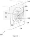
- FIG. 1 shows the outer components of an exemplary capacitor 100, for use with a capacitor header, as well as components of a capacitor header in accordance with an embodiment of the present invention.
- the capacitor 100 may be charged to generate a large potential difference between the two capacitor plates.
- the capacitor 100 comprises a metal outer casing 102 connected to an earth.
- the outer casing 102 is conductively connected to a conductive metal ground ring 104 that is integral to the outer casing 102 of the capacitor 100.
- the ground ring 104 is conductively connected to an internal ground conductor (not shown) of the capacitor 100.
- the capacitor 100 also comprises a metal central live conductor 106 (that has formed therein a threaded central aperture for receiving a bolt) for connecting to a live output plate of the capacitor header (as will be shown in Figures 2 and 3 ).
- Figure 1 also shows a first insulating member 108 (of a capacitor header in accordance with an embodiment of the present invention) located within an aperture defined by the annular ground ring 104.
- the first insulating member 108 is also annular and is arranged coaxially with the ground ring 104 and the central live conductor 106 of the capacitor 100.
- the first insulating member 108 comprises a central aperture in which the central live conductor 106 is located. As will be shown in Figures 2 and 3 , the central live conductor 106 is arranged to be connected to the live output plate of the capacitor header.
- the first insulating member 108 also comprises three concentric projecting walls 112 and two recessed channels 114 defined between the projecting walls 112. The projecting walls 112 and recessed channels 114 have a square stepped cross section in the radial direction.
- the capacitor 100 shown in Figure 1 comprises a capacitor header for coupling the output voltage from the capacitor.
- Figure 2 shows an exploded view of a capacitor header according to an embodiment of the present invention for use with the capacitor 100 shown in Figure 1 .
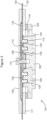
- Figure 3 shows a cross-sectional view of the capacitor header 101 shown in
- FIG. 2 (and some of the parts thereof in Figure 1 ). A number of the components of the capacitor header 101 are shown with the capacitor 100 in Figure 1 .
- the capacitor header 101 includes a ground output plate 117, which is conductively connected to the ground conductor of the capacitor 100 via a metal annular spacer ring 116 and the ground ring 104 of the outer casing 102 of the capacitor 100.
- the spacer ring 116 and the ground ring 104 each have an inner diameter that is the same as the inner diameter of the ground output plate 117 but each have a smaller outer diameter than the ground output plate 117.
- the ground ring 104 and the first insulating member 108 are not shown in Figure 2 .
- the capacitor header 101 also includes a metal live output plate 120, which is conductively connected to the live conductor 106 of the capacitor via a conductive metal collar 110 and a conductive metal retaining bolt 122 that passes through a central aperture in the live output plate 120 and screws into the conductive collar 110 and the live conductor 106.
- the ground and live output plates 117, 120 thus form a pair of transmission lines for discharging the capacitor 100.
- the live conductor 106 engages with the underside of the first insulating member 108 (which thus forms part of the capacitor header 101) to clamp the components of the capacitor header 101 together between the live output plate 120 and the first insulating member 108.
- the conductive collar 110 sits between the live conductor 106 and the live output plate 120, and thus conductively connects the central live conductor 106 of the capacitor 100 to the live output plate 120 via the conductive retaining bolt 122.
- a step on the outer diameter of the first insulating member 108 engages with a step on the inner diameter of the ground ring 104.
- the three concentric projecting walls 112 and two recessed channels 114 of the first insulating member 108 interleave with an annular second insulating member 124 of the capacitor header 101.
- the second insulating member 124 has a central aperture, as well as two concentric projecting walls 126 and three recessed channels 128 that are complementary to (i.e. have the same shape and dimensions as) the three concentric projecting walls 112 and two recessed channels 114 of the first insulating member 108 such that they define a castellated path between them.
- the second insulating member 124 has an outer portion that extends between the live output plate 120 and the ground output plate 117.
- the live output plate 120 has a recess in its face that is adjacent the second insulating member 124 to accommodate the second insulating member 124. An outer edge portion of the live output plate 120 then steps back towards the ground output plate 117.
- the first insulating member 108 and the second insulating member 124 are each formed from polyoxymethylene (acetal).
- Three concentric annular sealing rings 129 are located in the three recessed channels 128 of the second insulating member 124.
- Each sealing ring 129 has a greater thickness than the sealing ring 129 radially inside it, in order to account for the clamping of the capacitor header 101 at the centre by the retaining bolt 122.
- the sealing rings 129 are therefore compressed between the three recessed channels 128 of the second insulating member 124 and the respective three concentric projecting walls 112 of the first insulating member 108.
- a further annular seal 130 is located in a recess in the other side of the second insulating member 124.
- the capacitor header 101 also includes first and second sets of insulating sheets 132, 134.
- the first and second sets of insulating sheets 132, 134 each have twenty sheets formed from boPET, e.g. Mylar (RTM), with each sheet having a thickness of 75 microns.
- RTM Mylar
- the first and second sets of insulating sheets 132, 134 extend further outwards from the capacitor header 101 and each set is bent away from the plane in which they are shown in Figure 3 .
- the first set of insulating sheets 132 extends between the live and ground output plates 120, 117, between the ground output plate 117 and the second insulating member 124, and between the outer sealing ring 129 and the recessed channel 128 of the second insulating member 124.
- the inner diameter of the first set of insulating sheets 132 coincides with the outer diameter of the outermost of the two projecting walls 126 of the second insulating member 124.
- the second set of insulating sheets 134 extends between the live and ground output plates 120, 117, and between the live output plate 120 and the second insulating member 124.
- the inner diameter of the second set of insulating sheets 134 coincides with the inner diameter of the second insulating member 124.
- the second set of insulating sheets 134 thus extends across the further annular seal 130, between the annular seal 130 and the live output plate 120.
- the capacitor 100 and the capacitor header 101 are assembled as shown in Figures 1 and 3 .
- the components of the capacitor header 101 are clamped together between the retaining bolt 122 and the live conductor 106. This acts both to retain the components of the capacitor header 101 together and to conductively connect the live output plate 120 of the capacitor header 101 with the central live conductor 106 of the capacitor 100.
- the force exerted by the retaining bolt 122 acts to compress the three concentric annular sealing rings 129 between the three recessed channels 128 of the second insulating member 124 and the respective three concentric projecting walls 112 of the first insulating member 108.
- the further annular seal 130 is also compressed between the second insulating member 124 and the second set of insulating sheets 134.
- the internal capacitor plates (connected to the central live conductor 106 and the ground conductor of the capacitor 100 respectively) are charged over a period of time to a high potential difference. Owing to the conductive connections to the ground and live output plates 117, 120, a large potential difference is formed between the ground and live output plates 117, 120.
- the insulating components of the capacitor header 101 prevent dielectric breakdown, e.g. via surface tracking or corona discharge. This allows the potential difference to be held for a relatively long period of time while the capacitor is being charged.
- the first is around the edges of the first and second sets of insulating sheets 132, 134.
- the first and second sets of insulating sheets 132, 134 extend significantly beyond the outer diameter of the ground and live output plates 117, 120, and they are also bent away from the plane shown in Figure 3 . This has the effect of increasing the path length between the ground and live output plates 117, 120 around the first and second sets of insulating sheets 132, 134, which helps to reduce the risk of surface tracking along this path.
- first and second sets of insulating sheets 132, 134 (comprising forty sheets of Mylar) between the ground and live output plates 117, 120 reduce the risk of electrical punch-through and thus direct dielectric breakdown of the first and second sets of insulating sheets 132, 134.
- a second path between the ground and live output plates 117, 120 exists from the ground output plate 117 along the path between the first and second insulating members 108, 124.
- a number of features make it difficult for surface tracking and corona breakdown to occur along this path.
- the interleaving concentric projecting walls 112, 126 and recessed channels 114, 128 of the first and second insulating members 108, 124 create a highly tortuous castellated path between the ground and live output plates 117, 120, thus helping to reduce the risk of surface tracking along this path.
- the compression of the annular sealing rings 129 and the further annular seal 130 helps to expel air from the capacitor header 101, in particular from the path between the ground and live output plates 117, 120.
- annular sealing rings 129 This helps to reduce the risk of corona breakdown.
- a doping agent e.g. zinc oxide
- first and second insulating members 108, 124 and the first and second sets of insulating sheets 132, 134 while providing relatively long path lengths between the ground and live output plates 117, 120, allows the ground and live output plates 117, 120 to be brought close together in the capacitor header 101. This helps to reduce the inductance of the capacitor header, such that the capacitor may be discharged relatively quickly.
- the capacitor and capacitor header of the present invention allow the capacitor to store a large amount of charge and then discharge this as a high voltage and current pulse rapidly from the capacitor, while reducing the risk of dielectric breakdown.
Landscapes
- Engineering & Computer Science (AREA)
- Power Engineering (AREA)
- Microelectronics & Electronic Packaging (AREA)
- Manufacturing & Machinery (AREA)
- Fixed Capacitors And Capacitor Manufacturing Machines (AREA)
- Measuring Oxygen Concentration In Cells (AREA)
- Electric Double-Layer Capacitors Or The Like (AREA)
- X-Ray Techniques (AREA)
Claims (15)
- Kondensator-Abschlussscheibe (101) zum Koppeln eines Spannungsausgangs von einem Kondensator (100), wobei die Kondensator-Abschlussscheibe gekennzeichnet ist durch:eine stromführende Ausgangsplatte (120) zur elektrischen Verbindung mit einem zentralen stromführenden Leiter (106) des Kondensators;eine Erdungsausgangsplatte (117) zur elektrischen Verbindung mit einem Erdungsleiter des Kondensators, wobei die Erdungsausgangsplatte eine Öffnung umfasst, die eine Verbindung zwischen der stromführenden Ausgangsplatte und dem zentralen stromführenden Leiter ermöglicht;ein erstes Isolierelement (108) und ein zweites Isolierelement (124), die jeweils zumindest teilweise innerhalb der Öffnung der Erdungsausgangsplatte angeordnet sind, wobei sowohl das erste Isolierelement als auch das zweite Isolierelement eine Öffnung umfasst, die eine Verbindung zwischen der stromführenden Ausgangsplatte und dem zentralen stromführenden Leiter ermöglicht, wobei sowohl das erste Isolierelement als auch das zweite Isolierelement eine nicht-planare Passfläche umfasst und wobei die nicht-planaren Passflächen des ersten Isolierelements und des zweiten Isolierelements ineinandergreifen, um einen nicht-linearen Pfad zwischen der Erdungsausgangsplatte und den Öffnungen in dem ersten Isolierelement und dem zweiten Isolierelement zu bilden;mindestens eine Isolierdichtung (129) zwischen den nicht-planaren Passflächen des ersten Isolierelements und des zweiten Isolierelements;einen ersten Satz aus einer oder mehreren Isolierschichten (132) zwischen der Erdungsausgangsplatte und dem zweiten Isolierelement; undeinen zweiten Satz aus einer oder mehreren Isolierschichten (134) zwischen der stromführenden Ausgangsplatte und dem zweiten Isolierelement;wobei sich der erste Satz aus einer oder mehreren Isolierschichten und der zweite Satz aus einer oder mehreren Isolierschichten über einen Außenumfang der stromführenden Ausgangsplatte und der Erdungsausgangsplatte hinaus erstrecken.
- Kondensator-Abschlussscheibe nach Anspruch 1, wobei die Kondensator-Abschlussscheibe (101) rotationssymmetrisch um eine Achse durch die Öffnungen des ersten und des zweiten Isolierelements (108, 124) ist.
- Kondensator-Abschlussscheibe nach Anspruch 1 oder 2, wobei die Kondensator-Abschlussscheibe (101) einen leitenden Verbinder umfasst, der zur elektrischen Verbindung mit einem zentralen stromführenden Leiter (106) des Kondensators elektrisch mit der stromführenden Ausgangsplatte (120) verbunden ist.
- Kondensator-Abschlussscheibe (101) nach einem der vorstehenden Ansprüche, wobei die stromführende Ausgangsplatte (120) eine zentrale Öffnung umfasst, wobei eine Außenabmessung der Öffnung der Erdungsausgangsplatte (117) größer als eine Außenabmessung der Öffnung der stromführenden Ausgangsplatte ist.
- Kondensator-Abschlussscheibe (101) nach einem der vorstehenden Ansprüche, wobei eine Außenabmessung des ersten Isolierelements (108) kleiner oder gleich einer Innenabmessung der Erdungsausgangsplatte (117) ist.
- Kondensator-Abschlussscheibe (101) nach einem der vorstehenden Ansprüche, wobei die nicht-planare Passfläche des ersten Isolierelements (108) komplementär zu der nicht-planaren Passfläche des zweiten Isolierelements (124) ist.
- Kondensator-Abschlussscheibe (101) nach einem der vorstehenden Ansprüche, wobei die nicht-planaren Passflächen eine oder mehrere vorstehende Wände (112) und vertiefte Kanäle (114) umfassen, die sich azimutal erstrecken.
- Kondensator-Abschlussscheibe (101) nach einem der vorstehenden Ansprüche, wobei die Kondensator-Abschlussscheibe eine Vielzahl von Isolierdichtungen umfasst und wobei eine der Vielzahl von Isolierdichtungen, die näher an der Erdungsausgangsplatte (117) liegen, eine Dicke aufweist, die größer als eine Dicke einer anderen der Vielzahl von Isolierdichtungen ist, die näher an den Öffnungen des ersten und des zweiten Isolierelements (108, 124) liegen.
- Kondensator-Abschlussscheibe (101) nach einem der vorstehenden Ansprüche, wobei die mindestens eine Isolierdichtung Silikon umfasst.
- Kondensator-Abschlussscheibe (101) nach einem der vorstehenden Ansprüche, wobei sich der erste Satz aus einer oder mehreren Isolierschichten (132) zwischen dem ersten Isolierelement (108) und dem zweiten Isolierelement (124) erstreckt.
- Kondensator-Abschlussscheibe (101) nach einem der vorstehenden Ansprüche, wobei eine Innenabmessung des ersten Satzes aus einer oder mehreren Isolierschichten (132) geringer ist als eine Innenabmessung der Erdungsausgangsplatte (117) und/oder geringer ist als eine Außenabmessung des ersten Isolierelements (108).
- Kondensator-Abschlussscheibe (101) nach einem der vorstehenden Ansprüche, wobei die Kondensator-Abschlussscheibe eine zusätzliche Isolierdichtung zwischen dem zweiten Isolierelement (124) und der stromführenden Ausgangsplatte (120) umfasst.
- Kondensator-Abschlussscheibe (101) nach einem der vorstehenden Ansprüche, wobei ein äußerer Abschnitt des ersten und/oder zweiten Satzes aus Isolierschichten (132, 134) gekrümmt ist.
- Kondensator-Abschlussscheibe (101) nach einem der vorstehenden Ansprüche, wobei jede der einen oder mehreren Isolierschichten in dem ersten und dem zweiten Satz (132, 134) aus einer oder mehreren Isolierschichten eine Dicke von weniger als 200 Mikrometern aufweist, z. B. weniger als 100 Mikrometer, z. B. etwa 75 Mikrometer.
- Kondensator (100) zum Speichern elektrischer Ladung, wobei der Kondensator umfasst:einen äußeren Erdungsleiter;einen zentralen stromführenden Leiter (106); undeine Kondensator-Abschlussscheibe (101) nach Anspruch 1 zum Koppeln eines Spannungsausgangs eines Kondensators, wobeidie Erdungsausgangsplatte (117) eine Öffnung umfasst, durch die sich der zentrale stromführende Leiter oder ein Verbinder zwischen dem zentralen stromführenden Leiter und der stromführenden Ausgangsplatte (120) erstreckt; undwobei sowohl das erste Isolierelement (108) als auch das zweite Isolierelement (124) eine Öffnung umfasst, durch die sich der zentrale stromführende Leiter oder ein Verbinder zwischen dem zentralen stromführenden Leiter und der stromführenden Ausgangsplatte erstreckt.
Applications Claiming Priority (2)
| Application Number | Priority Date | Filing Date | Title |
|---|---|---|---|
| GB2001050.0A GB2579465B (en) | 2020-01-24 | 2020-01-24 | Capacitor Header |
| PCT/GB2021/050143 WO2021148799A1 (en) | 2020-01-24 | 2021-01-22 | Capacitor header |
Publications (2)
| Publication Number | Publication Date |
|---|---|
| EP4094279A1 EP4094279A1 (de) | 2022-11-30 |
| EP4094279B1 true EP4094279B1 (de) | 2024-04-03 |
Family
ID=69725999
Family Applications (1)
| Application Number | Title | Priority Date | Filing Date |
|---|---|---|---|
| EP21702077.5A Active EP4094279B1 (de) | 2020-01-24 | 2021-01-22 | Abschlussscheibe für kondensator |
Country Status (5)
| Country | Link |
|---|---|
| US (1) | US12205767B2 (de) |
| EP (1) | EP4094279B1 (de) |
| CN (1) | CN115004327B (de) |
| GB (1) | GB2579465B (de) |
| WO (1) | WO2021148799A1 (de) |
Family Cites Families (12)
| Publication number | Priority date | Publication date | Assignee | Title |
|---|---|---|---|---|
| DE4426927A1 (de) | 1994-07-29 | 1996-02-01 | Hoechst Ceram Tec Ag | Elektrischer Isolator aus Silikongummi für Hochspannungsanwendungen |
| US6282078B1 (en) * | 2000-04-19 | 2001-08-28 | Real Power Cap Company | Capacitor for car stereo with current distributing capability |
| US6567259B2 (en) * | 2001-05-31 | 2003-05-20 | Greatbatch-Sierra, Inc. | Monolithic ceramic capacitor with barium titinate dielectric curie point optimized for active implantable medical devices operating at 37° C. |
| JP2005109006A (ja) | 2003-09-29 | 2005-04-21 | Tdk Corp | 高電圧貫通型コンデンサ及びマグネトロン |
| US9412521B2 (en) * | 2005-04-07 | 2016-08-09 | American Radionic Company, Inc. | Capacitor with multiple elements for multiple replacement applications |
| JP4877994B2 (ja) | 2007-03-14 | 2012-02-15 | 日立エーアイシー株式会社 | 電解コンデンサ |
| KR101049282B1 (ko) * | 2009-03-03 | 2011-07-13 | 주식회사 네스캡 | 전기에너지 저장장치 |
| US8259435B2 (en) | 2010-11-01 | 2012-09-04 | Avx Corporation | Hermetically sealed wet electrolytic capacitor |
| CN105793937B (zh) | 2013-12-03 | 2020-09-15 | Abb电网瑞士股份公司 | 多层电介质聚合物材料、电容器、材料用途及其形成方法 |
| CN105304323B (zh) * | 2015-11-30 | 2017-12-01 | 中国西电电气股份有限公司 | 一种具有插拔式双极出线结构的高压电容器 |
| CN205140752U (zh) | 2015-12-09 | 2016-04-06 | 广东顺容电气有限公司 | 一种电容器用接线端子 |
| CN209087592U (zh) * | 2018-10-23 | 2019-07-09 | 上海琪瑜光电科技股份有限公司 | 电容器绝缘端子及高压脉冲电容器 |
-
2020
- 2020-01-24 GB GB2001050.0A patent/GB2579465B/en not_active Expired - Fee Related
-
2021
- 2021-01-22 US US17/794,477 patent/US12205767B2/en active Active
- 2021-01-22 CN CN202180010694.5A patent/CN115004327B/zh active Active
- 2021-01-22 EP EP21702077.5A patent/EP4094279B1/de active Active
- 2021-01-22 WO PCT/GB2021/050143 patent/WO2021148799A1/en not_active Ceased
Also Published As
| Publication number | Publication date |
|---|---|
| CN115004327B (zh) | 2024-10-25 |
| CN115004327A (zh) | 2022-09-02 |
| US20230060632A1 (en) | 2023-03-02 |
| EP4094279A1 (de) | 2022-11-30 |
| GB202001050D0 (en) | 2020-03-11 |
| GB2579465B (en) | 2021-05-05 |
| US12205767B2 (en) | 2025-01-21 |
| GB2579465A8 (en) | 2020-12-16 |
| GB2579465A (en) | 2020-06-24 |
| WO2021148799A1 (en) | 2021-07-29 |
Similar Documents
| Publication | Publication Date | Title |
|---|---|---|
| US12183957B2 (en) | Assembled structure of pole and pole current collector disk, and battery | |
| EP2317587B1 (de) | Wiederaufladbare Batterie | |
| US9299972B2 (en) | Rechargeable battery with separating member between current collector and battery case | |
| EP3188280B1 (de) | Deckelanordnung und sekundärbatterie damit | |
| US20090123820A1 (en) | Battery module | |
| KR101679413B1 (ko) | 중공형 이차전지 | |
| CN101390243B (zh) | 具有电极支撑元件的电极组件以及包括该电极组件的二次电池 | |
| KR101530803B1 (ko) | 이차 전지 | |
| EP2597704A2 (de) | Sekundärbatterie mit einer differential-leitstruktur | |
| TW201230104A (en) | High voltage electric double layer capacitor device and methods of manufacture | |
| US12205767B2 (en) | Capacitor header | |
| US8993139B2 (en) | Sealed secondary battery | |
| JP6252817B2 (ja) | 蓄電装置 | |
| KR20190136202A (ko) | 과충전을 방지하기 위한 원통형 이차전지 | |
| CN112216934A (zh) | 电池盖板组件及单体电池 | |
| KR20180109522A (ko) | 전기 에너지 저장용 축전장치와 그 연결체 및 이를 포함하는 직렬 연결구조 | |
| EP2772962A2 (de) | Wiederaufladbare Batterie | |
| CA2456474C (en) | Active part for a surge arrester | |
| EP3217455A1 (de) | Elektrodenanordnung und batteriezelle | |
| EP4094331B1 (de) | Elektrische schaltungsanordnung | |
| EP3358644B1 (de) | Batteriezelle und batteriemodul | |
| US5302473A (en) | Current collector for electrochemical device | |
| JP2740390B2 (ja) | 酸化亜鉛形避雷器 | |
| JP2011060491A (ja) | 絶縁操作ロッド | |
| CN121355490B (zh) | 盖板组件、电芯及用电设备 |
Legal Events
| Date | Code | Title | Description |
|---|---|---|---|
| STAA | Information on the status of an ep patent application or granted ep patent |
Free format text: STATUS: UNKNOWN |
|
| STAA | Information on the status of an ep patent application or granted ep patent |
Free format text: STATUS: THE INTERNATIONAL PUBLICATION HAS BEEN MADE |
|
| PUAI | Public reference made under article 153(3) epc to a published international application that has entered the european phase |
Free format text: ORIGINAL CODE: 0009012 |
|
| STAA | Information on the status of an ep patent application or granted ep patent |
Free format text: STATUS: REQUEST FOR EXAMINATION WAS MADE |
|
| 17P | Request for examination filed |
Effective date: 20220823 |
|
| AK | Designated contracting states |
Kind code of ref document: A1 Designated state(s): AL AT BE BG CH CY CZ DE DK EE ES FI FR GB GR HR HU IE IS IT LI LT LU LV MC MK MT NL NO PL PT RO RS SE SI SK SM TR |
|
| DAV | Request for validation of the european patent (deleted) | ||
| DAX | Request for extension of the european patent (deleted) | ||
| STAA | Information on the status of an ep patent application or granted ep patent |
Free format text: STATUS: EXAMINATION IS IN PROGRESS |
|
| 17Q | First examination report despatched |
Effective date: 20230801 |
|
| GRAP | Despatch of communication of intention to grant a patent |
Free format text: ORIGINAL CODE: EPIDOSNIGR1 |
|
| STAA | Information on the status of an ep patent application or granted ep patent |
Free format text: STATUS: GRANT OF PATENT IS INTENDED |
|
| GRAS | Grant fee paid |
Free format text: ORIGINAL CODE: EPIDOSNIGR3 |
|
| INTG | Intention to grant announced |
Effective date: 20240125 |
|
| GRAA | (expected) grant |
Free format text: ORIGINAL CODE: 0009210 |
|
| STAA | Information on the status of an ep patent application or granted ep patent |
Free format text: STATUS: THE PATENT HAS BEEN GRANTED |
|
| AK | Designated contracting states |
Kind code of ref document: B1 Designated state(s): AL AT BE BG CH CY CZ DE DK EE ES FI FR GB GR HR HU IE IS IT LI LT LU LV MC MK MT NL NO PL PT RO RS SE SI SK SM TR |
|
| REG | Reference to a national code |
Ref country code: CH Ref legal event code: EP |
|
| REG | Reference to a national code |
Ref country code: IE Ref legal event code: FG4D |
|
| REG | Reference to a national code |
Ref country code: DE Ref legal event code: R096 Ref document number: 602021011255 Country of ref document: DE |
|
| REG | Reference to a national code |
Ref country code: LT Ref legal event code: MG9D |
|
| REG | Reference to a national code |
Ref country code: NL Ref legal event code: MP Effective date: 20240403 |
|
| REG | Reference to a national code |
Ref country code: AT Ref legal event code: MK05 Ref document number: 1673315 Country of ref document: AT Kind code of ref document: T Effective date: 20240403 |
|
| PG25 | Lapsed in a contracting state [announced via postgrant information from national office to epo] |
Ref country code: NL Free format text: LAPSE BECAUSE OF FAILURE TO SUBMIT A TRANSLATION OF THE DESCRIPTION OR TO PAY THE FEE WITHIN THE PRESCRIBED TIME-LIMIT Effective date: 20240403 |
|
| PG25 | Lapsed in a contracting state [announced via postgrant information from national office to epo] |
Ref country code: NL Free format text: LAPSE BECAUSE OF FAILURE TO SUBMIT A TRANSLATION OF THE DESCRIPTION OR TO PAY THE FEE WITHIN THE PRESCRIBED TIME-LIMIT Effective date: 20240403 |
|
| PG25 | Lapsed in a contracting state [announced via postgrant information from national office to epo] |
Ref country code: IS Free format text: LAPSE BECAUSE OF FAILURE TO SUBMIT A TRANSLATION OF THE DESCRIPTION OR TO PAY THE FEE WITHIN THE PRESCRIBED TIME-LIMIT Effective date: 20240803 |
|
| PG25 | Lapsed in a contracting state [announced via postgrant information from national office to epo] |
Ref country code: BG Free format text: LAPSE BECAUSE OF FAILURE TO SUBMIT A TRANSLATION OF THE DESCRIPTION OR TO PAY THE FEE WITHIN THE PRESCRIBED TIME-LIMIT Effective date: 20240403 |
|
| PG25 | Lapsed in a contracting state [announced via postgrant information from national office to epo] |
Ref country code: FI Free format text: LAPSE BECAUSE OF FAILURE TO SUBMIT A TRANSLATION OF THE DESCRIPTION OR TO PAY THE FEE WITHIN THE PRESCRIBED TIME-LIMIT Effective date: 20240403 Ref country code: HR Free format text: LAPSE BECAUSE OF FAILURE TO SUBMIT A TRANSLATION OF THE DESCRIPTION OR TO PAY THE FEE WITHIN THE PRESCRIBED TIME-LIMIT Effective date: 20240403 |
|
| PG25 | Lapsed in a contracting state [announced via postgrant information from national office to epo] |
Ref country code: GR Free format text: LAPSE BECAUSE OF FAILURE TO SUBMIT A TRANSLATION OF THE DESCRIPTION OR TO PAY THE FEE WITHIN THE PRESCRIBED TIME-LIMIT Effective date: 20240704 |
|
| PG25 | Lapsed in a contracting state [announced via postgrant information from national office to epo] |
Ref country code: PT Free format text: LAPSE BECAUSE OF FAILURE TO SUBMIT A TRANSLATION OF THE DESCRIPTION OR TO PAY THE FEE WITHIN THE PRESCRIBED TIME-LIMIT Effective date: 20240805 |
|
| PG25 | Lapsed in a contracting state [announced via postgrant information from national office to epo] |
Ref country code: ES Free format text: LAPSE BECAUSE OF FAILURE TO SUBMIT A TRANSLATION OF THE DESCRIPTION OR TO PAY THE FEE WITHIN THE PRESCRIBED TIME-LIMIT Effective date: 20240403 |
|
| PG25 | Lapsed in a contracting state [announced via postgrant information from national office to epo] |
Ref country code: CZ Free format text: LAPSE BECAUSE OF FAILURE TO SUBMIT A TRANSLATION OF THE DESCRIPTION OR TO PAY THE FEE WITHIN THE PRESCRIBED TIME-LIMIT Effective date: 20240403 |
|
| PG25 | Lapsed in a contracting state [announced via postgrant information from national office to epo] |
Ref country code: AT Free format text: LAPSE BECAUSE OF FAILURE TO SUBMIT A TRANSLATION OF THE DESCRIPTION OR TO PAY THE FEE WITHIN THE PRESCRIBED TIME-LIMIT Effective date: 20240403 |
|
| PG25 | Lapsed in a contracting state [announced via postgrant information from national office to epo] |
Ref country code: PL Free format text: LAPSE BECAUSE OF FAILURE TO SUBMIT A TRANSLATION OF THE DESCRIPTION OR TO PAY THE FEE WITHIN THE PRESCRIBED TIME-LIMIT Effective date: 20240403 |
|
| PG25 | Lapsed in a contracting state [announced via postgrant information from national office to epo] |
Ref country code: LV Free format text: LAPSE BECAUSE OF FAILURE TO SUBMIT A TRANSLATION OF THE DESCRIPTION OR TO PAY THE FEE WITHIN THE PRESCRIBED TIME-LIMIT Effective date: 20240403 |
|
| PG25 | Lapsed in a contracting state [announced via postgrant information from national office to epo] |
Ref country code: PT Free format text: LAPSE BECAUSE OF FAILURE TO SUBMIT A TRANSLATION OF THE DESCRIPTION OR TO PAY THE FEE WITHIN THE PRESCRIBED TIME-LIMIT Effective date: 20240805 Ref country code: PL Free format text: LAPSE BECAUSE OF FAILURE TO SUBMIT A TRANSLATION OF THE DESCRIPTION OR TO PAY THE FEE WITHIN THE PRESCRIBED TIME-LIMIT Effective date: 20240403 Ref country code: NO Free format text: LAPSE BECAUSE OF FAILURE TO SUBMIT A TRANSLATION OF THE DESCRIPTION OR TO PAY THE FEE WITHIN THE PRESCRIBED TIME-LIMIT Effective date: 20240703 Ref country code: LV Free format text: LAPSE BECAUSE OF FAILURE TO SUBMIT A TRANSLATION OF THE DESCRIPTION OR TO PAY THE FEE WITHIN THE PRESCRIBED TIME-LIMIT Effective date: 20240403 Ref country code: IS Free format text: LAPSE BECAUSE OF FAILURE TO SUBMIT A TRANSLATION OF THE DESCRIPTION OR TO PAY THE FEE WITHIN THE PRESCRIBED TIME-LIMIT Effective date: 20240803 Ref country code: HR Free format text: LAPSE BECAUSE OF FAILURE TO SUBMIT A TRANSLATION OF THE DESCRIPTION OR TO PAY THE FEE WITHIN THE PRESCRIBED TIME-LIMIT Effective date: 20240403 Ref country code: GR Free format text: LAPSE BECAUSE OF FAILURE TO SUBMIT A TRANSLATION OF THE DESCRIPTION OR TO PAY THE FEE WITHIN THE PRESCRIBED TIME-LIMIT Effective date: 20240704 Ref country code: FI Free format text: LAPSE BECAUSE OF FAILURE TO SUBMIT A TRANSLATION OF THE DESCRIPTION OR TO PAY THE FEE WITHIN THE PRESCRIBED TIME-LIMIT Effective date: 20240403 Ref country code: ES Free format text: LAPSE BECAUSE OF FAILURE TO SUBMIT A TRANSLATION OF THE DESCRIPTION OR TO PAY THE FEE WITHIN THE PRESCRIBED TIME-LIMIT Effective date: 20240403 Ref country code: CZ Free format text: LAPSE BECAUSE OF FAILURE TO SUBMIT A TRANSLATION OF THE DESCRIPTION OR TO PAY THE FEE WITHIN THE PRESCRIBED TIME-LIMIT Effective date: 20240403 Ref country code: BG Free format text: LAPSE BECAUSE OF FAILURE TO SUBMIT A TRANSLATION OF THE DESCRIPTION OR TO PAY THE FEE WITHIN THE PRESCRIBED TIME-LIMIT Effective date: 20240403 Ref country code: AT Free format text: LAPSE BECAUSE OF FAILURE TO SUBMIT A TRANSLATION OF THE DESCRIPTION OR TO PAY THE FEE WITHIN THE PRESCRIBED TIME-LIMIT Effective date: 20240403 Ref country code: RS Free format text: LAPSE BECAUSE OF FAILURE TO SUBMIT A TRANSLATION OF THE DESCRIPTION OR TO PAY THE FEE WITHIN THE PRESCRIBED TIME-LIMIT Effective date: 20240703 |
|
| REG | Reference to a national code |
Ref country code: DE Ref legal event code: R097 Ref document number: 602021011255 Country of ref document: DE |
|
| PG25 | Lapsed in a contracting state [announced via postgrant information from national office to epo] |
Ref country code: DK Free format text: LAPSE BECAUSE OF FAILURE TO SUBMIT A TRANSLATION OF THE DESCRIPTION OR TO PAY THE FEE WITHIN THE PRESCRIBED TIME-LIMIT Effective date: 20240403 |
|
| PG25 | Lapsed in a contracting state [announced via postgrant information from national office to epo] |
Ref country code: EE Free format text: LAPSE BECAUSE OF FAILURE TO SUBMIT A TRANSLATION OF THE DESCRIPTION OR TO PAY THE FEE WITHIN THE PRESCRIBED TIME-LIMIT Effective date: 20240403 |
|
| PG25 | Lapsed in a contracting state [announced via postgrant information from national office to epo] |
Ref country code: SK Free format text: LAPSE BECAUSE OF FAILURE TO SUBMIT A TRANSLATION OF THE DESCRIPTION OR TO PAY THE FEE WITHIN THE PRESCRIBED TIME-LIMIT Effective date: 20240403 Ref country code: RO Free format text: LAPSE BECAUSE OF FAILURE TO SUBMIT A TRANSLATION OF THE DESCRIPTION OR TO PAY THE FEE WITHIN THE PRESCRIBED TIME-LIMIT Effective date: 20240403 |
|
| PG25 | Lapsed in a contracting state [announced via postgrant information from national office to epo] |
Ref country code: SM Free format text: LAPSE BECAUSE OF FAILURE TO SUBMIT A TRANSLATION OF THE DESCRIPTION OR TO PAY THE FEE WITHIN THE PRESCRIBED TIME-LIMIT Effective date: 20240403 |
|
| PG25 | Lapsed in a contracting state [announced via postgrant information from national office to epo] |
Ref country code: SM Free format text: LAPSE BECAUSE OF FAILURE TO SUBMIT A TRANSLATION OF THE DESCRIPTION OR TO PAY THE FEE WITHIN THE PRESCRIBED TIME-LIMIT Effective date: 20240403 Ref country code: SK Free format text: LAPSE BECAUSE OF FAILURE TO SUBMIT A TRANSLATION OF THE DESCRIPTION OR TO PAY THE FEE WITHIN THE PRESCRIBED TIME-LIMIT Effective date: 20240403 Ref country code: RO Free format text: LAPSE BECAUSE OF FAILURE TO SUBMIT A TRANSLATION OF THE DESCRIPTION OR TO PAY THE FEE WITHIN THE PRESCRIBED TIME-LIMIT Effective date: 20240403 Ref country code: EE Free format text: LAPSE BECAUSE OF FAILURE TO SUBMIT A TRANSLATION OF THE DESCRIPTION OR TO PAY THE FEE WITHIN THE PRESCRIBED TIME-LIMIT Effective date: 20240403 Ref country code: DK Free format text: LAPSE BECAUSE OF FAILURE TO SUBMIT A TRANSLATION OF THE DESCRIPTION OR TO PAY THE FEE WITHIN THE PRESCRIBED TIME-LIMIT Effective date: 20240403 |
|
| PLBE | No opposition filed within time limit |
Free format text: ORIGINAL CODE: 0009261 |
|
| STAA | Information on the status of an ep patent application or granted ep patent |
Free format text: STATUS: NO OPPOSITION FILED WITHIN TIME LIMIT |
|
| 26N | No opposition filed |
Effective date: 20250106 |
|
| PG25 | Lapsed in a contracting state [announced via postgrant information from national office to epo] |
Ref country code: SI Free format text: LAPSE BECAUSE OF FAILURE TO SUBMIT A TRANSLATION OF THE DESCRIPTION OR TO PAY THE FEE WITHIN THE PRESCRIBED TIME-LIMIT Effective date: 20240403 |
|
| REG | Reference to a national code |
Ref country code: CH Ref legal event code: PL |
|
| PG25 | Lapsed in a contracting state [announced via postgrant information from national office to epo] |
Ref country code: SE Free format text: LAPSE BECAUSE OF FAILURE TO SUBMIT A TRANSLATION OF THE DESCRIPTION OR TO PAY THE FEE WITHIN THE PRESCRIBED TIME-LIMIT Effective date: 20240403 |
|
| PG25 | Lapsed in a contracting state [announced via postgrant information from national office to epo] |
Ref country code: MC Free format text: LAPSE BECAUSE OF FAILURE TO SUBMIT A TRANSLATION OF THE DESCRIPTION OR TO PAY THE FEE WITHIN THE PRESCRIBED TIME-LIMIT Effective date: 20240403 Ref country code: LU Free format text: LAPSE BECAUSE OF NON-PAYMENT OF DUE FEES Effective date: 20250122 |
|
| PG25 | Lapsed in a contracting state [announced via postgrant information from national office to epo] |
Ref country code: BE Free format text: LAPSE BECAUSE OF NON-PAYMENT OF DUE FEES Effective date: 20250131 |
|
| PG25 | Lapsed in a contracting state [announced via postgrant information from national office to epo] |
Ref country code: CH Free format text: LAPSE BECAUSE OF NON-PAYMENT OF DUE FEES Effective date: 20250131 |
|
| REG | Reference to a national code |
Ref country code: BE Ref legal event code: MM Effective date: 20250131 |
|
| PG25 | Lapsed in a contracting state [announced via postgrant information from national office to epo] |
Ref country code: IE Free format text: LAPSE BECAUSE OF NON-PAYMENT OF DUE FEES Effective date: 20250122 |
|
| PG25 | Lapsed in a contracting state [announced via postgrant information from national office to epo] |
Ref country code: IT Free format text: LAPSE BECAUSE OF FAILURE TO SUBMIT A TRANSLATION OF THE DESCRIPTION OR TO PAY THE FEE WITHIN THE PRESCRIBED TIME-LIMIT Effective date: 20240403 |
|
| PGFP | Annual fee paid to national office [announced via postgrant information from national office to epo] |
Ref country code: GB Payment date: 20260120 Year of fee payment: 6 |
|
| PGFP | Annual fee paid to national office [announced via postgrant information from national office to epo] |
Ref country code: DE Payment date: 20260122 Year of fee payment: 6 |
|
| PGFP | Annual fee paid to national office [announced via postgrant information from national office to epo] |
Ref country code: FR Payment date: 20260121 Year of fee payment: 6 |