EP4087233B1 - Vorrichtung für optische kohärenztomografie - Google Patents
Vorrichtung für optische kohärenztomografie Download PDFInfo
- Publication number
- EP4087233B1 EP4087233B1 EP21757783.2A EP21757783A EP4087233B1 EP 4087233 B1 EP4087233 B1 EP 4087233B1 EP 21757783 A EP21757783 A EP 21757783A EP 4087233 B1 EP4087233 B1 EP 4087233B1
- Authority
- EP
- European Patent Office
- Prior art keywords
- light
- transfer
- coherence tomography
- optical coherence
- movable mirror
- Prior art date
- Legal status (The legal status is an assumption and is not a legal conclusion. Google has not performed a legal analysis and makes no representation as to the accuracy of the status listed.)
- Active
Links
Images








Classifications
-
- G—PHYSICS
- G01—MEASURING; TESTING
- G01B—MEASURING LENGTH, THICKNESS OR SIMILAR LINEAR DIMENSIONS; MEASURING ANGLES; MEASURING AREAS; MEASURING IRREGULARITIES OF SURFACES OR CONTOURS
- G01B9/00—Measuring instruments characterised by the use of optical techniques
- G01B9/02—Interferometers
- G01B9/0209—Low-coherence interferometers
- G01B9/02091—Tomographic interferometers, e.g. based on optical coherence
-
- G—PHYSICS
- G01—MEASURING; TESTING
- G01B—MEASURING LENGTH, THICKNESS OR SIMILAR LINEAR DIMENSIONS; MEASURING ANGLES; MEASURING AREAS; MEASURING IRREGULARITIES OF SURFACES OR CONTOURS
- G01B9/00—Measuring instruments characterised by the use of optical techniques
- G01B9/02—Interferometers
- G01B9/02041—Interferometers characterised by particular imaging or detection techniques
-
- G—PHYSICS
- G01—MEASURING; TESTING
- G01N—INVESTIGATING OR ANALYSING MATERIALS BY DETERMINING THEIR CHEMICAL OR PHYSICAL PROPERTIES
- G01N21/00—Investigating or analysing materials by the use of optical means, i.e. using sub-millimetre waves, infrared, visible or ultraviolet light
- G01N21/17—Systems in which incident light is modified in accordance with the properties of the material investigated
-
- H—ELECTRICITY
- H04—ELECTRIC COMMUNICATION TECHNIQUE
- H04N—PICTORIAL COMMUNICATION, e.g. TELEVISION
- H04N25/00—Circuitry of solid-state image sensors [SSIS]; Control thereof
- H04N25/10—Circuitry of solid-state image sensors [SSIS]; Control thereof for transforming different wavelengths into image signals
-
- H—ELECTRICITY
- H04—ELECTRIC COMMUNICATION TECHNIQUE
- H04N—PICTORIAL COMMUNICATION, e.g. TELEVISION
- H04N25/00—Circuitry of solid-state image sensors [SSIS]; Control thereof
- H04N25/70—SSIS architectures; Circuits associated therewith
-
- H—ELECTRICITY
- H04—ELECTRIC COMMUNICATION TECHNIQUE
- H04N—PICTORIAL COMMUNICATION, e.g. TELEVISION
- H04N25/00—Circuitry of solid-state image sensors [SSIS]; Control thereof
- H04N25/70—SSIS architectures; Circuits associated therewith
- H04N25/76—Addressed sensors, e.g. MOS or CMOS sensors
- H04N25/77—Pixel circuitry, e.g. memories, A/D converters, pixel amplifiers, shared circuits or shared components
-
- G—PHYSICS
- G01—MEASURING; TESTING
- G01N—INVESTIGATING OR ANALYSING MATERIALS BY DETERMINING THEIR CHEMICAL OR PHYSICAL PROPERTIES
- G01N21/00—Investigating or analysing materials by the use of optical means, i.e. using sub-millimetre waves, infrared, visible or ultraviolet light
- G01N21/17—Systems in which incident light is modified in accordance with the properties of the material investigated
- G01N21/47—Scattering, i.e. diffuse reflection
- G01N21/4738—Diffuse reflection, e.g. also for testing fluids, fibrous materials
- G01N21/474—Details of optical heads therefor, e.g. using optical fibres
- G01N2021/4752—Geometry
- G01N2021/4761—Mirror arrangements, e.g. in IR range
-
- H—ELECTRICITY
- H04—ELECTRIC COMMUNICATION TECHNIQUE
- H04N—PICTORIAL COMMUNICATION, e.g. TELEVISION
- H04N25/00—Circuitry of solid-state image sensors [SSIS]; Control thereof
- H04N25/70—SSIS architectures; Circuits associated therewith
- H04N25/76—Addressed sensors, e.g. MOS or CMOS sensors
Definitions
- the present disclosure relates to an optical coherence tomography device.
- TD-OCT time domain-optical coherence tomography
- interfering light is generated by combining the first light reflected by the movable mirror and the second light reflected by the object (specifically, the second light reflected or scattered inside or on a surface of the object) while translating the movable mirror in an optical axis direction, and an interferogram signal of the interfering light is acquired by detecting the generated interfering light.
- An image (tomographic image) of the object can be acquired by converting the acquired interferogram signal into an envelope curve thereof and regarding the converted envelope curve of the interferogram signal as a structure of the object in a depth direction.
- Non-Patent Literature 1 Stephan Beer and Peter Seitz, "REAL-TIME TOMOGRAPHIC IMAGING WITHOUT X-RAYS: A SMART PIXEL ARRAY WITH MASSIVELY PARALLEL SIGNAL PROCESSING FOR REAL-TIME OPTICAL COHERENCE TOMOGRAPHY PERFORMING CLOSE TO THE PHYSICAL LIMITS", Published in: Research in Microelectronics and Electronics, 2005 PhD, Date of Conference: 28-28 July 2005, Date Added to IEEE Xplore: 12 December 2005, Print ISBN: 0-7803-9345-7, DOI: 10.1109/RME.2005.1542955, Publisher: IEEE, Conference Location: Lausanne, Switzerland, Page: 135-138
- optical coherence tomography device it is important to accurately acquire an envelope curve of an interferogram signal of interfering light in generating an image of an object with high accuracy.
- An objective of the present disclosure is to provide an optical coherence tomography device capable of acquiring an envelope curve of an interferogram signal of interfering light with high accuracy.
- An optical coherence tomography device of one aspect of the present disclosure includes a light source, a mirror device including a movable mirror configured to perform a reciprocating operation, a support part configured to support an object, a beam splitter configured to generate interfering light by splitting light emitted from the light source into first light and second light and combining the first light reflected by the movable mirror and the second light reflected by the object, an optical sensor configured to detect the interfering light generated by the beam splitter, and a control unit electrically connected to at least the optical sensor, in which the optical sensor has a plurality of pixels, each of the plurality of pixels includes a light receiving part configured to generate electric charge due to incident light, a plurality of transfer gates configured to transfer the electric charge generated in the light receiving part, and a discharge gate configured to discharge the electric charge generated in the light receiving part, and the control unit applies an electric signal to the optical sensor so that the plurality of transfer gates are sequentially brought into a charge transfer state in at least three time ranges separated from each other and the
- the plurality of transfer gates are sequentially brought into the charge transfer state in at least three time ranges separated from each other and the discharge gate is brought into the charge discharge state in a time range other than the at least three time ranges for each period of the interferogram signal of the interfering light. Thereby, only the electric charge generated in the light receiving part can be acquired as a signal charge in each of the at least three time ranges.
- an envelope curve of an interferogram signal of interfering light can be acquired with high accuracy even when, for example, a speed of the reciprocating operation of the movable mirror is not constant, or an acquisition of electric charge is not performed at regular time intervals,
- the movable mirror may be configured to perform a reciprocating operation by resonating in the mirror device. According to this, an interferogram signal of interfering light can be acquired at high speed. Also, a speed of the reciprocating operation of the movable mirror does not become constant due to the resonance operation of the movable mirror, but even in that case, an envelope curve of an interferogram signal of interfering light can be acquired with high accuracy as described above.
- the movable mirror may be configured to perform a reciprocating operation at a frequency of 1 kHz or higher. According to this, an interferogram signal of interfering light can be acquired at high speed. Also, when the movable mirror performs the reciprocating operation at a frequency of 1 kHz or higher, a speed of the reciprocating operation of the movable mirror does not easily become constant, but even in that case, an envelope curve of an interferogram signal of interfering light can be acquired with high accuracy as described above.
- the plurality of pixels may be disposed two-dimensionally. According to this, an image of a predetermined region of the object can be generated at once.
- the mirror device may be a MEMS mirror device. According to this, the movable mirror can be reciprocated at high speed.
- each of the plurality of pixels may further include a photogate electrode configured to attract the electric charge generated in the light receiving part to the plurality of transfer gates and the discharge gate side. According to this, since the electric charge generated in the light receiving part can be transferred and discharged at high speed, an image of the object can be generated in a short period of time.
- each of the at least three time ranges may be a time range centered on a time at which a phase of the interferogram signal is shifted by ⁇ /2. According to this, a calculation for converting an interferogram signal of interfering light into an envelope curve thereof can be simplified. Due to simplification of the calculation, some or all of the calculation can be realized by hardware, and this can contribute to overall high-speed processing.
- an optical coherence tomography device capable of acquiring an envelope curve of an interferogram signal of interfering light with high accuracy.
- Fig. 1 is a configuration view of an optical coherence tomography device of one embodiment.
- An optical coherence tomography device 100 illustrated in Fig. 1 is a device utilizing TD-OCT.
- the optical coherence tomography device 100 includes a light source 10, a mirror device 20, a support part 30, a beam splitter 40, an optical sensor 50, and a control unit 60.
- the light source 10 emits a light L0 which is low-coherent light.
- the light source 10 is a super luminescent diode (SLD) that emits light having, for example, a center wavelength of 650 nm and a coherence length of 20 ⁇ m.
- SLD super luminescent diode
- the mirror device 20 includes a movable mirror 21.
- the movable mirror 21 reciprocates in a direction perpendicular to a mirror surface 21a of the movable mirror 21.
- the support part 30 supports an object S.
- the support part 30 is, for example, a belt conveyor that conveys the object S.
- the object S may be, for example, a transparent plastic film for packaging.
- the beam splitter 40 generates a interfering light L10 by splitting the light L0 emitted from the light source 10 into a first light L1 and a second light L2, and combining the first light L1 reflected by the movable mirror 21 and the second light L2 reflected by the object S (specifically, the second light L2 reflected or scattered inside or on a surface of the object S).
- the optical sensor 50 detects the interfering light L10 generated by the beam splitter 40.
- the optical sensor 50 includes a plurality of pixels 51 and a CMOS reading circuit (not illustrated).
- the plurality of pixels 51 are disposed two-dimensionally.
- the plurality of pixels 51 and the CMOS reading circuit (not illustrated) are monolithically formed on a semiconductor substrate (for example, a silicon substrate).
- the control unit 60 is electrically connected to each of the light source 10, the mirror device 20, the support part 30, and the optical sensor 50.
- the control unit 60 has a function as a signal generation unit that generates an electric signal for operating each part and applies the electric signal to each part, and a function as a signal processing unit that processes an electric signal output from the optical sensor 50.
- the control unit 60 includes, for example, an integrated circuit such as a field-programmable gate array (FPGA), a non-volatile memory such as an electrically erasable programmable read-only memory (EEPROM), a personal computer (PC), and the like.
- FPGA field-programmable gate array
- EEPROM electrically erasable programmable read-only memory
- PC personal computer
- the light L0 emitted from the light source 10 is collimated by a collimating lens 70 and is incident on the beam splitter 40.
- the first light L1 is reflected by the beam splitter 40 to be incident on the movable mirror 21, and is reflected by the movable mirror 21 to be incident on the beam splitter 40.
- the second light L2 passes through the beam splitter 40 to be incident on the object S, and is reflected by the object S to be incident on the beam splitter 40.
- the first light L1 incident on the beam splitter 40 passes through the beam splitter 40.
- the second light L2 incident on the beam splitter 40 is reflected by the beam splitter 40.
- the interfering light L10 of the first light L1 and the second light L2 generated thereby is incident on each pixel 51 of the optical sensor 50 via a relay lens 80.
- the relay lens 80 is configured by a lens disposed between the beam splitter 40 and the optical sensor 50, and forms a real image of the object S on the plurality of pixels 51.
- the relay lens 80 may be configured by a lens disposed between the beam splitter 40 and the support part 30.
- the relay lens 80 may be configured by a lens disposed between the beam splitter 40 and the optical sensor 50 and a lens disposed between the beam splitter 40 and the support part 30.
- a condenser lens may be disposed between the beam splitter 40 and the mirror device 20. This is effective when a diameter of the mirror surface 21a of the movable mirror 21 is small.
- the support part 30 may be disposed at a position of the mirror device 20 illustrated in Fig. 1
- the mirror device 20 may be disposed at a position of the support part 30 illustrated in Fig. 1 .
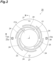
- Fig. 2 is a plan view of the mirror device 20 illustrated in Fig. 1 .
- Fig. 3 is a cross-sectional view of the mirror device 20 along line III-III illustrated in Fig. 2 .
- the mirror device 20 includes a base 22, a frame part 23, and a plurality of elastic support parts 24 in addition to the movable mirror 21.
- the movable mirror 21, the base 22, the frame part 23, and the plurality of elastic support parts 24 are configured by a silicon on insulator (SOI) substrate 200. That is, the mirror device 20 is a micro electro mechanical systems (MEMS) mirror device.
- the SOI substrate 200 includes a support layer 201, a device layer 202, and an intermediate layer 203.
- the support layer 201 and the device layer 202 are semiconductor layers (for example, silicon layers).
- the intermediate layer 203 is an insulating layer (for example, a silicon oxide layer) disposed between the support layer 201 and the device layer 202.
- the base 22 is formed by the support layer 201 and has, for example, a disc shape.
- the base 22 has an opening 22a.
- the opening 22a has, for example, a circular shape centered on a center of the base 22 when viewed from a thickness direction of the base 22.
- a thickness of the base 22 may be, for example, about 320 ⁇ m.
- the frame part 23 is formed by the device layer 202 and has, for example, an annular shape.
- the frame part 23 is disposed on a surface 22b of the base 22 on the intermediate layer 203 side via the intermediate layer 203.
- a thickness of the frame part 23 may be, for example, about 30 ⁇ m.
- a thickness of the intermediate layer 203 may be, for example, about 1.5 ⁇ m.
- the movable mirror 21 is formed by the device layer 202 and has, for example, a disc shape.
- the movable mirror 21 is disposed on an inner side of the frame part 23 and faces the opening 22a in the thickness direction of the base 22.
- a metal film 25 forming the mirror surface 21a is disposed on a surface 21b of the movable mirror 21 on a side opposite to the opening 22a.
- a thickness of the movable mirror 21 may be, for example, about 30 ⁇ m.
- a diameter of the movable mirror 21 may be, for example, about 500 ⁇ m.
- the plurality of elastic support parts 24 are formed by the device layer 202.
- Each of the elastic support parts 24 has, for example, an arc shape centered on the center of the base 22 when viewed from the thickness direction of the base 22.
- Each elastic support part 24 is disposed between the frame part 23 and the movable mirror 21.
- One end of each elastic support part 24 is connected to the frame part 23, and the other end of each elastic support part 24 is connected to the movable mirror 21.
- Each elastic support part 24 faces a peripheral portion 22c of the opening 22a in the base 22 in the thickness direction of the base 22.
- a gap is formed between each elastic support part 24 and the peripheral portion 22c.
- a pair of electrode pads 26 are disposed on the surface 22b of the base 22. Each of the electrode pads 26 is positioned in an opening 23a formed in the frame part 23 and the intermediate layer 203 so that the surface 22b of the base 22 is exposed.
- a pair of electrode pads 27 are disposed on a surface 23b of the frame part 23 on a side opposite to the intermediate layer 203. The pair of electrode pads 26 and the pair of electrode pads 27 are disposed at intervals of 90 degrees centered on the center of the base 22 so that the electrode pads 26 and the electrode pads 27 are alternately aligned when viewed from the thickness direction of the base 22.
- a wire 28 electrically connected to the control unit 60 (see Fig. 1 ) is connected to each of the electrode pads 26 and 27.
- each elastic support part 24 is elastically deformed periodically, and the movable mirror 21 reciprocates in a direction perpendicular to the mirror surface 21a.
- the movable mirror 21 performs a reciprocating operation at a frequency of 1 kHz or more (for example, 100 kHz) by resonating in the mirror device 20.
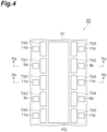
- Fig. 4 is a plan view of the pixel 51 of the optical sensor 50 illustrated in Fig. 1 .
- (a) of Fig. 5 is a cross-sectional view of the pixel 51 along line Va-Va illustrated in Fig. 4
- (b) of Fig. 5 is a cross-sectional view of the pixel 51 along line Vb-Vb illustrated in Fig. 4 .
- the optical sensor 50 includes a semiconductor substrate 1 having a first main surface 1a and a second main surface 1b facing each other.
- the semiconductor substrate 1 includes a p-type first semiconductor region 3 positioned on the first main surface 1a side and a p - -type second semiconductor region 5 having a lower impurity concentration than the first semiconductor region 3 and positioned on the second main surface 1b side.
- the semiconductor substrate 1 can be obtained, for example, by growing a p - -type epitaxial layer having a lower impurity concentration than a p-type semiconductor substrate on the p-type semiconductor substrate.
- An insulating layer 7 is formed on the second main surface 1b (the second semiconductor region 5) of the semiconductor substrate 1.
- a photogate electrode PG is disposed on the insulating layer 7.
- the photogate electrode PG has, for example, a rectangular shape in a plan view.
- a region corresponding to the photogate electrode PG (a region positioned below the photogate electrode PG in Fig. 5 ) in the semiconductor substrate 1 (the second semiconductor region 5) functions as a light receiving part 2 that generates electric charge due to the incident light. That is, the optical sensor 50 includes a plurality of light receiving parts 2 disposed two-dimensionally.
- n-type third semiconductor regions 9a and 9b having a high impurity concentration are formed to face each other in regions positioned away from the photogate electrode PG.
- the third semiconductor region 9a is a first charge accumulation part for accumulating the electric charge generated in the light receiving part 2
- the third semiconductor region 9b is a second charge accumulation part for accumulating the electric charge generated in the light receiving part 2.
- the third semiconductor regions 9a and 9b are disposed to face each other with the photogate electrode PG interposed therebetween.
- the third semiconductor regions 9a and 9b have, for example, a square shape in a plan view.
- n-type third semiconductor regions 9c and 9d having a high impurity concentration are formed to face each other in regions positioned away from the photogate electrode PG.
- the third semiconductor region 9c is a third charge accumulation part for accumulating the electric charge generated in the light receiving part 2
- the third semiconductor region 9d is a fourth charge accumulation part for accumulating the electric charge generated in the light receiving part 2.
- the third semiconductor regions 9c and 9d are disposed to face each other with the photogate electrode PG interposed therebetween.
- the third semiconductor regions 9c and 9d have, for example, a square shape in a plan view.
- the third semiconductor regions 9a and 9c are disposed to face each other with a fourth semiconductor region 11a to be described later interposed therebetween.
- the third semiconductor regions 9b and 9d are disposed to face each other with a fourth semiconductor region 11b to be described later interposed therebetween.
- the n-type fourth semiconductor regions 11a and 11b having a high impurity concentration are formed in regions positioned away from the photogate electrode PG.
- the fourth semiconductor regions 11a and 11b are charge discharge parts for discharging the electric charge generated by the light receiving part 2 to the outside.
- three pairs of the fourth semiconductor regions 11a and 11b are disposed for the photogate electrode PG.
- the fourth semiconductor regions 11a and 11b are disposed to face each other with the photogate electrode PG interposed therebetween.
- the fourth semiconductor regions 11a and 11b have, for example, a square shape in a plan view.
- an impurity concentration is high means that, for example, an impurity concentration is about 1 ⁇ 10 17 cm -3 or higher, and “+” is appended as a conductive type thereof.
- an impurity concentration is low means that, for example, an impurity concentration is about 10 ⁇ 10 15 cm -3 or lower, and "-” is appended as a conductive type thereof.
- a thickness/impurity concentration of each semiconductor region is as follows. A thickness of the first semiconductor region 3: 10 to 1000 ⁇ m/impurity concentration: 1 ⁇ 10 12 cm -3 to 1 ⁇ 10 19 cm -3 .
- a thickness of the second semiconductor region 5 1 to 50 ⁇ m/impurity concentration: 1 ⁇ 10 12 cm -3 to 1 ⁇ 10 15 cm -3 .
- Thicknesses of the third semiconductor regions 9a and 9b and the fourth semiconductor regions 11a and 11b 0.1 to 1 ⁇ m/impurity concentration: 1 ⁇ 10 18 cm -3 to 1 ⁇ 10 20 cm -3 .
- a reference potential such as a ground potential is applied to the semiconductor substrate 1 (the first semiconductor region 3 and the second semiconductor region 5) via a back gate, a through electrode, or the like.
- a transfer electrode TX1, a transfer electrode TX2, a transfer electrode TX3, and a transfer electrode TX4 are disposed on the insulating layer 7 to correspond to the photogate electrode PG.
- the transfer electrode TX1 is positioned between the photogate electrode PG and the third semiconductor region 9a, and is disposed away from the photogate electrode PG.
- the transfer electrode TX2 is positioned between the photogate electrode PG and the third semiconductor region 9b, and is disposed away from the photogate electrode PG.
- the transfer electrode TX3 is positioned between the photogate electrode PG and the third semiconductor region 9c, and is disposed away from the photogate electrode PG.
- the transfer electrode TX4 is positioned between the photogate electrode PG and the third semiconductor region 9d, and is disposed away from the photogate electrode PG.
- the transfer electrodes TX1 to TX4 have, for example, a rectangular shape in a plan view.
- a region of the semiconductor substrate 1 (the second semiconductor region 5) corresponding to the transfer electrode TX1 functions as a transfer gate 4a for transferring electric charge generated in the light receiving part 2 to the third semiconductor region 9a which is the first charge accumulation part.
- a region of the semiconductor substrate 1 (the second semiconductor region 5) corresponding to the transfer electrode TX2 functions as a transfer gate 4b for transferring electric charge generated in the light receiving part 2 to the third semiconductor region 9b which is the second charge accumulation part.
- a region of the semiconductor substrate 1 (the second semiconductor region 5) corresponding to the transfer electrode TX3 functions as a transfer gate 4c for transferring electric charge generated in the light receiving part 2 to the third semiconductor region 9c which is the third charge accumulation part.
- a region of the semiconductor substrate 1 (the second semiconductor region 5) corresponding to the transfer electrode TX4 functions as a transfer gate 4d for transferring electric charge generated in the light receiving part 2 to the third semiconductor region 9d which is the fourth charge accumulation part.
- a plurality (here, six) of transfer electrodes TX5 are disposed on the insulating layer 7 to correspond to the photogate electrode PG. Some of the plurality of transfer electrodes TX5 on one side of the photogate electrode PG are each positioned between the photogate electrode PG and the fourth semiconductor region 11a, and are disposed away from the photogate electrode PG with the transfer electrode TX1 and the transfer electrode TX3 interposed therebetween. The remainder of the plurality of transfer electrodes TX5 on the other side of the photogate electrode PG are each positioned between the photogate electrode PG and the fourth semiconductor region 11b, and are disposed away from the photogate electrode PG with the transfer electrode TX2 and the transfer electrode TX4 interposed therebetween.
- the transfer electrode TX5 has, for example, a rectangular shape in a plan view.
- a region of the semiconductor substrate 1 (the second semiconductor region 5) corresponding to the transfer electrode TX5 on the one side (a region positioned below the transfer electrode TX5 on the one side in Fig. 5 ) functions as a discharge gate 6a for transferring electric charge generated in the light receiving part 2 to the fourth semiconductor region 11a which is the charge discharge part.
- a region of the semiconductor substrate 1 (the second semiconductor region 5) corresponding to the transfer electrode TX5 on the other side functions as a discharge gate 6b for transferring electric charge generated in the light receiving part 2 to the fourth semiconductor region 11b which is the charge discharge part.
- the discharge gates 6a and 6b are for discharging electric charge generated in the light receiving part 2.
- a length dimension of each of the transfer electrodes TX1 to TX5 in a direction facing the photogate electrode PG is determined according to a transferable distance of signal charge and unnecessary charge so that a region of the photogate electrode PG that allows high-speed transfer of the signal charge and the unnecessary charge is covered in each of the transfer electrodes TX1 to TX5.
- a contact hole for exposing a surface of the first semiconductor region 3 is provided in the insulating layer 7.
- a conductor 13 for connecting each of the third semiconductor regions 9a to 9d and each of the fourth semiconductor regions 11a and 11b to the outside are disposed in the contact hole.
- the semiconductor substrate is formed of Si as an example, and the insulating layer 7 is formed of SiO 2 as an example.
- the photogate electrode PG and the transfer electrodes TX1 to TX5 are formed of polysilicon as an example. Further, other materials may be used for those described above.
- the third semiconductor regions 9a to 9d are for accumulating electric charge generated in the light receiving part 2 due to the incident light. Phases of charge transfer signals applied to the transfer electrodes TX1 to TX4 are different from each other. Light incident on one pixel 51 is converted into electric charge in the light receiving part 2, and the electric charge generated in the light receiving part 2 is attracted to the transfer gates 4a to 4d and the discharge gates 6a and 6b side by the photogate electrode PG to which a voltage is applied. The attracted charge travels in directions of the transfer electrodes TX1 to TX4 as signal charge according to a potential energy gradient formed due to the voltages applied to the photogate electrode PG and the transfer electrodes TX1 to TX4.
- An n-type semiconductor contains a positively ionized donor, has a positive potential energy, and attracts electrons.
- an electric potential (ground potential) lower than the above-described positive potential is applied to the transfer electrodes TX1 to TX4, potential energy barriers due to the transfer electrodes TX1 to TX4 are generated, and electric charge generated in the semiconductor substrate 1 is not pulled into the third semiconductor regions 9a to 9d.
- the fourth semiconductor regions 11a and 11b are for collecting unnecessary charge generated in the light receiving part 2 due to the incident light and discharging them to the outside.
- the light incident on one pixel 51 is converted into electric charge in the light receiving part 2, and the electric charge generated in the light receiving part 2 is attracted to the transfer gates 4a to 4d and the discharge gates 6a and 6b side by the photogate electrode PG to which a voltage is applied.
- the attracted charge travels in directions of the transfer electrodes TX5 as unnecessary charge according to a potential energy gradient formed due to the voltages applied to the photogate electrode PG and the transfer electrodes TX5.
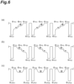
- Fig. 6 is a diagram showing "a potential energy distribution in the vicinity of the second main surface 1b of the semiconductor substrate 1" for explaining an accumulation operation of signal charge.
- Fig. 7 is a diagram showing "a potential energy distribution in the vicinity of the second main surface 1b of the semiconductor substrate 1" for explaining a discharge operation of unnecessary charge.
- a downward direction is a positive direction of a potential energy.
- (a) and (b) show potential energy distributions in a transverse direction of the cross section of Fig. 4 in the transverse direction
- (c) shows a potential energy distribution in a transverse direction of the cross section of Fig. 5 in the transverse direction.
- Fig. 6 is a diagram showing "a potential energy distribution in the vicinity of the second main surface 1b of the semiconductor substrate 1" for explaining an accumulation operation of signal charge.
- Fig. 7 is a diagram showing "a potential energy distribution in the vicinity of the second main surface 1b of the semiconductor substrate 1" for explaining a discharge operation of unnecessary charge.
- a downward direction is
- Figs. 6 and 7 show a potential energy ⁇ TX1 in a region (the transfer gate 4a) just below the transfer electrode TX1, a potential energy ⁇ TX2 in a region (the transfer gate 4b) just below the transfer electrode TX2, a potential energy ⁇ TX5 in a region (the discharge gates 6a and 6b) just below the transfer electrode TX5, a potential energy ⁇ PG of the light receiving part 2 just below the photogate electrode PG, a potential energy ⁇ FD1 of the third semiconductor region 9a, a potential energy ⁇ FD2 of the third semiconductor region 9b, a potential energy ⁇ OFD1 of the fourth semiconductor region 11a, and a potential energy ⁇ OFD2 of the fourth semiconductor region 11b.
- the potential energy ⁇ PG of the light receiving part 2 just below the photogate electrode PG is set higher than the reference potential.
- the potential energy ⁇ PG of the light receiving part 2 is higher than the potential energies ⁇ TX1 , ⁇ TX2 , and ⁇ TX5 and a potential energy distribution in this region has a downwardly concave shape in the drawing.
- the potential energy ⁇ TX2 of the region just below the transfer electrode TX2 is not lowered, and electric charge does not flow into the potential energy well of the third semiconductor region 9b.
- the potential energy ⁇ TX2 of the region just below the transfer electrode TX2 is not lowered, and electric charge does not flow into the potential energy well of the third semiconductor region 9b.
- the potential energy is recessed in a positive direction.
- the signal charge is collected and accumulated in the potential energy wells of the third semiconductor regions 9a and 9b.
- the signal charges accumulated in the potential energy wells of the third semiconductor regions 9a and 9b are read out to the outside.
- the set of the transfer electrode TX1 and the transfer electrode TX2 has been described, and the same applies to the set of the transfer electrode TX3 and the transfer electrode TX4.
- a state in which a predetermined electric potential is applied to the transfer electrodes TX1 to TX4, and the regions just below the transfer electrodes TX1 to TX4, that is, the transfer gates 4a to 4d, can transfer electric charge to the third semiconductor regions 9a to 9d may be referred to as a charge transfer state.
- the transfer gates 4a to 4d being in the charge transfer state may be referred to as the transfer gates 4a to 4d being in an ON state.
- a state in which a predetermined electric potential is applied to the transfer electrodes TX5, and the regions just below the transfer electrodes TX5, that is, the discharge gates 6a and 6b, can transfer electric charge to the fourth semiconductor regions 11a and 11b may be referred to as a charge discharge state.
- the discharge gates 6a and 6b being in the charge discharge state may be referred to as the discharge gates 6a and 6b being in an ON state.
- the optical sensor 50 includes a reset transistor (not illustrated) provided in the pixel 51.
- reset processing is executed.
- the reset voltage is a positive voltage with an electric potential of the photogate electrode PG as a reference. Thereby, the electric charge accumulated in the third semiconductor regions 9a to 9d and the like serving as the charge accumulation part is discharged to the outside, and it becomes a state in which electric charge is not accumulated.
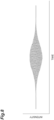
- Fig. 8 is a graph showing an interferogram signal of the interfering light L10 acquired in each pixel 51 of the optical sensor 50 when the movable mirror 21 is moved in any one direction of the doubleheaded arrow over a distance longer than a coherence length of the light L0 in the configuration illustrated in Fig. 1 .
- the envelope curve of the interferogram signal represents a structure of the object S in a depth direction.
- a width of the envelope curve is determined by the coherence length of the light L0 and defines a resolution of the optical coherence tomography device 100 in the depth direction.
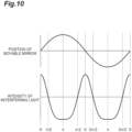
- a part of a time range is cut off accordingly from the interferogram signal shown in Fig. 8 , and the interferogram signal obtained there becomes a signal in a form of reciprocating in terms of time.
- a period of the interferogram signal of the interfering light L10 corresponds to half of a center wavelength (or peak wavelength) of the light L0 emitted from the light source 10.
- control unit 60 applies an electric signal to each pixel 51 of the optical sensor 50 so that the four transfer gates 4a, 4b, 4c, and 4d are sequentially brought into the charge transfer state in four time ranges separated from each other and the plurality of discharge gates 6a and 6b are simultaneously brought into the charge discharge state in a time range other than the four time ranges for each period of the interferogram signal of the interfering light L10.
- Fig. 9 is a timing chart of an electric signal applied to each pixel 51 of the optical sensor 50.
- An electric signal VTX1 is an electric signal applied to the transfer electrode TX1 and is an electric signal that brings the transfer gate 4a into the charge transfer state (ON state) in a time range T1 ( ⁇ t/4) repeated in the period T.
- the electric signal VTX2 is an electric signal applied to the transfer electrode TX2 and is an electric signal that brings the transfer gate 4b into the charge transfer state (ON state) in a time range T2 ( ⁇ t/4) repeated in the period T.
- a phase of the electric signal VTX2 is delayed by T/4 with respect to that of the electric signal VTX1.
- the electric signal VTX3 is an electric signal applied to the transfer electrode TX3 and is an electric signal that brings the transfer gate 4c into the charge transfer state (ON state) in a time range T3 ( ⁇ t/4) repeated in the period T.
- a phase of the electric signal VTX3 is delayed by T/4 with respect to that of the electric signal VTX2.
- the electric signal VTX4 is an electric signal applied to the transfer electrode TX4 and is an electric signal that brings the transfer gate 4d into the charge transfer state (ON state) in a time range T4 ( ⁇ t/4) repeated in the period T.
- a phase of the electric signal VTX4 is delayed by T/4 with respect to that of the electric signal VTX3.
- the electric signal VTX5 is an electric signal applied to the plurality of discharge gates 6a and 6b at the same time and is an electric signal that brings the plurality of discharge gates 6a and 6b into the charge discharge state (ON state) in a time range other than the time ranges T1, T2, T3, and T4 (in other words, a time range T5 repeated in the period T/4). Further, the time ranges T1, T2, T3, and T4 each have the same length. Also, the time ranges T1, T2, T3, and T4 are each smaller than the time range T5.
- the control unit 60 acquires four intensities V0, V1, V2, and V3 of the interfering light L10 in each period T of the interferogram signal of the interfering light L10 by applying the above electric signals VTX1, VTX2, VTX3, VTX4, and VTX5 to each pixel 51 of the optical sensor 50.
- the control unit 60 can reproduce an envelope curve of the interferogram signal of the interfering light L10 for each pixel 51 of the optical sensor 50 with high accuracy and generate an image (tomographic image) of the object S with high accuracy.
- the optical coherence tomography device 100 when the movable mirror 21 is reciprocated, a temporal change of an interferogram signal is made periodic, and conversion of the interferogram signal into an envelope curve is facilitated. Then, in each pixel 51 included in the optical sensor 50, the plurality of transfer gates 4a, 4b, 4c, and 4d are sequentially brought into the charge transfer state in four time ranges separated from each other and the discharge gates 6a and 6b are simultaneously brought into the charge discharge state in a time range other than the four time ranges for each period of the interferogram signal of the interfering light L10. Thereby, only the electric charge generated in the light receiving part 2 can be acquired as a signal charge in each of the four time ranges.
- an envelope curve of the interferogram signal of the interfering light L10 can be acquired with high accuracy.
- the acquisition of the signal charge as described above is particularly effective when a speed of the reciprocating operation of the movable mirror 21 is not constant and the interferogram signal of the interfering light L10 has an asymmetrical shape.
- the movable mirror 21 performs the reciprocating operation by resonating in the mirror device 20. Thereby, the interferogram signal of the interfering light L10 can be acquired at high speed. Also, a speed of the reciprocating operation of the movable mirror 21 does not become constant due to the resonance operation of the movable mirror 21, but even in that case, an envelope curve of the interferogram signal of the interfering light L10 can be acquired with high accuracy as described above.
- the movable mirror 21 performs a reciprocating operation at a frequency of 1 kHz or higher.
- the interferogram signal of the interfering light L10 can be acquired at high speed.
- a speed of the reciprocating operation of the movable mirror 21 does not easily become constant, but even in that case, an envelope curve of the interferogram signal of the interfering light L10 can be acquired with high accuracy as described above.
- the interferogram signal of the interfering light L10 can be converted into an envelope curve thereof by digitizing a two-dimensional image using a normal two-dimensional sensor (high-speed camera, or the like) and then performing image processing.
- a normal two-dimensional sensor high-speed camera, or the like
- the plurality of pixels 51 are disposed two-dimensionally. Thereby, an image of a predetermined region of the object S can be generated at once. Further, in such a case in which the interfering light L10 is detected by a single PD, the interferogram signal of the interfering light L10 can be converted into an envelope curve thereof by performing digital signal processing after AD conversion of waveform data at high speed. However, in such a case in which the interfering light L10 is detected by a plurality of PDs disposed two-dimensionally, it is difficult to process the waveform data at high speed and convert the interferogram signal of the interfering light L10 into an envelope curve thereof.
- the mirror device 20 is a MEMS mirror device. Thereby, the movable mirror 21 can be reciprocated at high speed.
- each pixel 51 includes the photogate electrode PG.
- time ranges T1, T2, T3, and T4 have the same length as each other in the above-described embodiment, but the time ranges T1, T2, T3, and T4 may not have the same length as each other.
- a start timing of the time range T5 in which the discharge gates 6a and 6b are in the charge discharge state has been configured to match an end timing of each of the time ranges T1, T2, T3 and T4 in which each of the transfer gates 4a, 4b, 4c, and 4d is in the charge transfer state, but when the end timing of the time range T5 matches the start timing of each of the time ranges T1, T2, T3, and T4, the start timing of the time range T5 may be delayed from the end timing of each of the time ranges T1, T2, T3, and T4.
- the control unit 60 may apply an electric signal to the optical sensor 50 so that the plurality of transfer gates (at least two of the transfer gates 4a, 4b, 4c, and 4d) are sequentially brought into the charge transfer state in at least three time ranges separated from each other and the discharge gate (at least one of the discharge gates 6a and 6b) is brought into the charge discharge state in a time range other than the at least three time ranges for each period of the interferogram signal of the interfering light L10.
- a center wavelength of the light L0 is set to ⁇ .
- Each of at least three time ranges (for example, four time ranges) in which electric charge is acquired in each period of the interferogram signal of the interfering light L10 may be a time range centered on a time at which a phase of the interferogram signal of the interfering light L10 is shifted by ⁇ /2. According to this, a calculation for converting the interferogram signal of the interfering light L10 into an envelope curve thereof can be simplified. Due to simplification of the calculation, some or all of the calculation can be realized by hardware, and this can contribute to overall high-speed processing.
- the interferogram signal of the interfering light L10 cannot be accurately converted into an envelope curve thereof when, for example a speed of the reciprocating operation of the movable mirror 21 is not constant, or an acquisition of electric charge is not performed at regular time intervals (in the latter case, even if the speed of the reciprocating operation of the movable mirror 21 is constant).
- an envelope curve of the interferogram signal of the interfering light L10 can be acquired with high accuracy.
- each pixel 51 may include two transfer gates 4a and 4b as illustrated in Fig. 14 (two transfer electrodes TX1 and TX2 corresponding to two transfer gates 4a and 4b are illustrated in Fig. 14 ). That is, each pixel 51 may include a plurality of transfer gates. In the optical sensor 50, the plurality of pixels 51 may be disposed one-dimensionally.
- the mirror device 20 may be one in which the movable mirror 21 is reciprocated by a magnetic force, or one in which the movable mirror 21 is reciprocated by a drive source such as a piezo actuator.
- an envelope curve of an interferogram signal of interfering light can be acquired with high accuracy in the optical coherence tomography device including a mirror device whose operation speed of the movable mirror is not constant. At this time, if an amount of movement of the movable mirror is distorted with respect to a control signal, this can be easily compensated by adjusting each time range, that allows each transfer gate of the optical sensor to be in the charge transfer state, in accordance with the distortion of the amount of movement of the movable mirror.
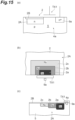
- the light receiving part 2 is not limited to the photogate structure and may have another structure.
- the light receiving part 2 may have an embedded PD structure.
- the light receiving part 2 is configured by a p + -type semiconductor region 2B provided in the second semiconductor region 5 on the second main surface 1b side, and an n-type semiconductor region 2A provided in the second semiconductor region 5 just below the semiconductor region 2B.
- a potential energy gradient can be provided in the light receiving part 2 to perform high-speed charge transfer.
- a configuration in which the n-type semiconductor region 2A includes, for example, a plurality (here, three) of n-type semiconductor regions 2a, 2b, and 2c disposed so that an impurity concentration increases toward the transfer gate 4a, and thereby forming an electric field gradient can be exemplified.
- (b) of Fig. 15 is a schematic cross-sectional view
- (c) of Fig. 15 is a plan view.
- a configuration for providing a potential energy gradient in the light receiving part 2 as illustrated in Fig. 16 , a configuration in which the n-type semiconductor region 2A includes a pair of n-type semiconductor regions 2d and 2e, and an n + -type semiconductor region 2f that is sandwiched between the semiconductor regions 2d and 2e and whose width W extends toward, for example, the transfer gate 4a, and thereby forming an electric field gradient can be exemplified.
- Fig. 16 is a plan view from the second main surface 1b side.
- 100 optical coherence tomography device
- 2 light receiving part
- 4a, 4b, 4c, 4d transfer gate
- 6a, 6b discharge gate
- 10 light source
- 20 mirror device
- 21 movable mirror
- 30 support part
- 40 beam splitter
- 50 optical sensor
- 51 pixel
- PG photogate electrode
- 60 control unit
- L0 light
- L1 first light
- L2 second light
- L10 interfering light
- S object.
Landscapes
- Physics & Mathematics (AREA)
- General Physics & Mathematics (AREA)
- Health & Medical Sciences (AREA)
- General Health & Medical Sciences (AREA)
- Engineering & Computer Science (AREA)
- Signal Processing (AREA)
- Multimedia (AREA)
- Radiology & Medical Imaging (AREA)
- Nuclear Medicine, Radiotherapy & Molecular Imaging (AREA)
- Analytical Chemistry (AREA)
- Pathology (AREA)
- Immunology (AREA)
- Biochemistry (AREA)
- Chemical & Material Sciences (AREA)
- Life Sciences & Earth Sciences (AREA)
- Investigating Or Analysing Materials By Optical Means (AREA)
- Solid State Image Pick-Up Elements (AREA)
Claims (7)
- Optische Kohärenztomographievorrichtung (100), umfassend:eine Lichtquelle (10);eine Spiegelvorrichtung (20) einschließlich eines beweglichen Spiegels, der zum Durchführen einer Hin- und Herbewegung konfiguriert ist;einen Stützteil (30), der zum Stützen eines Objekts konfiguriert ist;einen Strahlteiler (40), der dazu konfiguriert ist, Interferenzlicht zu erzeugen, indem er von der Lichtquelle ausgesandtes Licht in ein erstes Licht und ein zweites Licht aufspaltet und das vom beweglichen Spiegel reflektierte erste Licht und das vom Objekt reflektierte zweite Licht kombiniert;einen optischen Sensor (50), der dazu konfiguriert ist, das vom Strahlteiler erzeugte Interferenzlicht zu erfassen; undeine Steuereinheit (60), die zumindest mit dem optischen Sensor elektrisch verbunden ist, wobeider optische Sensor eine Vielzahl von Pixeln (51) einschließt, wobei jedes der Vielzahl von Pixeln (51)einen Lichtempfangsteil (2) einschließt, der so konfiguriert ist, dass er aufgrund von einfallendem Licht elektrische Ladung erzeugt,eine Vielzahl von Transfergattern (4a, 4b, 4c, 4d), die dazu konfiguriert sind, die im Lichtempfangsteil erzeugte elektrische Ladung zu übertragen, undein Entladetor (6a, 6b), das dazu konfiguriert ist, die im Lichtempfangsteil erzeugte elektrische Ladung zu entladen, unddie Steuereinheit ein elektrisches Signal auf den optischen Sensor anwendet, so dass die Vielzahl von Transfergattern nacheinander in mindestens drei voneinander getrennten Zeitbereichen in einen Ladungstransferzustand gebracht werden und das Entladungstor in einem anderen Zeitbereich als den mindestens drei Zeitbereichen für jede Periode eines Interferogrammsignals des Interferenzlichts in einen Ladungs-Entladungszustand gebracht wird.
- Optische Kohärenztomographievorrichtung nach Anspruch 1, wobei der bewegliche Spiegel so konfiguriert ist, dass er durch Resonanz in der Spiegelvorrichtung eine Hin- und Herbewegung durchführt.
- Optische Kohärenztomographievorrichtung nach Anspruch 1 oder 2, wobei der bewegliche Spiegel dazu konfiguriert ist, eine Hin- und Herbewegung mit einer Frequenz von 1 kHz oder höher durchzuführen.
- Optische Kohärenztomographievorrichtung nach einem der Ansprüche 1 bis 3, wobei die Vielzahl von Pixeln zweidimensional angeordnet ist.
- Optische Kohärenztomographievorrichtung nach einem der Ansprüche 1 bis 4, wobei die Spiegelvorrichtung eine MEMS-Spiegelvorrichtung ist.
- Optische Kohärenztomographievorrichtung nach einem der Ansprüche 1 bis 5, wobei jedes der Vielzahl von Pixeln weiter eine Photogate-Elektrode einschließt, die dazu konfiguriert ist, die im Lichtempfangsteil erzeugte elektrische Ladung zu der Vielzahl von Transfergattern und der Entladungstor-Seite zu ziehen.
- Optische Kohärenztomographievorrichtung nach einem der Ansprüche 1 bis 6, wobei jeder der mindestens drei Zeitbereiche ein Zeitbereich ist, der auf einen Zeitpunkt zentriert ist, zu dem eine Phase des Interferogrammsignals um π/2 verschoben ist.
Applications Claiming Priority (3)
| Application Number | Priority Date | Filing Date | Title |
|---|---|---|---|
| JP2020027369 | 2020-02-20 | ||
| JP2020133011A JP7510815B2 (ja) | 2020-02-20 | 2020-08-05 | 光干渉断層撮影装置 |
| PCT/JP2021/002096 WO2021166544A1 (ja) | 2020-02-20 | 2021-01-21 | 光干渉断層撮影装置 |
Publications (3)
| Publication Number | Publication Date |
|---|---|
| EP4087233A1 EP4087233A1 (de) | 2022-11-09 |
| EP4087233A4 EP4087233A4 (de) | 2024-02-14 |
| EP4087233B1 true EP4087233B1 (de) | 2024-08-07 |
Family
ID=77391973
Family Applications (1)
| Application Number | Title | Priority Date | Filing Date |
|---|---|---|---|
| EP21757783.2A Active EP4087233B1 (de) | 2020-02-20 | 2021-01-21 | Vorrichtung für optische kohärenztomografie |
Country Status (4)
| Country | Link |
|---|---|
| US (1) | US12098920B2 (de) |
| EP (1) | EP4087233B1 (de) |
| CN (1) | CN115088249B (de) |
| WO (1) | WO2021166544A1 (de) |
Family Cites Families (14)
| Publication number | Priority date | Publication date | Assignee | Title |
|---|---|---|---|---|
| EP1458087B1 (de) | 2003-03-10 | 2005-10-12 | CSEM Centre Suisse d'Electronique et de Microtechnique SA | Elektrische Schaltung, Verfahren und Vorrichtung zur Demodulation eines intensitätsmodulierten Signals |
| JP4191001B2 (ja) * | 2003-10-07 | 2008-12-03 | 本田技研工業株式会社 | 4輪駆動車両の動力伝達系性能確認方法 |
| JP3793531B2 (ja) | 2003-10-07 | 2006-07-05 | オリンパス株式会社 | 蛍光寿命測定装置 |
| JP4971891B2 (ja) * | 2007-07-03 | 2012-07-11 | 浜松ホトニクス株式会社 | 裏面入射型測距センサ及び測距装置 |
| EP2924465B1 (de) * | 2007-07-03 | 2017-11-29 | Hamamatsu Photonics K.K. | Rückbeleuchteter entfernungsmessungssensor und entfernungsmessungsvorrichtung |
| JP5623028B2 (ja) * | 2009-01-23 | 2014-11-12 | キヤノン株式会社 | 光干渉断層画像を撮る撮像方法及びその装置 |
| JP2011177379A (ja) * | 2010-03-02 | 2011-09-15 | Panasonic Corp | 光断層画像取得装置 |
| US20130003077A1 (en) * | 2010-03-31 | 2013-01-03 | Canon Kabushiki Kaisha | Tomographic imaging apparatus and control apparatus for tomographic imaging apparatus |
| EP2668465A1 (de) * | 2011-01-25 | 2013-12-04 | Massachusetts Institute Of Technology | Monoshot-vollfeld-reflexionsphasen-mikroskopie |
| JP6231940B2 (ja) | 2014-05-08 | 2017-11-15 | 浜松ホトニクス株式会社 | 測距装置及び測距装置の駆動方法 |
| EP3333893B1 (de) | 2015-08-04 | 2020-02-19 | Panasonic Intellectual Property Management Co., Ltd. | Festkörperbildgebungsvorrichtung |
| CN107370913B (zh) * | 2016-05-11 | 2021-03-16 | 松下知识产权经营株式会社 | 摄像装置、摄像系统以及光检测方法 |
| US11658193B2 (en) | 2018-01-23 | 2023-05-23 | Samsung Electronics Co., Ltd. | Image sensor |
| JP7363782B2 (ja) | 2018-07-02 | 2023-10-18 | Toppanホールディングス株式会社 | 測距装置、カメラ、検査調整装置、測距装置の駆動調整方法及び検査調整方法 |
-
2021
- 2021-01-21 EP EP21757783.2A patent/EP4087233B1/de active Active
- 2021-01-21 WO PCT/JP2021/002096 patent/WO2021166544A1/ja not_active Ceased
- 2021-01-21 US US17/798,377 patent/US12098920B2/en active Active
- 2021-01-21 CN CN202180014608.8A patent/CN115088249B/zh active Active
Also Published As
| Publication number | Publication date |
|---|---|
| EP4087233A1 (de) | 2022-11-09 |
| EP4087233A4 (de) | 2024-02-14 |
| CN115088249B (zh) | 2025-04-25 |
| CN115088249A (zh) | 2022-09-20 |
| WO2021166544A1 (ja) | 2021-08-26 |
| US12098920B2 (en) | 2024-09-24 |
| US20230083427A1 (en) | 2023-03-16 |
Similar Documents
| Publication | Publication Date | Title |
|---|---|---|
| KR101751090B1 (ko) | 거리 화상 센서 | |
| TWI221730B (en) | Light receiving device with controllable sensitivity and spatial information detecting apparatus using the same | |
| US9117712B1 (en) | Demodulation pixel with backside illumination and charge barrier | |
| CN101310387A (zh) | 用于对调制电磁波场进行解调的器件和方法 | |
| US10008621B2 (en) | Controlling of photo-generated charge carriers | |
| EP1611618B1 (de) | Lichtempfänger mit kontrollierter empfindlichkeit und detektionsvorrichtung mit räumlicher auflösung | |
| US20090224139A1 (en) | Drift Field Demodulation Pixel with Pinned Photo Diode | |
| JP6265346B2 (ja) | 距離計測装置 | |
| US9698196B2 (en) | Demodulation pixel incorporating majority carrier current, buried channel and high-low junction | |
| JP7651472B2 (ja) | フォトディテクタ | |
| EP3497470B1 (de) | Demodulator mit einer ladungsträgererzeugenden gepinnten photodiode und verfahren zum betrieb desselben | |
| CN110729315B (zh) | 像素架构和图像传感器 | |
| EP2821812B1 (de) | Bereichssensor und bereichsbildsensor | |
| EP4087233B1 (de) | Vorrichtung für optische kohärenztomografie | |
| US20110167913A1 (en) | Imaging devices for measuring the structure of a surface | |
| JP7510815B2 (ja) | 光干渉断層撮影装置 | |
| JP2006084429A (ja) | 距離画像センサ | |
| WO2012076500A1 (en) | Method and system for demodulating signals | |
| CN115552279A (zh) | 带有偏置衬底的镜组件中的电容感测 | |
| US9053998B2 (en) | Range sensor and range image sensor | |
| EP4040187A1 (de) | Lichtdetektionsvorrichtung und elektronische vorrichtung | |
| JP2007093620A (ja) | 受光素子の感度制御方法、強度変調光を用いた空間情報の検出装置 | |
| Heinz | Optical vibration detection with a four-point photoconductance-monitoring array | |
| JP2012083222A (ja) | 距離センサ及び距離画像センサ |
Legal Events
| Date | Code | Title | Description |
|---|---|---|---|
| STAA | Information on the status of an ep patent application or granted ep patent |
Free format text: STATUS: THE INTERNATIONAL PUBLICATION HAS BEEN MADE |
|
| PUAI | Public reference made under article 153(3) epc to a published international application that has entered the european phase |
Free format text: ORIGINAL CODE: 0009012 |
|
| STAA | Information on the status of an ep patent application or granted ep patent |
Free format text: STATUS: REQUEST FOR EXAMINATION WAS MADE |
|
| 17P | Request for examination filed |
Effective date: 20220804 |
|
| AK | Designated contracting states |
Kind code of ref document: A1 Designated state(s): AL AT BE BG CH CY CZ DE DK EE ES FI FR GB GR HR HU IE IS IT LI LT LU LV MC MK MT NL NO PL PT RO RS SE SI SK SM TR |
|
| DAV | Request for validation of the european patent (deleted) | ||
| DAX | Request for extension of the european patent (deleted) | ||
| REG | Reference to a national code |
Ipc: G01S0007481000 Ref country code: DE Ref legal event code: R079 Ref document number: 602021016926 Country of ref document: DE Free format text: PREVIOUS MAIN CLASS: H04N0005335000 |
|
| A4 | Supplementary search report drawn up and despatched |
Effective date: 20240116 |
|
| RIC1 | Information provided on ipc code assigned before grant |
Ipc: G01B 9/02091 20220101ALI20240110BHEP Ipc: G01N 21/17 20060101ALI20240110BHEP Ipc: G01S 17/89 20200101ALI20240110BHEP Ipc: G01S 7/481 20060101AFI20240110BHEP |
|
| GRAP | Despatch of communication of intention to grant a patent |
Free format text: ORIGINAL CODE: EPIDOSNIGR1 |
|
| STAA | Information on the status of an ep patent application or granted ep patent |
Free format text: STATUS: GRANT OF PATENT IS INTENDED |
|
| RIC1 | Information provided on ipc code assigned before grant |
Ipc: G01B 9/02091 20220101ALI20240322BHEP Ipc: G01N 21/17 20060101ALI20240322BHEP Ipc: G01S 17/89 20200101ALI20240322BHEP Ipc: G01S 7/481 20060101AFI20240322BHEP |
|
| INTG | Intention to grant announced |
Effective date: 20240423 |
|
| GRAS | Grant fee paid |
Free format text: ORIGINAL CODE: EPIDOSNIGR3 |
|
| GRAA | (expected) grant |
Free format text: ORIGINAL CODE: 0009210 |
|
| STAA | Information on the status of an ep patent application or granted ep patent |
Free format text: STATUS: THE PATENT HAS BEEN GRANTED |
|
| AK | Designated contracting states |
Kind code of ref document: B1 Designated state(s): AL AT BE BG CH CY CZ DE DK EE ES FI FR GB GR HR HU IE IS IT LI LT LU LV MC MK MT NL NO PL PT RO RS SE SI SK SM TR |
|
| REG | Reference to a national code |
Ref country code: GB Ref legal event code: FG4D |
|
| REG | Reference to a national code |
Ref country code: CH Ref legal event code: EP |
|
| REG | Reference to a national code |
Ref country code: IE Ref legal event code: FG4D |
|
| REG | Reference to a national code |
Ref country code: DE Ref legal event code: R096 Ref document number: 602021016926 Country of ref document: DE |
|
| P01 | Opt-out of the competence of the unified patent court (upc) registered |
Free format text: CASE NUMBER: APP_52213/2024 Effective date: 20240917 |
|
| REG | Reference to a national code |
Ref country code: LT Ref legal event code: MG9D |
|
| REG | Reference to a national code |
Ref country code: NL Ref legal event code: MP Effective date: 20240807 |
|
| PG25 | Lapsed in a contracting state [announced via postgrant information from national office to epo] |
Ref country code: NO Free format text: LAPSE BECAUSE OF FAILURE TO SUBMIT A TRANSLATION OF THE DESCRIPTION OR TO PAY THE FEE WITHIN THE PRESCRIBED TIME-LIMIT Effective date: 20241107 |
|
| REG | Reference to a national code |
Ref country code: AT Ref legal event code: MK05 Ref document number: 1711540 Country of ref document: AT Kind code of ref document: T Effective date: 20240807 |
|
| PG25 | Lapsed in a contracting state [announced via postgrant information from national office to epo] |
Ref country code: PT Free format text: LAPSE BECAUSE OF FAILURE TO SUBMIT A TRANSLATION OF THE DESCRIPTION OR TO PAY THE FEE WITHIN THE PRESCRIBED TIME-LIMIT Effective date: 20241209 Ref country code: NL Free format text: LAPSE BECAUSE OF FAILURE TO SUBMIT A TRANSLATION OF THE DESCRIPTION OR TO PAY THE FEE WITHIN THE PRESCRIBED TIME-LIMIT Effective date: 20240807 Ref country code: FI Free format text: LAPSE BECAUSE OF FAILURE TO SUBMIT A TRANSLATION OF THE DESCRIPTION OR TO PAY THE FEE WITHIN THE PRESCRIBED TIME-LIMIT Effective date: 20240807 Ref country code: GR Free format text: LAPSE BECAUSE OF FAILURE TO SUBMIT A TRANSLATION OF THE DESCRIPTION OR TO PAY THE FEE WITHIN THE PRESCRIBED TIME-LIMIT Effective date: 20241108 Ref country code: PL Free format text: LAPSE BECAUSE OF FAILURE TO SUBMIT A TRANSLATION OF THE DESCRIPTION OR TO PAY THE FEE WITHIN THE PRESCRIBED TIME-LIMIT Effective date: 20240807 |
|
| PG25 | Lapsed in a contracting state [announced via postgrant information from national office to epo] |
Ref country code: BG Free format text: LAPSE BECAUSE OF FAILURE TO SUBMIT A TRANSLATION OF THE DESCRIPTION OR TO PAY THE FEE WITHIN THE PRESCRIBED TIME-LIMIT Effective date: 20240807 |
|
| PG25 | Lapsed in a contracting state [announced via postgrant information from national office to epo] |
Ref country code: LV Free format text: LAPSE BECAUSE OF FAILURE TO SUBMIT A TRANSLATION OF THE DESCRIPTION OR TO PAY THE FEE WITHIN THE PRESCRIBED TIME-LIMIT Effective date: 20240807 |
|
| PG25 | Lapsed in a contracting state [announced via postgrant information from national office to epo] |
Ref country code: AT Free format text: LAPSE BECAUSE OF FAILURE TO SUBMIT A TRANSLATION OF THE DESCRIPTION OR TO PAY THE FEE WITHIN THE PRESCRIBED TIME-LIMIT Effective date: 20240807 Ref country code: IS Free format text: LAPSE BECAUSE OF FAILURE TO SUBMIT A TRANSLATION OF THE DESCRIPTION OR TO PAY THE FEE WITHIN THE PRESCRIBED TIME-LIMIT Effective date: 20241207 |
|
| PG25 | Lapsed in a contracting state [announced via postgrant information from national office to epo] |
Ref country code: HR Free format text: LAPSE BECAUSE OF FAILURE TO SUBMIT A TRANSLATION OF THE DESCRIPTION OR TO PAY THE FEE WITHIN THE PRESCRIBED TIME-LIMIT Effective date: 20240807 |
|
| PG25 | Lapsed in a contracting state [announced via postgrant information from national office to epo] |
Ref country code: ES Free format text: LAPSE BECAUSE OF FAILURE TO SUBMIT A TRANSLATION OF THE DESCRIPTION OR TO PAY THE FEE WITHIN THE PRESCRIBED TIME-LIMIT Effective date: 20240807 Ref country code: RS Free format text: LAPSE BECAUSE OF FAILURE TO SUBMIT A TRANSLATION OF THE DESCRIPTION OR TO PAY THE FEE WITHIN THE PRESCRIBED TIME-LIMIT Effective date: 20241107 |
|
| PG25 | Lapsed in a contracting state [announced via postgrant information from national office to epo] |
Ref country code: RS Free format text: LAPSE BECAUSE OF FAILURE TO SUBMIT A TRANSLATION OF THE DESCRIPTION OR TO PAY THE FEE WITHIN THE PRESCRIBED TIME-LIMIT Effective date: 20241107 Ref country code: PT Free format text: LAPSE BECAUSE OF FAILURE TO SUBMIT A TRANSLATION OF THE DESCRIPTION OR TO PAY THE FEE WITHIN THE PRESCRIBED TIME-LIMIT Effective date: 20241209 Ref country code: PL Free format text: LAPSE BECAUSE OF FAILURE TO SUBMIT A TRANSLATION OF THE DESCRIPTION OR TO PAY THE FEE WITHIN THE PRESCRIBED TIME-LIMIT Effective date: 20240807 Ref country code: NO Free format text: LAPSE BECAUSE OF FAILURE TO SUBMIT A TRANSLATION OF THE DESCRIPTION OR TO PAY THE FEE WITHIN THE PRESCRIBED TIME-LIMIT Effective date: 20241107 Ref country code: NL Free format text: LAPSE BECAUSE OF FAILURE TO SUBMIT A TRANSLATION OF THE DESCRIPTION OR TO PAY THE FEE WITHIN THE PRESCRIBED TIME-LIMIT Effective date: 20240807 Ref country code: LV Free format text: LAPSE BECAUSE OF FAILURE TO SUBMIT A TRANSLATION OF THE DESCRIPTION OR TO PAY THE FEE WITHIN THE PRESCRIBED TIME-LIMIT Effective date: 20240807 Ref country code: IS Free format text: LAPSE BECAUSE OF FAILURE TO SUBMIT A TRANSLATION OF THE DESCRIPTION OR TO PAY THE FEE WITHIN THE PRESCRIBED TIME-LIMIT Effective date: 20241207 Ref country code: HR Free format text: LAPSE BECAUSE OF FAILURE TO SUBMIT A TRANSLATION OF THE DESCRIPTION OR TO PAY THE FEE WITHIN THE PRESCRIBED TIME-LIMIT Effective date: 20240807 Ref country code: GR Free format text: LAPSE BECAUSE OF FAILURE TO SUBMIT A TRANSLATION OF THE DESCRIPTION OR TO PAY THE FEE WITHIN THE PRESCRIBED TIME-LIMIT Effective date: 20241108 Ref country code: FI Free format text: LAPSE BECAUSE OF FAILURE TO SUBMIT A TRANSLATION OF THE DESCRIPTION OR TO PAY THE FEE WITHIN THE PRESCRIBED TIME-LIMIT Effective date: 20240807 Ref country code: ES Free format text: LAPSE BECAUSE OF FAILURE TO SUBMIT A TRANSLATION OF THE DESCRIPTION OR TO PAY THE FEE WITHIN THE PRESCRIBED TIME-LIMIT Effective date: 20240807 Ref country code: BG Free format text: LAPSE BECAUSE OF FAILURE TO SUBMIT A TRANSLATION OF THE DESCRIPTION OR TO PAY THE FEE WITHIN THE PRESCRIBED TIME-LIMIT Effective date: 20240807 Ref country code: AT Free format text: LAPSE BECAUSE OF FAILURE TO SUBMIT A TRANSLATION OF THE DESCRIPTION OR TO PAY THE FEE WITHIN THE PRESCRIBED TIME-LIMIT Effective date: 20240807 |
|
| PG25 | Lapsed in a contracting state [announced via postgrant information from national office to epo] |
Ref country code: SM Free format text: LAPSE BECAUSE OF FAILURE TO SUBMIT A TRANSLATION OF THE DESCRIPTION OR TO PAY THE FEE WITHIN THE PRESCRIBED TIME-LIMIT Effective date: 20240807 Ref country code: DK Free format text: LAPSE BECAUSE OF FAILURE TO SUBMIT A TRANSLATION OF THE DESCRIPTION OR TO PAY THE FEE WITHIN THE PRESCRIBED TIME-LIMIT Effective date: 20240807 |
|
| PG25 | Lapsed in a contracting state [announced via postgrant information from national office to epo] |
Ref country code: EE Free format text: LAPSE BECAUSE OF FAILURE TO SUBMIT A TRANSLATION OF THE DESCRIPTION OR TO PAY THE FEE WITHIN THE PRESCRIBED TIME-LIMIT Effective date: 20240807 |
|
| PG25 | Lapsed in a contracting state [announced via postgrant information from national office to epo] |
Ref country code: CZ Free format text: LAPSE BECAUSE OF FAILURE TO SUBMIT A TRANSLATION OF THE DESCRIPTION OR TO PAY THE FEE WITHIN THE PRESCRIBED TIME-LIMIT Effective date: 20240807 |
|
| PG25 | Lapsed in a contracting state [announced via postgrant information from national office to epo] |
Ref country code: SK Free format text: LAPSE BECAUSE OF FAILURE TO SUBMIT A TRANSLATION OF THE DESCRIPTION OR TO PAY THE FEE WITHIN THE PRESCRIBED TIME-LIMIT Effective date: 20240807 |
|
| REG | Reference to a national code |
Ref country code: DE Ref legal event code: R097 Ref document number: 602021016926 Country of ref document: DE |
|
| PLBE | No opposition filed within time limit |
Free format text: ORIGINAL CODE: 0009261 |
|
| STAA | Information on the status of an ep patent application or granted ep patent |
Free format text: STATUS: NO OPPOSITION FILED WITHIN TIME LIMIT |
|
| 26N | No opposition filed |
Effective date: 20250508 |
|
| PG25 | Lapsed in a contracting state [announced via postgrant information from national office to epo] |
Ref country code: SE Free format text: LAPSE BECAUSE OF FAILURE TO SUBMIT A TRANSLATION OF THE DESCRIPTION OR TO PAY THE FEE WITHIN THE PRESCRIBED TIME-LIMIT Effective date: 20240807 |
|
| PG25 | Lapsed in a contracting state [announced via postgrant information from national office to epo] |
Ref country code: MC Free format text: LAPSE BECAUSE OF FAILURE TO SUBMIT A TRANSLATION OF THE DESCRIPTION OR TO PAY THE FEE WITHIN THE PRESCRIBED TIME-LIMIT Effective date: 20240807 Ref country code: LU Free format text: LAPSE BECAUSE OF NON-PAYMENT OF DUE FEES Effective date: 20250121 |
|
| GBPC | Gb: european patent ceased through non-payment of renewal fee |
Effective date: 20250121 |
|
| PG25 | Lapsed in a contracting state [announced via postgrant information from national office to epo] |
Ref country code: GB Free format text: LAPSE BECAUSE OF NON-PAYMENT OF DUE FEES Effective date: 20250121 Ref country code: BE Free format text: LAPSE BECAUSE OF NON-PAYMENT OF DUE FEES Effective date: 20250131 |
|
| REG | Reference to a national code |
Ref country code: BE Ref legal event code: MM Effective date: 20250131 |
|
| PGFP | Annual fee paid to national office [announced via postgrant information from national office to epo] |
Ref country code: FR Payment date: 20251128 Year of fee payment: 6 |
|
| PG25 | Lapsed in a contracting state [announced via postgrant information from national office to epo] |
Ref country code: IE Free format text: LAPSE BECAUSE OF NON-PAYMENT OF DUE FEES Effective date: 20250121 |
|
| PG25 | Lapsed in a contracting state [announced via postgrant information from national office to epo] |
Ref country code: IT Free format text: LAPSE BECAUSE OF FAILURE TO SUBMIT A TRANSLATION OF THE DESCRIPTION OR TO PAY THE FEE WITHIN THE PRESCRIBED TIME-LIMIT Effective date: 20240807 |
|
| REG | Reference to a national code |
Ref country code: CH Ref legal event code: U11 Free format text: ST27 STATUS EVENT CODE: U-0-0-U10-U11 (AS PROVIDED BY THE NATIONAL OFFICE) Effective date: 20260201 |
|
| PGFP | Annual fee paid to national office [announced via postgrant information from national office to epo] |
Ref country code: DE Payment date: 20251203 Year of fee payment: 6 |
|
| PG25 | Lapsed in a contracting state [announced via postgrant information from national office to epo] |
Ref country code: RO Free format text: LAPSE BECAUSE OF FAILURE TO SUBMIT A TRANSLATION OF THE DESCRIPTION OR TO PAY THE FEE WITHIN THE PRESCRIBED TIME-LIMIT Effective date: 20240807 |
|
| PGFP | Annual fee paid to national office [announced via postgrant information from national office to epo] |
Ref country code: CH Payment date: 20260201 Year of fee payment: 6 |