EP4082176B1 - Elektronische vorrichtung mit antennenmodul - Google Patents
Elektronische vorrichtung mit antennenmodul Download PDFInfo
- Publication number
- EP4082176B1 EP4082176B1 EP20918071.0A EP20918071A EP4082176B1 EP 4082176 B1 EP4082176 B1 EP 4082176B1 EP 20918071 A EP20918071 A EP 20918071A EP 4082176 B1 EP4082176 B1 EP 4082176B1
- Authority
- EP
- European Patent Office
- Prior art keywords
- antenna
- electronic device
- connection member
- bridge
- support member
- Prior art date
- Legal status (The legal status is an assumption and is not a legal conclusion. Google has not performed a legal analysis and makes no representation as to the accuracy of the status listed.)
- Active
Links
Images


Classifications
-
- H—ELECTRICITY
- H04—ELECTRIC COMMUNICATION TECHNIQUE
- H04M—TELEPHONIC COMMUNICATION
- H04M1/00—Substation equipment, e.g. for use by subscribers
- H04M1/02—Constructional features of telephone sets
- H04M1/0202—Portable telephone sets, e.g. cordless phones, mobile phones or bar type handsets
- H04M1/026—Details of the structure or mounting of specific components
-
- H—ELECTRICITY
- H04—ELECTRIC COMMUNICATION TECHNIQUE
- H04M—TELEPHONIC COMMUNICATION
- H04M1/00—Substation equipment, e.g. for use by subscribers
- H04M1/02—Constructional features of telephone sets
- H04M1/0202—Portable telephone sets, e.g. cordless phones, mobile phones or bar type handsets
- H04M1/0249—Details of the mechanical connection between the housing parts or relating to the method of assembly
-
- H—ELECTRICITY
- H01—ELECTRIC ELEMENTS
- H01Q—ANTENNAS, i.e. RADIO AERIALS
- H01Q1/00—Details of, or arrangements associated with, antennas
- H01Q1/12—Supports; Mounting means
- H01Q1/22—Supports; Mounting means by structural association with other equipment or articles
- H01Q1/24—Supports; Mounting means by structural association with other equipment or articles with receiving set
- H01Q1/241—Supports; Mounting means by structural association with other equipment or articles with receiving set used in mobile communications, e.g. GSM
- H01Q1/242—Supports; Mounting means by structural association with other equipment or articles with receiving set used in mobile communications, e.g. GSM specially adapted for hand-held use
- H01Q1/243—Supports; Mounting means by structural association with other equipment or articles with receiving set used in mobile communications, e.g. GSM specially adapted for hand-held use with built-in antennas
-
- H—ELECTRICITY
- H01—ELECTRIC ELEMENTS
- H01Q—ANTENNAS, i.e. RADIO AERIALS
- H01Q1/00—Details of, or arrangements associated with, antennas
- H01Q1/36—Structural form of radiating elements, e.g. cone, spiral, umbrella; Particular materials used therewith
- H01Q1/38—Structural form of radiating elements, e.g. cone, spiral, umbrella; Particular materials used therewith formed by a conductive layer on an insulating support
-
- H—ELECTRICITY
- H01—ELECTRIC ELEMENTS
- H01Q—ANTENNAS, i.e. RADIO AERIALS
- H01Q1/00—Details of, or arrangements associated with, antennas
- H01Q1/42—Housings not intimately mechanically associated with radiating elements, e.g. radome
-
- H—ELECTRICITY
- H04—ELECTRIC COMMUNICATION TECHNIQUE
- H04M—TELEPHONIC COMMUNICATION
- H04M1/00—Substation equipment, e.g. for use by subscribers
- H04M1/02—Constructional features of telephone sets
- H04M1/0202—Portable telephone sets, e.g. cordless phones, mobile phones or bar type handsets
- H04M1/026—Details of the structure or mounting of specific components
- H04M1/0277—Details of the structure or mounting of specific components for a printed circuit board assembly
-
- H—ELECTRICITY
- H05—ELECTRIC TECHNIQUES NOT OTHERWISE PROVIDED FOR
- H05K—PRINTED CIRCUITS; CASINGS OR CONSTRUCTIONAL DETAILS OF ELECTRIC APPARATUS; MANUFACTURE OF ASSEMBLAGES OF ELECTRICAL COMPONENTS
- H05K5/00—Casings, cabinets or drawers for electric apparatus
- H05K5/0017—Casings, cabinets or drawers for electric apparatus with operator interface units
-
- H—ELECTRICITY
- H05—ELECTRIC TECHNIQUES NOT OTHERWISE PROVIDED FOR
- H05K—PRINTED CIRCUITS; CASINGS OR CONSTRUCTIONAL DETAILS OF ELECTRIC APPARATUS; MANUFACTURE OF ASSEMBLAGES OF ELECTRICAL COMPONENTS
- H05K7/00—Constructional details common to different types of electric apparatus
- H05K7/14—Mounting supporting structure in casing or on frame or rack
- H05K7/1422—Printed circuit boards receptacles, e.g. stacked structures, electronic circuit modules or box like frames
- H05K7/1427—Housings
-
- H—ELECTRICITY
- H04—ELECTRIC COMMUNICATION TECHNIQUE
- H04B—TRANSMISSION
- H04B1/00—Details of transmission systems, not covered by a single one of groups H04B3/00 - H04B13/00; Details of transmission systems not characterised by the medium used for transmission
- H04B1/38—Transceivers, i.e. devices in which transmitter and receiver form a structural unit and in which at least one part is used for functions of transmitting and receiving
- H04B1/3827—Portable transceivers
Definitions
- Various embodiments of the disclosure relate to an electronic device including an antenna module.
- An electronic device may transmit and receive various data to and from another electronic device through wireless communication.
- Such an electronic device may include at least one antenna to perform long-distance communication and short-range communication.
- US 2017/0244151 A1 discusses an example of an electronic device capable of improved efficiency of a plurality of antennas included in the electronic device.
- US 2018/278731 A1 discloses a so-called coupled feeding antenna that connects a metal housing and a feeder with a capacitive element.
- US 2017/047641 A1 aims to provide an antenna device and an electronic device including the antenna device which is capable of contributing to the improvement of a sensing function and the optimization of a leakage current, as well as contributing to the improvement of an antenna radiation performance.
- US 2019/067821 A1 provides an antenna device and/or an electronic device with such antenna devices that are utilized to secure a resonance frequency in multiple different frequency bands even in a small space.
- At least some of the housing constituting the external appearance of an electronic device may be made of a conductive material (e.g., metal).
- the electronic device may use at least a portion of the housing as a radiator of an antenna for wireless communication.
- the housing may be segmented by a cut-off portion into multiple parts, which may be used as plural antennas.
- the plural antennas may cover various frequency bands.
- an electronic device includes: a housing constituting an external appearance of the electronic device; a support member including a first bridge; a printed circuit board coupled to one surface of the support member; a first antenna constituting a first part of the housing and connected to the support member through the first bridge; a second antenna constituting a second part of the housing; a cut-off portion separating the first antenna and the second antenna; and a first connection member and a second connection member coupled to the first bridge, wherein the first connection member may be connected to a ground of the printed circuit board through a first capacitor and may be disposed closer to the cut-off portion than the second connection member connected to the ground of the printed circuit board through a second capacitor.
- various functions described below can be implemented or supported by one or more computer programs, each of which is formed from computer readable program code and embodied in a computer readable medium.
- application and “program” refer to one or more computer programs, software components, sets of instructions, procedures, functions, objects, classes, instances, related data, or a portion thereof adapted for implementation in a suitable computer readable program code.
- computer readable program code includes any type of computer code, including source code, object code, and executable code.
- computer readable medium includes any type of medium capable of being accessed by a computer, such as read only memory(ROM), random access memory(RAM), a hard disk drive, a compact disc(CD), a digital video disc(DVD), or any other type of memory.
- ROM read only memory
- RAM random access memory
- CD compact disc
- DVD digital video disc
- a "non-transitory” computer readable medium excludes wired, wireless, optical, or other communication links that transport transitory electrical or other signals.
- a non-transitory computer readable medium includes media where data can be permanently stored and media where data can be stored and later overwritten, such as a rewritable optical disc or an erasable memory device.
- FIGS. 1 through 14 discussed below, and the various embodiments used to describe the principles of the present disclosure in this patent document are by way of illustration only and should not be construed in any way to limit the scope of the disclosure. Those skilled in the art will understand that the principles of the present disclosure may be implemented in any suitably arranged system or device.
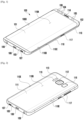
- FIG. 1 illustrates a perspective view of the front surface of a mobile electronic device according to an embodiment of the disclosure.
- FIG. 2 illustrates a perspective view of the rear surface of the electronic device of FIG. 1 according to an embodiment of the disclosure.
- an electronic device 100 may include a housing 110 including a first surface (or front surface) 110A, a second surface (or rear surface) 110B, and a side surface 110C surrounding the space between the first surface 110A and the second surface 110B.
- the housing may denote a structure that forms a part of the first surface 110A, the second surface 110B, and the side surface 110C illustrated in FIG. 1 .
- the first surface 110A may be formed by a front plate 102, at least a part of which is substantially transparent (for example, a glass plate including various coating layers, or a polymer plate).
- the second surface 110B may be formed by a rear plate 111 that is substantially opaque.
- the rear plate 111 may be made of coated or colored glass, ceramic, polymer, metal (for example, aluminum, stainless steel (STS), or magnesium), or a combination of at least two of the above-mentioned materials.
- the side surface 110C may be formed by a side bezel structure (or "side member") 118 which is coupled to the front plate 102 and to the rear plate 111, and which includes metal and/or polymer.
- the rear plate 111 and the side bezel structure 118 may be formed integrally and may include the same material (for example, a metal material such as aluminum).
- the front plate 102 may include two first areas 110D on both ends of the long edge of the front plate 102 such that the two first areas 110D bend from the first surface 110A toward the rear plate 111 and extend seamlessly.
- the rear plate 111 may include two second areas 110E on both ends of the long edge such that the two second areas 110E bend from the second surface 110B toward the front plate 102 and extend seamlessly.
- the front plate 102 (or the rear plate 111) may include only one of the first areas 110D (or the second areas 110E). In another embodiment, a part of the first areas 110D or the second areas 110E may not be included.
- the side bezel structure 118 when seen from the side surface of the electronic device 100, may have a first thickness (or width) on a part of the side surface, which does not include the first areas 110D or the second areas 110E as described above, and may have a second thickness that is smaller than the first thickness on a part of the side surface, which includes the first areas 110D or the second areas 110E.
- the electronic device 100 may include at least one of a display 101, audio modules 103, 107, and 114, sensor modules 104, 116, and 119, camera modules 105, 112, and 113, a key input device 117, a light-emitting element 106, and connector holes 108 and 109.
- at least one of the constituent elements for example, the key input device 117 or the light-emitting element 106) of the electronic device 100 may be omitted, or the electronic device 100 may additionally include another constituent element.
- the display 101 may be exposed through a corresponding part of the front plate 102, for example. In some embodiments, at least a part of the display 101 may be exposed through the front plate 102 that forms the first areas 110D of the side surface 110C and the first surface 110A. In some embodiments, the display 101 may have a corner formed in substantially the same shape as that of the adjacent outer periphery of the front plate 102. In another embodiment (not illustrated), in order to increase the area of exposure of the display 101, the interval between the outer periphery of the display 101 and the outer periphery of the front plate 102 may be formed to be substantially identical.
- a recess or an opening may be formed in a part of the screen display area of the display 101, and at least one of an audio module 114, a sensor module 104, a camera module 105, and a light-emitting element 106 may be included and aligned with the recess or the opening.
- at least one of an audio module 114, a sensor module 104, a camera module 105, a fingerprint sensor 116, and a light-emitting element 106 may be included.
- the display 101 may be coupled to or arranged adjacent to a touch sensing circuit, a pressure sensor capable of measuring the intensity (pressure) of a touch, and/or a digitizer that detects a magnetic field-type stylus pen.
- a touch sensing circuit capable of measuring the intensity (pressure) of a touch
- a digitizer capable of measuring the intensity (pressure) of a touch
- a digitizer that detects a magnetic field-type stylus pen.
- at least a part of the sensor modules 104 and 119 and/or at least a part of the key input device 117 may be arranged in the first areas 110D and/or the second areas 110E.
- the audio modules 103, 107, and 114 may include a microphone hole 103 and speaker holes 107 and 114.
- a microphone for acquiring an external sound may be arranged in the microphone hole 103, and a plurality of microphones may be arranged therein such that the direction of a sound can be sensed in some embodiments.
- the speaker holes 107 and 114 may include an outer speaker hole 107 and a speech receiver hole 114.
- the speaker holes 107 and 114 and the microphone hole 103 may be implemented as a single hole, or a speaker may be included (for example, a piezoelectric speaker) without the speaker holes 107 and 114.
- the sensor modules 104, 116, and 119 may generate an electric signal or a data value corresponding to the internal operating condition of the electronic device 100 or the external environment condition thereof.
- the sensor modules 104, 116, and 119 may include, for example, a first sensor module 104 (for example, a proximity sensor) arranged on the first surface 110A of the housing 110, and/or a second sensor module (not illustrated) (for example, a fingerprint sensor), and/or a third sensor module 119 (for example, an HRM sensor) arranged on the second surface 110B of the housing 110, and/or a fourth sensor module 116 (for example, a fingerprint sensor).
- the fingerprint sensor may be arranged not only on the first surface 110A (for example, the display 101) of the housing 110, but also on the second surface 110B thereof.
- the electronic device 100 may further include a sensor module not illustrated, for example, at least one of a gesture sensor, a gyro sensor, an atmospheric pressure sensor, a magnetic sensor, an acceleration sensor, a grip sensor, a color sensor, an infrared (IR) sensor, a biometric sensor, a temperature sensor, a humidity sensor, or a luminance sensor 104.
- a sensor module not illustrated, for example, at least one of a gesture sensor, a gyro sensor, an atmospheric pressure sensor, a magnetic sensor, an acceleration sensor, a grip sensor, a color sensor, an infrared (IR) sensor, a biometric sensor, a temperature sensor, a humidity sensor, or a luminance sensor 104.
- the camera modules 105, 112, and 113 may include a first camera device 105 arranged on the first surface 110A of the electronic device 100, a second camera device 112 arranged on the second surface 110B thereof, and/or a flash 113.
- the camera devices 105 and 112 may include a single lens or a plurality of lenses, an image sensor, and/or an image signal processor.
- the flash 113 may include, for example, a light-emitting diode or a xenon lamp.
- two or more lenses (an infrared camera, a wide-angle lens, and a telephoto lens) and image sensors may be arranged on a single surface of the electronic device 100.
- the key input device 117 may be arranged on the side surface 110C of the housing 110.
- the electronic device 100 may not include a part of the above-mentioned key input device 117 or the entire key input device 117, and the key input device 117 (not included) may be implemented in another type, such as a soft key, on the display 101.
- the key input device may include a sensor module 116 arranged on the second surface 110B of the housing 110.
- the light-emitting element 106 may be arranged on the first surface 110A of the housing 110, for example.
- the light-emitting element 106 may provide information regarding the condition of the electronic device 100 in a light type, for example.
- the light-emitting element 106 may provide a light source that interworks with operation of the camera module 105, for example.
- the light-emitting element 106 may include, for example, a light-emitting diode (LED), an infrared light-emitting diode (IR LED), and a xenon lamp.
- the connector holes 108 and 109 may include a first connector hole 108 capable of containing a connector (for example, a universal serial bus (USB) connector) for transmitting/receiving power and/or data to/from an external electronic device, and/or a second connector hole (for example, an earphone jack) 109 capable of containing a connector for transmitting/receiving an audio signal to/from the external electronic device.
- a connector for example, a universal serial bus (USB) connector
- USB universal serial bus
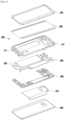
- FIG. 3 is a developed perspective view of an electronic device of FIG. 1 according to an embodiment of the disclosure.
- an electronic device 300 may include a side bezel structure 310, a first support member 311 (for example, a bracket), a front plate 320, a display 330, a printed circuit board 340, a battery 350, a second support member 360 (for example, a rear case), an antenna 370, and a rear plate 380.
- a first support member 311 for example, a bracket
- a front plate 320 for example, a bracket
- a display 330 for example, a display 330
- a printed circuit board 340 for example, a rear case
- an antenna 370 for example, and a rear plate 380.
- at least one of the constituent elements (for example, the first support member 311 or the second support member 360) of the electronic device 300 may be omitted, or the electronic device 300 may further include another constituent element.
- At least one of the constituent elements of the electronic device 300 may be identical or similar to at least one of the constituent elements of the electronic device 100 of FIG. 1 or FIG. 2 , and repeated
- the first support member 311 may be arranged inside the electronic device 300 and connected to the side bezel structure 310, or may be formed integrally with the side bezel structure 310.
- the first support member 311 may be made of a metal material and/or a nonmetal (for example, polymer) material, for example.
- the display 330 may be coupled to one surface of the first support member 311, and the printed circuit board 340 may be coupled to the other surface thereof.
- a processor, a memory, and/or an interface may be mounted on the printed circuit board 340.
- the processor may include, for example, one or more of a central processing device, an application processor, a graphic processing device, an image signal processor, a sensor hub processor, or a communication processor.
- the memory may include a volatile memory or a non-volatile memory, for example.
- the battery 350 is a device for supplying power to at least one constituent element of the electronic device 300, and may include a non-rechargeable primary cell, a rechargeable secondary cell, or a fuel cell, for example. At least a part of the battery 350 may be arranged on substantially the same plane with the printed circuit board 340, for example.
- the battery 350 may be arranged integrally inside the electronic device 300, or may be arranged such that the same can be attached to/detached from the electronic device 300.
- the antenna 370 may be arranged between the rear plate 380 and the battery 350.
- the antenna 370 may include, for example, a near field communication (NFC) antenna, a wireless charging antenna, and/or a magnetic secure transmission (MST) antenna.
- the antenna 370 may conduct near-field communication with an external device or may wirelessly transmit/receive power necessary for charging, for example.
- an antenna structure may be formed by a part or a combination of the side bezel structure 310 and/or the first support member 311.
- a or B at least one of A or/and B
- one or more of A or/and B as used herein include all possible combinations of items enumerated with them.
- “A or B,” “at least one of A and B,” or “at least one of A or B” means (1) including at least one A, (2) including at least one B, or (3) including both at least one A and at least one B.
- first and second may modify various elements regardless of an order and/or importance of the corresponding elements, and do not limit the corresponding elements. These terms may be used for the purpose of distinguishing one element from another element.
- a first user device and a second user device may indicate different user devices regardless of the order or importance.
- a first element may be referred to as a second element without departing from the scope the disclosure, and similarly, a second element may be referred to as a first element.
- module as used herein may be defined as, for example, a unit including one of hardware, software, and firmware or two or more combinations thereof.
- module may be interchangeably used with, for example, the terms “unit”, “logic”, “logical block”, “component”, or “circuit”, and the like.
- the “module” may be a minimum unit of an integrated component or a part thereof.
- the “module” may be a minimum unit performing one or more functions or a part thereof.
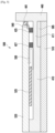
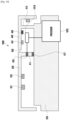
- FIG. 4 illustrates a partial schematic view showing a configuration of an electronic device including an antenna module, according to various embodiments of the disclosure.
- the electronic device 400 of FIG. 4 may include the electronic device 100 or 300 shown in FIGS. 1 to 3 .
- FIG. 4 may be a transparent perspective view of an upper portion of the electronic device 400 when the electronic device 400 is placed vertically.
- the electronic device 400 includes a support member 410, a first antenna 420, a first connection member 425, a second connection member 427, a cut-off portion 430, and a second antenna 440.
- the support member 410 may be disposed inside the electronic device 400.
- the support member 410 may be connected to the first antenna 420 through a first bridge 411.
- the support member 410 may be integrally formed with the first antenna 420 and the second antenna 440 by using the first bridge 411 and the second bridge 413.
- the support member 410 may include the first support member 311 shown in FIG. 3 .
- the support member 410 may be made of, for example, a metal material and/or a non-metal material (e.g., polymer).
- the support member 410 may include a first surface coupled with the display (e.g., display 330 in FIG. 3 ), and a second surface coupled with the printed circuit board (e.g., printed circuit board 340 in FIG. 3 ).
- the first bridge 411 and the second bridge 413 may include a conductive member.
- the first antenna 420 is connected to the support member 410 through the first bridge 411.
- the first antenna 420 may include a first ground part 421 and a first feeding part 423.
- the first ground part 421 and the first feeding part 423 may be disposed on the inner side of the first antenna 420.
- the first ground part 421 may ground the first antenna 420.
- the first feeding part 423 may transmit and receive signals through the first antenna 420.
- the first antenna 420 may be used to transmit and receive signals in a first frequency band (e.g., low or mid frequencies).
- a first frequency band e.g., low or mid frequencies.
- the first antenna 420 may transmit and receive signals of about 600 to 2200 MHz.
- the first frequency band is an example, and signals of other frequency bands may be transmitted and received, according to various embodiments in accordance with this disclosure.
- the first antenna 420 is not limited to the first frequency band, and may be used to transmit and receive signals in a second frequency band (e.g., mid or high frequencies).
- the first feeding part 423 may be disposed closer to the first bridge 411 or the cut-off portion 430 rather than the first ground part 421.
- the positions of the first ground part 421 and the first feeding part 423 may be changed.
- the first ground part 421 may be omitted.
- the first connection member 425 may be formed on a part (e.g., upper part) of the first bridge 411 and may be disposed close to the cut-off portion 430.
- the first connection member 425 may be connected to a first capacitor (e.g., variable capacitor).
- the first capacitor connected to the first connection member 425 may have a variable capacitance value.
- the first connection member 425 may serve as a ground of the first antenna 420.
- the first connection member 425 may be connected to the printed circuit board (e.g., printed circuit board 340 in FIG. 3 ) through a contact component (e.g., C clip).
- the first connection member 425 is connected to the ground of the printed circuit board through the first capacitor.
- the second connection member 427 may be formed on another part (e.g., lower part) of the first bridge 411.
- the second connection member 427 may be disposed under the first connection member 425.
- the second connection member 427 may be formed on the first bridge 411 at a position farther from the cut-off portion 430 than the first connection member 425.
- the second connection member 427 may be connected to a second capacitor (e.g., fixed capacitor).
- the second capacitor connected to the second connection member 427 may have a fixed capacitance value.
- the second connection member 427 may be connected to a contact component (e.g., C clip) provided on the printed circuit board (e.g., printed circuit board 340 in FIG. 3 ).
- the second connection member 427 is connected to the ground of the printed circuit board through the second capacitor.
- the second connection member 427 may serve as a noise stopper that blocks noise generated from electronic components and/or elements mounted on the printed circuit board (e.g., printed circuit board 340 in FIG. 3 ) from being transmitted to the first antenna 420 or the second antenna 440.
- first connection member 425 and the second connection member 427 may be disposed close to the cut-off portion 430 to form a parasitic antenna.
- the cut-off portion 430 may be formed between the first antenna 420 and the second antenna 440.
- the cut-off portion 430 may physically separate the first antenna 420 and the second antenna 440.
- the cut-off portion 430 may be filled with a non-conductive material.
- the non-conductive material may be an insulator (or, dielectric) including at least one of polyimide, plastic, polymer, or ceramic.
- the cut-off portion 430 may prevent foreign substances from entering the electronic device 400 from the outside.
- the second antenna 440 may be connected to the support member 410 through the second bridge 413.
- the second antenna 440 may include a second feeding part 441 and a second ground part 443.
- the second feeding part 441 and the second ground part 443 may be disposed on the inner side of the second antenna 440.
- the second feeding part 441 may transmit and receive signals through the second antenna 440.
- the second ground part 443 may ground the second antenna 440.
- the second feeding part 441 may be disposed closer to the cut-off portion 430 than the second ground part 443.
- the second ground part 443 may be omitted.
- the second antenna 440 may be used to transmit and receive signals in a second frequency band (e.g., mid or high frequencies).
- a second frequency band e.g., mid or high frequencies.
- the second antenna 440 may transmit and receive signals of about 1.2 to 2.2 GHz or about 2.4 to 5.0 GHz.
- the second frequency band is an example, and signals of other frequency bands may be transmitted and received, according to various embodiments in accordance with this disclosure.
- the frequency bands of the first antenna 420 and the second antenna 440 may be different.
- the second antenna 440 is not limited to the second frequency band (e.g., mid or high frequencies) and may be used to transmit and receive signals in the above-described first frequency band (e.g., low or mid frequencies).
- At least a portion of the first antenna 420, the cut-off portion 430, at least a portion of the second antenna 440, the second feeding part 441, and the first connection member 425 and second connection member 427 formed in the first bridge 411 may form a coupling zone 450.
- the first antenna 420, the first ground part 421, the first feeding part 423, the first connection member 425, the second connection member 427, the cut-off portion 430, the second antenna 440, the second feeding part 441 and/or the second ground part 443 may constitute an antenna module.
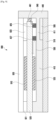
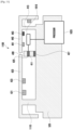
- the electronic device 500 of FIG. 5 may include the electronic device 100, 300 or 400 shown in FIGS. 1 to 4 .
- the embodiment in relation to the electronic device 500 of FIG. 5 may be applied to the embodiment in relation to the electronic device 400 of FIG. 4 described above.
- the electronic device 500 may include a display 510 and a printed circuit board 520.
- the display 510 may be coupled to a first surface of the support member 410.
- the display 510 may be coupled to at least a portion of the support member 410 including the first bridge 411 or second bridge 413 by using an elastic member 505 (e.g., sponge).
- the elastic member 505 may absorb an external shock to prevent damage to the display 510.
- the display 510 may include the display 330 shown in FIG. 3 .
- the display 510 may display information input by the user on the electronic device 500 or display information to be provided to the user.
- the display 510 may perform an input function and a display function.
- the printed circuit board 520 may be coupled to a second surface of the support member 410.
- Various electronic elements 525 may be mounted on the printed circuit board 520.
- the electronic elements 525 mounted on the printed circuit board 520 may include at least one of a processor, a memory, a radio frequency IC (RFIC), a power management IC (PMIC), a charger IC, a modem IC, or an interface.
- the printed circuit board 520 may include contact components (e.g., C-clip, boss hole, screw or rib, conductive pillow foam) for contacting the support member 410, the first connection member 425 and/or the second connection member 427.
- the processor may perform overall operations and process data of the electronic device 500.
- the processor may include at least one of a central processing unit (CPU), an application processor, a graphics processing unit (GPU), an image signal processor, a sensor hub processor, or a communication processor.
- CPU central processing unit
- GPU graphics processing unit
- image signal processor a sensor hub processor
- communication processor a communication processor
- the memory stores programs for processing and controlling the processor equipped in the electronic device 500, an operating system (OS), various applications, and input/output data, and may store a program that controls the overall operation of the electronic device 500.
- the memory may store a user interface provided by the electronic device 500 and various configuration information required for processing in the electronic device 500.
- first connection member 425 and the second connection member 427 may be disposed between the printed circuit board 520 and the support member 410.
- the first connection member 425 may form a path 540 for inducing a current of the second antenna 440 between the second feeding part 441 close to the cut-off portion 430 and the support member 410 (or, first bridge 411).
- the first connection member 425 may be a C clip mounted on the printed circuit board 520 and may be grounded through a capacitor mounted on the printed circuit board 520, forming the path 540.
- the second connection member 427 may be disposed closer to the electronic elements 525 than the first connection member 425.
- the second connection member 427 may block noise generated from the electronic elements 525 mounted on the printed circuit board 520 from being transmitted to the second antenna 440 (or, first antenna 420).
- the second connection member 427 may serve as a trap for preventing noise generated from the electronic elements 525 from being transmitted to the second antenna 440 (or, first antenna 420).
- the second connection member 427 may be a C clip mounted on the printed circuit board 520 and may be grounded through a capacitor mounted on the printed circuit board 520, serving as a noise trap.
- the second connection member 427 may form a noise return path 530 so that noise generated from the electronic elements 525 is not transmitted to the second antenna 440 (or, first antenna 420), and may serve to extend the electrical length of the antenna.
- a portion of the first bridge 411 between the first connection member 425 and the second connection member 427 may operate as a part of the antenna.
- FIGS. 6 to 8 illustrate an operating principle based on the capacitance value of the first connection member in the electronic device including an antenna module according to various embodiments of the disclosure.
- the electronic device 500 of FIGS. 6 to 8 may include the electronic device 100, 300, 400 or 500 shown in FIGS. 1 to 5 .
- the embodiment in relation to the electronic device 500 of FIGS. 6 to 8 may be applied to the embodiment in relation to the electronic device 400 or 500 of FIGS. 4 and 5 described above.
- the resonant length of the second antenna 440 may be varied in the electronic device 500.
- the capacitance value of the first connection member 425 may be variable.
- the capacitance value of the second connection member 427 may be fixed.
- the second connection member 427 may be disposed closer to the electronic elements 525 than the first connection member 425.
- the second connection member 427 may serve to prevent noise generated from the electronic elements 525 from being transmitted to the second antenna 440 (or, first antenna 420). Noise generated from the electronic elements 525 mounted on the printed circuit board 520 may be returned to the printed circuit board 520 through, for example, a C clip being the second connection member 427.
- the second connection member 427 may be a C clip mounted on the printed circuit board 520 and may be grounded through a second capacitor mounted on the printed circuit board 520, serving as a noise trap.
- the electronic device 500 may adjust the electrical length of the antenna by varying the capacitance value of the first connection member 425.
- the resonant length of the second antenna 440 may extend through the cut-off portion 430 and the first connection member 425 to the second connection member 427.
- the resonant length of the second antenna 440 may be shortened to the cut-off portion 430 and the first connection member 425.
- the cut-off portion 430 may form a coupling path between the second antenna 440 and the first connection member 425.
- the second ground part 443 shown in FIGS. 6 to 8 may be connected or opened for efficiency of the second antenna 440.
- the performance of the second antenna 440 may be improved in a band of mid or high frequencies.
- the performance of the second antenna 440 may be improved in a band of low or mid frequencies.
- first connection member 425 and the second connection member 427 may serve as a reinforcement part that reinforces the mechanical strength of the electronic device 500.
- FIG. 9 illustrates a principle in which the first connection member and the second connection member serve as a reinforcement part in the electronic device including an antenna module according to various embodiments of the disclosure.
- the electronic device 900 of FIG. 9 may include the electronic device 100, 300, 400 or 500 shown in FIGS. 1 to 8 .
- the embodiment in relation to the electronic device 900 of FIG. 9 may be applied to the embodiment in relation to the electronic device 400 or 500 of FIGS. 4 to 8 described above.
- the electronic device 900 may include electronic components 910 and a second support member 920 (e.g., rear case).
- a second support member 920 e.g., rear case
- the electronic components 910 may be mounted on one surface of the printed circuit board 520.
- the second support member 920 may cover one surface (e.g., rear surface) of the electronic device 900.
- the second support member 920 may be coupled to at least a portion of the printed circuit board 520 by using at least one rib 921 and 923.
- the second support member 920 may include the second support member 360 shown in FIG. 3 .
- the printed circuit board 520 when pressure such as an impact is applied from the outside of the electronic device 900, the printed circuit board 520 may be bent or damaged.
- the first connection member 425 and the second connection member 427 disposed between the printed circuit board 520 and the support member 410 may serve as a reinforcement part that prevents the printed circuit board 520 from being bent or damaged due to an external impact.
- FIGS. 10 to 13 illustrate an example of tuning the capacitance value of the first connection member in the electronic device including an antenna module according to various embodiments of the disclosure.
- the electronic device 1000, 1100, 1200 or 1300 of FIGS. 10 to 13 may include the electronic device 100, 300, 400, 500 or 900 shown in FIGS. 1 to 9 .
- the embodiment in relation to the electronic device 1000, 1100, 1200 or 1300 of FIGS. 10 to 13 may be applied to the embodiment of FIGS. 4 to 9 described above.
- the electronic device 1000, 1100, 1200 or 1300 may include a switch circuit 1010 and a processor 1020.
- the capacitance value of the first connection member 425 may be variable.
- the capacitance value of the second connection member 427 may be fixed.
- the first connection member 425 may be connected to the switch circuit 1010 configured on the printed circuit board 520.
- the processor 1020 may adjust the capacitance value of the first connection member 425 by switching the switch circuit 1010 on and off.
- the processor 1020 may adjust the capacitance value of the first connection member 425 so that the first antenna 420 or the second antenna 440 may have an optimum resonance value for each frequency band.
- the switch circuit 1010 may be selectively connected to the first connection member 425 through a plurality of shunt capacitors (not shown) having different capacitance values (e.g., first capacitor, second capacitor, ..., n th capacitor) to tune the frequencies of the first antenna 420 and/or the second antenna 440.
- the shunt capacitors may be grounded.
- the processor 1020 may control the switch circuit 1010 to tune the capacitance value of the first connection member 425 to be large or small, thereby optimizing the performance of the first antenna 420 and/or the second antenna 440 for each frequency band.
- the processor 1020 may improve performance of the frequency band corresponding to the specific channel while tuning the capacitance value of the first connection member 425 in units of about 1 pF.
- the first bridge 411 may be separated from the first antenna 420 without being connected thereto.
- the support member 410 and the first antenna 420 may be connected by using a third bridge 1110.
- the electronic device 1200 may further include an additional cut-off portion 1210 in the side housing.
- the first bridge 411 may be formed close to the additional cut-off portion 1210.
- a third feeding part 1211 and a fourth feeding part 1213 may be disposed at positions close to the first bridge 411 and the additional cut-off portion 1210.
- the first connection member 425 may be disposed closer to the additional cut-off portion 1210 than the second connection member 427.
- the first bridge 411 may be separated from the side housing without being connected thereto.
- a bridge may be not formed at a position close to the cut-off portion 430 formed between the first antenna 420 and the second antenna 440.
- FIG. 14 illustrates measurement results for radiation efficiency of the electronic device including an antenna module according to various embodiments of the disclosure.
- the capacitance value of the first connection member 425 is adjusted in a range of about 4.5 to 4.9pF and the capacitance value of the second connection member 427 is about 100pF, it can be seen that the performance (radiation efficiency) of the second antenna 440 in a band of about 2300 to 2800MHz or in a band of about 5000 to 5800MHz is improved by about 2dB from G1 to G2 irrespective of the XGND logic of the first antenna 420.
- At least one embodiment illustrates that the performance of the first antenna 420 is not affected even if the capacitance value of the first connection member 425 is adjusted. In addition, radiation efficiency for each resonance frequency of the second antenna 440 is improved according to the adjustment of the capacitance value of the first connection member 425.
Landscapes
- Engineering & Computer Science (AREA)
- Computer Networks & Wireless Communication (AREA)
- Signal Processing (AREA)
- Microelectronics & Electronic Packaging (AREA)
- Support Of Aerials (AREA)
- Telephone Set Structure (AREA)
Claims (15)
- Elektronische Vorrichtung (100, 300, 400, 500, 900, 1000, 1100, 1200, 1300), die Folgendes umfasst:ein Gehäuse (110), das ein äußeres Erscheinungsbild der elektronischen Vorrichtung bildet;ein Stützelement (311; 410), das eine erste Brücke (411) enthält;eine Leiterplatte (340; 520), die mit einer Oberfläche des Stützelements gekoppelt ist;eine erste Antenne (420), die einen ersten Teil des Gehäuses bildet und über die erste Brücke mit dem Stützelement verbunden ist;eine zweite Antenne (440), die einen zweiten Teil des Gehäuses bildet;einen abgeschnittenen Teil (430), der die erste Antenne und die zweite Antenne trennt; undgekennzeichnet dadurch, dass:ein erstes Verbindungselement (425) und ein zweites Verbindungselement (427) mit der ersten Brücke gekoppelt sind,wobei das erste Verbindungselement über einen ersten Kondensator mit einer Masse der Leiterplatte verbunden ist und näher an dem abgeschnittenen Teil als das zweite Verbindungselement angeordnet ist, das über einen zweiten Kondensator mit der Masse der Leiterplatte verbunden ist.
- Elektronische Vorrichtung nach Anspruch 1, wobei der erste Kondensator ein variabler Kondensator ist.
- Elektronische Vorrichtung nach Anspruch 1, wobei das erste Verbindungselement und das zweite Verbindungselement unter Verwendung einer Kontaktkomponente mit der Leiterplatte verbunden sind.
- Elektronische Vorrichtung nach Anspruch 1, wobei:das Stützelement ferner eine zweite Brücke (413) enthält; unddie zweite Antenne über die zweite Brücke mit dem Stützelement verbunden ist.
- Elektronische Vorrichtung nach Anspruch 1, wobei:die erste Antenne einen ersten Masseteil (421) und einen ersten Speiseteil (423) enthält, die an einer Innenseite ausgebildet sind; unddie zweite Antenne einen zweiten Masseteil und einen zweiten Speiseteil (441) enthält, die an einer Innenseite ausgebildet sind.
- Elektronische Vorrichtung nach Anspruch 5, wobei:der erste Speiseteil näher an dem abgeschnittenen Teil als der erste Masseteil angeordnet ist; undder zweite Speiseteil näher an dem abgeschnittenen Teil als der zweite Masseteil angeordnet ist.
- Elektronische Vorrichtung nach Anspruch 5, wobei mindestens ein Teil der ersten Antenne, der abgeschnittene Teil, mindestens ein Teil der zweiten Antenne, der zweite Speiseteil, das erste Verbindungselement und das zweite Verbindungselement so konfiguriert sind, dass sie eine Kopplungszone (450) bilden.
- Elektronische Vorrichtung nach Anspruch 5, wobei das erste Verbindungselement so konfiguriert ist, dass es einen Pfad (540) zum Induzieren eines Stroms der zweiten Antenne zwischen dem zweiten Speiseteil und der ersten Brücke bildet.
- Elektronische Vorrichtung nach Anspruch 1, wobei das zweite Verbindungselement näher an den auf der Leiterplatte montierten elektronischen Elementen (525) als das erste Verbindungselement angeordnet ist und so konfiguriert ist, dass es verhindert, dass von den elektronischen Elementen erzeugtes Rauschen an die erste Antenne oder die zweite Antenne übertragen wird.
- Elektronische Vorrichtung nach Anspruch 1, wobei sich, wenn das erste Verbindungselement einen niedrigen Kapazitätswert hat, eine Resonanzlänge der zweiten Antenne durch den abgeschnittenen Teil und das erste Verbindungselement zu dem zweiten Verbindungselement erstreckt.
- Elektronische Vorrichtung nach Anspruch 1, wobei, wenn das erste Verbindungselement einen hohen Kapazitätswert hat, eine Resonanzlänge der zweiten Antenne zu dem ersten Verbindungselement verkürzt wird.
- Elektronische Vorrichtung nach Anspruch 1, wobei der abgeschnittene Teil so ausgebildet ist, dass er einen Kopplungspfad zwischen der ersten Antenne und der zweiten Antenne bildet.
- Elektronische Vorrichtung nach Anspruch 1, wobei das erste Verbindungselement und das zweite Verbindungselement zwischen dem Stützelement und der Leiterplatte angeordnet sind.
- Elektronische Vorrichtung nach Anspruch 1, die ferner Folgendes umfasst:einen Schaltkreis (1010); undeinen Prozessor (1020),wobei der Prozessor so konfiguriert ist, dass er einen Kapazitätswert des ersten Verbindungselements durch Steuern des mit dem ersten Verbindungselement verbundenen Schaltkreises anpasst.
- Elektronische Vorrichtung, die Folgendes umfasst:ein Gehäuse, das das äußere Erscheinungsbild der elektronischen Vorrichtung bildet;ein Stützelement, das eine erste Brücke und eine zweite Brücke enthält;eine Leiterplatte, die mit einer Oberfläche des Stützelements gekoppelt ist;ein Display, das mit der anderen Seite des Stützelements gekoppelt ist;eine erste Antenne, die einen ersten Teil des Gehäuses bildet und über die erste Brücke mit dem Stützelement verbunden ist;eine zweite Antenne, die einen zweiten Teil des Gehäuses bildet und über die zweite Brücke mit dem Stützelement verbunden ist;einen abgeschnittenen Teil, der die erste Antenne und die zweite Antenne trennt;gekennzeichnet dadurch, dass:ein erstes Verbindungselement und ein zweites Verbindungselement mit der ersten Brücke gekoppelt sind;ein Schaltkreis mit dem ersten Verbindungselement verbunden ist; undein Prozessor mit dem Display und dem Schaltkreis operativ verbunden ist,wobei der Prozessor so konfiguriert ist, dass er einen Kapazitätswert des ersten Verbindungselements durch Steuern des Schaltkreises anpasst.
Applications Claiming Priority (2)
| Application Number | Priority Date | Filing Date | Title |
|---|---|---|---|
| KR1020200014327A KR102717779B1 (ko) | 2020-02-06 | 2020-02-06 | 안테나 모듈을 포함하는 전자 장치 |
| PCT/KR2020/017911 WO2021157834A1 (en) | 2020-02-06 | 2020-12-09 | Electronic device including antenna module |
Publications (3)
| Publication Number | Publication Date |
|---|---|
| EP4082176A1 EP4082176A1 (de) | 2022-11-02 |
| EP4082176A4 EP4082176A4 (de) | 2023-06-28 |
| EP4082176B1 true EP4082176B1 (de) | 2025-07-02 |
Family
ID=77177910
Family Applications (1)
| Application Number | Title | Priority Date | Filing Date |
|---|---|---|---|
| EP20918071.0A Active EP4082176B1 (de) | 2020-02-06 | 2020-12-09 | Elektronische vorrichtung mit antennenmodul |
Country Status (4)
| Country | Link |
|---|---|
| US (1) | US11594806B2 (de) |
| EP (1) | EP4082176B1 (de) |
| KR (1) | KR102717779B1 (de) |
| WO (1) | WO2021157834A1 (de) |
Families Citing this family (2)
| Publication number | Priority date | Publication date | Assignee | Title |
|---|---|---|---|---|
| WO2023101922A1 (en) * | 2021-12-01 | 2023-06-08 | Lumileds Llc | Combined led and sensor arrangement |
| KR20240081912A (ko) * | 2022-12-01 | 2024-06-10 | 삼성전자주식회사 | 테두리가 복수의 세그먼트로 형성된 하우징을 구비한 전자기기 및 상기 하우징의 제조방법 |
Family Cites Families (12)
| Publication number | Priority date | Publication date | Assignee | Title |
|---|---|---|---|---|
| KR0123221B1 (ko) * | 1994-11-22 | 1997-11-22 | 석진철 | 전력공급시스템의 쇼트 방지장치 |
| US6831607B2 (en) | 2003-01-28 | 2004-12-14 | Centurion Wireless Technologies, Inc. | Single-feed, multi-band, virtual two-antenna assembly having the radiating element of one planar inverted-F antenna (PIFA) contained within the radiating element of another PIFA |
| US8614646B2 (en) * | 2008-03-14 | 2013-12-24 | Qualcomm Incorporated | Adaptive tunable antennas for wireless devices |
| KR101973645B1 (ko) * | 2012-11-13 | 2019-04-29 | 엘지전자 주식회사 | 이동 단말기 |
| WO2016028066A1 (en) | 2014-08-18 | 2016-02-25 | Samsung Electronics Co., Ltd. | Antenna of electronic device |
| US10056695B2 (en) | 2015-07-28 | 2018-08-21 | Apple Inc. | Electronic device antenna with switchable return paths |
| KR102408870B1 (ko) | 2015-08-13 | 2022-06-15 | 삼성전자주식회사 | 안테나 장치 및 그것을 포함하는 전자 장치 |
| KR102306080B1 (ko) | 2015-08-13 | 2021-09-30 | 삼성전자주식회사 | 안테나 장치 및 안테나 장치를 포함하는 전자 장치 |
| KR102433402B1 (ko) | 2016-02-19 | 2022-08-17 | 삼성전자주식회사 | 안테나 및 이를 포함하는 전자 장치 |
| KR102461035B1 (ko) * | 2016-02-20 | 2022-11-01 | 삼성전자주식회사 | 안테나를 포함하는 전자 장치 |
| KR102408139B1 (ko) | 2017-08-25 | 2022-06-15 | 삼성전자주식회사 | 안테나 장치 및 그를 포함하는 전자 장치 |
| CN108832272B (zh) * | 2018-05-29 | 2020-08-21 | 北京小米移动软件有限公司 | 电子设备及其天线结构 |
-
2020
- 2020-02-06 KR KR1020200014327A patent/KR102717779B1/ko active Active
- 2020-12-09 WO PCT/KR2020/017911 patent/WO2021157834A1/en not_active Ceased
- 2020-12-09 EP EP20918071.0A patent/EP4082176B1/de active Active
-
2021
- 2021-01-21 US US17/154,811 patent/US11594806B2/en active Active
Also Published As
| Publication number | Publication date |
|---|---|
| EP4082176A1 (de) | 2022-11-02 |
| KR102717779B1 (ko) | 2024-10-16 |
| US11594806B2 (en) | 2023-02-28 |
| US20210249759A1 (en) | 2021-08-12 |
| EP4082176A4 (de) | 2023-06-28 |
| WO2021157834A1 (en) | 2021-08-12 |
| KR20210100398A (ko) | 2021-08-17 |
Similar Documents
| Publication | Publication Date | Title |
|---|---|---|
| US12100884B2 (en) | Antenna having single non-conductive portion and electronic device including the same | |
| US10477675B1 (en) | Electronic device including capacitive structure | |
| US11246229B2 (en) | Electronic component arrangement structure and electronic device including same | |
| US12034224B2 (en) | Electronic device comprising antenna | |
| KR102613216B1 (ko) | 안테나 및 그것을 포함하는 전자 장치 | |
| US10833403B2 (en) | Antenna and electronic device including same | |
| US12451907B2 (en) | Antenna and electronic device having same | |
| US11984642B2 (en) | Electronic apparatus including antenna connection member | |
| KR102790819B1 (ko) | 기생 주파수 제거 구조를 포함하는 전자 장치 | |
| KR102759982B1 (ko) | 안테나를 포함하는 전자 장치 | |
| US20250174885A1 (en) | Antenna structure and electronic device with same | |
| EP4082176B1 (de) | Elektronische vorrichtung mit antennenmodul | |
| KR102551487B1 (ko) | 안테나 모듈에 대응되도록 배치되는 도전성 구조체 및 그것을 포함하는 전자 장치 | |
| KR102756064B1 (ko) | 안테나 및 그립 센서를 포함하는 전자 장치 | |
| US11563280B2 (en) | Electronic device including antenna | |
| KR102408872B1 (ko) | 공진 주파수를 조정하는 회로 및 이를 포함하는 전자 장치 | |
| KR102937372B1 (ko) | 가변 매칭 회로를 포함하는 전자 장치 | |
| EP4426074A1 (de) | Elektronische vorrichtung mit erdungsstruktur für flexible leiterplatte | |
| KR20250165167A (ko) | 도전성 라인을 포함하는 전자 장치 | |
| KR20250166695A (ko) | 볼륨 키를 포함하는 전자 장치 | |
| KR20250043203A (ko) | 안테나를 포함하는 전자 장치 |
Legal Events
| Date | Code | Title | Description |
|---|---|---|---|
| STAA | Information on the status of an ep patent application or granted ep patent |
Free format text: STATUS: THE INTERNATIONAL PUBLICATION HAS BEEN MADE |
|
| PUAI | Public reference made under article 153(3) epc to a published international application that has entered the european phase |
Free format text: ORIGINAL CODE: 0009012 |
|
| STAA | Information on the status of an ep patent application or granted ep patent |
Free format text: STATUS: REQUEST FOR EXAMINATION WAS MADE |
|
| 17P | Request for examination filed |
Effective date: 20220728 |
|
| AK | Designated contracting states |
Kind code of ref document: A1 Designated state(s): AL AT BE BG CH CY CZ DE DK EE ES FI FR GB GR HR HU IE IS IT LI LT LU LV MC MK MT NL NO PL PT RO RS SE SI SK SM TR |
|
| DAV | Request for validation of the european patent (deleted) | ||
| DAX | Request for extension of the european patent (deleted) | ||
| A4 | Supplementary search report drawn up and despatched |
Effective date: 20230601 |
|
| RIC1 | Information provided on ipc code assigned before grant |
Ipc: H01Q 1/24 20060101ALI20230525BHEP Ipc: H01Q 1/38 20060101ALI20230525BHEP Ipc: H04M 1/02 20060101AFI20230525BHEP |
|
| GRAP | Despatch of communication of intention to grant a patent |
Free format text: ORIGINAL CODE: EPIDOSNIGR1 |
|
| STAA | Information on the status of an ep patent application or granted ep patent |
Free format text: STATUS: GRANT OF PATENT IS INTENDED |
|
| INTG | Intention to grant announced |
Effective date: 20250217 |
|
| GRAS | Grant fee paid |
Free format text: ORIGINAL CODE: EPIDOSNIGR3 |
|
| GRAA | (expected) grant |
Free format text: ORIGINAL CODE: 0009210 |
|
| STAA | Information on the status of an ep patent application or granted ep patent |
Free format text: STATUS: THE PATENT HAS BEEN GRANTED |
|
| AK | Designated contracting states |
Kind code of ref document: B1 Designated state(s): AL AT BE BG CH CY CZ DE DK EE ES FI FR GB GR HR HU IE IS IT LI LT LU LV MC MK MT NL NO PL PT RO RS SE SI SK SM TR |
|
| REG | Reference to a national code |
Ref country code: GB Ref legal event code: FG4D |
|
| REG | Reference to a national code |
Ref country code: CH Ref legal event code: EP |
|
| REG | Reference to a national code |
Ref country code: DE Ref legal event code: R096 Ref document number: 602020054021 Country of ref document: DE |
|
| REG | Reference to a national code |
Ref country code: IE Ref legal event code: FG4D |
|
| REG | Reference to a national code |
Ref country code: NL Ref legal event code: MP Effective date: 20250702 |
|
| PG25 | Lapsed in a contracting state [announced via postgrant information from national office to epo] |
Ref country code: PT Free format text: LAPSE BECAUSE OF FAILURE TO SUBMIT A TRANSLATION OF THE DESCRIPTION OR TO PAY THE FEE WITHIN THE PRESCRIBED TIME-LIMIT Effective date: 20251103 |
|
| PG25 | Lapsed in a contracting state [announced via postgrant information from national office to epo] |
Ref country code: NL Free format text: LAPSE BECAUSE OF FAILURE TO SUBMIT A TRANSLATION OF THE DESCRIPTION OR TO PAY THE FEE WITHIN THE PRESCRIBED TIME-LIMIT Effective date: 20250702 |
|
| REG | Reference to a national code |
Ref country code: AT Ref legal event code: MK05 Ref document number: 1810608 Country of ref document: AT Kind code of ref document: T Effective date: 20250702 |
|
| PG25 | Lapsed in a contracting state [announced via postgrant information from national office to epo] |
Ref country code: IS Free format text: LAPSE BECAUSE OF FAILURE TO SUBMIT A TRANSLATION OF THE DESCRIPTION OR TO PAY THE FEE WITHIN THE PRESCRIBED TIME-LIMIT Effective date: 20251102 |
|
| PGFP | Annual fee paid to national office [announced via postgrant information from national office to epo] |
Ref country code: DE Payment date: 20251120 Year of fee payment: 6 |
|
| PG25 | Lapsed in a contracting state [announced via postgrant information from national office to epo] |
Ref country code: NO Free format text: LAPSE BECAUSE OF FAILURE TO SUBMIT A TRANSLATION OF THE DESCRIPTION OR TO PAY THE FEE WITHIN THE PRESCRIBED TIME-LIMIT Effective date: 20251002 |
|
| REG | Reference to a national code |
Ref country code: LT Ref legal event code: MG9D |
|
| PG25 | Lapsed in a contracting state [announced via postgrant information from national office to epo] |
Ref country code: AT Free format text: LAPSE BECAUSE OF FAILURE TO SUBMIT A TRANSLATION OF THE DESCRIPTION OR TO PAY THE FEE WITHIN THE PRESCRIBED TIME-LIMIT Effective date: 20250702 |
|
| PG25 | Lapsed in a contracting state [announced via postgrant information from national office to epo] |
Ref country code: FI Free format text: LAPSE BECAUSE OF FAILURE TO SUBMIT A TRANSLATION OF THE DESCRIPTION OR TO PAY THE FEE WITHIN THE PRESCRIBED TIME-LIMIT Effective date: 20250702 |
|
| PG25 | Lapsed in a contracting state [announced via postgrant information from national office to epo] |
Ref country code: HR Free format text: LAPSE BECAUSE OF FAILURE TO SUBMIT A TRANSLATION OF THE DESCRIPTION OR TO PAY THE FEE WITHIN THE PRESCRIBED TIME-LIMIT Effective date: 20250702 |
|
| PG25 | Lapsed in a contracting state [announced via postgrant information from national office to epo] |
Ref country code: GR Free format text: LAPSE BECAUSE OF FAILURE TO SUBMIT A TRANSLATION OF THE DESCRIPTION OR TO PAY THE FEE WITHIN THE PRESCRIBED TIME-LIMIT Effective date: 20251003 |
|
| PG25 | Lapsed in a contracting state [announced via postgrant information from national office to epo] |
Ref country code: SE Free format text: LAPSE BECAUSE OF FAILURE TO SUBMIT A TRANSLATION OF THE DESCRIPTION OR TO PAY THE FEE WITHIN THE PRESCRIBED TIME-LIMIT Effective date: 20250702 Ref country code: CZ Free format text: LAPSE BECAUSE OF FAILURE TO SUBMIT A TRANSLATION OF THE DESCRIPTION OR TO PAY THE FEE WITHIN THE PRESCRIBED TIME-LIMIT Effective date: 20250702 |
|
| PG25 | Lapsed in a contracting state [announced via postgrant information from national office to epo] |
Ref country code: LV Free format text: LAPSE BECAUSE OF FAILURE TO SUBMIT A TRANSLATION OF THE DESCRIPTION OR TO PAY THE FEE WITHIN THE PRESCRIBED TIME-LIMIT Effective date: 20250702 |
|
| PG25 | Lapsed in a contracting state [announced via postgrant information from national office to epo] |
Ref country code: PL Free format text: LAPSE BECAUSE OF FAILURE TO SUBMIT A TRANSLATION OF THE DESCRIPTION OR TO PAY THE FEE WITHIN THE PRESCRIBED TIME-LIMIT Effective date: 20250702 Ref country code: BG Free format text: LAPSE BECAUSE OF FAILURE TO SUBMIT A TRANSLATION OF THE DESCRIPTION OR TO PAY THE FEE WITHIN THE PRESCRIBED TIME-LIMIT Effective date: 20250702 |
|
| PG25 | Lapsed in a contracting state [announced via postgrant information from national office to epo] |
Ref country code: RS Free format text: LAPSE BECAUSE OF FAILURE TO SUBMIT A TRANSLATION OF THE DESCRIPTION OR TO PAY THE FEE WITHIN THE PRESCRIBED TIME-LIMIT Effective date: 20251002 |
|
| PG25 | Lapsed in a contracting state [announced via postgrant information from national office to epo] |
Ref country code: ES Free format text: LAPSE BECAUSE OF FAILURE TO SUBMIT A TRANSLATION OF THE DESCRIPTION OR TO PAY THE FEE WITHIN THE PRESCRIBED TIME-LIMIT Effective date: 20250702 |
|
| PG25 | Lapsed in a contracting state [announced via postgrant information from national office to epo] |
Ref country code: RO Free format text: LAPSE BECAUSE OF FAILURE TO SUBMIT A TRANSLATION OF THE DESCRIPTION OR TO PAY THE FEE WITHIN THE PRESCRIBED TIME-LIMIT Effective date: 20250702 |
|
| PG25 | Lapsed in a contracting state [announced via postgrant information from national office to epo] |
Ref country code: SM Free format text: LAPSE BECAUSE OF FAILURE TO SUBMIT A TRANSLATION OF THE DESCRIPTION OR TO PAY THE FEE WITHIN THE PRESCRIBED TIME-LIMIT Effective date: 20250702 |
|
| PG25 | Lapsed in a contracting state [announced via postgrant information from national office to epo] |
Ref country code: DK Free format text: LAPSE BECAUSE OF FAILURE TO SUBMIT A TRANSLATION OF THE DESCRIPTION OR TO PAY THE FEE WITHIN THE PRESCRIBED TIME-LIMIT Effective date: 20250702 |
|
| PG25 | Lapsed in a contracting state [announced via postgrant information from national office to epo] |
Ref country code: IT Free format text: LAPSE BECAUSE OF FAILURE TO SUBMIT A TRANSLATION OF THE DESCRIPTION OR TO PAY THE FEE WITHIN THE PRESCRIBED TIME-LIMIT Effective date: 20250702 |