EP4080587B1 - Solarzelle und elektronische vorrichtung - Google Patents
Solarzelle und elektronische vorrichtung Download PDFInfo
- Publication number
- EP4080587B1 EP4080587B1 EP22169114.0A EP22169114A EP4080587B1 EP 4080587 B1 EP4080587 B1 EP 4080587B1 EP 22169114 A EP22169114 A EP 22169114A EP 4080587 B1 EP4080587 B1 EP 4080587B1
- Authority
- EP
- European Patent Office
- Prior art keywords
- layer
- conductive
- transparent
- region
- solar cell
- Prior art date
- Legal status (The legal status is an assumption and is not a legal conclusion. Google has not performed a legal analysis and makes no representation as to the accuracy of the status listed.)
- Active
Links
Images


Classifications
-
- H—ELECTRICITY
- H10—SEMICONDUCTOR DEVICES; ELECTRIC SOLID-STATE DEVICES NOT OTHERWISE PROVIDED FOR
- H10F—INORGANIC SEMICONDUCTOR DEVICES SENSITIVE TO INFRARED RADIATION, LIGHT, ELECTROMAGNETIC RADIATION OF SHORTER WAVELENGTH OR CORPUSCULAR RADIATION
- H10F77/00—Constructional details of devices covered by this subclass
- H10F77/20—Electrodes
- H10F77/206—Electrodes for devices having potential barriers
- H10F77/211—Electrodes for devices having potential barriers for photovoltaic cells
-
- G—PHYSICS
- G02—OPTICS
- G02B—OPTICAL ELEMENTS, SYSTEMS OR APPARATUS
- G02B27/00—Optical systems or apparatus not provided for by any of the groups G02B1/00 - G02B26/00, G02B30/00
- G02B27/01—Head-up displays
- G02B27/017—Head mounted
-
- G—PHYSICS
- G02—OPTICS
- G02C—SPECTACLES; SUNGLASSES OR GOGGLES INSOFAR AS THEY HAVE THE SAME FEATURES AS SPECTACLES; CONTACT LENSES
- G02C11/00—Non-optical adjuncts; Attachment thereof
- G02C11/10—Electronic devices other than hearing aids
-
- H—ELECTRICITY
- H02—GENERATION; CONVERSION OR DISTRIBUTION OF ELECTRIC POWER
- H02J—ELECTRIC POWER NETWORKS; CIRCUIT ARRANGEMENTS OR SYSTEMS FOR SUPPLYING OR DISTRIBUTING ELECTRIC POWER; SYSTEMS FOR STORING ELECTRIC ENERGY
- H02J7/00—Circuit arrangements for charging or discharging batteries or for supplying loads from batteries
- H02J7/34—Parallel operation in networks using both storage and other DC sources, e.g. providing buffering
- H02J7/35—Parallel operation in networks using both storage and other DC sources, e.g. providing buffering with light sensitive cells
-
- H—ELECTRICITY
- H02—GENERATION; CONVERSION OR DISTRIBUTION OF ELECTRIC POWER
- H02S—GENERATION OF ELECTRIC POWER BY CONVERSION OF INFRARED RADIATION, VISIBLE LIGHT OR ULTRAVIOLET LIGHT, e.g. USING PHOTOVOLTAIC [PV] MODULES
- H02S30/00—Structural details of PV modules other than those related to light conversion
-
- H—ELECTRICITY
- H10—SEMICONDUCTOR DEVICES; ELECTRIC SOLID-STATE DEVICES NOT OTHERWISE PROVIDED FOR
- H10F—INORGANIC SEMICONDUCTOR DEVICES SENSITIVE TO INFRARED RADIATION, LIGHT, ELECTROMAGNETIC RADIATION OF SHORTER WAVELENGTH OR CORPUSCULAR RADIATION
- H10F19/00—Integrated devices, or assemblies of multiple devices, comprising at least one photovoltaic cell covered by group H10F10/00, e.g. photovoltaic modules
- H10F19/30—Integrated devices, or assemblies of multiple devices, comprising at least one photovoltaic cell covered by group H10F10/00, e.g. photovoltaic modules comprising thin-film photovoltaic cells
- H10F19/31—Integrated devices, or assemblies of multiple devices, comprising at least one photovoltaic cell covered by group H10F10/00, e.g. photovoltaic modules comprising thin-film photovoltaic cells having multiple laterally adjacent thin-film photovoltaic cells deposited on the same substrate
-
- H—ELECTRICITY
- H10—SEMICONDUCTOR DEVICES; ELECTRIC SOLID-STATE DEVICES NOT OTHERWISE PROVIDED FOR
- H10F—INORGANIC SEMICONDUCTOR DEVICES SENSITIVE TO INFRARED RADIATION, LIGHT, ELECTROMAGNETIC RADIATION OF SHORTER WAVELENGTH OR CORPUSCULAR RADIATION
- H10F77/00—Constructional details of devices covered by this subclass
- H10F77/20—Electrodes
- H10F77/206—Electrodes for devices having potential barriers
- H10F77/211—Electrodes for devices having potential barriers for photovoltaic cells
- H10F77/219—Arrangements for electrodes of back-contact photovoltaic cells
-
- H—ELECTRICITY
- H10—SEMICONDUCTOR DEVICES; ELECTRIC SOLID-STATE DEVICES NOT OTHERWISE PROVIDED FOR
- H10F—INORGANIC SEMICONDUCTOR DEVICES SENSITIVE TO INFRARED RADIATION, LIGHT, ELECTROMAGNETIC RADIATION OF SHORTER WAVELENGTH OR CORPUSCULAR RADIATION
- H10F77/00—Constructional details of devices covered by this subclass
- H10F77/20—Electrodes
- H10F77/244—Electrodes made of transparent conductive layers, e.g. transparent conductive oxide [TCO] layers
-
- H—ELECTRICITY
- H10—SEMICONDUCTOR DEVICES; ELECTRIC SOLID-STATE DEVICES NOT OTHERWISE PROVIDED FOR
- H10F—INORGANIC SEMICONDUCTOR DEVICES SENSITIVE TO INFRARED RADIATION, LIGHT, ELECTROMAGNETIC RADIATION OF SHORTER WAVELENGTH OR CORPUSCULAR RADIATION
- H10F77/00—Constructional details of devices covered by this subclass
- H10F77/40—Optical elements or arrangements
- H10F77/42—Optical elements or arrangements directly associated or integrated with photovoltaic cells, e.g. light-reflecting means or light-concentrating means
- H10F77/484—Refractive light-concentrating means, e.g. lenses
-
- H—ELECTRICITY
- H10—SEMICONDUCTOR DEVICES; ELECTRIC SOLID-STATE DEVICES NOT OTHERWISE PROVIDED FOR
- H10K—ORGANIC ELECTRIC SOLID-STATE DEVICES
- H10K30/00—Organic devices sensitive to infrared radiation, light, electromagnetic radiation of shorter wavelength or corpuscular radiation
- H10K30/80—Constructional details
- H10K30/81—Electrodes
-
- G—PHYSICS
- G02—OPTICS
- G02B—OPTICAL ELEMENTS, SYSTEMS OR APPARATUS
- G02B27/00—Optical systems or apparatus not provided for by any of the groups G02B1/00 - G02B26/00, G02B30/00
- G02B27/01—Head-up displays
- G02B27/017—Head mounted
- G02B2027/0178—Eyeglass type
-
- Y—GENERAL TAGGING OF NEW TECHNOLOGICAL DEVELOPMENTS; GENERAL TAGGING OF CROSS-SECTIONAL TECHNOLOGIES SPANNING OVER SEVERAL SECTIONS OF THE IPC; TECHNICAL SUBJECTS COVERED BY FORMER USPC CROSS-REFERENCE ART COLLECTIONS [XRACs] AND DIGESTS
- Y02—TECHNOLOGIES OR APPLICATIONS FOR MITIGATION OR ADAPTATION AGAINST CLIMATE CHANGE
- Y02E—REDUCTION OF GREENHOUSE GAS [GHG] EMISSIONS, RELATED TO ENERGY GENERATION, TRANSMISSION OR DISTRIBUTION
- Y02E10/00—Energy generation through renewable energy sources
- Y02E10/50—Photovoltaic [PV] energy
Definitions
- Embodiments of this application relate to the field of energy technologies, and in particular, to a solar cell and an electronic device thereof.
- a thin-film solar cell has excellent characteristics such as high efficiency, lightness, thinness, flexibility, transparency, and color adjustability, and is a good power supply device choice for a wearable smart device, for example, a pair of smart glasses.
- a wearable smart device for example, a pair of smart glasses.
- For a single lens with an area of 20 cm 2 to 30 cm 2 in a pair of smart glasses if an available power of tens to hundreds of milliwatts can be obtained under standard illuminance, a power consumption requirement of the pair of smart glasses can be basically met, to ensure real-time available energy and eliminate the battery life anxieties of the consumers.
- a size of a thin-film solar cell device that has high photoelectric conversion efficiency is basically at a laboratory device level of about 0.1 cm 2 .
- US20150270419A1 relates to a photoelectric conversion element includes : a photoelectric conversion layer; and first and second electrodes formed on surfaces of the photoelectric conversion layer, wherein at least one of the first and second electrodes includes a translucent conductive base layer made of a translucent conductive material, and a translucent conductive mesh layer selectively buried in the translucent conductive base layer, having electrical resistivity lower than electrical resistivity of the translucent conductive base layer, and formed in a translucent conductive film pattern.
- US20150270419A1 only discloses that the photoelectric conversion element comprises first and second electrodes which include a translucent conductive base layer and a translucent conductive mesh layer.
- US20180231804A1 relates to techniques for integrating photovoltaics into wearables, such as eyewear.
- a method of forming a lens for photovoltaic eyewear includes : forming a semitransparent photovoltaic film on at least a portion of a viewable area of the lens, wherein the semitransparent photovoltaic film includes an inorganic absorber material having a band gap of from about 1.4 eV to about 2.2 eV, and ranges therebetween.
- the semitransparent photovoltaic film can be configured to block greater than about 99.9% UVA, UVB, and UVC light rays, and from about 95% to about 99%, and ranges therebetween, of HEV light rays from passing therethrough.
- Photovoltaic eyewear formed by the present techniques is also provided.
- US20180231804A1 only discloses that integrating photovoltaics into wearables, such as eyewear.
- an embodiment of this application provides a solar cell.
- the solar cell includes a front electrode and a back electrode that are disposed opposite to each other and a functional layer disposed between the front electrode and the back electrode, where the front electrode is an electrode on a side of an illuminated surface, and the front electrode includes a high-conductivity region and a low-conductivity region that are adjacent to each other or the back electrode includes a high-conductivity region and a low-conductivity region that are adjacent to each other.
- the front electrode and/or the back electrode may be designed to be separated by region, and conductivity of one conductive region is designed to be higher than conductivity of the other conductive region.
- high and low in the so-called high-conductivity region and low-conductivity region represent a relative concept between the two, represent relative levels of conductive performance of the conductive regions, and does not represent absolute levels of the conductive performance of the conductive regions.
- the high-conductivity region and the low-conductivity region are relative, to be specific, if there are two regions with different conductivities in an electrode, a region with high relative conductivity is a high-conductivity region and a region with low relative conductivity is a low-conductivity region.
- the low-conductivity region of the front electrode is denoted as a conductive region A
- the high-conductivity region of the front electrode is denoted as a conductive region B
- the low-conductivity region of the back electrode is denoted as a conductive region C
- the low-conductivity region of the back electrode is denoted as a conductive region D
- conductivities of the high-conductivity regions are higher than conductivities of the low-conductivity regions.
- the conductive region B is disposed around the conductive region A
- the conductive region D is disposed around the conductive region C.
- an internal conductive region is surrounded by an external conductive region, and conductivity of the external conductive region is designed to be higher than conductivity of the internal conductive region.
- the external high-conductivity region uniformly and efficiently extracts a photocurrent in the internal conductive region from all sides, to effectively avoid the film rectangular resistance loss caused by large-scale non-uniform lateral transfer of the photocurrent, and improve the photoelectric conversion efficiency of the cell.
- a material, a thickness, a region size, and the like of the conductive region B that is in the front electrode and that is located at an external part and a material, a thickness, a region size, and the like of the conductive region D that is in the back electrode and that is located at an external part may be set based on an actual application requirement.
- a width of the external high-conductivity region B is as narrow as possible when a specific photocurrent convergence effect is ensured, thereby reducing an incident light loss of the solar cell.
- the conductive region A and the conductive region B each use a conductive mesh structure, that is, the entire front electrode uses a conductive mesh structure.
- the conductive region A and the conductive region B of the front electrode may be simultaneously manufactured by using a one-step molding process, to simplify a process flow.
- a conductivity difference may be implemented by designing the first conductive mesh layer and the second conductive mesh layer differently, and a specific design manner is not limited.
- area coverage of the second conductive mesh layer in the conductive region B is greater than area coverage of the first conductive mesh layer in the conductive region A.
- a mesh line depth-to-width ratio of the second conductive mesh layer is greater than a mesh line depth-to-width ratio of the first conductive mesh layer.
- the area coverage of the second conductive mesh layer in the conductive region B refers to a percentage of an area occupied by the second conductive mesh layer in the conductive region B to a total area of the conductive region B.
- the area coverage of the first conductive mesh layer in the conductive region A refers to a percentage of an area occupied by the first conductive mesh layer in the conductive region A to a total area of the conductive region A.
- the mesh line depth-to-width ratio is a ratio of a mesh line width to a mesh line depth (namely, a height or a thickness).
- a conductive modification layer may be disposed on the second conductive mesh layer in the conductive region B.
- the conductive region B further includes a conductive modification layer disposed on the second conductive mesh layer.
- a material of the conductive modification layer includes but is not limited to one of or a combination of more of a metal or an alloy and a metal nanowire.
- the metal or alloy may include one or more of gold, silver, nickel, copper, aluminum, or the like.
- the planar conductive layer or the conductive adhesive layer completely covers the conductive region A and the conductive region B.
- the conductive region A of the front electrode further includes a planar conductive layer or a conductive adhesive layer disposed on the transparent colloidal layer and the first conductive mesh layer, and the first conductive mesh layer is electrically connected to the functional layer through the planar conductive layer or the conductive adhesive layer.
- the conductive region B of the front electrode further includes a planar conductive layer or a conductive adhesive layer disposed on the transparent colloidal layer and the second conductive mesh layer, and the second conductive mesh layer is electrically connected to the functional layer through the planar conductive layer or the conductive adhesive layer. Because a contact area between the conductive mesh layer and the functional layer is limited, photocurrent extraction is limited. An area of a conductive surface that is of the electrode and that contacts the functional layer can be enlarged by disposing the planar conductive layer on the conductive mesh layer.
- a material of the planar conductive layer includes but is not limited to any one of or a combination of more of a transparent conductive oxide, a metal nanowire, a carbon nanotube, graphene, and a conductive polymer.
- the planar conductive layer can better match the functional layer in material energy level, thereby facilitating performance improvement of the cell.
- the conductive adhesive layer can also enlarge the area of the conductive surface that is of the electrode and that contacts the functional layer.
- the front electrode and the functional layer are combined by using the conductive adhesive layer, the front electrode can be additionally manufactured, to be specific, the front electrode is manufactured independent of the back electrode and the functional layer, and then the front electrode and the functional layer are combined. Therefore, the functional layer can be prevented from being damaged by a manufacturing process of the front electrode, and the functional layer can be effectively protected.
- the conductive adhesive layer includes a conductive and adhesive material. A specific material is not limited.
- the conductive adhesive layer may include a conductive adhesive.
- the conductive adhesive layer may include PEDOTPSS doped with D-sorbitol, where PEDOT is a polymer of EDOT (3,4-ethylenedioxythiophene), and PSS is sodium polystyrenesulfonate.
- PEDOT is a polymer of EDOT (3,4-ethylenedioxythiophene)
- PSS is sodium polystyrenesulfonate.
- the front electrode when the front electrode includes a transparent conductive oxide layer, to be specific, when a conductive mesh layer is embedded in the transparent conductive oxide layer, the transparent conductive oxide layer and the functional layer may be disposed to be in contact and stacked, that is, the functional layer is directly deposited on the transparent conductive oxide layer; or the front electrode further includes a conductive adhesive layer disposed between the transparent conductive oxide layer and the functional layer, and the conductive mesh layer in the front electrode is electrically connected to the functional layer through the conductive adhesive layer.
- the front electrode and the functional layer are combined by using the conductive adhesive layer, the front electrode can be additionally manufactured, to be specific, the front electrode is manufactured independent of the back electrode and the functional layer, and then the front electrode and the functional layer are combined. Therefore, the functional layer can be prevented from being damaged by a manufacturing process of the front electrode, and the functional layer can be effectively protected.
- a specific material of the conductive adhesive layer is not limited, for example, may be PEDOT:PSS doped with D-sorbitol.
- the conductive modification layer may be located between the second conductive mesh layer and the planar conductive layer or between the second conductive mesh layer and the conductive adhesive layer.
- the conductive region C includes a metal layer or an alloy layer.
- the metal or alloy layer may include one or more of gold, silver, nickel, copper, aluminum, or the like.
- the metal or alloy layer may be of a single-layer structure including one metal or alloy, or may be of a multi-layer structure including a plurality of different metals or alloys.
- the metal or alloy layer of the conductive region C is a thin layer (whose thickness may be 4 nm to 25 nm)
- the conductive region C may present a transparent or semi-transparent effect. If the conductive region C needs to be opaque, the metal or alloy layer may not be designed as a thin layer.
- the conductive region C includes a first layer and a second layer that are stacked, where the first layer includes a metal layer or an alloy layer, and the second layer includes a transparent conductive oxide layer or a metal oxide layer.
- the second layer is located on a side that is of the first layer and that is away from the functional layer, that is, the first layer is relatively close to the functional layer, and the second layer is relatively away from the functional layer.
- the metal or alloy layer is a thin metal or alloy layer (whose thickness may be 4 nm to 25 nm), and the metal oxide layer includes one or more of molybdenum oxide, zinc oxide, or tungsten oxide.
- the conductive region C includes a first layer and a second layer that are stacked, where the first layer is a barrier layer, the barrier layer includes an organic barrier material and/or an inorganic barrier material, and the second layer is a transparent conductive oxide layer.
- the second layer is located on a side that is of the first layer and that is away from the functional layer, that is, the first layer is relatively close to the functional layer, and the second layer is relatively away from the functional layer.
- the organic barrier material includes but is not limited to copper phthalocyanine (CuPc), bathocuproine (BCP), and zinc phthalocyanine (ZnPc).
- the inorganic barrier material includes but is not limited to lithium metal (Li) and lithium fluoride.
- the conductive region C includes a transparent conductive oxide layer and a third conductive mesh layer embedded in the transparent conductive oxide layer, or includes a transparent colloidal layer and a third conductive mesh layer embedded in the transparent colloidal layer, where the third conductive mesh layer is electrically connected to the functional layer.
- Materials of the transparent colloidal layer and the transparent conductive oxide layer are specifically as described above.
- the conductive region D may be transparent, semi-transparent, or opaque.
- the conductive region D may be transparent, semi-transparent, or opaque.
- an attachment region between a lens and a groove in a glasses frame.
- the attachment region is opaque in a visual effect. It is assumed that an attachment region of 3 cm 2 to 5 cm 2 has a light irradiation power of 300 mW to 500 mW under standard illuminance. For example, if a single semi-transparent thin-film solar cell design is used for the entire lens (that is, all regions are semi-transparent), a large amount of light loss is caused in this region.
- transparency of the conductive region D is minimized or even designed to be opaque, so that a light loss can be reduced, and comprehensive photoelectric conversion efficiency of a large-area thin-film solar cell can be improved, thereby maximizing photoelectric conversion efficiency based on a form feature of a product or an application scenario.
- the conductive region D is opaque and the conductive region C is semi-transparent, a thin-film solar cell with mixed transparency can be formed.
- a battery device with a semi-transparent region and an opaque region can improve comprehensive photoelectric conversion efficiency compared with a single semi-transparent battery device with a same area.
- the conductive region D includes a transparent conductive oxide layer and a fourth conductive mesh layer embedded in the transparent conductive oxide layer, or includes a transparent colloidal layer and a fourth conductive mesh layer embedded in the transparent colloidal layer, where the fourth conductive mesh layer is electrically connected to the functional layer.
- the conductive region D includes one or more of a metal layer or an alloy layer, a metal nanowire, graphene, a carbon nanotube, and a conductive polymer.
- the metal or alloy layer may include one or more of gold, silver, nickel, copper, aluminum, or the like.
- the metal or alloy layer may be of a single-layer structure including one metal or alloy, or may be of a multi-layer structure including a plurality of different metals or alloys.
- the conductive region C and the conductive region D each use a conductive mesh structure.
- a conductivity difference may be implemented by designing the third conductive mesh layer and the fourth conductive mesh layer differently, and a specific design manner is not limited. For details, refer to the designs of the first conductive mesh layer and the second conductive mesh layer of the front electrode. For example, in some implementations of this application, area coverage of the fourth conductive mesh layer in the conductive region D is greater than area coverage of the third conductive mesh layer in the conductive region C.
- a mesh line depth-to-width ratio of the fourth conductive mesh layer is greater than a mesh line depth-to-width ratio of the third conductive mesh layer.
- the area coverage of the third conductive mesh layer in the conductive region C refers to a percentage of an area occupied by the third conductive mesh layer in the conductive region C to a total area of the conductive region C.
- the area coverage of the fourth conductive mesh layer in the conductive region D refers to a percentage of an area occupied by the fourth conductive mesh layer in the conductive region D to a total area of the conductive region D.
- the mesh line depth-to-width ratio is a ratio of a mesh line width to a mesh line depth (namely, a height or a thickness).
- a conductive modification layer may be further disposed on the fourth conductive mesh layer in the conductive region D. That is, the conductive region D further includes the conductive modification layer disposed on the fourth conductive mesh layer.
- a material of the conductive modification layer includes but is not limited to one of or a combination of more of a metal layer or an alloy layer and a metal nanowire.
- the metal or alloy may include one or more of gold, silver, nickel, copper, aluminum, or the like.
- the back electrode when the back electrode includes a transparent colloidal layer, to be specific, when a conductive mesh layer is embedded in the transparent colloidal layer, the back electrode further includes a planar conductive layer or a conductive adhesive layer disposed between the transparent colloidal layer and the functional layer, and the conductive mesh layer in the back electrode is electrically connected to the functional layer through the planar conductive layer or the conductive adhesive layer.
- the planar conductive layer may completely cover only the conductive region C, may completely cover only the conductive region D, or may cover both the conductive region C and the conductive region D.
- the planar conductive layer or the conductive adhesive layer completely covers the conductive region C and the conductive region D.
- the conductive region C of the back electrode further includes a planar conductive layer or a conductive adhesive layer disposed on the transparent colloidal layer and the third conductive mesh layer, and the third conductive mesh layer is electrically connected to the functional layer through the planar conductive layer or the conductive adhesive layer.
- the conductive region D of the back electrode further includes a planar conductive layer or a conductive adhesive layer disposed on the transparent colloidal layer and the fourth conductive mesh layer, and the fourth conductive mesh layer is electrically connected to the functional layer through the planar conductive layer or the conductive adhesive layer.
- the planar conductive layer can be disposed to enlarge an area of a conductive surface that is of the electrode and that contacts the functional layer.
- a material of the planar conductive layer includes but is not limited to any one of or a combination of more of a transparent conductive oxide, a metal nanowire, a carbon nanotube, graphene, and a conductive polymer.
- the planar conductive layer can better match the functional layer in material energy level, thereby facilitating performance improvement of the cell.
- the conductive adhesive layer can also enlarge the area of the conductive surface that is of the electrode and that contacts the functional layer.
- the back electrode and the functional layer are combined by using the conductive adhesive layer, the back electrode can be additionally manufactured, to be specific, the back electrode is manufactured independent of the front electrode and the functional layer, and then the back electrode and the functional layer are combined. Therefore, the functional layer can be prevented from being damaged by a manufacturing process of the back electrode, and the functional layer can be effectively protected.
- the conductive adhesive layer is specifically as described above.
- the conductive modification layer may be located between the fourth conductive mesh layer and the planar conductive layer or between the fourth conductive mesh layer and the conductive adhesive layer.
- the functional layer may be adversely affected if an electrode is directly manufactured on the functional layer. Therefore, to protect the functional layer, in a solar cell manufacturing process, when one of the front electrode and the back electrode is combined with the functional layer, that is, when the functional layer is manufactured on one electrode, the other electrode may be additionally manufactured, and may be combined with the functional layer by using a conductive adhesive layer, instead of being directly manufactured on the functional layer. This can prevent the functional layer from being damaged by directly manufacturing the other electrode on the functional layer.
- the conductive mesh layer of at least one of the front electrode or the back electrode is combined with the functional layer by using the conductive adhesive layer, to implement an electrical connection.
- the conductive mesh layer of the front electrode or the conductive mesh layer of the back electrode is combined with the functional layer by using the conductive adhesive layer.
- the conductive mesh layer of the front electrode is combined with the functional layer by using the conductive adhesive layer
- the conductive mesh layer of the back electrode is combined with the functional layer by using the planar conductive layer (the conductive mesh layer of the back electrode may be embedded in the transparent colloidal layer) or is directly in contact with, stacked with, and combined with the functional layer (the conductive mesh layer of the back electrode may be embedded in the transparent conductive oxide layer).
- the conductive mesh layer of the back electrode is combined with the functional layer by using the conductive adhesive layer
- the conductive mesh layer of the front electrode is combined with the functional layer by using the planar conductive layer or is directly in contact with, stacked with, and combined with the functional layer.
- whether the conductive mesh layer in the front electrode or the conductive mesh layer in the back electrode uses the conductive adhesive layer to combine with the functional layer may be determined based on an actual manufacturing sequence of the two electrodes.
- a material of the conductive mesh layer is a material having good conductive performance.
- a conductive mesh material of each of the first conductive mesh layer, the second conductive mesh layer, the third conductive mesh layer, and the fourth conductive mesh layer may include one of or a combination of more of a metal layer or an alloy layer, a conductive polymer, a carbon nanotube, graphene, and a metal nanowire.
- the metal or alloy may include one or more of gold, silver, nickel, copper, aluminum, or the like.
- the metal or alloy layer may be a single-layer structure including one metal or alloy, or may be a multi-layer structure including a plurality of different metals or alloys.
- the conductive mesh layer includes a silver layer and a copper layer that are stacked, that is, the conductive mesh layer is of a double-layer structure including silver and copper.
- the functional layer includes a light absorption layer and a first carrier transport layer and a second carrier transport layer that are respectively stacked on two opposite sides of the light absorption layer.
- the solar cell further includes a substrate, where the front electrode, the functional layer, and the back electrode are disposed on the substrate.
- the substrate may be located on a side that is of the front electrode and that is away from the functional layer, or may be located on a side that is of the back electrode and that is away from the functional layer.
- a material of the substrate may be a conventional solar cell substrate material, for example, may be polyethylene terephthalate (PET).
- a front electrode extraction region is disposed in the conductive region B, and a back electrode extraction region is disposed in the conductive region D.
- the front electrode and the back electrode may be extracted in a manner, for example, as conducting wires, in the extraction regions to serve as positive and negative electrodes of the solar cell for external supply power.
- the solar cell in this embodiment of this application has both a large area size and high photoelectric conversion efficiency.
- the solar cell can be used in a scenario, for example, a lens, a display, or a transparent housing of a wearable smart device, for example, a pair of smart glasses, a pair of smart goggles, an AR (Augmented Reality, Augmented Reality) device, a VR (Virtual Reality, Virtual Reality) device, an AR/VR device, a smart watch or wristband, or a headset, or a display, a transparent housing, or the like of a smart consumer electronics device, for example, a mobile phone, a tablet computer, or a notebook computer, or can be used in another scenario, for example, a vehicle, a building, or Internet of Things.
- a wearable smart device for example, a pair of smart glasses, a pair of smart goggles, an AR (Augmented Reality, Augmented Reality) device, a VR (Virtual Reality, Virtual Reality) device, an AR/VR device,
- an embodiment of this application further provides an electronic device.
- the electronic device includes the solar cell according to the first aspect of this application, where the solar cell is configured to supply power to the electronic device.
- the electronic device may be a wearable smart device, for example, a pair of smart glasses, a pair of smart goggles, an AR device, a VR device, an AR/VR device, a smart watch or wristband, or a headset; may be a smart consumer electronics device, for example, a mobile phone, a tablet computer, or a notebook computer; may be a mobile vehicle, for example, a car; or the like.
- a disposition position of the solar cell in the electronic device may be designed based on a requirement.
- the solar cell may be a lens, a display, or a transparent housing used for a wearable smart device, or may be a display, a transparent housing, or the like used for a smart consumer electronics device.
- the electronic device in this embodiment of this application uses the solar cell described in this embodiment of this application to improve a product battery life and improve product competitiveness.
- the solar cell is electrically connected to a power consumption module in the electronic device through the conductive region B and the conductive region D.
- the electronic device is a pair of smart glasses.
- the pair of smart glasses includes a power consumption module and the solar cell, where the solar cell may supply power to the power consumption module.
- the solar cell is integrated with a lens to form a solar cell lens, and the solar cell lens includes a lens substrate and the solar cell disposed on the lens substrate.
- the solar cell in this application is used for power supply, because the solar cell has both a large area size and high efficiency, a battery life can be greatly prolonged. This facilitates integration of richer functions such as man-machine interaction or health monitoring, relieves an urgent requirement of complex function integration for a large-capacity, high-energy-density cell, and resolves a contradiction problem between power consumption and the battery life.
- the lens substrate may be a transparent substrate.
- the pair of smart glasses further includes glasses temples, where the glasses temple is integrated with a power consumption module, and the power consumption module includes functional modules such as a battery, a processor, a sensor, and a communication module.
- the power consumption module includes functional modules such as a battery, a processor, a sensor, and a communication module.
- An embodiment of this application provides an electronic device 200, including a solar cell 20.
- the solar cell 20 is electrically connected to a power consumption module 30 in the electronic device, and may be configured to supply power to the power consumption module 30.
- the electronic device 200 may be a wearable smart device, for example, a pair of smart glasses, a pair of smart goggles, an AR device, a VR device, an AR/VR device, a smart watch or wristband, or a headset; may be a smart consumer electronics device, for example, a mobile phone, a tablet computer, or a notebook computer; or may be a mobile vehicle, for example, a car.
- the solar cell may be specifically a lens, a display, a transparent housing, or the like used for an electronic device.
- the solar cell may be a lens, a display, or a transparent housing used for a wearable smart device, or may be a display, a transparent housing, or the like used for a smart consumer electronics device.
- the power consumption module 30 may include power consumption modules such as a battery, a processor, a sensor, and a communication module.
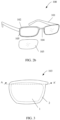
- FIG. 2a is a schematic diagram of a structure of a pair of smart glasses 100 according to an embodiment of this application.
- FIG. 2b is a schematic diagram of a structure of a locally separated part of the pair of smart glasses 100 according to an embodiment of this application.
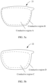
- FIG. 3 is a schematic diagram of a structure of a solar cell lens 103.
- the pair of smart glasses 100 includes glasses temples 101, glasses frames 102, solar cell lenses 103, and a cross beam 104, where the solar cell lens 103 is integrated with a solar cell.
- the solar cell lens 103 is embedded in a groove 105 of the glasses frame 102.
- a region covered by the groove 105 is visually opaque, and is defined as an external region 2 of the solar cell lens 103.
- a region not covered by the groove 105 is defined as an internal region 1 of the solar cell lens 103.
- a boundary between the external region 2 and the internal region 1 is distinguished by using a closed dashed dividing line. It should be understood that the dividing line is merely a schematic identification line, and the dividing line is not marked in an actual product.
- various power consumption modules 30 such as a battery, a processor, a sensor, and a communication module may be integrated in the glasses temple 101 or the glasses frame 102 based on a requirement.
- the solar cell integrated in the solar cell lens 103 is electrically connected to the power consumption modules 30 in the glasses temple 101 or the glasses frame 102 to supply power to the power consumption modules.
- the power consumption modules 30 are integrated in the glasses temple 101, and the solar cell is electrically connected to the power consumption modules 30 in the glasses temple 101, so that the solar cell supplies power to the power consumption modules 30 in the glasses temple 101.
- the solar cell may be electrically connected to the power consumption modules 30 in the glasses temple 101 through a hinge. However, this is not limited thereto.
- the glasses temple 101 may be folded, and states of the glasses temple 101 include an unfolded state and a folded state.
- the power consumption modules 30 are integrated in the glasses frame 102, and the solar cell is electrically connected to the power consumption modules 30 in the glasses frame 102, so that the solar cell supplies power to the power consumption modules 30 in the glasses frame 102.
- the sensor may be an azimuth sensor, a GPS (Global Positioning System) sensor, a temperature sensor, a touch sensor, an infrared sensor, or the like.
- the pair of smart glasses 100 of the structures shown in FIG. 2a and FIG. 2b is merely a structure in an implementation of this application.
- the structure of the pair of smart glasses 100 in this application is not limited to the structures shown in FIG. 2a and FIG. 2b .
- a structure of the glasses temple 101, a structure of the glasses frame 102, a fastening manner of the solar cell lens 103, and the like may be implemented in a plurality of forms.
- the glasses frame 102 may be disposed around the entire solar cell lens 103 as shown in FIG. 2a , namely, a full-frame structure.
- the glasses frame 102 may be disposed around only a part of a periphery of the solar cell lens 103, to be specific, only a part of the solar cell lens 103 is fixedly connected to the glasses frame 102, for example, a half-frame structure.
- the pair of smart glasses 100 may not be provided with a glasses frame 102, that is, has a frame-free structure.
- the another substrate may be specifically a commonly used solar cell substrate, for example, polyethylene terephthalate (PET).
- the solar cell 20 includes a front electrode 21, a back electrode 22, and a functional layer 23 stacked between the front electrode 21 and the back electrode 22, where the functional layer 23 includes a first carrier transport layer 231, a light absorption layer 232, and a second carrier transport layer 233 that are successively stacked, a material of the light absorption layer 232 absorbs photons and then is excited to generate electron-hole pairs, and the first carrier transport layer 231 and the second carrier transport layer 233 separately extract electrons or holes and transmit the electrons or holes to the front electrode 21 and the back electrode 22 for external power supply.
- the functional layer 23 includes a first carrier transport layer 231, a light absorption layer 232, and a second carrier transport layer 233 that are successively stacked
- a material of the light absorption layer 232 absorbs photons and then is excited to generate electron-hole pairs
- the front electrode 21 is an electrode on a side of an illuminated surface, and incident light is incident on the light absorption layer 232 from the front electrode 21.
- the back electrode 22 is an electrode on a side of a shady surface.
- the lens substrate 10 may be disposed on a side of the front electrode 21 (as shown in FIG. 4a ), or may be disposed on a side of the back electrode 22 (as shown in FIG. 4b ).
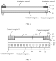
- the front electrode 21 of the solar cell 20 includes a low-conductivity region (namely, a conductive region A) and a high-conductivity region (namely, a conductive region B) disposed around the conductive region A.
- the back electrode 22 includes a low-conductivity region (namely, a conductive region C) and a high-conductivity region (namely, a conductive region D) disposed around the conductive region C.
- Conductivity of the conductive region B is higher than conductivity of the conductive region A
- conductivity of the conductive region D is higher than conductivity of the conductive region C.
- the front electrode and/or the back electrode may be designed to be separated by region and to include an internal conductive region and an external conductive region, and conductivity of the external conductive region is designed to be higher than conductivity of the internal conductive region.
- This can implement effective uniform convergence of a photocurrent of a front electrode and a back electrode in a large-area thin-film solar cell, avoid large-scale non-uniform lateral convergence of the photocurrent along surfaces of the front electrode and the back electrode, reduce a film loss and high dependence on film rectangular resistances of the front electrode and the back electrode, and improve photoelectric conversion efficiency of the cell.
- the design by region can improve cell comprehensive performance by flexibly selecting materials based on different requirements of different regions for performance, for example, transparency, in different application scenarios.
- the conductive region B is disposed around the conductive region A, and is in close contact with and electrically connected to the conductive region A.
- the conductive region B is configured to converge a photocurrent of the conductive region A.
- the conductive region B may completely surround the conductive region A as shown in FIG. 5a , or may partially surround the conductive region A.
- a size of the conductive region A is greater than the conductive region B.
- the conductive region D is disposed around the conductive region C, and is in close contact with and electrically connected to the conductive region C.
- the conductive region D is configured to converge a photocurrent of the conductive region C.
- the conductive region D may completely surround the conductive region C as shown in FIG.
- a degree of a conductivity difference between the conductive region B and the conductive region A is not limited, a degree of a conductivity difference between the conductive region D and the conductive region C is not limited, and the two degrees may be set based on an actual requirement.
- a larger degree of the conductivity difference is more conducive to convergence of photoelectrons.
- the conductivity of the conductive region B may be several to hundreds times higher than the conductivity of the conductive region A, for example, five times to 200 times.
- the conductivity of the conductive region D may be several to hundreds times higher than the conductivity of the conductive region C, for example, five times to 200 times.
- conductivity of each conductive region may be evaluated by using a film rectangular resistance of the conductive region.
- the film rectangular resistance is film rectangular resistance (Film rectangular resistance), and a unit is ⁇ / ⁇ .
- a higher film rectangular resistance of a conductive region indicates lower conductivity of the conductive region. Therefore, when a film rectangular resistance of the conductive region B is less than a film rectangular resistance of the conductive region A, the conductivity of the conductive region B is higher than the conductivity of the conductive region A.
- a film rectangular resistance of the conductive region D is less than a film rectangular resistance of the conductive region C, the conductivity of the conductive region D is higher than the conductivity of the conductive region C.
- the film rectangular resistance of the conductive region A may be several to hundreds times higher than the film rectangular resistance of the conductive region B, for example, five times to 200 times.
- the film rectangular resistance of the conductive region C may be several to hundreds times higher than the film rectangular resistance of the conductive region D, for example, five times to 200 times.
- the film rectangular resistance of the conductive region A may be 0.05 ⁇ / ⁇ to 20 ⁇ / ⁇ ; and the film rectangular resistance of the conductive region C may be 0.05 ⁇ / ⁇ to 20 ⁇ / ⁇ .
- the film rectangular resistance of the conductive region A may be 1 ⁇ / ⁇ to 10 ⁇ / ⁇ ; and the film rectangular resistance of the conductive region C may be 1 ⁇ / ⁇ to 10 ⁇ / ⁇ .
- the foregoing multiple range of five times to 200 times may be specifically, for example, five times, 10 times, 20 times, 50 times, 100 times, 150 times, or 200 times.
- a high-conductivity region is disposed around the cell to uniformly converge a photocurrent of an internal conductive region. This can effectively reduce a loss caused by large-scale non-uniform transfer of charges in a large-area thin-film solar cell, and improve photoelectric conversion efficiency of the cell.
- a material, a thickness, a region size, and the like of the conductive region B located at an external part in the front electrode 21 and a material, a thickness, a region size, and the like of the conductive region D located at an external part in the back electrode 22 may be set based on an actual application requirement.
- a width W f (as shown in FIG. 6 ) of the conductive region B should be set as small as possible, for example, the width of the conductive region B may be less than or equal to 1 mm.
- a width W r (as shown in FIG. 6 ) of the conductive region D may be determined based on a width of the groove in the glasses frame, to be specific, the conductive region D may be disposed completely or not completely corresponding to the external region 2 of the pair of smart glasses 100.
- the conductive region D is completely the same as the visually opaque external region 2 (namely, the groove region of the glasses frame) of the pair of smart glasses 100 in region shape and size, and projections of the two regions on a horizontal plane of the lens completely coincide, that is, the width of the conductive region D is equal to the width of the groove in the glasses frame.
- An enough high-conductivity region area can be ensured as far as possible by implementing complete corresponding, to improve cell efficiency.
- the width of the conductive region D may be less than or equal to 1 mm.
- the conductive region B may be completely the same as or different from the conductive region D in region size and shape. Widths at different positions of the conductive region B and the conductive region D may be the same or different.
- Visible light transmittance (Visible Light Transmittance, VLT) of the solar cell 20 may be adjusted based on materials, thicknesses, and the like of the functional layer and the back electrode.
- VLT of the internal region of the solar cell may be ⁇ %, where 0 ⁇ ⁇ ⁇ 100, and ⁇ may be adjusted based on materials and thicknesses of the back electrode and the functional layer in the internal region; and VLT of the external region of the solar cell may be ⁇ %, where ⁇ may be adjusted based on materials and thicknesses of the back electrode and the functional layer in the external region, and a value of ⁇ may meet 0 ⁇ ⁇ ⁇ .
- a transparency difference between the internal region and the external region of the solar cell can be implemented, so that a thin-film solar cell with mixed transparency is obtained, and maximization of light capture can be implemented by effectively using a scenario form feature.
- the front electrode 21 and the back electrode 22 may be combined with the functional layer 23 in a plurality of forms.
- the front electrode 21 and the back electrode 22 each include a conductive mesh layer structure
- the functional layer may be adversely affected if an electrode is directly manufactured on the functional layer 23. Therefore, to protect the functional layer 23, usually, a conductive mesh layer in an electrode that is first combined with the functional layer 23 is combined with the functional layer by using a planar conductive layer, and a conductive mesh layer in an electrode that is then combined with the functional layer is combined with the functional layer by using a conductive adhesive layer.
- the following performs description with an example in which the front electrode 21 is combined with the functional layer 23 first, and then the back electrode 22 is combined with the functional layer 23, that is, the front electrode 21, the functional layer 23, and the back electrode 22 are successively formed on the substrate.
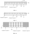
- the conductive region A of the front electrode 21 includes a transparent colloidal layer 201, a first conductive mesh layer 202 embedded in the transparent colloidal layer 201, and a planar conductive layer 203 disposed on the transparent colloidal layer 201 and the first conductive mesh layer 202.
- a thickness of the transparent colloidal layer 201 may be 2 ⁇ m to 20 ⁇ m
- a depth of the first conductive mesh layer 202 may be 1 ⁇ m to 10 ⁇ m
- a thickness of the planar conductive layer 203 may be 5 nm to 100 nm.
- the conductive region A is an internal part of the solar cell 20, namely, an intermediate region.
- this region can maintain high transparency while obtaining conductivity.
- the conductive meshes, transparent colloid, and the planar conductive layer are used to form the composite electrode, a film rectangular resistance loss can be reduced. This avoids a problem of a large film rectangular resistance loss caused by a transparent electrode that uses a TCO, a conductive polymer, or the like alone in a conventional solution.
- the conductive mesh material may alternatively only partially fill the mesh grooves, to be specific, the upper surface of the first conductive mesh layer 202 is lower than the upper surface of the transparent colloidal layer.
- a graphical structure form of the conductive mesh is not limited, and may be a regular graphical structure, for example, a quadrangle, a pentagon, a hexagon, or another polygon, or may be an irregular graphical structure. The graphical structure form may be specifically set based on an actual requirement.
- a contact area between the conductive mesh layer and the functional layer 23 is limited, electrical conduction of the electrode is limited.
- An area of a conductive surface that is of the electrode and that contacts the functional layer 23 of the cell can be enlarged by disposing the planar conductive layer 203 on the first conductive mesh layer 202. This improves performance of the cell.
- a material of the planar conductive layer 203 includes but is not limited to any one of or a combination of more of a transparent conductive oxide, a metal nanowire, a carbon nanotube, graphene, and a conductive polymer.
- the conductive region A of the front electrode 21 includes a transparent conductive oxide layer 201' and a first conductive mesh layer 202 embedded in the transparent conductive oxide layer 201'.
- a thickness of the transparent conductive oxide layer 201' may be 30 nm to 1000 nm. If the thickness of the transparent conductive oxide layer 201' is excessively large, transparency of the film layer decreases, and costs increase.
- one part of the first conductive mesh layer 202 may be embedded in PET or transparent colloid, and another part of the first conductive mesh layer 202 may be embedded in the transparent conductive oxide layer.
- the transparent colloidal layer in the conductive region B and the transparent colloidal layer 201 in the conductive region A have a same material selection range, and a material of the transparent colloidal layer in the conductive region B may be the same as or different from a material of the transparent colloidal layer in the conductive region A.
- the transparent conductive oxide layer in the conductive region B and the transparent conductive oxide layer in the conductive region A have a same material selection range, and a material of the transparent conductive oxide layer in the conductive region B may be the same as or different from a material of the transparent conductive oxide layer in the conductive region A.
- a material of the second conductive mesh layer 204 may be the same as or different from a material of the first conductive mesh layer 202.
- the first conductive mesh layer and the second conductive mesh layer are the same in material, mesh line width, and depth, the mesh period of the first conductive mesh layer is a square with a side length of 80 ⁇ m, and the mesh period of the second conductive mesh layer is a square with a side length of 20 ⁇ m.
- the conductive region B includes one or more of a metal layer or an alloy layer, a metal nanowire, graphene, a carbon nanotube, or a conductive polymer.
- the metal or alloy layer may include one or more of gold, silver, nickel, copper, aluminum, or the like.
- the metal or alloy layer may be of a single-layer structure including one metal or alloy, or may be of a multi-layer structure including a plurality of different metals or alloys.
- the conductive region B includes the metal or alloy layer, and the conductive region B is a metal electrode or an alloy electrode.
- the first layer 221 is a barrier layer
- the second layer 222 is the transparent conductive oxide layer.
- the barrier layer includes an organic barrier material and/or an inorganic barrier material. The film rectangular resistance loss can be reduced by using a composite electrode formed by the transparent conductive oxide and the organic or inorganic barrier layer.
- the organic barrier material includes but is not limited to copper phthalocyanine (CuPc), bathocuproine (BCP), and zinc phthalocyanine (ZnPc).
- the inorganic barrier material includes but is not limited to lithium metal (Li) and lithium fluoride.
- the conductive region C includes a thin metal or alloy, that is, the conductive region C uses a thin metal or alloy electrode.
- a thin metal or alloy layer may include one or more of gold, silver, nickel, copper, aluminum, or the like.
- the conductive region D may be transparent, semi-transparent, or opaque.
- a thickness of the conductive region D may be the same as or different from a thickness of the conductive region C.
- the conductive region D is designed to be opaque, a light loss can be reduced, and comprehensive photoelectric conversion efficiency of the large-area thin-film solar cell can be improved.
- the conductive region D is opaque and the conductive region C is semi-transparent, a thin-film solar cell with mixed transmittance can be formed.
- the conductive region D includes a transparent conductive oxide layer 226 and a fourth conductive mesh layer 227 embedded in the transparent conductive oxide layer 226, or includes a transparent colloidal layer 226 and a fourth conductive mesh layer 227 embedded in the transparent colloidal layer 226.
- the conductive region D is a transparent conductive mesh composite electrode embedded with transparent colloid or a transparent conductive oxide, and the transparent composite electrode may be manufactured in a transfer manner.
- the fourth conductive mesh layer 227 of the transparent composite electrode may implement mechanical bonding and close electrical contact with the functional layer 23 by using a conductive adhesive layer 225.
- a conductive mesh structure of the conductive region D may be manufactured together with that of the front electrode 21, thereby simplifying a conductive mesh layer manufacturing process.
- the conductive region D includes one or more of a metal layer or an alloy layer, a metal nanowire, graphene, a carbon nanotube, or a conductive polymer.
- the metal or alloy layer may include one or more of gold, silver, nickel, copper, aluminum, or the like.
- the metal or alloy layer may be of a single-layer structure including one metal or alloy, or may be of a multi-layer structure including a plurality of different metals or alloys.
- the conductive region B includes the metal or alloy layer, and the conductive region D is a metal electrode or an alloy electrode. The conductivity and transparency of the conductive region D can be adjusted by adjusting a thickness of a film layer.
- a conductive mesh layer of the front electrode is combined with the functional layer by using a planar conductive layer (the conductive mesh layer of the front electrode may be embedded in a transparent colloidal layer) or the functional layer is directly deposited on the conductive mesh layer to be in contact with, stacked with, and combined with the functional layer (the conductive mesh layer of the front electrode may be embedded in a transparent conductive oxide layer), and a conductive mesh layer of the back electrode is combined with the functional layer by using a conductive adhesive layer.
- a width W r of the conductive region D is the same as a width of a groove of a glasses frame of the pair of smart glasses, and W r is 1 mm. Conductivity of the conductive region D is greater than conductivity of the conductive region C.
- a functional layer includes an electron transport layer 231, a light absorption layer 232, and a hole transport layer 233, where the electron transport layer 231 is ZnO and has a thickness of 20 nm; the light absorption layer 232 uses PTB7-Th:IEICO-4F and has a thickness of 110 nm; and the hole transport layer 233 is molybdenum oxide MoOs and has a thickness of 3 nm.
- the conductive region A of the front electrode uses a transparent metal mesh-ITO (the planar conductive layer) composite electrode form.
- a transparent metal mesh-ITO the planar conductive layer
- the conductive region B of the front electrode and the conductive region D of the back electrode are respectively used as high-conductivity convergence regions of the front electrode and the back electrode.
- a manufacturing process can be simplified. By using a designed imprinting mold, the conductive region B and the conductive region D are manufactured while imprinting the conductive region A.
- the conductive region D of the back electrode is an Al electrode, a thickness of the Al layer is 150 nm, and a width Wr is 1 mm.
- the conductive region C of the back electrode uses a thin metal/metal oxide composite electrode, and in this embodiment, an Ag/MoO 3 composite electrode is used, where a thickness of Ag is 10 nm, and a thickness of MoOs is 35 nm. In this way, photoelectric conversion efficiency of a manufactured large-area device cell of 30 cm 2 is more than 2%.
- the conductive region D of the back electrode 22 is an Al electrode, a thickness of the Al layer is 110 nm, and a width Wr is 1 mm.
- the conductive region C of the back electrode 22 uses a composite electrode in which metal meshes 224 are embedded in a TCO layer 223, where a TCO uses ITO, a thickness of the ITO layer 223 is 300 nm, a mesh line width of the metal mesh 224 is 1 ⁇ m, a depth is 1 ⁇ m, a pattern is a regular hexagon, and a side length of the pattern is 85 ⁇ m. In this way, photoelectric conversion efficiency of a manufactured large-area device cell of 30 cm 2 is more than 2%.
- the conductive region D of the back electrode is an Al electrode, a thickness of the Al layer is 100 nm, and a width Wr is 1 mm.
- the conductive region C of the back electrode uses an Ag/MoO 3 thin metal/metal oxide composite electrode, where a thickness of an Ag layer is 10 nm, and a thickness of a MoOs layer is 35 nm.
- the conductive region B of the front electrode uses a form in which metal meshes are embedded in a transparent colloidal layer and a conductive modification layer is deposited on surfaces of the metal meshes, where the metal meshes use Ag/Cu metal meshes, a width of a trench is about 3.5 ⁇ m, a depth of the trench is about 3 ⁇ m, silver filling is performed for about 2.3 ⁇ m in the trench, and copper plating is performed for about 1.0 ⁇ m. After polishing is performed, a step is less than 10 nm, and a trench pattern is a regular hexagon with a side length of 85 ⁇ m.
- the conductive modification layer uses Ag, and has a thickness of 50 nm and a width W f of 1 mm.
- the trench in the conductive region B of the front electrode and a trench in the conductive region A of the front electrode are mutually connected.
- Parameters of the mesh trench and a metal mesh in the conductive region A of the front electrode are set the same as parameters of the trench and the metal mesh in the conductive region B. In this way, photoelectric conversion efficiency of a manufactured large-area device cell of 30 cm 2 is more than 2%.
- a semi-transparent thin-film solar cell structure includes stacked glass/indium tin oxide (ITO)/zinc oxide (ZnO)/PBTZT-stat-BDTT-8:PC61BM:PC71BM/PEDOT:PSS, where a front electrode is ITO, and a back electrode is PEDOT:PSS.
- ITO indium tin oxide
- ZnO zinc oxide
- PBTZT-stat-BDTT-8:PC61BM:PC71BM/PEDOT:PSS where a front electrode is ITO, and a back electrode is PEDOT:PSS.
- Average transmittance of a small-area device (0.24 cm 2 ) based on the structure is 24%, and photoelectric conversion efficiency under standard illuminance is 4.8%.
Landscapes
- Physics & Mathematics (AREA)
- General Physics & Mathematics (AREA)
- Optics & Photonics (AREA)
- Health & Medical Sciences (AREA)
- Engineering & Computer Science (AREA)
- Ophthalmology & Optometry (AREA)
- Otolaryngology (AREA)
- General Health & Medical Sciences (AREA)
- Acoustics & Sound (AREA)
- Power Engineering (AREA)
- Electromagnetism (AREA)
- Photovoltaic Devices (AREA)
- Life Sciences & Earth Sciences (AREA)
- Sustainable Development (AREA)
- Sustainable Energy (AREA)
Claims (14)
- Solarzelle, umfassend eine vordere Elektrode (21) und eine hintere Elektrode (22), die einander gegenüber angeordnet sind, und eine funktionelle Schicht (23), die zwischen der vorderen Elektrode (21) und der hinteren Elektrode (22) angeordnet ist, wobei die vordere Elektrode (21) eine Elektrode auf einer Seite einer beleuchteten Oberfläche ist, und die vordere Elektrode (21) eine Region mit hoher Leitfähigkeit (B) und eine Region mit niedriger Leitfähigkeit (A) umfasst, die benachbart zueinander sind, oder die hintere Elektrode (22) eine Region mit hoher Leitfähigkeit (D) und eine Region mit niedriger Leitfähigkeit (C) umfasst, die benachbart zueinander sind,
wobei die Region mit niedriger Leitfähigkeit (A) der vorderen Elektrode (21) eine transparente kolloidale Schicht (201) und eine erste leitfähige Maschenschicht (202) umfasst, die in die transparente kolloidale Schicht (201) eingebettet ist, oder eine transparente leitfähige Oxidschicht (201') und eine erste leitfähige Maschenschicht (202) umfasst, die in die transparente leitfähige Oxidschicht (201') eingebettet ist, wobei die erste leitfähige Maschenschicht (202) elektrisch mit der funktionellen Schicht (23) verbunden ist. - Solarzelle nach Anspruch 1, wobei die Region mit hoher Leitfähigkeit (B) der vorderen Elektrode (21) um die Region mit niedriger Leitfähigkeit (A) der vorderen Elektrode (21) angeordnet ist, oder die Region mit hoher Leitfähigkeit (D) der hinteren Elektrode (22) um die Region mit niedriger Leitfähigkeit (C) der hinteren Elektrode (22) angeordnet ist.
- Solarzelle nach Anspruch 2, wobei die Region mit hoher Leitfähigkeit (B) der vorderen Elektrode (21) die transparente kolloidale Schicht (201) und eine zweite leitfähige Maschenschicht (204) umfasst, die in die transparente kolloidale Schicht (201) eingebettet ist, oder die transparente leitfähige Oxidschicht (201') und eine zweite leitfähige Maschenschicht (204) umfasst, die in die transparente leitfähige Oxidschicht (201') eingebettet ist, wobei die zweite leitfähige Maschenschicht (204) elektrisch mit der funktionellen Schicht (23) verbunden ist.
- Solarzelle nach Anspruch 3, wobei die Flächendeckung der zweiten leitfähigen Maschenschicht (204) in der Region mit hoher Leitfähigkeit (B) der vorderen Elektrode (21) größer als die Flächendeckung der ersten leitfähigen Maschenschicht (202) in der Region mit niedriger Leitfähigkeit (A) der vorderen Elektrode (21) ist, oder ein Verhältnis von Tiefe zu Breite einer Maschenlinie der zweiten leitfähigen Maschenschicht (204) größer als ein Verhältnis von Tiefe zu Breite einer Maschenlinie der ersten leitfähigen Maschenschicht (204) ist.
- Solarzelle nach Anspruch 3, wobei die Region mit hoher Leitfähigkeit (B) der vorderen Elektrode (21) des Weiteren eine leitfähige Modifikationsschicht (205) umfasst, die auf der zweiten leitfähigen Maschenschicht (204) angeordnet ist.
- Solarzelle nach einem der Ansprüche 1 bis 5, wobei die vordere Elektrode (21) des Weiteren eine planare leitfähige Schicht (203) oder eine leitfähige Klebeschicht (225) umfasst, die zwischen der transparenten kolloidalen Schicht (201) und der funktionellen Schicht (23) angeordnet ist.
- Solarzelle nach einem der Ansprüche 1 bis 2, wobei die Region mit hoher Leitfähigkeit (B) der vorderen Elektrode (21) ein oder mehrere von einer Metallschicht oder einer Legierungsschicht, einem Metallnanodraht, Graphen, einem Kohlenstoffnanoröhrchen oder einem leitfähigen Polymer umfasst.
- Solarzelle nach einem der Ansprüche 1 bis 7, wobei die Region mit niedriger Leitfähigkeit (C) der hinteren Elektrode (22) eine Metallschicht oder eine Legierungsschicht umfasst, oder eine Metallschicht oder eine Legierungsschicht und eine transparente leitfähige Oxidschicht oder eine Metalloxidschicht gestapelt mit der Metall- oder Legierungsschicht umfasst, oder eine transparente leitfähige Oxidschicht (222) und eine Barriereschicht (221) umfasst, wobei die Metalloxidschicht ein oder mehrere von Molybdänoxid, Zinkoxid oder Wolframoxid umfasst, und die Barriereschicht ein organisches Barrierematerial und/oder ein anorganisches Barrierematerial umfasst.
- Solarzelle nach einem der Ansprüche 3 bis 7, wobei die Region mit niedriger Leitfähigkeit (C) der hinteren Elektrode (22) eine transparente kolloidale Schicht (201) und eine dritte leitfähige Maschenschicht (224) umfasst, die in die transparente kolloidale Schicht (201) eingebettet ist, oder eine transparente leitfähige Oxidschicht (201') und eine dritte leitfähige Maschenschicht (224) umfasst, die in die transparente leitfähige Oxidschicht (201') eingebettet ist, wobei die dritte leitfähige Maschenschicht (224) elektrisch mit der funktionellen Schicht (23) verbunden ist.
- Solarzelle nach einem der Ansprüche 3 bis 8, wobei die Region mit hoher Leitfähigkeit (D) der hinteren Elektrode (22) eine transparente kolloidale Schicht (201) und eine vierte leitfähige Maschenschicht (227) umfasst, die in die transparente kolloidale Schicht (201) eingebettet ist, oder eine transparente leitfähige Oxidschicht (201') und eine vierte leitfähige Maschenschicht (227) umfasst, die in die transparente leitfähige Oxidschicht (201') eingebettet ist, wobei die vierte leitfähige Maschenschicht (227) elektrisch mit der funktionellen Schicht (23) verbunden ist.
- Solarzelle nach Anspruch 9, wobei die Region mit hoher Leitfähigkeit (D) der hinteren Elektrode (22) die transparente kolloidale Schicht (201) und eine vierte leitfähige Maschenschicht (227) umfasst, die in die transparente kolloidale Schicht (201) eingebettet ist, oder die transparente leitfähige Oxidschicht (201') und eine vierte leitfähige Maschenschicht (227) umfasst, die in die transparente leitfähige Oxidschicht (201') eingebettet ist, wobei die vierte leitfähige Maschenschicht (227) elektrisch mit der funktionellen Schicht (23) verbunden ist.
- Solarzelle nach Anspruch 11, wobei die Flächendeckung der vierten leitfähigen Maschenschicht (227) in der Region mit hoher Leitfähigkeit (D) der hinteren Elektrode (22) größer als die Flächendeckung der dritten leitfähigen Maschenschicht (224) in der Region mit niedriger Leitfähigkeit (C) der hinteren Elektrode (22) ist, oder ein Verhältnis von Tiefe zu Breite einer Maschenlinie der vierten leitfähigen Maschenschicht (227) größer als ein Verhältnis von Tiefe zu Breite einer Maschenlinie der dritten leitfähigen Maschenschicht (224) ist.
- Solarzelle nach Anspruch 8 oder 9, wobei die Region mit hoher Leitfähigkeit (D) der hinteren Elektrode (22) ein oder mehrere von einer Metallschicht oder einer Legierungsschicht, einem Metallnanodraht, Graphen, einem Kohlenstoffnanoröhrchen oder einem leitfähigen Polymer umfasst.
- Elektronische Vorrichtung, umfassend die Solarzelle gemäß einem der Ansprüche 1 bis 14, wobei die Solarzelle ausgestaltet ist, die elektronische Vorrichtung mit Leistung zu versorgen.
Applications Claiming Priority (1)
| Application Number | Priority Date | Filing Date | Title |
|---|---|---|---|
| CN202110434235.1A CN113284957B (zh) | 2021-04-21 | 2021-04-21 | 太阳能电池和电子设备 |
Publications (3)
| Publication Number | Publication Date |
|---|---|
| EP4080587A1 EP4080587A1 (de) | 2022-10-26 |
| EP4080587C0 EP4080587C0 (de) | 2023-12-20 |
| EP4080587B1 true EP4080587B1 (de) | 2023-12-20 |
Family
ID=77277106
Family Applications (1)
| Application Number | Title | Priority Date | Filing Date |
|---|---|---|---|
| EP22169114.0A Active EP4080587B1 (de) | 2021-04-21 | 2022-04-20 | Solarzelle und elektronische vorrichtung |
Country Status (4)
| Country | Link |
|---|---|
| US (1) | US11961923B2 (de) |
| EP (1) | EP4080587B1 (de) |
| CN (1) | CN113284957B (de) |
| WO (1) | WO2022222953A1 (de) |
Families Citing this family (3)
| Publication number | Priority date | Publication date | Assignee | Title |
|---|---|---|---|---|
| CN113284957B (zh) | 2021-04-21 | 2022-09-23 | 华为技术有限公司 | 太阳能电池和电子设备 |
| EP4343857A4 (de) * | 2021-09-09 | 2024-08-07 | Huawei Technologies Co., Ltd. | Solarzellenvorrichtung und herstellungsverfahren dafür sowie elektronische vorrichtung |
| EP4485550A4 (de) * | 2022-08-18 | 2025-06-18 | Contemporary Amperex Technology Co., Limited | Solarzelle und herstellungsverfahren dafür |
Family Cites Families (15)
| Publication number | Priority date | Publication date | Assignee | Title |
|---|---|---|---|---|
| US4647711A (en) * | 1985-01-29 | 1987-03-03 | The Standard Oil Company | Stable front contact current collector for photovoltaic devices and method of making same |
| JP4325912B2 (ja) | 2003-02-14 | 2009-09-02 | 京セラ株式会社 | 太陽電池素子及びその製造方法 |
| FR2886419B1 (fr) * | 2005-05-27 | 2009-07-31 | Saint Gobain | Electrode de dispositifs electrochimiques/ electrocommandables |
| JP5913809B2 (ja) * | 2011-01-05 | 2016-04-27 | リンテック株式会社 | 透明電極基板、その製造方法、該透明電極基板を有する電子デバイス及び太陽電池 |
| US20150325717A1 (en) * | 2012-08-06 | 2015-11-12 | Dow Global Technologies Llc | High reliability photo-voltaic device |
| JP2014072492A (ja) * | 2012-10-01 | 2014-04-21 | Sharp Corp | 太陽電池、太陽電池パネル、及び太陽電池の製造方法 |
| CN103412662A (zh) * | 2013-03-30 | 2013-11-27 | 深圳欧菲光科技股份有限公司 | 触控面板及其制备方法 |
| CN104345514A (zh) * | 2013-07-25 | 2015-02-11 | 鸿富锦精密工业(深圳)有限公司 | 变色眼镜 |
| JP2015195341A (ja) * | 2014-03-24 | 2015-11-05 | 三菱電機株式会社 | 光電変換素子および光電変換素子の製造方法 |
| US20160126391A1 (en) * | 2014-10-31 | 2016-05-05 | Byd Company Limited | Solar cell module and manufacturing method thereof |
| CN107978646A (zh) * | 2016-10-17 | 2018-05-01 | 阿特斯阳光电力集团有限公司 | 太阳能电池片及太阳能电池组件 |
| US10156739B2 (en) * | 2017-02-14 | 2018-12-18 | International Business Machines Corporation | Ultraviolet-blocking photovoltaic sunglasses |
| US20180277692A1 (en) * | 2017-03-23 | 2018-09-27 | Kabushiki Kaisha Toshiba | Solar cell, multi-junction solar cell, solar cell module, and solar power generation system |
| CN109065757B (zh) * | 2018-08-07 | 2020-10-16 | 中国乐凯集团有限公司 | 用于oled照明器件的基板及照明器件 |
| CN113284957B (zh) * | 2021-04-21 | 2022-09-23 | 华为技术有限公司 | 太阳能电池和电子设备 |
-
2021
- 2021-04-21 CN CN202110434235.1A patent/CN113284957B/zh active Active
-
2022
- 2022-04-20 US US17/725,310 patent/US11961923B2/en active Active
- 2022-04-20 EP EP22169114.0A patent/EP4080587B1/de active Active
- 2022-04-20 WO PCT/CN2022/087888 patent/WO2022222953A1/zh not_active Ceased
Also Published As
| Publication number | Publication date |
|---|---|
| EP4080587A1 (de) | 2022-10-26 |
| EP4080587C0 (de) | 2023-12-20 |
| CN113284957A (zh) | 2021-08-20 |
| US20220344524A1 (en) | 2022-10-27 |
| CN113284957B (zh) | 2022-09-23 |
| US11961923B2 (en) | 2024-04-16 |
| WO2022222953A1 (zh) | 2022-10-27 |
Similar Documents
| Publication | Publication Date | Title |
|---|---|---|
| EP4080587B1 (de) | Solarzelle und elektronische vorrichtung | |
| CN105378940B (zh) | 薄层半透明光伏单电池 | |
| US11818903B2 (en) | Solar cell, and methods for preparing the solar cell, smart glasses, and electronic devices | |
| CN104412394B (zh) | 太阳能电池 | |
| US20210074870A1 (en) | Thin-film photovoltaic cell series structure and preparation process of thin-film photovoltaic cell series structure | |
| JP6656225B2 (ja) | 太陽電池およびその製造方法、ならびに太陽電池モジュール | |
| CN102782874B (zh) | 太阳能电池设备及其制造方法 | |
| US20130125980A1 (en) | Device for generating photovoltaic power and manufacturing method for same | |
| CN111525031A (zh) | 一种钙钛矿的三结叠层太阳能电池及其制备方法 | |
| US8981209B2 (en) | Photovoltaic module | |
| US20240274727A1 (en) | Solar cell component, manufacturing method thereof, and electronic device | |
| US20160087134A1 (en) | Solar cell apparatus and method of fabricating the same | |
| WO2021189841A1 (zh) | 一种具有触控功能的太阳能电池制造方法 | |
| CN104011876B (zh) | 太阳能电池装置及其制造方法 | |
| CN211350675U (zh) | 一种光伏电池环形串联结构 | |
| TW201442260A (zh) | 太陽能電池及其製造方法 | |
| CN210575971U (zh) | 一种光电转换率高的薄膜光伏电池 | |
| CN115802773A (zh) | 一种太阳能电池器件及其制造方法、电子设备 | |
| CN223310197U (zh) | 异质结电池和光伏组件 | |
| JP5935047B2 (ja) | 太陽電池、太陽電池モジュール及び太陽電池の製造方法 | |
| CN211265495U (zh) | 一种基于tft技术制作的太阳能电池 |
Legal Events
| Date | Code | Title | Description |
|---|---|---|---|
| PUAI | Public reference made under article 153(3) epc to a published international application that has entered the european phase |
Free format text: ORIGINAL CODE: 0009012 |
|
| STAA | Information on the status of an ep patent application or granted ep patent |
Free format text: STATUS: THE APPLICATION HAS BEEN PUBLISHED |
|
| AK | Designated contracting states |
Kind code of ref document: A1 Designated state(s): AL AT BE BG CH CY CZ DE DK EE ES FI FR GB GR HR HU IE IS IT LI LT LU LV MC MK MT NL NO PL PT RO RS SE SI SK SM TR |
|
| STAA | Information on the status of an ep patent application or granted ep patent |
Free format text: STATUS: REQUEST FOR EXAMINATION WAS MADE |
|
| 17P | Request for examination filed |
Effective date: 20230426 |
|
| RBV | Designated contracting states (corrected) |
Designated state(s): AL AT BE BG CH CY CZ DE DK EE ES FI FR GB GR HR HU IE IS IT LI LT LU LV MC MK MT NL NO PL PT RO RS SE SI SK SM TR |
|
| GRAP | Despatch of communication of intention to grant a patent |
Free format text: ORIGINAL CODE: EPIDOSNIGR1 |
|
| STAA | Information on the status of an ep patent application or granted ep patent |
Free format text: STATUS: GRANT OF PATENT IS INTENDED |
|
| RIC1 | Information provided on ipc code assigned before grant |
Ipc: H10K 30/81 20230101ALI20230616BHEP Ipc: H02S 30/00 20140101ALI20230616BHEP Ipc: G02C 11/00 20060101ALI20230616BHEP Ipc: G02B 27/01 20060101ALI20230616BHEP Ipc: H01L 31/0224 20060101AFI20230616BHEP |
|
| INTG | Intention to grant announced |
Effective date: 20230720 |
|
| GRAS | Grant fee paid |
Free format text: ORIGINAL CODE: EPIDOSNIGR3 |
|
| GRAA | (expected) grant |
Free format text: ORIGINAL CODE: 0009210 |
|
| STAA | Information on the status of an ep patent application or granted ep patent |
Free format text: STATUS: THE PATENT HAS BEEN GRANTED |
|
| REG | Reference to a national code |
Ref country code: DE Ref legal event code: R081 Ref document number: 602022001358 Country of ref document: DE Owner name: HUAWEI TECHNOLOGIES CO., LTD., SHENZHEN, CN Free format text: FORMER OWNER: HUAWEI TECHNOLOGIES CO., LTD., SHENZHEN, GUANGDONG, CN |
|
| AK | Designated contracting states |
Kind code of ref document: B1 Designated state(s): AL AT BE BG CH CY CZ DE DK EE ES FI FR GB GR HR HU IE IS IT LI LT LU LV MC MK MT NL NO PL PT RO RS SE SI SK SM TR |
|
| REG | Reference to a national code |
Ref country code: GB Ref legal event code: FG4D |
|
| REG | Reference to a national code |
Ref country code: CH Ref legal event code: EP |
|
| REG | Reference to a national code |
Ref country code: DE Ref legal event code: R096 Ref document number: 602022001358 Country of ref document: DE |
|
| REG | Reference to a national code |
Ref country code: IE Ref legal event code: FG4D |
|
| U01 | Request for unitary effect filed |
Effective date: 20231220 |
|
| U07 | Unitary effect registered |
Designated state(s): AT BE BG DE DK EE FI FR IT LT LU LV MT NL PT SE SI Effective date: 20240102 |
|
| PG25 | Lapsed in a contracting state [announced via postgrant information from national office to epo] |
Ref country code: GR Free format text: LAPSE BECAUSE OF FAILURE TO SUBMIT A TRANSLATION OF THE DESCRIPTION OR TO PAY THE FEE WITHIN THE PRESCRIBED TIME-LIMIT Effective date: 20240321 |
|
| PG25 | Lapsed in a contracting state [announced via postgrant information from national office to epo] |
Ref country code: ES Free format text: LAPSE BECAUSE OF FAILURE TO SUBMIT A TRANSLATION OF THE DESCRIPTION OR TO PAY THE FEE WITHIN THE PRESCRIBED TIME-LIMIT Effective date: 20231220 |
|
| PG25 | Lapsed in a contracting state [announced via postgrant information from national office to epo] |
Ref country code: GR Free format text: LAPSE BECAUSE OF FAILURE TO SUBMIT A TRANSLATION OF THE DESCRIPTION OR TO PAY THE FEE WITHIN THE PRESCRIBED TIME-LIMIT Effective date: 20240321 Ref country code: ES Free format text: LAPSE BECAUSE OF FAILURE TO SUBMIT A TRANSLATION OF THE DESCRIPTION OR TO PAY THE FEE WITHIN THE PRESCRIBED TIME-LIMIT Effective date: 20231220 |
|
| PG25 | Lapsed in a contracting state [announced via postgrant information from national office to epo] |
Ref country code: RS Free format text: LAPSE BECAUSE OF FAILURE TO SUBMIT A TRANSLATION OF THE DESCRIPTION OR TO PAY THE FEE WITHIN THE PRESCRIBED TIME-LIMIT Effective date: 20231220 Ref country code: NO Free format text: LAPSE BECAUSE OF FAILURE TO SUBMIT A TRANSLATION OF THE DESCRIPTION OR TO PAY THE FEE WITHIN THE PRESCRIBED TIME-LIMIT Effective date: 20240320 Ref country code: HR Free format text: LAPSE BECAUSE OF FAILURE TO SUBMIT A TRANSLATION OF THE DESCRIPTION OR TO PAY THE FEE WITHIN THE PRESCRIBED TIME-LIMIT Effective date: 20231220 |
|
| U20 | Renewal fee for the european patent with unitary effect paid |
Year of fee payment: 3 Effective date: 20240430 |
|
| PG25 | Lapsed in a contracting state [announced via postgrant information from national office to epo] |
Ref country code: IS Free format text: LAPSE BECAUSE OF FAILURE TO SUBMIT A TRANSLATION OF THE DESCRIPTION OR TO PAY THE FEE WITHIN THE PRESCRIBED TIME-LIMIT Effective date: 20240420 |
|
| PG25 | Lapsed in a contracting state [announced via postgrant information from national office to epo] |
Ref country code: CZ Free format text: LAPSE BECAUSE OF FAILURE TO SUBMIT A TRANSLATION OF THE DESCRIPTION OR TO PAY THE FEE WITHIN THE PRESCRIBED TIME-LIMIT Effective date: 20231220 |
|
| PG25 | Lapsed in a contracting state [announced via postgrant information from national office to epo] |
Ref country code: SK Free format text: LAPSE BECAUSE OF FAILURE TO SUBMIT A TRANSLATION OF THE DESCRIPTION OR TO PAY THE FEE WITHIN THE PRESCRIBED TIME-LIMIT Effective date: 20231220 |
|
| PG25 | Lapsed in a contracting state [announced via postgrant information from national office to epo] |
Ref country code: SM Free format text: LAPSE BECAUSE OF FAILURE TO SUBMIT A TRANSLATION OF THE DESCRIPTION OR TO PAY THE FEE WITHIN THE PRESCRIBED TIME-LIMIT Effective date: 20231220 Ref country code: SK Free format text: LAPSE BECAUSE OF FAILURE TO SUBMIT A TRANSLATION OF THE DESCRIPTION OR TO PAY THE FEE WITHIN THE PRESCRIBED TIME-LIMIT Effective date: 20231220 Ref country code: RO Free format text: LAPSE BECAUSE OF FAILURE TO SUBMIT A TRANSLATION OF THE DESCRIPTION OR TO PAY THE FEE WITHIN THE PRESCRIBED TIME-LIMIT Effective date: 20231220 Ref country code: IS Free format text: LAPSE BECAUSE OF FAILURE TO SUBMIT A TRANSLATION OF THE DESCRIPTION OR TO PAY THE FEE WITHIN THE PRESCRIBED TIME-LIMIT Effective date: 20240420 Ref country code: CZ Free format text: LAPSE BECAUSE OF FAILURE TO SUBMIT A TRANSLATION OF THE DESCRIPTION OR TO PAY THE FEE WITHIN THE PRESCRIBED TIME-LIMIT Effective date: 20231220 |
|
| PG25 | Lapsed in a contracting state [announced via postgrant information from national office to epo] |
Ref country code: PL Free format text: LAPSE BECAUSE OF FAILURE TO SUBMIT A TRANSLATION OF THE DESCRIPTION OR TO PAY THE FEE WITHIN THE PRESCRIBED TIME-LIMIT Effective date: 20231220 |
|
| PG25 | Lapsed in a contracting state [announced via postgrant information from national office to epo] |
Ref country code: PL Free format text: LAPSE BECAUSE OF FAILURE TO SUBMIT A TRANSLATION OF THE DESCRIPTION OR TO PAY THE FEE WITHIN THE PRESCRIBED TIME-LIMIT Effective date: 20231220 |
|
| REG | Reference to a national code |
Ref country code: DE Ref legal event code: R097 Ref document number: 602022001358 Country of ref document: DE |
|
| PLBE | No opposition filed within time limit |
Free format text: ORIGINAL CODE: 0009261 |
|
| STAA | Information on the status of an ep patent application or granted ep patent |
Free format text: STATUS: NO OPPOSITION FILED WITHIN TIME LIMIT |
|
| PG25 | Lapsed in a contracting state [announced via postgrant information from national office to epo] |
Ref country code: MC Free format text: LAPSE BECAUSE OF FAILURE TO SUBMIT A TRANSLATION OF THE DESCRIPTION OR TO PAY THE FEE WITHIN THE PRESCRIBED TIME-LIMIT Effective date: 20231220 |
|
| 26N | No opposition filed |
Effective date: 20240923 |
|
| PG25 | Lapsed in a contracting state [announced via postgrant information from national office to epo] |
Ref country code: MC Free format text: LAPSE BECAUSE OF FAILURE TO SUBMIT A TRANSLATION OF THE DESCRIPTION OR TO PAY THE FEE WITHIN THE PRESCRIBED TIME-LIMIT Effective date: 20231220 |
|
| PG25 | Lapsed in a contracting state [announced via postgrant information from national office to epo] |
Ref country code: IE Free format text: LAPSE BECAUSE OF NON-PAYMENT OF DUE FEES Effective date: 20240420 |
|
| U20 | Renewal fee for the european patent with unitary effect paid |
Year of fee payment: 4 Effective date: 20250430 |
|
| PG25 | Lapsed in a contracting state [announced via postgrant information from national office to epo] |
Ref country code: CY Free format text: LAPSE BECAUSE OF FAILURE TO SUBMIT A TRANSLATION OF THE DESCRIPTION OR TO PAY THE FEE WITHIN THE PRESCRIBED TIME-LIMIT; INVALID AB INITIO Effective date: 20220420 |
|
| PG25 | Lapsed in a contracting state [announced via postgrant information from national office to epo] |
Ref country code: HU Free format text: LAPSE BECAUSE OF FAILURE TO SUBMIT A TRANSLATION OF THE DESCRIPTION OR TO PAY THE FEE WITHIN THE PRESCRIBED TIME-LIMIT; INVALID AB INITIO Effective date: 20220420 |
|
| REG | Reference to a national code |
Ref country code: CH Ref legal event code: H13 Free format text: ST27 STATUS EVENT CODE: U-0-0-H10-H13 (AS PROVIDED BY THE NATIONAL OFFICE) Effective date: 20251125 |
|
| PG25 | Lapsed in a contracting state [announced via postgrant information from national office to epo] |
Ref country code: CH Free format text: LAPSE BECAUSE OF NON-PAYMENT OF DUE FEES Effective date: 20250430 |