EP4080566A1 - Method for restoring light emitting elements, and display panel comprising restored light emitting elements - Google Patents
Method for restoring light emitting elements, and display panel comprising restored light emitting elements Download PDFInfo
- Publication number
- EP4080566A1 EP4080566A1 EP20903706.8A EP20903706A EP4080566A1 EP 4080566 A1 EP4080566 A1 EP 4080566A1 EP 20903706 A EP20903706 A EP 20903706A EP 4080566 A1 EP4080566 A1 EP 4080566A1
- Authority
- EP
- European Patent Office
- Prior art keywords
- light emitting
- layer
- emitting devices
- pads
- bonding
- Prior art date
- Legal status (The legal status is an assumption and is not a legal conclusion. Google has not performed a legal analysis and makes no representation as to the accuracy of the status listed.)
- Pending
Links
Images



Classifications
-
- H—ELECTRICITY
- H10—SEMICONDUCTOR DEVICES; ELECTRIC SOLID-STATE DEVICES NOT OTHERWISE PROVIDED FOR
- H10W—GENERIC PACKAGES, INTERCONNECTIONS, CONNECTORS OR OTHER CONSTRUCTIONAL DETAILS OF DEVICES COVERED BY CLASS H10
- H10W90/00—Package configurations
-
- H—ELECTRICITY
- H10—SEMICONDUCTOR DEVICES; ELECTRIC SOLID-STATE DEVICES NOT OTHERWISE PROVIDED FOR
- H10W—GENERIC PACKAGES, INTERCONNECTIONS, CONNECTORS OR OTHER CONSTRUCTIONAL DETAILS OF DEVICES COVERED BY CLASS H10
- H10W72/00—Interconnections or connectors in packages
- H10W72/071—Connecting or disconnecting
-
- H—ELECTRICITY
- H10—SEMICONDUCTOR DEVICES; ELECTRIC SOLID-STATE DEVICES NOT OTHERWISE PROVIDED FOR
- H10H—INORGANIC LIGHT-EMITTING SEMICONDUCTOR DEVICES HAVING POTENTIAL BARRIERS
- H10H29/00—Integrated devices, or assemblies of multiple devices, comprising at least one light-emitting semiconductor element covered by group H10H20/00
- H10H29/10—Integrated devices comprising at least one light-emitting semiconductor component covered by group H10H20/00
- H10H29/14—Integrated devices comprising at least one light-emitting semiconductor component covered by group H10H20/00 comprising multiple light-emitting semiconductor components
- H10H29/142—Two-dimensional arrangements, e.g. asymmetric LED layout
-
- H—ELECTRICITY
- H10—SEMICONDUCTOR DEVICES; ELECTRIC SOLID-STATE DEVICES NOT OTHERWISE PROVIDED FOR
- H10D—INORGANIC ELECTRIC SEMICONDUCTOR DEVICES
- H10D86/00—Integrated devices formed in or on insulating or conducting substrates, e.g. formed in silicon-on-insulator [SOI] substrates or on stainless steel or glass substrates
- H10D86/40—Integrated devices formed in or on insulating or conducting substrates, e.g. formed in silicon-on-insulator [SOI] substrates or on stainless steel or glass substrates characterised by multiple TFTs
- H10D86/441—Interconnections, e.g. scanning lines
-
- H—ELECTRICITY
- H10—SEMICONDUCTOR DEVICES; ELECTRIC SOLID-STATE DEVICES NOT OTHERWISE PROVIDED FOR
- H10H—INORGANIC LIGHT-EMITTING SEMICONDUCTOR DEVICES HAVING POTENTIAL BARRIERS
- H10H20/00—Individual inorganic light-emitting semiconductor devices having potential barriers, e.g. light-emitting diodes [LED]
- H10H20/01—Manufacture or treatment
- H10H20/011—Manufacture or treatment of bodies, e.g. forming semiconductor layers
- H10H20/018—Bonding of wafers
-
- H—ELECTRICITY
- H10—SEMICONDUCTOR DEVICES; ELECTRIC SOLID-STATE DEVICES NOT OTHERWISE PROVIDED FOR
- H10H—INORGANIC LIGHT-EMITTING SEMICONDUCTOR DEVICES HAVING POTENTIAL BARRIERS
- H10H20/00—Individual inorganic light-emitting semiconductor devices having potential barriers, e.g. light-emitting diodes [LED]
- H10H20/01—Manufacture or treatment
- H10H20/036—Manufacture or treatment of packages
- H10H20/0364—Manufacture or treatment of packages of interconnections
-
- H—ELECTRICITY
- H10—SEMICONDUCTOR DEVICES; ELECTRIC SOLID-STATE DEVICES NOT OTHERWISE PROVIDED FOR
- H10H—INORGANIC LIGHT-EMITTING SEMICONDUCTOR DEVICES HAVING POTENTIAL BARRIERS
- H10H20/00—Individual inorganic light-emitting semiconductor devices having potential barriers, e.g. light-emitting diodes [LED]
- H10H20/80—Constructional details
- H10H20/85—Packages
- H10H20/857—Interconnections, e.g. lead-frames, bond wires or solder balls
-
- H—ELECTRICITY
- H10—SEMICONDUCTOR DEVICES; ELECTRIC SOLID-STATE DEVICES NOT OTHERWISE PROVIDED FOR
- H10H—INORGANIC LIGHT-EMITTING SEMICONDUCTOR DEVICES HAVING POTENTIAL BARRIERS
- H10H29/00—Integrated devices, or assemblies of multiple devices, comprising at least one light-emitting semiconductor element covered by group H10H20/00
- H10H29/01—Manufacture or treatment
- H10H29/036—Manufacture or treatment of packages
- H10H29/0364—Manufacture or treatment of packages of interconnections
-
- H—ELECTRICITY
- H10—SEMICONDUCTOR DEVICES; ELECTRIC SOLID-STATE DEVICES NOT OTHERWISE PROVIDED FOR
- H10H—INORGANIC LIGHT-EMITTING SEMICONDUCTOR DEVICES HAVING POTENTIAL BARRIERS
- H10H29/00—Integrated devices, or assemblies of multiple devices, comprising at least one light-emitting semiconductor element covered by group H10H20/00
- H10H29/20—Assemblies of multiple devices comprising at least one light-emitting semiconductor device covered by group H10H20/00
- H10H29/24—Assemblies of multiple devices comprising at least one light-emitting semiconductor device covered by group H10H20/00 comprising multiple light-emitting semiconductor devices
-
- H—ELECTRICITY
- H10—SEMICONDUCTOR DEVICES; ELECTRIC SOLID-STATE DEVICES NOT OTHERWISE PROVIDED FOR
- H10H—INORGANIC LIGHT-EMITTING SEMICONDUCTOR DEVICES HAVING POTENTIAL BARRIERS
- H10H29/00—Integrated devices, or assemblies of multiple devices, comprising at least one light-emitting semiconductor element covered by group H10H20/00
- H10H29/80—Constructional details
- H10H29/85—Packages
- H10H29/857—Interconnections
-
- H—ELECTRICITY
- H10—SEMICONDUCTOR DEVICES; ELECTRIC SOLID-STATE DEVICES NOT OTHERWISE PROVIDED FOR
- H10W—GENERIC PACKAGES, INTERCONNECTIONS, CONNECTORS OR OTHER CONSTRUCTIONAL DETAILS OF DEVICES COVERED BY CLASS H10
- H10W72/00—Interconnections or connectors in packages
- H10W72/20—Bump connectors, e.g. solder bumps or copper pillars; Dummy bumps; Thermal bumps
-
- H—ELECTRICITY
- H10—SEMICONDUCTOR DEVICES; ELECTRIC SOLID-STATE DEVICES NOT OTHERWISE PROVIDED FOR
- H10W—GENERIC PACKAGES, INTERCONNECTIONS, CONNECTORS OR OTHER CONSTRUCTIONAL DETAILS OF DEVICES COVERED BY CLASS H10
- H10W72/00—Interconnections or connectors in packages
- H10W72/01—Manufacture or treatment
- H10W72/0198—Manufacture or treatment batch processes
-
- H—ELECTRICITY
- H10—SEMICONDUCTOR DEVICES; ELECTRIC SOLID-STATE DEVICES NOT OTHERWISE PROVIDED FOR
- H10W—GENERIC PACKAGES, INTERCONNECTIONS, CONNECTORS OR OTHER CONSTRUCTIONAL DETAILS OF DEVICES COVERED BY CLASS H10
- H10W72/00—Interconnections or connectors in packages
- H10W72/071—Connecting or disconnecting
- H10W72/072—Connecting or disconnecting of bump connectors
-
- H—ELECTRICITY
- H10—SEMICONDUCTOR DEVICES; ELECTRIC SOLID-STATE DEVICES NOT OTHERWISE PROVIDED FOR
- H10W—GENERIC PACKAGES, INTERCONNECTIONS, CONNECTORS OR OTHER CONSTRUCTIONAL DETAILS OF DEVICES COVERED BY CLASS H10
- H10W72/00—Interconnections or connectors in packages
- H10W72/071—Connecting or disconnecting
- H10W72/072—Connecting or disconnecting of bump connectors
- H10W72/07202—Connecting or disconnecting of bump connectors using auxiliary members
- H10W72/07204—Connecting or disconnecting of bump connectors using auxiliary members using temporary auxiliary members, e.g. sacrificial coatings
-
- H—ELECTRICITY
- H10—SEMICONDUCTOR DEVICES; ELECTRIC SOLID-STATE DEVICES NOT OTHERWISE PROVIDED FOR
- H10W—GENERIC PACKAGES, INTERCONNECTIONS, CONNECTORS OR OTHER CONSTRUCTIONAL DETAILS OF DEVICES COVERED BY CLASS H10
- H10W72/00—Interconnections or connectors in packages
- H10W72/071—Connecting or disconnecting
- H10W72/072—Connecting or disconnecting of bump connectors
- H10W72/07251—Connecting or disconnecting of bump connectors characterised by changes in properties of the bump connectors during connecting
- H10W72/07255—Connecting or disconnecting of bump connectors characterised by changes in properties of the bump connectors during connecting changes in materials
-
- H—ELECTRICITY
- H10—SEMICONDUCTOR DEVICES; ELECTRIC SOLID-STATE DEVICES NOT OTHERWISE PROVIDED FOR
- H10W—GENERIC PACKAGES, INTERCONNECTIONS, CONNECTORS OR OTHER CONSTRUCTIONAL DETAILS OF DEVICES COVERED BY CLASS H10
- H10W72/00—Interconnections or connectors in packages
- H10W72/20—Bump connectors, e.g. solder bumps or copper pillars; Dummy bumps; Thermal bumps
- H10W72/241—Dispositions, e.g. layouts
-
- H—ELECTRICITY
- H10—SEMICONDUCTOR DEVICES; ELECTRIC SOLID-STATE DEVICES NOT OTHERWISE PROVIDED FOR
- H10W—GENERIC PACKAGES, INTERCONNECTIONS, CONNECTORS OR OTHER CONSTRUCTIONAL DETAILS OF DEVICES COVERED BY CLASS H10
- H10W72/00—Interconnections or connectors in packages
- H10W72/20—Bump connectors, e.g. solder bumps or copper pillars; Dummy bumps; Thermal bumps
- H10W72/251—Materials
-
- H—ELECTRICITY
- H10—SEMICONDUCTOR DEVICES; ELECTRIC SOLID-STATE DEVICES NOT OTHERWISE PROVIDED FOR
- H10W—GENERIC PACKAGES, INTERCONNECTIONS, CONNECTORS OR OTHER CONSTRUCTIONAL DETAILS OF DEVICES COVERED BY CLASS H10
- H10W72/00—Interconnections or connectors in packages
- H10W72/20—Bump connectors, e.g. solder bumps or copper pillars; Dummy bumps; Thermal bumps
- H10W72/251—Materials
- H10W72/252—Materials comprising solid metals or solid metalloids, e.g. PbSn, Ag or Cu
-
- H—ELECTRICITY
- H10—SEMICONDUCTOR DEVICES; ELECTRIC SOLID-STATE DEVICES NOT OTHERWISE PROVIDED FOR
- H10W—GENERIC PACKAGES, INTERCONNECTIONS, CONNECTORS OR OTHER CONSTRUCTIONAL DETAILS OF DEVICES COVERED BY CLASS H10
- H10W72/00—Interconnections or connectors in packages
- H10W72/20—Bump connectors, e.g. solder bumps or copper pillars; Dummy bumps; Thermal bumps
- H10W72/29—Bond pads specially adapted therefor
-
- H—ELECTRICITY
- H10—SEMICONDUCTOR DEVICES; ELECTRIC SOLID-STATE DEVICES NOT OTHERWISE PROVIDED FOR
- H10W—GENERIC PACKAGES, INTERCONNECTIONS, CONNECTORS OR OTHER CONSTRUCTIONAL DETAILS OF DEVICES COVERED BY CLASS H10
- H10W72/00—Interconnections or connectors in packages
- H10W72/90—Bond pads, in general
- H10W72/921—Structures or relative sizes of bond pads
- H10W72/923—Bond pads having multiple stacked layers
-
- H—ELECTRICITY
- H10—SEMICONDUCTOR DEVICES; ELECTRIC SOLID-STATE DEVICES NOT OTHERWISE PROVIDED FOR
- H10W—GENERIC PACKAGES, INTERCONNECTIONS, CONNECTORS OR OTHER CONSTRUCTIONAL DETAILS OF DEVICES COVERED BY CLASS H10
- H10W72/00—Interconnections or connectors in packages
- H10W72/90—Bond pads, in general
- H10W72/951—Materials of bond pads
-
- H—ELECTRICITY
- H10—SEMICONDUCTOR DEVICES; ELECTRIC SOLID-STATE DEVICES NOT OTHERWISE PROVIDED FOR
- H10W—GENERIC PACKAGES, INTERCONNECTIONS, CONNECTORS OR OTHER CONSTRUCTIONAL DETAILS OF DEVICES COVERED BY CLASS H10
- H10W90/00—Package configurations
- H10W90/701—Package configurations characterised by the relative positions of pads or connectors relative to package parts
- H10W90/721—Package configurations characterised by the relative positions of pads or connectors relative to package parts of bump connectors
- H10W90/724—Package configurations characterised by the relative positions of pads or connectors relative to package parts of bump connectors between a chip and a stacked insulating package substrate, interposer or RDL
Definitions
- Exemplary embodiments of the invention relate generally to a method of repairing light emitting devices, a display panel having the repaired light emitting device, and a display apparatus having the same.
- the exemplary embodiments relate to a method of repairing micro LEDs.
- light emitting diodes As an inorganic light source, light emitting diodes have been used in various fields including displays, vehicular lamps, general lighting, and the like. With various advantages of light emitting diodes over existing light sources, such as longer lifespan, lower power consumption, and rapid response, light emitting diodes have been replacing existing light sources.
- a display apparatus realizes various colors through mixture of blue, green and red light.
- the display apparatus includes a plurality of pixels, each of which comprises sub-pixels corresponding to blue, green and red light, respectively, in which a color of a certain pixel is determined based on the colors of the sub-pixels so that images can be displayed through combination of such pixels.
- LEDs can emit light of various colors depending on their materials, and a display apparatus in which individual micro LEDs emitting blue, green, and red are arranged on a two-dimensional plane, or a display apparatus in which micro LEDs having a stacked structure in which a blue LED, a green LED, and a red LED are stacked one above another are arranged on a two-dimensional plane may be provided.
- Micro LEDs used in one display apparatus usually require more than one million even for a small-sized display. Due to the small size of micro LEDs and the enormous number required, mass production of micro LED display apparatus with a conventional technology is almost impossible because a the conventional die bonding technology mounts LED chips individually mounted. Accordingly, a technology for transferring a plurality of micro LEDs onto a circuit board in a group has been recently developed.
- micro LEDs transferred in a group may exhibit poor bonding or poor luminescence characteristics, and these defective micro LEDs need to be repaired.
- repairment of micro LEDs includes replacing defective micro LEDs with normal micro LEDs, and repairment of micro LEDs is quite difficult because micro LEDs cannot be individually picked up and mounted due to the small size of the micro LEDs.
- Exemplary embodiments provide a new technology capable of repairing a light emitting device for a display, particularly micro LEDs.
- a display panel includes: a circuit board having first pads; a plurality of light emitting devices disposed on the circuit board, and having second pads; and a metal bonding layer bonding the first pads and the second pads, in which the plurality of light emitting devices includes at least one repaired light emitting device, and a metal bonding layer bonding the first pads and the second pads of the repaired light emitting device has a thickness or composition different from that of the metal bonding layer bonding the first pads and the second pads of the remaining light emitting devices.
- a method of repairing a light emitting device includes: removing a defective light emitting device among a plurality of light emitting devices transferred onto a circuit board; fabricating a light emitting device for repairing on a substrate; forming a bonding material layer on the light emitting device for repairing; and bonding the light emitting device for repairing to a location from which the defective light emitting device is removed using the bonding material layer.
- a display panel includes: a circuit board having first pads; a plurality of first light emitting devices disposed on the circuit board; first metal bonding layers bonding the first light emitting devices to the first pads; a lower barrier layer disposed between the first metal bonding layer and the first pad; and a lower metal layer disposed between the lower barrier layer and the first metal bonding layer, in which the first metal bonding layer is an alloy layer, and the lower metal layer is a metal layer having a different component from the first metal bonding layer.
- a display apparatus includes the display panel.
- a display panel includes: a circuit board having first pads; a plurality of light emitting devices disposed on the circuit board, and having second pads; and a metal bonding layer bonding the first pads and the second pads, in which the plurality of light emitting devices includes at least one repaired light emitting device, and a metal bonding layer bonding the first pads and the second pads of the repaired light emitting device has a thickness or composition different from that of the metal bonding layer bonding the first pads and the second pads of the remiaing light emitting devices.
- an upper surface of the repaired light emitting device may be placed at a higher elevation than those of the remaining light emitting devices.
- the metal bonding layer may include AuSn, CuSn, or In.
- each of the light emitting devices may emit light of any one color of blue light, green light, and red light.
- each of the light emitting devices may be configured to emit all of blue light, green light, and red light.
- a method of repairing a light emitting device includes: removing a defective light emitting device among a plurality of light emitting devices transferred onto a circuit board; fabricating a light emitting device for repairing on a substrate; forming a bonding material layer on the light emitting device for repairing; and bonding the light emitting device for repairing to a location from which the defective light emitting device is removed using the bonding material layers.
- the bonding material layer is formed on the light emitting device for repairing, the light emitting device for repairing may be easily bonded onto the circuit board.
- the bonding material layer may include In. Since In has a relatively low melting temperature, the light emitting device for repairing may be bonded without affecting other light emitting devices.
- Transferring the plurality of light emitting devices onto the circuit board may include: forming bonding material layers on first pads on the circuit board; disposing the plurality of light emitting devices on the bonding material layers; and forming metal bonding layers by applying heat to the bonding material layers.
- the metal bonding layer may be removed together, but the first pads may remain, and the light emitting device for repairing may be bonded to the remaining first pad.
- a plurality of light emitting devices for repairing may be manufactured together on the substrate, in which bonding material layers may be formed on the plurality of light emitting devices for repairing, respectively, a portion of the plurality of light emitting devices for repairing may be transferred onto a temporary substrate, the light emitting devices for repairing transferred onto the temporary substrate may be transferred onto a carrier substrate, and the light emitting devices for repairing on the carrier substrate may be bonded together using the bonding material layers at locations from which the defective light emitting devices are removed.
- the light emitting devices for repairing transferred onto the temporary substrate may be disposed corresponding to the locations from which the defective light emitting devices are removed.
- the carrier substrate may include an adhesive tape, and the light emitting devices for repairing may be transferred to the adhesive tape.
- a single light emitting device for repairing may be provided on the substrate, and the light emitting device for repairing on the substrate may be bonded to the location from which the defective light emitting device on the circuit board is removed.
- a plurality of defective light emitting devices on the circuit board may be repaired using a plurality of substrates on which the single light emitting devices for repairing are disposed, respectively.
- the method of repairing a light emitting device may further include forming barrier metal layers on the first pads before forming the bonding material layers on the first pads.
- the barrier metal layer may also be removed.
- the barrier metal layer may include a lower barrier metal layer and an upper barrier metal layer. Furthermore, when the metal bonding layer is removed, the upper barrier metal layer may also be removed, but the lower barrier metal layer may remain.
- a display panel includes: a circuit board having first pads; a plurality of first light emitting devices disposed on the circuit board; first metal bonding layers bonding the first light emitting devices to the first pads; a lower barrier layer disposed between the first metal bonding layer and the first pad; and a lower metal layer disposed between the lower barrier layer and the first metal bonding layer, in which the first metal bonding layer is an alloy layer, and the lower metal layer is a metal layer having a different component from the first metal bonding layer.
- the lower metal layer is included, when the first light emitting device is replaced with the second light emitting device for repairing, the lower metal layer may be mixed with the bonding material layer to form a bonding layer, thereby improving adhesion of the second light emitting device.
- the first metal bonding layers may include Au and In, and the lower metal layer may include Au.
- the lower metal layer may contact the lower barrier layer.
- the display panel may further include an upper barrier layer disposed between the first metal bonding layer and the lower metal layer.
- the upper barrier layer may contact the first metal bonding layer and the lower metal layer.
- the first light emitting device may include: second pads; and third barrier layers disposed on the second pads, in which the first metal bonding layer may be disposed between the lower metal layer and the third barrier layer.
- the display panel may further include: at least one second light emitting device disposed on the circuit board; and second metal bonding layers bonding the second light emitting device to the first pads, in which the second metal bonding layers may include a metallic element of the lower metal layer.
- the display panel may further include: a lower barrier layer disposed between the second metal bonding layer and the first pad, in which the lower barrier layer may contact the first pad and the second metal bonding layer.
- the display panel may further include an upper barrier layer disposed between the first metal bonding layer and the lower metal layer, in which the upper barrier layer may contact the first metal bonding layer.
- the second metal bonding layers may be thicker than the first metal bonding layers.
- an upper surface of the second light emitting device may be placed higher than that of the first light emitting device.
- the first and second light emitting devices may emit light of any one color of blue light, green light, and red light, respectively.
- the first and second light emitting devices may be configured to emit blue light, green light, and red light, respectively.
- a display apparatus includes the display panel.
- FIG. 1 shows schematic perspective views illustrating display apparatuses according to exemplary embodiments.
- the light emitting device is not particularly limited, but, particularly, it may be used in a VR display apparatus such as a smart watch 1000a or a VR headset 1000b, or an AR display apparatus such as augmented reality glasses 1000c.
- a VR display apparatus such as a smart watch 1000a or a VR headset 1000b
- an AR display apparatus such as augmented reality glasses 1000c.
- FIG. 2 is a schematic plan view illustrating a display panel 1000 according to an exemplary embodiment
- FIG. 3 is a schematic partial cross-sectional view taken along line A-A' of FIG. 2 .
- the display panel 1000 includes a circuit board 110 and light emitting devices 100 and 100a.
- the light emitting devices 100 and 100a may be small-sized LEDs, commonly referred to as micro LEDs.
- the light emitting device 100 may have a size smaller than 500 ⁇ m ⁇ 500 ⁇ m, and further, smaller than 100 ⁇ m ⁇ 100 ⁇ m.
- the inventive concepts do not limit the size of the light emitting device 100 to a specific size.
- the circuit board 110 may include a circuit for passive matrix driving or active matrix driving.
- the circuit board 110 may include interconnection lines and resistors therein.
- the circuit board 110 may include interconnection lines, transistors, and capacitors.
- the circuit board 110 may also have pads disposed on an upper surface thereof to allow electrical connection to the circuit therein.
- a plurality of light emitting devices 100 and 100a is arranged on the circuit board 110.
- the light emitting device 100 may refer to a light emitting device of good performance mounted on the circuit board 110 by group transfer, and the light emitting device 100a may refer to a repaired light emitting device.
- the repaired light emitting device 100a may have substantially the same structure as that of the light emitting device 100, but the inventive concepts are not limited thereto.
- An interval between the light emitting devices 100 and 100a may be at least greater than a width of a light emitting device 100.
- the light emitting devices 100 and 100a may be subpixels that emit light of a specific color, and these subpixels may form one pixel.
- a blue LED, a green LED, and a red LED may be disposed adjacent to one another to form one pixel.
- the inventive concepts are not limited thereto, and each of the light emitting devices 100 and 100a may have a stacked structure emitting light of various colors.
- each of the light emitting devices 100 and 100a may have a structure in which a blue LED, a green LED, and a red LED are stacked so as to overlap one another, and thus, one light emitting device may form one pixel.
- the light emitting device 100 may have pads 105, and the pads 105 may be adhered to corresponding pads 115 of the circuit board 110 through a bonding layer 120.
- the bonding layer 120 may include, for example, a bonding material such as AuSn, CuSn, In, or the like.
- the light emitting device 100a may have pads 105a, and the pads 105a may be adhered to corresponding pads 115a of the circuit board 110 through a bonding layer 120a.
- the pads 105a may be formed of the same material as the pads 105 and may have substantially the same layer structure, but the inventive concepts are not limited thereto.
- the pads 105 and 105a may be formed of different materials from each other, and may have different layer structures from each other.
- the pads 115a may be formed of substantially the same material as the pads 115 to have substantially the same layer structure, but the inventive concepts are not limited thereto.
- the material and structure of the pad 115a may be modified from those of the pad 115. This will be described in more detail later.
- an upper surface of the light emitting device 100a may be placed higher than that of the light emitting device 100.
- the bonding layer 120a may be thicker than the bonding layer 120, or the pad 105a may be thicker than the pad 105.
- a composition of the bonding layer 120a may be different from that of the bonding layer 120.
- Ni content of the bonding layer 120 may be higher than that of the bonding layer 120a.
- Au content of the bonding layer 120 may be higher than that of the bonding layer 120a.
- In content of the bonding layer 120a may be higher than that of the bonding layer 120.
- the display panel 1000 may include at least one light emitting device 100a, and the light emitting device 100a may be distinguished from the light emitting device 100, especially by the structure or composition of the bonding layer 120a, or by an elevation of the upper surface of the light emitting device 100a.
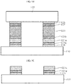
- FIGS. 4A, 4B , 4C, and 4D are schematic cross-sectional views illustrating a process of repairing a micro LED according to exemplary embodiments.
- a circuit board 110 includes pads 115.
- the pads 115 are connected to circuits in the circuit board 110 and provide contact points for connecting a light emitting device 100 to the circuits.
- the pads 115 are disposed in each region of the circuit board 110 where the light emitting devices 100 are to be mounted, such that a plurality of light emitting devices 100 may be mounted on the circuit board 110.
- the pads 115 may be formed of a metal layer including Au.
- the pads 115 may have a multilayer structure of Cu/Ni/Au.
- Barrier layers 121 are provided on the pads 115 and bonding material layers 123 are provided on the barrier layer 121.
- the barrier layers 121 may prevent the bonding material layers 123 from diffusing into the pads 115, thereby preventing damage to the pads 115.
- the barrier layer 121 may be a metal layer mixed with the bonding material layer 123, or may be a metal layer for blocking diffusion of the bonding material layer 123.
- the barrier layer 121 may include at least one metal selected from Ni, Cr, Ti, Ta, Mo, and W.
- the barrier layer 121 may have a multilayer structure of Cr/Ni or Ti/Ni.
- the bonding material layer 123 may include AuSn, CuSn, or In. In general, the bonding material layers 123 are provided on the pads 115 for group transfer using micro LED technology.
- a metal layer mixed with the bonding material layer 123 such as an Au layer may be interposed between the barrier layer 121 and the bonding material layer 123.
- the light emitting device 100 includes pads 105.
- the pads 105 correspond to the pads 115 on the circuit board 110.
- the pads 105 may be bump pads protruding from the light emitting device 100, but do not necessarily have a protruding shape.
- the plurality of light emitting devices 100 will be moved to locations of the corresponding pads 115 on the circuit board 110.
- a bonding layer 120 is formed by applying heat at a bonding temperature.
- the barrier layer 121 and the bonding material layer 123 may be mixed with each other, and at least a portion of the pads 105 may be mixed with the bonding material layer 123.
- the light emitting device 100 may be stably attached to the circuit board 110 by the bonding layer 120.
- a defect in the light emitting device 100 may be detected.
- the defect in the light emitting device 100 may be caused by, for example, defective bonding, or may be caused by a failure in performance of the light emitting device 100.
- the defective light emitting devices 100 are removed from the circuit board 110.
- the remaining bonding layers 120 and all of the barrier layers 121 may also be removed.
- the bonding layers 120 and the barrier layers 121 may be removed using a laser, for example.
- pads 115a may be retained on the circuit board 110 after the light emitting devices 100 are removed.
- the pads 115a may be the same as the pads 115 before bonding the light emitting devices 100, but may be modified from the pads 115.
- the pads 115a may include a metallic material for the bonding material layer 123.
- light emitting devices 100a for repairing are provided on the pads 115a.
- the light emitting devices 100a for repairing replace the defective light emitting devices 100, and may have performance required as the light emitting devices 100. Further, the light emitting device 100a may have substantially the same structure as a general structure of the light emitting device 100, but the inventive concepts are not limited thereto.
- the light emitting device 100a may have pads 105a.
- the pads 105a may have the same material and layer structure as those of the pads 105 described above, but the inventive concepts are not limited thereto.
- Bonding material layers 123a are provided on the pads 105a.
- the bonding material layer 123a may include a bonding material such as AuSn, CuSn, or In.
- the bonding material layer 123a has a melting point equal to or lower than that of the bonding material layer 123 described above.
- bonding layers 120a are formed by applying heat at a bonding temperature.
- the light emitting device 100a is bonded to the circuit board 110 by the bonding layer 120a.
- the bonding layer 120a may be configured to have the same composition as that of the bonding layer 120, but may be configured to have composition different from that of the bonding layer 120.
- the bonding material layers 123a are provided on the pads 105a of the light emitting device 100a for repairing so as to mount the light emitting device 100a on the circuit board 110 for repairing.
- the light emitting device 100 includes a micro LED which has a small size
- forming the bonding material layers 123a on the pads 115a of the circuit board 110 generally becomes very difficult due to their small form factor.
- forming the bonding material layers 123a may become easier, and thus, the light emitting device 100a for repairing may be easily mounted in a region where the defective light emitting device 100 is removed for repairing.
- FIGS. 5A, 5B, 5C , 5D, and 5E are schematic cross-sectional views illustrating a method of repairing a micro LED according to an exemplary embodiment.
- the substrate 21 may be a growth substrate for growing an epitaxial layer.
- the substrate 21 may be a sapphire substrate, a silicon substrate, or a GaAs substrate.
- the light emitting devices 100a may be manufactured using epitaxial layers grown on the substrate 21, and may include first conductivity type semiconductor layers, active layers, and second conductivity type semiconductor layers. Furthermore, the light emitting devices 100a may have a structure in which a plurality of LEDs is stacked.
- Each of the light emitting devices 100a has pads 105a, and bonding material layers 123a are provided on the pads 105a.
- the bonding material layers 123a may be provided by individually doping the bonding material layers 123a on the pads 105a, or the bonding material layers 123a may be formed on the pads 105a at once by dipping the pads 105a in a molten bonding material.
- the light emitting devices 100a for repairing are transferred onto a temporary substrate 210.
- the temporary substrate 210 may be a tape.
- the light emitting devices 100 are inspected to detect defective light emitting devices 100.
- the light emitting devices 100a for repairing are transferred onto the temporary substrate 210 to correspond to locations of the defective light emitting devices 100.
- the light emitting devices 100a for repairing may be separated from the substrate 21 using a selective laser lift-off technique.
- the light emitting devices 100a transferred onto the temporary substrate 210 are transferred again onto a carrier substrate 310.
- the carrier substrate 310 may have an adhesive tape 315 on a surface thereof.
- the adhesive tape 315 may also be formed of a material capable of being easily modified.
- the temporary substrate 210 is removed from the light emitting devices 100a, and thus, the bonding material layers 123a may be disposed on an opposite side of the carrier substrate 310.
- the bonding layers 120 may also be removed, and the pads 115a may remain. All of barrier layers 121 formed on the pads 115 may also be removed.
- the adhesive tape 315 on the carrier substrate 310 may be spaced apart from upper surfaces of the light emitting devices 100 mounted on the circuit board 110.
- the inventive concepts are not limited thereto, and the adhesive tape 315 may contact the light emitting devices 100. Subsequently, by applying heat to the bonding material layers 123a, the light emitting devices 100a are bonded to the circuit board 110
- a display panel having the repaired light emitting devices 100a is provided by separating the carrier substrate 310 from the light emitting devices 100a. Upper surfaces of the light emitting devices 100a may be placed substantially the same as or slightly higher than the upper surfaces of the light emitting devices 100.
- the light emitting devices 100 having defects may be replaced to the light emitting devices 100a for repairing through a single repairing process.
- FIGS. 6A, 6B , 6C, 6D, and 6E are schematic cross-sectional views illustrating a process of repairing a micro LED according to another exemplary embodiment.
- a light emitting device 100a for repairing is formed on a substrate 21a.
- a single light emitting device 100a is provided on the substrate 21a.
- a plurality of substrates 21a having single light emitting devices 100a may be provided.
- the substrate 21a may be a growth substrate for manufacturing the light emitting device 100a.
- the substrate 21a has a larger width than the light emitting device 100a, and thus, it is easier to handle the substrate 21a than the light emitting device 100a.
- the light emitting device 100a has pads 105a, and bonding material layers 123a are provided on the pads 105a.
- the light emitting device 100a is disposed and bonded on a circuit board 100a at a location where a defective light emitting device 100 is removed.
- the light emitting device 100a is difficult to handle because of a small size thereof, but the light emitting device 100a may be easily handled because of using the substrate 21a larger than the light emitting device 100a.
- a defective light emitting device 100 and a bonding layer 120 on the circuit board 110 are removed, so that pads 115a remain as described above.
- the bonding material layer 123a disposed on the light emitting device 100a for repairing is bonded to the pads 105a to form a bonding layer 120a, and the light emitting device 100a is bonded to the circuit board 110 by the bonding layer 120a.
- the substrate 21a is removed from the light emitting device 100a.
- the substrate 21a may be removed from the light emitting device 100a using, for example, a laser lift-off technique, a chemical etching technique, SLO, or the like.
- the light emitting device 100a for repairing is bonded to another location from which the defective light emitting device 100 is removed using the substrate 21a, and the substrate 21a is removed from the light emitting device 100a.
- All defective light emitting devices 100 on the circuit board 110 may be repaired by repeatedly performing the process of bonding the light emitting device 100a to the locations where the defective light emitting devices100 are removed using a plurality of substrates 21a each having the light emitting device 100a for repairing.
- an upper surface of the light emitting device 100a for repairing mounted on the circuit board 110 may be placed higher than that of the light emitting device 100. As such, damage to the light emitting devices 100 on the circuit board 110 by the substrate 21a may be prevented.
- the inventive concepts are not necessarily limited thereto, and elevations of upper surfaces of the light emitting devices 100 and 100a may be substantially the same.
- FIG. 7 is a schematic cross-sectional view illustrating a process of repairing a micro LED according to another exemplary embodiment.
- barrier layer 121 is interposed between the pad 115 and the bonding material layer 123 on the circuit board 110, but a plurality of barrier layers 121a and 121b are arranged in the exemplary embodiment.
- a lower barrier layer 121a, an intermediate layer 122, and an upper barrier layer 121b may be interposed between a pad 115 and a bonding material layer 123.
- the lower barrier layer 121a and the upper barrier layer 121b may include Ni, Cr, Ti, Ta, Mo, or W.
- the upper barrier layer 121b may include Ni that is easily mixed with the bonding material layer 123
- the lower barrier layer 121a may include Cr, Ti, Ta, Mo, or W that blocks the bonding material layer 123.
- the intermediate layer 122 may be a metal layer that separates the lower barrier layer 121a and the upper barrier layer 121b, and may be, for example, an Au layer.
- the intermediate layer 122 may be a metal layer that is easily mixed with the bonding material layer 123.
- a metal layer that is easily mixed with the bonding material layer 123 such as an Au layer, may be further disposed on the upper barrier layer 121b.
- the bonding layer 120 is also removed, and in this case, the upper barrier layer 121b is also removed.
- the lower barrier layer 121a may remain in the illustrated exemplary embodiment, and thus, damage to the pads 115 by the lower barrier layer 121a may be prevented.
- compositions of the bonding layer formed when the light emitting device 100 are bonded and the bonding layer formed when the light emitting devices 100a for repairing are bonded will be different from each other.
- metal bonding is generally formed by inter-mixing of metallic materials.
- the barrier layer may not be useful for alloy formation, and an alloy formation temperature may be high.
- an alloy layer formed already maintains a stable state, it is difficult to use the alloy layer again for metal bonding.
- a display panel suitable for bonding a light emitting device for repairing and a method of bonding a light emitting device for repairing will be described.
- FIG. 8 is a schematic partial cross-sectional view illustrating a display panel according to another exemplary embodiment.
- FIG. 8 is a cross-section taken along line A-A' of FIG. 2 .
- light emitting devices 100 and 100a may be small-sized LEDs, commonly referred to as micro LEDs.
- the light emitting devices 100 and 100a may have a size smaller than 500 ⁇ m ⁇ 500 ⁇ m, and further, smaller than 100 ⁇ m ⁇ 100 ⁇ m.
- the inventive concepts do not limit the size of the light emitting devices 100 and 100a to a specific size.
- a circuit board 110 may include a circuit for passive matrix driving or active matrix driving.
- the circuit board 110 may include interconnection lines and resistors therein.
- the circuit board 110 may include interconnection lines, transistors, and capacitors.
- the circuit board 110 may also have pads disposed on an upper surface thereof to allow electrical connection to the circuit therein.
- a plurality of light emitting devices 100 and 100a is arranged on the circuit board 110.
- the light emitting device 100 represents a light emitting device of good performance mounted on the circuit board 110 by group transfer, and the light emitting device 100a represents a light emitting device for repairing that replaces a defective light emitting device 100.
- a structure of the light emitting device 100a may be substantially the same as that of the light emitting device 100, but the inventive concepts are not limited thereto.
- an interval between the light emitting devices 100 and 100a may be wider than a width of one light emitting device 100.
- the light emitting devices 100 and 100a may be subpixels that emit light of a specific color, and these subpixels may constitute one pixel.
- a blue LED, a green LED, and a red LED may be adjacent to one another to constitute one pixel.
- the inventive concepts are not limited thereto, and each of the light emitting devices 100 and 100a may have a stacked structure emitting light of various colors.
- each of the light emitting devices 100 and 100a may have a structure in which a blue LED, a green LED, and a red LED are stacked so as to overlap one another, and thus, one light emitting device may constitute one pixel.
- the green LED may be disposed between the blue LED and the red LED.
- the blue LED may be disposed between the green LED and the red LED.
- brightness of the blue LED may be relatively reduced, and brightness of the green LED may be further increased, and thus, a mixing ratio of red, green, and blue may be easily adjusted.
- the light emitting device 100 may have pads 105, and the pads 105 may be adhered to corresponding pads 115 of the circuit board 110 through a bonding layer 220.
- the bonding layer 220 may include, for example, a bonding material such as Sn, In, or the like.
- the bonding layer 220 may be an alloy layer containing Au and In.
- a barrier layer 107 may be disposed between the bonding layer 220 and the pad 105.
- a material of the barrier layer 107 may be mixed with the bonding layer 220, thereby being dispersed in the bonding layer 220.
- a lower barrier layer 121a is disposed between the pad 115 and the bonding layer 220.
- the lower barrier layer 121a may contact the pad 115.
- the lower barrier layer 121a may include Ni, Cr, Ti, Ta, Mo, or W.
- a lower metal layer 221a may be disposed between the lower barrier layer 121a and the bonding layer 220.
- the lower metal layer 221a is spaced apart from the bonding layer 220, and thus, remains in a state unmixed with the bonding layer 220.
- the lower metal layer 221a may be formed of a metal layer, for example, Au, mixed with a bonding material layer such as Sn or In.
- the lower metal layer 221a may contact the lower barrier layer 121a.
- An upper barrier layer 121b may be disposed between the lower metal layer 221a and the bonding layer 220.
- the upper barrier layer 121b may include Ni, Cr, Ti, Ta, Mo, or W.
- the upper barrier layer 121b may be a metal layer of the same material as the lower barrier layer 121a, but the inventive concepts are not limited thereto.
- the upper barrier layer 121b may include Ni, Cr, Ti, Ta, Mo, or W suitable for blocking the bonding layer 220.
- the upper barrier layer 121b blocks the bonding layer 220 to prevent the lower metal layer 221a from being mixed with the bonding layer 220.
- the upper barrier layer 121b may contact the lower metal layer 221a.
- the light emitting device 100a may have pads 105a, and the pads 105a may be adhered to the corresponding pads 115 of the circuit board 110 through the bonding layer 220a.
- the pads 105a may be formed of the same material as the pads 105 and may have the same layer structure.
- the inventive concepts are not necessarily limited thereto, and may be formed of different materials from each other and may have different layer structures from each other.
- an upper surface of the light emitting device 100a may be placed higher than that of the light emitting device 100.
- the bonding layer 220a may be thicker than the bonding layer 220, or the pad 105a may be thicker than the pad 105.
- composition of the bonding layer 220a may be similar to that of the bonding layer 220.
- the bonding layer 220a includes a metallic component of the lower metal layer 221a.
- the bonding layer 220a may be an alloy layer in which Au and In are mixed.
- a content of each component of the bonding layer 220a may be different from that of each component of the bonding layer 220.
- a barrier layer 107a may be disposed between the pad 105a and the bonding layer 220a.
- the barrier layer 107a may be a metal layer of the same material as the barrier layer 107, but the inventive concepts are not limited thereto.
- a metallic material of the barrier layer 107a may be mixed with the bonding layer 220a and dispersed in the bonding layer 220a.
- the lower barrier layer 121a may remain between the pad 115 and the bonding layer 220a.
- the lower barrier layer 121a may include Cr, Ti, Ta, Mo, or W.
- the lower barrier layer 121a may be mixed with the bonding layer 220a and dispersed in the bonding layer 220a.
- the lower barrier layer 121a is formed of Ni, Ni may be dispersed in the bonding layer 220a.
- the lower metal layer 221a remains under the light emitting device 100, but the lower metal layer 221a does not remain under the light emitting device 100a. As such, when the light emitting device 100 is removed due to failure in bonding, the lower metal layer 221a may be used to bond the light emitting device 100a for repairing.
- FIGS. 9A , 9B , 9C , 9D, and 9E are schematic cross-sectional views illustrating a process of repairing a micro LED according to exemplary embodiments.
- a circuit board 110 includes pads 115.
- the pads 115 are connected to circuits in the circuit board 110 and provide contact points for connecting a light emitting device 100 to the circuits.
- the pads 115 are disposed on the circuit board 110 in each region where the light emitting devices 100 are to be mounted so as to mount a plurality of light emitting devices 100.
- the pads 115 may be formed of a metal layer containing Au.
- the pads 115 may have a multilayer structure of Cu/Ni/Au.
- a lower barrier layer 121a, a lower metal layer 221a, an upper barrier layer 121b, an upper metal layer 221b, and a bonding material layer 223 are provided on the pads 115.
- the lower barrier layer 121a is disposed between the pad 115 and the lower metal layer 221a.
- the lower metal layer 221a is separated from the upper metal layer 221b by the upper barrier layer 121a.
- the lower metal layer 221a may be formed of the same metal layer as the upper metal layer 221b, for example, an Au layer, but the inventive concepts are not limited thereto.
- the upper metal layer 221b may be formed of a metal layer that is mixed with the bonding material layer 223 to form an alloy during a bonding process.
- the bonding material layer 223 is formed of a material that forms a bonding layer by forming an alloy during the bonding process.
- the bonding material layer 223 may be formed of an In layer.
- the bonding material layers 223 are provided on the pads 115 for group transfer using micro LED technology.
- the upper barrier layer 121b prevents diffusion of a metal component of the bonding material layer 223 into the lower metal layer 221a.
- the upper barrier layer 121b may include, for example, at least one metal selected from Ni, Cr, Ti, Ta, Mo, and W.
- the barrier layer 121 may have a multilayer structure of Cr/Ni or Ti/Ni.
- the light emitting device 100 has pads 105.
- the pads 105 correspond to the pads 115 on the circuit board 110.
- the pads 105 may be bump pads protruding from the light emitting device 100, but do not necessarily have a protruding shape.
- the plurality of light emitting devices 100 will be moved to locations of the corresponding pads 115 on the circuit board 110.
- a barrier layer 107 and a metal layer 109 may be provided on the pads 105.
- the metal layer 109 may be formed of a metallic material that is mixed with the bonding material layer 223 to form an alloy.
- the barrier layer 107 protects the pad 105 while the bonding material layer 223 and the metal layer 109 form an alloy.
- the barrier layer 107 may include, for example, at least one metal selected from Ni, Cr, Ti, Ta, Mo, and W.
- a bonding layer 220 is formed by applying heat at a bonding temperature.
- the upper metal layer 221b, the bonding material layer 223, and the metal layer 109 may be mixed and alloyed to form the bonding layer 220.
- the bonding layer 220 may include a metal component of the bonding material layer 223, a metal component of the upper metal layer 221b, and a metal component of the metal layer 109.
- a thickness of the bonding material layer 223 and thicknesses of the upper metal layer 221b and the metal layer 109 may be controlled at an appropriate ratio.
- the bonding layer 220 is formed between the upper barrier layer 121b and the barrier layer 107.
- the light emitting device 100 may be stably attached to the circuit board 110 by the bonding layer 120.
- the upper barrier layer 121b prevents a metallic material of the bonding layer 220 from diffusing into the lower metal layer 221a to prevent alloying of the lower metal layer 221a.
- at least a portion of the upper barrier layer 121b may be mixed in the bonding layer 220 and dispersed.
- the barrier layer 107 may protect the pad 105 by blocking diffusion of the metallic material of the bonding layer 220 to the pad 105. However, at least a portion of the barrier layer 107 may be mixed in the bonding layer 220 and dispersed.
- a defect of the light emitting device 100 may be detected.
- the defect of the light emitting device 100 may be caused by, for example, defective bonding, or may be caused by a failure in performance of the light emitting device 100.
- the defective light emitting devices 100 are removed from the circuit board 110.
- the remaining bonding layers 220 may also be removed, and all of the barrier layers 121b may be removed.
- the bonding layers 220 and the barrier layers 121b may be removed using a laser. Accordingly, the lower metal layers 221a remain in upper portions of the pads 115 on the circuit board 110 after the light emitting devices 100 are removed.
- a light emitting device 100a for repairing is provided on the pads 115.
- the light emitting device 100a for repairing is for replacing the defective light emitting device 100, and may have performance required for the light emitting device 100. Further, the light emitting device 100a may have substantially the same structure as a general structure of the light emitting device 100, but the inventive concepts are not limited thereto.
- the light emitting device 100a may have pads 105a.
- the pads 105a may be the same in material and layer structure as the pads 105 described above, but the inventive concepts are not limited thereto.
- a barrier layer 107a, a metal layer 109a, and a bonding material layer 223a are provided on the pads 105a.
- the barrier layer 107a is provided to protect the pad 105a, and the metal layer 109a is provided together with the bonding material layer 223a to form a bonding layer.
- the bonding material layer 223a may include a bonding material such as Sn or In.
- the bonding material layer 223a has a melting point equal to or lower than that of the bonding material layer 223 described above.
- bonding layers 220a are formed by applying heat at a bonding temperature.
- the light emitting device 100a is bonded to the circuit board 110 by the bonding layer 220a.
- the bonding layer 220a may be formed by mixing the metal layer 109a, the lower metal layer 221a, and the bonding material layer 223a. Further, at least a portion of a metallic material of the lower barrier layer 121a or the barrier layer 107a may be mixed in the bonding layer 220a.
- the bonding layer 220a may be configured to have the same composition as the bonding layer 220, but may be configured to have composition different from that of the bonding layer 220.
- a method of bonding the light emitting device100a for repairing is similar to the method thereof described above with reference to FIGS. 5A to 5E or FIGS. 6A to 6E , and thus, repeated detailed descriptions thereof will be omitted to avoid redundancy.
- the lower metal layer 221a and the upper metal layer 221b are provided on the pad 115, and the lower metal layer 221a may be used to bond the light emitting device 100a for repairing, thereby improving adherence of the light emitting device 100a for repairing.
Landscapes
- Led Device Packages (AREA)
- Devices For Indicating Variable Information By Combining Individual Elements (AREA)
- Wire Bonding (AREA)
Abstract
Description
- Exemplary embodiments of the invention relate generally to a method of repairing light emitting devices, a display panel having the repaired light emitting device, and a display apparatus having the same. In particular, the exemplary embodiments relate to a method of repairing micro LEDs.
- As an inorganic light source, light emitting diodes have been used in various fields including displays, vehicular lamps, general lighting, and the like. With various advantages of light emitting diodes over existing light sources, such as longer lifespan, lower power consumption, and rapid response, light emitting diodes have been replacing existing light sources.
- Meanwhile, conventional light emitting diodes have been generally used as backlight light sources in display apparatuses. However, recently, small-sized light emitting diodes, that is, LED display apparatuses that directly implement an image using micro LEDs, have been developed.
- In general, a display apparatus realizes various colors through mixture of blue, green and red light. In order to display various images, the display apparatus includes a plurality of pixels, each of which comprises sub-pixels corresponding to blue, green and red light, respectively, in which a color of a certain pixel is determined based on the colors of the sub-pixels so that images can be displayed through combination of such pixels.
- LEDs can emit light of various colors depending on their materials, and a display apparatus in which individual micro LEDs emitting blue, green, and red are arranged on a two-dimensional plane, or a display apparatus in which micro LEDs having a stacked structure in which a blue LED, a green LED, and a red LED are stacked one above another are arranged on a two-dimensional plane may be provided.
- Micro LEDs used in one display apparatus usually require more than one million even for a small-sized display. Due to the small size of micro LEDs and the enormous number required, mass production of micro LED display apparatus with a conventional technology is almost impossible because a the conventional die bonding technology mounts LED chips individually mounted. Accordingly, a technology for transferring a plurality of micro LEDs onto a circuit board in a group has been recently developed.
- Some of the micro LEDs transferred in a group may exhibit poor bonding or poor luminescence characteristics, and these defective micro LEDs need to be repaired. In general, repairment of micro LEDs includes replacing defective micro LEDs with normal micro LEDs, and repairment of micro LEDs is quite difficult because micro LEDs cannot be individually picked up and mounted due to the small size of the micro LEDs.
- Exemplary embodiments provide a new technology capable of repairing a light emitting device for a display, particularly micro LEDs.
- A display panel according to an exemplary embodiment includes: a circuit board having first pads; a plurality of light emitting devices disposed on the circuit board, and having second pads; and a metal bonding layer bonding the first pads and the second pads, in which the plurality of light emitting devices includes at least one repaired light emitting device, and a metal bonding layer bonding the first pads and the second pads of the repaired light emitting device has a thickness or composition different from that of the metal bonding layer bonding the first pads and the second pads of the remaining light emitting devices.
- A method of repairing a light emitting device according to an exemplary embodiment includes: removing a defective light emitting device among a plurality of light emitting devices transferred onto a circuit board; fabricating a light emitting device for repairing on a substrate; forming a bonding material layer on the light emitting device for repairing; and bonding the light emitting device for repairing to a location from which the defective light emitting device is removed using the bonding material layer.
- A display panel according to an exemplary embodiment includes: a circuit board having first pads; a plurality of first light emitting devices disposed on the circuit board; first metal bonding layers bonding the first light emitting devices to the first pads; a lower barrier layer disposed between the first metal bonding layer and the first pad; and a lower metal layer disposed between the lower barrier layer and the first metal bonding layer, in which the first metal bonding layer is an alloy layer, and the lower metal layer is a metal layer having a different component from the first metal bonding layer.
- A display apparatus according to an exemplary embodiment includes the display panel.
-
-
FIG. 1 shows schematic perspective views illustrating display apparatuses according to exemplary embodiments. -
FIG. 2 is a schematic plan view illustrating a display panel according to an exemplary embodiment. -
FIG. 3 is a schematic partial cross-sectional view taken along line A-A' ofFIG. 2 illustrating a display panel according to an exemplary embodiment. -
FIGS. 4A, 4B ,4C, and 4D are schematic cross-sectional views illustrating a process of repairing a micro LED according to exemplary embodiments. -
FIGS. 5A, 5B, 5C ,5D, and 5E are schematic cross-sectional views illustrating a method of repairing a micro LED according to an exemplary embodiment. -
FIGS. 6A, 6B ,6C, 6D, and 6E are schematic cross-sectional views illustrating a process of repairing a micro LED according to another exemplary embodiment. -
FIG. 7 is a schematic cross-sectional view illustrating a process of repairing a micro LED according to another exemplary embodiment. -
FIG. 8 is a schematic plan view illustrating a display panel according to another exemplary embodiment. -
FIGS. 9A ,9B ,9C ,9D, and 9E are schematic cross-sectional views illustrating a process of repairing a micro LED according to exemplary embodiments. - Hereinafter, embodiments will be described in detail with reference to the accompanying drawings. The following embodiments are provided by way of example so as to fully convey the spirit of the present disclosure to those skilled in the art to which the present disclosure pertains. Accordingly, the present disclosure is not limited to the embodiments disclosed herein and can also be implemented in different forms. In the drawings, widths, lengths, thicknesses, and the like of devices can be exaggerated for clarity and descriptive purposes. When an element or layer is referred to as being "disposed above" or "disposed on" another element or layer, it can be directly "disposed above" or "disposed on" the other element or layer or intervening devices or layers can be present. Throughout the specification, like reference numerals denote like devices having the same or similar functions.
- A display panel according to an exemplary embodiment includes: a circuit board having first pads; a plurality of light emitting devices disposed on the circuit board, and having second pads; and a metal bonding layer bonding the first pads and the second pads, in which the plurality of light emitting devices includes at least one repaired light emitting device, and a metal bonding layer bonding the first pads and the second pads of the repaired light emitting device has a thickness or composition different from that of the metal bonding layer bonding the first pads and the second pads of the remiaing light emitting devices.
- In an exemplary embodiment, an upper surface of the repaired light emitting device may be placed at a higher elevation than those of the remaining light emitting devices.
- The metal bonding layer may include AuSn, CuSn, or In.
- In an exemplary embodiment, each of the light emitting devices may emit light of any one color of blue light, green light, and red light.
- In another exemplary embodiment, each of the light emitting devices may be configured to emit all of blue light, green light, and red light.
- A method of repairing a light emitting device according to an exemplary embodiment includes: removing a defective light emitting device among a plurality of light emitting devices transferred onto a circuit board; fabricating a light emitting device for repairing on a substrate; forming a bonding material layer on the light emitting device for repairing; and bonding the light emitting device for repairing to a location from which the defective light emitting device is removed using the bonding material layers.
- Since the bonding material layer is formed on the light emitting device for repairing, the light emitting device for repairing may be easily bonded onto the circuit board.
- The bonding material layer may include In. Since In has a relatively low melting temperature, the light emitting device for repairing may be bonded without affecting other light emitting devices.
- Transferring the plurality of light emitting devices onto the circuit board may include: forming bonding material layers on first pads on the circuit board; disposing the plurality of light emitting devices on the bonding material layers; and forming metal bonding layers by applying heat to the bonding material layers.
- Further, when the defective light emitting device is removed, the metal bonding layer may be removed together, but the first pads may remain, and the light emitting device for repairing may be bonded to the remaining first pad.
- In an exemplary embodiment, a plurality of light emitting devices for repairing may be manufactured together on the substrate, in which bonding material layers may be formed on the plurality of light emitting devices for repairing, respectively, a portion of the plurality of light emitting devices for repairing may be transferred onto a temporary substrate, the light emitting devices for repairing transferred onto the temporary substrate may be transferred onto a carrier substrate, and the light emitting devices for repairing on the carrier substrate may be bonded together using the bonding material layers at locations from which the defective light emitting devices are removed.
- Further, the light emitting devices for repairing transferred onto the temporary substrate may be disposed corresponding to the locations from which the defective light emitting devices are removed.
- In addition, the carrier substrate may include an adhesive tape, and the light emitting devices for repairing may be transferred to the adhesive tape.
- In another exemplary embodiment, a single light emitting device for repairing may be provided on the substrate, and the light emitting device for repairing on the substrate may be bonded to the location from which the defective light emitting device on the circuit board is removed.
- Further, a plurality of defective light emitting devices on the circuit board may be repaired using a plurality of substrates on which the single light emitting devices for repairing are disposed, respectively.
- Meanwhile, the method of repairing a light emitting device may further include forming barrier metal layers on the first pads before forming the bonding material layers on the first pads.
- In addition, when the metal bonding layer is removed, the barrier metal layer may also be removed.
- In an exemplary embodiment, the barrier metal layer may include a lower barrier metal layer and an upper barrier metal layer. Furthermore, when the metal bonding layer is removed, the upper barrier metal layer may also be removed, but the lower barrier metal layer may remain.
- A display panel according to an exemplary embodiment includes: a circuit board having first pads; a plurality of first light emitting devices disposed on the circuit board; first metal bonding layers bonding the first light emitting devices to the first pads; a lower barrier layer disposed between the first metal bonding layer and the first pad; and a lower metal layer disposed between the lower barrier layer and the first metal bonding layer, in which the first metal bonding layer is an alloy layer, and the lower metal layer is a metal layer having a different component from the first metal bonding layer.
- Since the lower metal layer is included, when the first light emitting device is replaced with the second light emitting device for repairing, the lower metal layer may be mixed with the bonding material layer to form a bonding layer, thereby improving adhesion of the second light emitting device.
- The first metal bonding layers may include Au and In, and the lower metal layer may include Au.
- Further, the lower metal layer may contact the lower barrier layer.
- The display panel may further include an upper barrier layer disposed between the first metal bonding layer and the lower metal layer. In addition, the upper barrier layer may contact the first metal bonding layer and the lower metal layer.
- The first light emitting device may include: second pads; and third barrier layers disposed on the second pads, in which the first metal bonding layer may be disposed between the lower metal layer and the third barrier layer.
- The display panel may further include: at least one second light emitting device disposed on the circuit board; and second metal bonding layers bonding the second light emitting device to the first pads, in which the second metal bonding layers may include a metallic element of the lower metal layer.
- In addition, the display panel may further include: a lower barrier layer disposed between the second metal bonding layer and the first pad, in which the lower barrier layer may contact the first pad and the second metal bonding layer.
- The display panel may further include an upper barrier layer disposed between the first metal bonding layer and the lower metal layer, in which the upper barrier layer may contact the first metal bonding layer.
- The second metal bonding layers may be thicker than the first metal bonding layers.
- In addition, an upper surface of the second light emitting device may be placed higher than that of the first light emitting device.
- In an exemplary embodiment, the first and second light emitting devices may emit light of any one color of blue light, green light, and red light, respectively.
- In another exemplary embodiment, the first and second light emitting devices may be configured to emit blue light, green light, and red light, respectively.
- A display apparatus according to an exemplary embodiment includes the display panel.
- Hereinafter, exemplary embodiments of the inventive concepts will be described in detail with reference to the accompanying drawings.
-
FIG. 1 shows schematic perspective views illustrating display apparatuses according to exemplary embodiments. - The light emitting device according to exemplary embodiments is not particularly limited, but, particularly, it may be used in a VR display apparatus such as a
smart watch 1000a or aVR headset 1000b, or an AR display apparatus such asaugmented reality glasses 1000c. - A display panel for implementing an image is mounted on a display apparatus.
FIG. 2 is a schematic plan view illustrating adisplay panel 1000 according to an exemplary embodiment, andFIG. 3 is a schematic partial cross-sectional view taken along line A-A' ofFIG. 2 . - Referring to
FIGS. 2 and 3 , thedisplay panel 1000 includes acircuit board 110 and light emittingdevices light emitting devices light emitting device 100 may have a size smaller than 500 µm ×500 µm, and further, smaller than 100 µm ×100 µm. However, the inventive concepts do not limit the size of thelight emitting device 100 to a specific size. - The
circuit board 110 may include a circuit for passive matrix driving or active matrix driving. In an exemplary embodiment, thecircuit board 110 may include interconnection lines and resistors therein. In another exemplary embodiment, thecircuit board 110 may include interconnection lines, transistors, and capacitors. Thecircuit board 110 may also have pads disposed on an upper surface thereof to allow electrical connection to the circuit therein. - A plurality of light emitting
devices circuit board 110. Thelight emitting device 100 may refer to a light emitting device of good performance mounted on thecircuit board 110 by group transfer, and thelight emitting device 100a may refer to a repaired light emitting device. The repairedlight emitting device 100a may have substantially the same structure as that of thelight emitting device 100, but the inventive concepts are not limited thereto. An interval between the light emittingdevices light emitting device 100. - In an exemplary embodiment, the
light emitting devices light emitting devices light emitting devices - The
light emitting device 100 may havepads 105, and thepads 105 may be adhered tocorresponding pads 115 of thecircuit board 110 through abonding layer 120. Thebonding layer 120 may include, for example, a bonding material such as AuSn, CuSn, In, or the like. - Meanwhile, the
light emitting device 100a may havepads 105a, and thepads 105a may be adhered tocorresponding pads 115a of thecircuit board 110 through abonding layer 120a. Thepads 105a may be formed of the same material as thepads 105 and may have substantially the same layer structure, but the inventive concepts are not limited thereto. Thepads pads 115a may be formed of substantially the same material as thepads 115 to have substantially the same layer structure, but the inventive concepts are not limited thereto. For example, the material and structure of thepad 115a may be modified from those of thepad 115. This will be described in more detail later. - In an exemplary embodiment, an upper surface of the
light emitting device 100a may be placed higher than that of thelight emitting device 100. In particular, thebonding layer 120a may be thicker than thebonding layer 120, or thepad 105a may be thicker than thepad 105. Furthermore, a composition of thebonding layer 120a may be different from that of thebonding layer 120. For example, Ni content of thebonding layer 120 may be higher than that of thebonding layer 120a. Furthermore, Au content of thebonding layer 120 may be higher than that of thebonding layer 120a. In addition, In content of thebonding layer 120a may be higher than that of thebonding layer 120. - The
display panel 1000 may include at least one light emittingdevice 100a, and thelight emitting device 100a may be distinguished from thelight emitting device 100, especially by the structure or composition of thebonding layer 120a, or by an elevation of the upper surface of thelight emitting device 100a. -
FIGS. 4A, 4B ,4C, and 4D are schematic cross-sectional views illustrating a process of repairing a micro LED according to exemplary embodiments. - Referring to
FIG. 4A , acircuit board 110 includespads 115. Thepads 115 are connected to circuits in thecircuit board 110 and provide contact points for connecting alight emitting device 100 to the circuits. Thepads 115 are disposed in each region of thecircuit board 110 where thelight emitting devices 100 are to be mounted, such that a plurality of light emittingdevices 100 may be mounted on thecircuit board 110. Thepads 115 may be formed of a metal layer including Au. For example, thepads 115 may have a multilayer structure of Cu/Ni/Au. - Barrier layers 121 are provided on the
pads 115 and bonding material layers 123 are provided on thebarrier layer 121. The barrier layers 121 may prevent the bonding material layers 123 from diffusing into thepads 115, thereby preventing damage to thepads 115. Thebarrier layer 121 may be a metal layer mixed with thebonding material layer 123, or may be a metal layer for blocking diffusion of thebonding material layer 123. For example, thebarrier layer 121 may include at least one metal selected from Ni, Cr, Ti, Ta, Mo, and W. For example, thebarrier layer 121 may have a multilayer structure of Cr/Ni or Ti/Ni. - The
bonding material layer 123 may include AuSn, CuSn, or In. In general, the bonding material layers 123 are provided on thepads 115 for group transfer using micro LED technology. - Meanwhile, although not shown in the drawing, a metal layer mixed with the
bonding material layer 123 such as an Au layer may be interposed between thebarrier layer 121 and thebonding material layer 123. - The
light emitting device 100 includespads 105. Thepads 105 correspond to thepads 115 on thecircuit board 110. As shown in the drawing, thepads 105 may be bump pads protruding from thelight emitting device 100, but do not necessarily have a protruding shape. The plurality of light emittingdevices 100 will be moved to locations of thecorresponding pads 115 on thecircuit board 110. - Referring to
FIG. 4B , after thepads 105 of thelight emitting device 100 are arranged on the bonding material layers 123 shown inFIG. 4A , abonding layer 120 is formed by applying heat at a bonding temperature. Thebarrier layer 121 and thebonding material layer 123 may be mixed with each other, and at least a portion of thepads 105 may be mixed with thebonding material layer 123. Thelight emitting device 100 may be stably attached to thecircuit board 110 by thebonding layer 120. - Referring to
FIG. 4C , as described with reference toFIG. 4B , after thelight emitting device 100 is bonded to thecircuit board 110, a defect in thelight emitting device 100 may be detected. The defect in thelight emitting device 100 may be caused by, for example, defective bonding, or may be caused by a failure in performance of thelight emitting device 100. - In this case, the defective
light emitting devices 100 are removed from thecircuit board 110. After thelight emitting devices 100 are removed, the remaining bonding layers 120 and all of the barrier layers 121 may also be removed. The bonding layers 120 and the barrier layers 121 may be removed using a laser, for example. Accordingly,pads 115a may be retained on thecircuit board 110 after thelight emitting devices 100 are removed. Thepads 115a may be the same as thepads 115 before bonding thelight emitting devices 100, but may be modified from thepads 115. For example, thepads 115a may include a metallic material for thebonding material layer 123. - Meanwhile, light emitting
devices 100a for repairing are provided on thepads 115a. Thelight emitting devices 100a for repairing replace the defectivelight emitting devices 100, and may have performance required as thelight emitting devices 100. Further, thelight emitting device 100a may have substantially the same structure as a general structure of thelight emitting device 100, but the inventive concepts are not limited thereto. - The
light emitting device 100a may havepads 105a. Thepads 105a may have the same material and layer structure as those of thepads 105 described above, but the inventive concepts are not limited thereto. -
Bonding material layers 123a are provided on thepads 105a. Thebonding material layer 123a may include a bonding material such as AuSn, CuSn, or In. In an exemplary embodiment, thebonding material layer 123a has a melting point equal to or lower than that of thebonding material layer 123 described above. - Referring to
FIG. 4D , after thebonding material layers 123a are arranged on thecorresponding pads 115a,bonding layers 120a are formed by applying heat at a bonding temperature. Thelight emitting device 100a is bonded to thecircuit board 110 by thebonding layer 120a. Thebonding layer 120a may be configured to have the same composition as that of thebonding layer 120, but may be configured to have composition different from that of thebonding layer 120. - In the illustrated exemplary embodiment, the
bonding material layers 123a are provided on thepads 105a of thelight emitting device 100a for repairing so as to mount thelight emitting device 100a on thecircuit board 110 for repairing. When thelight emitting device 100 includes a micro LED which has a small size, forming thebonding material layers 123a on thepads 115a of thecircuit board 110 generally becomes very difficult due to their small form factor. Howver, since thebonding material layers 123a are provided on thepads 105a of thelight emitting device 100a in the illustrated exemplary embodiment, forming thebonding material layers 123a may become easier, and thus, thelight emitting device 100a for repairing may be easily mounted in a region where the defectivelight emitting device 100 is removed for repairing. - Hereinafter, a method of repairing a micro LED according to exemplary embodiments will be described in detail.
-
FIGS. 5A, 5B, 5C ,5D, and 5E are schematic cross-sectional views illustrating a method of repairing a micro LED according to an exemplary embodiment. - First, referring to
FIG. 5A , light emittingdevices 100a for repairing may be arranged on asubstrate 21. Thesubstrate 21 may be a growth substrate for growing an epitaxial layer. For example, thesubstrate 21 may be a sapphire substrate, a silicon substrate, or a GaAs substrate. - The
light emitting devices 100a may be manufactured using epitaxial layers grown on thesubstrate 21, and may include first conductivity type semiconductor layers, active layers, and second conductivity type semiconductor layers. Furthermore, thelight emitting devices 100a may have a structure in which a plurality of LEDs is stacked. - Each of the
light emitting devices 100a haspads 105a, andbonding material layers 123a are provided on thepads 105a. For example, thebonding material layers 123a may be provided by individually doping thebonding material layers 123a on thepads 105a, or thebonding material layers 123a may be formed on thepads 105a at once by dipping thepads 105a in a molten bonding material. - Referring to
FIG. 5B , thelight emitting devices 100a for repairing are transferred onto atemporary substrate 210. Thetemporary substrate 210 may be a tape. After light emittingdevices 100 are transferred to thecircuit board 110 in a group, thelight emitting devices 100 are inspected to detect defectivelight emitting devices 100. Thelight emitting devices 100a for repairing are transferred onto thetemporary substrate 210 to correspond to locations of the defectivelight emitting devices 100. Thelight emitting devices 100a for repairing may be separated from thesubstrate 21 using a selective laser lift-off technique. - Referring to
FIG. 5C , thelight emitting devices 100a transferred onto thetemporary substrate 210 are transferred again onto acarrier substrate 310. Thecarrier substrate 310 may have anadhesive tape 315 on a surface thereof. Theadhesive tape 315 may also be formed of a material capable of being easily modified. - The
temporary substrate 210 is removed from thelight emitting devices 100a, and thus, thebonding material layers 123a may be disposed on an opposite side of thecarrier substrate 310. - Referring to
FIG. 5D , thecircuit board 110 from which the defectivelight emitting devices 100 are removed and thecarrier substrate 310 are moved to be close to each other, so that thelight emitting devices 100a are disposed at corresponding locations on thecircuit board 110. As described with reference toFIG. 4C , after the defectivelight emitting devices 100 are removed, the bonding layers 120 may also be removed, and thepads 115a may remain. All of barrier layers 121 formed on thepads 115 may also be removed. - Meanwhile, the
adhesive tape 315 on thecarrier substrate 310 may be spaced apart from upper surfaces of thelight emitting devices 100 mounted on thecircuit board 110. However, the inventive concepts are not limited thereto, and theadhesive tape 315 may contact thelight emitting devices 100. Subsequently, by applying heat to thebonding material layers 123a, thelight emitting devices 100a are bonded to thecircuit board 110 - Referring to
FIG. 5E , a display panel having the repairedlight emitting devices 100a is provided by separating thecarrier substrate 310 from thelight emitting devices 100a. Upper surfaces of thelight emitting devices 100a may be placed substantially the same as or slightly higher than the upper surfaces of thelight emitting devices 100. - According to the illustrated exemplary embodiment, among the
light emitting devices 100 disposed on thecircuit board 110, thelight emitting devices 100 having defects may be replaced to thelight emitting devices 100a for repairing through a single repairing process. -
FIGS. 6A, 6B ,6C, 6D, and 6E are schematic cross-sectional views illustrating a process of repairing a micro LED according to another exemplary embodiment. - First, referring to
FIG. 6A , alight emitting device 100a for repairing is formed on asubstrate 21a. In the exemplary embodiment, a singlelight emitting device 100a is provided on thesubstrate 21a. A plurality ofsubstrates 21a having singlelight emitting devices 100a may be provided. Thesubstrate 21a may be a growth substrate for manufacturing thelight emitting device 100a. Thesubstrate 21a has a larger width than thelight emitting device 100a, and thus, it is easier to handle thesubstrate 21a than thelight emitting device 100a. - As described above, the
light emitting device 100a haspads 105a, andbonding material layers 123a are provided on thepads 105a. - Referring to
FIG. 6B , thelight emitting device 100a is disposed and bonded on acircuit board 100a at a location where a defectivelight emitting device 100 is removed. Thelight emitting device 100a is difficult to handle because of a small size thereof, but thelight emitting device 100a may be easily handled because of using thesubstrate 21a larger than thelight emitting device 100a. - A defective
light emitting device 100 and abonding layer 120 on thecircuit board 110 are removed, so thatpads 115a remain as described above. Thebonding material layer 123a disposed on thelight emitting device 100a for repairing is bonded to thepads 105a to form abonding layer 120a, and thelight emitting device 100a is bonded to thecircuit board 110 by thebonding layer 120a. - Referring to
FIG. 6C , thesubstrate 21a is removed from thelight emitting device 100a. Thesubstrate 21a may be removed from thelight emitting device 100a using, for example, a laser lift-off technique, a chemical etching technique, SLO, or the like. - Referring to
FIGS. 6D and 6E , subsequently, thelight emitting device 100a for repairing is bonded to another location from which the defectivelight emitting device 100 is removed using thesubstrate 21a, and thesubstrate 21a is removed from thelight emitting device 100a. All defectivelight emitting devices 100 on thecircuit board 110 may be repaired by repeatedly performing the process of bonding thelight emitting device 100a to the locations where the defective light emitting devices100 are removed using a plurality ofsubstrates 21a each having thelight emitting device 100a for repairing. - In the exemplary embodiment, an upper surface of the
light emitting device 100a for repairing mounted on thecircuit board 110 may be placed higher than that of thelight emitting device 100. As such, damage to thelight emitting devices 100 on thecircuit board 110 by thesubstrate 21a may be prevented. However, the inventive concepts are not necessarily limited thereto, and elevations of upper surfaces of thelight emitting devices -
FIG. 7 is a schematic cross-sectional view illustrating a process of repairing a micro LED according to another exemplary embodiment. - Referring to
FIG. 7 , in the previous exemplary embodiments, it has been described that asingle barrier layer 121 is interposed between thepad 115 and thebonding material layer 123 on thecircuit board 110, but a plurality ofbarrier layers - That is, as shown in the drawing, a
lower barrier layer 121a, an intermediate layer 122, and anupper barrier layer 121b may be interposed between apad 115 and abonding material layer 123. Herein, thelower barrier layer 121a and theupper barrier layer 121b may include Ni, Cr, Ti, Ta, Mo, or W. As an example, theupper barrier layer 121b may include Ni that is easily mixed with thebonding material layer 123, and thelower barrier layer 121a may include Cr, Ti, Ta, Mo, or W that blocks thebonding material layer 123. The intermediate layer 122 may be a metal layer that separates thelower barrier layer 121a and theupper barrier layer 121b, and may be, for example, an Au layer. In particular, the intermediate layer 122 may be a metal layer that is easily mixed with thebonding material layer 123. - Further, a metal layer that is easily mixed with the
bonding material layer 123, such as an Au layer, may be further disposed on theupper barrier layer 121b. - When the
light emitting devices 100 are bonded,pads 105 of thelight emitting devices 100 are disposed on thebonding material layer 123 to form abonding layer 120. Thereafter, when a defectivelight emitting device 100 is removed, thebonding layer 120 is also removed, and in this case, theupper barrier layer 121b is also removed. However, unlike the previous exemplary embodiments, thelower barrier layer 121a may remain in the illustrated exemplary embodiment, and thus, damage to thepads 115 by thelower barrier layer 121a may be prevented. - In addition, according to the illustrated exemplary embodiment, when the
lower barrier layer 121a and theupper barrier layer 121b are formed of different metal layers from each other, compositions of the bonding layer formed when thelight emitting device 100 are bonded and the bonding layer formed when thelight emitting devices 100a for repairing are bonded will be different from each other. - Meanwhile, metal bonding is generally formed by inter-mixing of metallic materials. However, the barrier layer may not be useful for alloy formation, and an alloy formation temperature may be high. Meanwhile, since an alloy layer formed already maintains a stable state, it is difficult to use the alloy layer again for metal bonding. Hereinafter, a display panel suitable for bonding a light emitting device for repairing and a method of bonding a light emitting device for repairing will be described.
-
FIG. 8 is a schematic partial cross-sectional view illustrating a display panel according to another exemplary embodiment. Herein,FIG. 8 is a cross-section taken along line A-A' ofFIG. 2 . - Herein, light emitting
devices light emitting devices light emitting devices - A
circuit board 110 may include a circuit for passive matrix driving or active matrix driving. In an exemplary embodiment, thecircuit board 110 may include interconnection lines and resistors therein. In another exemplary embodiment, thecircuit board 110 may include interconnection lines, transistors, and capacitors. Thecircuit board 110 may also have pads disposed on an upper surface thereof to allow electrical connection to the circuit therein. - A plurality of light emitting
devices circuit board 110. Thelight emitting device 100 represents a light emitting device of good performance mounted on thecircuit board 110 by group transfer, and thelight emitting device 100a represents a light emitting device for repairing that replaces a defectivelight emitting device 100. A structure of thelight emitting device 100a may be substantially the same as that of thelight emitting device 100, but the inventive concepts are not limited thereto. In an exemplary embodiment, an interval between the light emittingdevices light emitting device 100. - In an exemplary embodiment, the
light emitting devices light emitting devices light emitting devices - The
light emitting device 100 may havepads 105, and thepads 105 may be adhered tocorresponding pads 115 of thecircuit board 110 through abonding layer 220. Thebonding layer 220 may include, for example, a bonding material such as Sn, In, or the like. In particular, thebonding layer 220 may be an alloy layer containing Au and In. - In an exemplary embodiment, a
barrier layer 107 may be disposed between thebonding layer 220 and thepad 105. In another exemplary embodiment, a material of thebarrier layer 107 may be mixed with thebonding layer 220, thereby being dispersed in thebonding layer 220. - Meanwhile, a
lower barrier layer 121a is disposed between thepad 115 and thebonding layer 220. Thelower barrier layer 121a may contact thepad 115. Thelower barrier layer 121a may include Ni, Cr, Ti, Ta, Mo, or W. - A
lower metal layer 221a may be disposed between thelower barrier layer 121a and thebonding layer 220. Thelower metal layer 221a is spaced apart from thebonding layer 220, and thus, remains in a state unmixed with thebonding layer 220. Thelower metal layer 221a may be formed of a metal layer, for example, Au, mixed with a bonding material layer such as Sn or In. Thelower metal layer 221a may contact thelower barrier layer 121a. - An
upper barrier layer 121b may be disposed between thelower metal layer 221a and thebonding layer 220. Theupper barrier layer 121b may include Ni, Cr, Ti, Ta, Mo, or W. Theupper barrier layer 121b may be a metal layer of the same material as thelower barrier layer 121a, but the inventive concepts are not limited thereto. In the illustrated exemplary embodiment, theupper barrier layer 121b may include Ni, Cr, Ti, Ta, Mo, or W suitable for blocking thebonding layer 220. Theupper barrier layer 121b blocks thebonding layer 220 to prevent thelower metal layer 221a from being mixed with thebonding layer 220. Theupper barrier layer 121b may contact thelower metal layer 221a. - The
light emitting device 100a may havepads 105a, and thepads 105a may be adhered to thecorresponding pads 115 of thecircuit board 110 through thebonding layer 220a. Thepads 105a may be formed of the same material as thepads 105 and may have the same layer structure. However, the inventive concepts are not necessarily limited thereto, and may be formed of different materials from each other and may have different layer structures from each other. - In an exemplary embodiment, an upper surface of the
light emitting device 100a may be placed higher than that of thelight emitting device 100. In particular, thebonding layer 220a may be thicker than thebonding layer 220, or thepad 105a may be thicker than thepad 105. Furthermore, composition of thebonding layer 220a may be similar to that of thebonding layer 220. In particular, thebonding layer 220a includes a metallic component of thelower metal layer 221a. For example, thebonding layer 220a may be an alloy layer in which Au and In are mixed. However, a content of each component of thebonding layer 220a may be different from that of each component of thebonding layer 220. - Meanwhile, a
barrier layer 107a may be disposed between thepad 105a and thebonding layer 220a. Thebarrier layer 107a may be a metal layer of the same material as thebarrier layer 107, but the inventive concepts are not limited thereto. In addition, a metallic material of thebarrier layer 107a may be mixed with thebonding layer 220a and dispersed in thebonding layer 220a. - In an exemplary embodiment, the
lower barrier layer 121a may remain between thepad 115 and thebonding layer 220a. In particular, thelower barrier layer 121a may include Cr, Ti, Ta, Mo, or W. In another exemplary embodiment, thelower barrier layer 121a may be mixed with thebonding layer 220a and dispersed in thebonding layer 220a. For example, when thelower barrier layer 121a is formed of Ni, Ni may be dispersed in thebonding layer 220a. - According to the illustrated exemplary embodiment, the
lower metal layer 221a remains under thelight emitting device 100, but thelower metal layer 221a does not remain under thelight emitting device 100a. As such, when thelight emitting device 100 is removed due to failure in bonding, thelower metal layer 221a may be used to bond thelight emitting device 100a for repairing. -
FIGS. 9A ,9B ,9C ,9D, and 9E are schematic cross-sectional views illustrating a process of repairing a micro LED according to exemplary embodiments. - Referring to
FIG. 9A , acircuit board 110 includespads 115. Thepads 115 are connected to circuits in thecircuit board 110 and provide contact points for connecting alight emitting device 100 to the circuits. Thepads 115 are disposed on thecircuit board 110 in each region where thelight emitting devices 100 are to be mounted so as to mount a plurality of light emittingdevices 100. Thepads 115 may be formed of a metal layer containing Au. For example, thepads 115 may have a multilayer structure of Cu/Ni/Au. - Meanwhile, a
lower barrier layer 121a, alower metal layer 221a, anupper barrier layer 121b, anupper metal layer 221b, and abonding material layer 223 are provided on thepads 115. Thelower barrier layer 121a is disposed between thepad 115 and thelower metal layer 221a. - The
lower metal layer 221a is separated from theupper metal layer 221b by theupper barrier layer 121a. Thelower metal layer 221a may be formed of the same metal layer as theupper metal layer 221b, for example, an Au layer, but the inventive concepts are not limited thereto. Theupper metal layer 221b may be formed of a metal layer that is mixed with thebonding material layer 223 to form an alloy during a bonding process. - The
bonding material layer 223 is formed of a material that forms a bonding layer by forming an alloy during the bonding process. For example, thebonding material layer 223 may be formed of an In layer. In general, the bonding material layers 223 are provided on thepads 115 for group transfer using micro LED technology. - The
upper barrier layer 121b prevents diffusion of a metal component of thebonding material layer 223 into thelower metal layer 221a. Theupper barrier layer 121b may include, for example, at least one metal selected from Ni, Cr, Ti, Ta, Mo, and W. For example, thebarrier layer 121 may have a multilayer structure of Cr/Ni or Ti/Ni. - Meanwhile, the
light emitting device 100 haspads 105. Thepads 105 correspond to thepads 115 on thecircuit board 110. As shown in the drawing, thepads 105 may be bump pads protruding from thelight emitting device 100, but do not necessarily have a protruding shape. The plurality of light emittingdevices 100 will be moved to locations of thecorresponding pads 115 on thecircuit board 110. - A
barrier layer 107 and ametal layer 109 may be provided on thepads 105. Themetal layer 109 may be formed of a metallic material that is mixed with thebonding material layer 223 to form an alloy. Thebarrier layer 107 protects thepad 105 while thebonding material layer 223 and themetal layer 109 form an alloy. Thebarrier layer 107 may include, for example, at least one metal selected from Ni, Cr, Ti, Ta, Mo, and W. - Referring to
FIG. 9B , after the metal layers 109 of thelight emitting device 100 are arranged on thebonding material layer 223 ofFIG. 9A , abonding layer 220 is formed by applying heat at a bonding temperature. Theupper metal layer 221b, thebonding material layer 223, and themetal layer 109 may be mixed and alloyed to form thebonding layer 220. As such, thebonding layer 220 may include a metal component of thebonding material layer 223, a metal component of theupper metal layer 221b, and a metal component of themetal layer 109. To form afavorable bonding layer 220, a thickness of thebonding material layer 223 and thicknesses of theupper metal layer 221b and themetal layer 109 may be controlled at an appropriate ratio. - According to the illustrated exemplary embodiment, the
bonding layer 220 is formed between theupper barrier layer 121b and thebarrier layer 107. Thelight emitting device 100 may be stably attached to thecircuit board 110 by thebonding layer 120. Theupper barrier layer 121b prevents a metallic material of thebonding layer 220 from diffusing into thelower metal layer 221a to prevent alloying of thelower metal layer 221a. However, at least a portion of theupper barrier layer 121b may be mixed in thebonding layer 220 and dispersed. - The
barrier layer 107 may protect thepad 105 by blocking diffusion of the metallic material of thebonding layer 220 to thepad 105. However, at least a portion of thebarrier layer 107 may be mixed in thebonding layer 220 and dispersed. - Referring to
FIG. 9C , as described with reference toFIG. 9B , after thelight emitting device 100 is bonded to thecircuit board 110, a defect of thelight emitting device 100 may be detected. The defect of thelight emitting device 100 may be caused by, for example, defective bonding, or may be caused by a failure in performance of thelight emitting device 100. - In this case, the defective
light emitting devices 100 are removed from thecircuit board 110. After thelight emitting devices 100 are removed, the remaining bonding layers 220 may also be removed, and all of the barrier layers 121b may be removed. For example, the bonding layers 220 and the barrier layers 121b may be removed using a laser. Accordingly, thelower metal layers 221a remain in upper portions of thepads 115 on thecircuit board 110 after thelight emitting devices 100 are removed. - Referring to
FIG. 9D , alight emitting device 100a for repairing is provided on thepads 115. Thelight emitting device 100a for repairing is for replacing the defectivelight emitting device 100, and may have performance required for thelight emitting device 100. Further, thelight emitting device 100a may have substantially the same structure as a general structure of thelight emitting device 100, but the inventive concepts are not limited thereto. - The
light emitting device 100a may havepads 105a. Thepads 105a may be the same in material and layer structure as thepads 105 described above, but the inventive concepts are not limited thereto. - Meanwhile, a
barrier layer 107a, ametal layer 109a, and abonding material layer 223a are provided on thepads 105a. Thebarrier layer 107a is provided to protect thepad 105a, and themetal layer 109a is provided together with thebonding material layer 223a to form a bonding layer. - The
bonding material layer 223a may include a bonding material such as Sn or In. In an exemplary embodiment, thebonding material layer 223a has a melting point equal to or lower than that of thebonding material layer 223 described above. - Referring to
FIG. 9E , after thebonding material layers 223a are arranged on thecorresponding pads 115,bonding layers 220a are formed by applying heat at a bonding temperature. Thelight emitting device 100a is bonded to thecircuit board 110 by thebonding layer 220a. Thebonding layer 220a may be formed by mixing themetal layer 109a, thelower metal layer 221a, and thebonding material layer 223a. Further, at least a portion of a metallic material of thelower barrier layer 121a or thebarrier layer 107a may be mixed in thebonding layer 220a. Thebonding layer 220a may be configured to have the same composition as thebonding layer 220, but may be configured to have composition different from that of thebonding layer 220. - Meanwhile, a method of bonding the light emitting device100a for repairing is similar to the method thereof described above with reference to
FIGS. 5A to 5E orFIGS. 6A to 6E , and thus, repeated detailed descriptions thereof will be omitted to avoid redundancy. - According to illustrated exemplary embodiment, the
lower metal layer 221a and theupper metal layer 221b are provided on thepad 115, and thelower metal layer 221a may be used to bond thelight emitting device 100a for repairing, thereby improving adherence of thelight emitting device 100a for repairing. - Although certain exemplary embodiments and implementations have been described herein, other embodiments and modifications will be apparent from this description. Accordingly, the inventive concepts are not limited to such embodiments, but rather to the broader scope of the appended claims and various obvious modifications and equivalent arrangements as would be apparent to a person of ordinary skill in the art.
Claims (35)
- A display panel, comprising:a circuit board having first pads;a plurality of light emitting devices disposed on the circuit board, and having second pads; anda metal bonding layer bonding the first pads and the second pads, wherein:the plurality of light emitting devices includes at least one repaired light emitting device, anda metal bonding layer bonding the first pads and the second pads of the light emitting device for repairing has a thickness or composition different from that of the metal bonding layer bonding the first pads and the second pads of other light emitting devices.
- The display panel of claim 1,
wherein an upper surface of the repaired light emitting device is placed at a higher elevation than those of the remaining light emitting devices. - The display panel of claim 1,
wherein the metal bonding layer includes AuSn, CuSn, or In. - The display panel of claim 1,
wherein each of the light emitting devices emits light of any one color of blue light, green light, and red light. - The display panel of claim 1,
wherein each of the light emitting devices is configured to emit all of blue light, green light, and red light. - A method of repairing a light emitting device, comprising:removing a defective light emitting device among a plurality of light emitting devices transferred onto a circuit board;fabricating a light emitting device for repairing on a substrate;forming a bonding material layer on the light emitting device for repairing; andbonding the light emitting device for repairing to a location from which the defective light emitting device is removed using the bonding material layer.
- The method of repairing light emitting devices of claim 6,
wherein the bonding material layer includes In. - The method of repairing light emitting devices of claim 6,
wherein transferring the plurality of light emitting devices onto the circuit board comprises:forming bonding material layers on first pads on the circuit board;disposing the plurality of light emitting devices on the bonding material layers; andforming metal bonding layers by applying heat to the bonding material layers. - The method of repairing light emitting devices of claim 8,
wherein, when the defective light emitting device is removed, the metal bonding layer is removed together, but the first pads remain, and the light emitting device for repairing is bonded to the remaining first pad. - The method of repairing light emitting devices of claim 8, wherein:a plurality of light emitting devices for repairing is manufactured together on the substrate,bonding material layers are formed on the plurality of light emitting devices for repairing, respectively,a portion of the plurality of light emitting devices for repairing is transferred onto a temporary substrate,the light emitting devices for repairing transferred onto the temporary substrate are transferred onto a carrier substrate, andthe light emitting devices for repairing on the carrier substrate are bonded together using the bonding material layers at locations from which the defective light emitting devices are removed.
- The method of repairing light emitting devices of claim 10,
wherein the light emitting devices for repairing transferred onto the temporary substrate are disposed corresponding to the locations from which the defective light emitting devices are removed. - The method of repairing light emitting devices of claim 10, wherein:the carrier substrate includes an adhesive tape, andthe light emitting devices for repairing are transferred to the adhesive tape.
- The method of repairing light emitting devices of claim 8, wherein:a single light emitting device for repairing is provided on the substrate, andthe light emitting device for repairing on the substrate is bonded to the location from which the defective light emitting device on the circuit board is removed.
- The method of repairing light emitting devices of claim 13,
wherein a plurality of defective light emitting devices on the circuit board is repaired using a plurality of substrates on which the single light emitting devices for repairing are disposed, respectively. - The method of repairing light emitting devices of claim 8, further comprising:
forming barrier metal layers on the first pads before forming the bonding material layers on the first pads. - The method of repairing light emitting devices of claim 15,
wherein, when the metal bonding layer is removed, the barrier metal layer is also removed. - The method of repairing light emitting devices of claim 15,
wherein the barrier metal layer includes a lower barrier metal layer and an upper barrier metal layer. - The method of repairing light emitting devices of claim 17,
wherein, when the metal bonding layer is removed, the upper barrier metal layer is also removed, but the lower barrier metal layer remains. - A display apparatus, comprising a display panel,
wherein the display panel includes:a circuit board having first pads;a plurality of light emitting devices disposed on the circuit board, and having second pads; anda metal bonding layer bonding the first pads and the second pads, wherein:the plurality of light emitting devices includes at least one repaired light emitting device, anda metal bonding layer bonding the first pads and the second pads of the repaired light emitting device has a thickness or composition different from that of the metal bonding layer bonding the first pads and the second pads of other light emitting devices. - The display apparatus of claim 19,
wherein an upper surface of the repaired light emitting device is placed at a higher elevation than those of the remaining light emitting devices. - A display panel, comprising:a circuit board having first pads;a plurality of first light emitting devices disposed on the circuit board;first metal bonding layers bonding the first light emitting devices to the first pads;a lower barrier layer disposed between the first metal bonding layer and the first pad; anda lower metal layer disposed between the lower barrier layer and the first metal bonding layer,wherein the first metal bonding layer is an alloy layer, and the lower metal layer is a metal layer having a different component from the first metal bonding layer.
- The display panel of claim 21, wherein:the first metal bonding layers include Au and In, andthe lower metal layer includes Au.
- The display panel of claim 21,
wherein the lower metal layer contacts the lower barrier layer. - The display panel of claim 21, further comprising:
an upper barrier layer disposed between the first metal bonding layer and the lower metal layer. - The display panel of claim 24,
wherein the upper barrier layer contacts the first metal bonding layer and the lower metal layer. - The display panel of claim 1, the first light emitting device, comprising:second pads; and third barrier layers disposed on the second pads,wherein the first metal bonding layer is disposed between the lower metal layer and the third barrier layer.
- The display panel of claim 1, further comprising:at least one second light emitting device disposed on the circuit board; andsecond metal bonding layers bonding the second light emitting device to the first pads,wherein the second metal bonding layers include a metallic element of the lower metal layer.
- The display panel of claim 27, further comprising:a lower barrier layer disposed between the second metal bonding layer and the first pad,wherein the lower barrier layer contacts the first pad and the second metal bonding layer.
- The display panel of claim 28, further comprising:an upper barrier layer disposed between the first metal bonding layer and the lower metal layer,wherein the upper barrier layer contacts the first metal bonding layer.
- The display panel of claim 27,
wherein the second metal bonding layers are thicker than the first metal bonding layers. - The display panel of claim 27,
wherein an upper surface of the second light emitting device is placed higher than that of the first light emitting device. - The display panel of claim 27,
wherein the first and second light emitting devices emit light of any one color of blue light, green light, and red light, respectively. - The display panel of claim 27,
wherein the first and second light emitting devices are configured to emit all of blue light, green light, and red light, respectively - A display apparatus, comprising a display panel,
wherein the display panel includes:a circuit board having first pads;a plurality of first light emitting devices disposed on the circuit board;first metal bonding layers bonding the first light emitting devices to the first pads;a lower barrier layer disposed between the first metal bonding layer and the first pad; anda lower metal layer disposed between the lower barrier layer and the first metal bonding layer,wherein the first metal bonding layer is an alloy layer, and the lower metal layer is a metal layer having a different component from the first metal bonding layer. - The display apparatus of claim 34, further comprising:at least one second light emitting device disposed on the circuit board; andsecond metal bonding layers bonding the second light emitting device to the first pads,wherein the second metal bonding layers include a metallic element of the lower metal layer.
Applications Claiming Priority (4)
| Application Number | Priority Date | Filing Date | Title |
|---|---|---|---|
| US201962949096P | 2019-12-17 | 2019-12-17 | |
| US202062991189P | 2020-03-18 | 2020-03-18 | |
| US17/121,651 US11508704B2 (en) | 2019-12-17 | 2020-12-14 | Method of repairing light emitting device and display panel having repaired light emitting device |
| PCT/KR2020/018430 WO2021125780A1 (en) | 2019-12-17 | 2020-12-16 | Method for restoring light emitting elements, and display panel comprising restored light emitting elements |
Publications (2)
| Publication Number | Publication Date |
|---|---|
| EP4080566A1 true EP4080566A1 (en) | 2022-10-26 |
| EP4080566A4 EP4080566A4 (en) | 2024-01-03 |
Family
ID=76320509
Family Applications (1)
| Application Number | Title | Priority Date | Filing Date |
|---|---|---|---|
| EP20903706.8A Pending EP4080566A4 (en) | 2019-12-17 | 2020-12-16 | METHOD FOR RESTORING LIGHT-EMITTING ELEMENTS AND DISPLAY PANEL COMPRISING RESTORED LIGHT-EMITTING ELEMENTS |
Country Status (6)
| Country | Link |
|---|---|
| US (3) | US11508704B2 (en) |
| EP (1) | EP4080566A4 (en) |
| JP (1) | JP7670719B2 (en) |
| KR (1) | KR102893348B1 (en) |
| CN (2) | CN213878148U (en) |
| WO (1) | WO2021125780A1 (en) |
Families Citing this family (10)
| Publication number | Priority date | Publication date | Assignee | Title |
|---|---|---|---|---|
| US11508704B2 (en) * | 2019-12-17 | 2022-11-22 | Seoul Viosys Co., Ltd. | Method of repairing light emitting device and display panel having repaired light emitting device |
| EP4375002A4 (en) * | 2021-07-20 | 2025-07-09 | Shinetsu Chemical Co | OPTICAL PROJECTION SYSTEM WITH SCAN REDUCTION AND LASER PROCESSING DEVICE THEREFOR |
| CN116031238A (en) | 2021-10-26 | 2023-04-28 | 群创光电股份有限公司 | electronic device |
| CN116190401A (en) * | 2021-11-26 | 2023-05-30 | 成都辰显光电有限公司 | Display panel and manufacturing method thereof |
| US20230387357A1 (en) * | 2022-05-26 | 2023-11-30 | Xiamen Extremely PQ Display Technology Co., Ltd. | Display panel, and light-emitting elements and backplate for display panel |
| CN218123408U (en) * | 2022-05-26 | 2022-12-23 | 厦门市芯颖显示科技有限公司 | A display panel, a light-emitting element and a backplane used for the display panel |
| JP7490848B2 (en) * | 2022-06-15 | 2024-05-27 | 信越化学工業株式会社 | Laser processing method, photomask and laser processing system |
| CN117597790A (en) * | 2022-06-17 | 2024-02-23 | 厦门市芯颖显示科技有限公司 | Microelectronic components, bonding backplanes and bonding assemblies |
| CN117476850A (en) * | 2022-07-22 | 2024-01-30 | 厦门市芯颖显示科技有限公司 | A kind of light-emitting element, backplane and display panel |
| EP4611024A1 (en) * | 2022-10-27 | 2025-09-03 | Kyocera Corporation | Device, electrical device, and substrate |
Family Cites Families (42)
| Publication number | Priority date | Publication date | Assignee | Title |
|---|---|---|---|---|
| US4857801A (en) * | 1983-04-18 | 1989-08-15 | Litton Systems Canada Limited | Dense LED matrix for high resolution full color video |
| TWI225899B (en) * | 2003-02-18 | 2005-01-01 | Unitive Semiconductor Taiwan C | Etching solution and method for manufacturing conductive bump using the etching solution to selectively remove barrier layer |
| US7271420B2 (en) | 2004-07-07 | 2007-09-18 | Cao Group, Inc. | Monolitholic LED chip to emit multiple colors |
| JP2008258459A (en) * | 2007-04-06 | 2008-10-23 | Toshiba Corp | Light emitting device and manufacturing method thereof |
| US8293587B2 (en) * | 2007-10-11 | 2012-10-23 | International Business Machines Corporation | Multilayer pillar for reduced stress interconnect and method of making same |
| US8230690B1 (en) * | 2008-05-20 | 2012-07-31 | Nader Salessi | Modular LED lamp |
| CN102144261A (en) * | 2008-10-24 | 2011-08-03 | 松下电器产业株式会社 | Optical unit and electronic device using same |
| JP5663607B2 (en) * | 2011-02-10 | 2015-02-04 | パナソニックIpマネジメント株式会社 | Semiconductor device |
| CN102903804B (en) * | 2011-07-25 | 2015-12-16 | 财团法人工业技术研究院 | Light-emitting element transfer method and light-emitting element array |
| US8349116B1 (en) * | 2011-11-18 | 2013-01-08 | LuxVue Technology Corporation | Micro device transfer head heater assembly and method of transferring a micro device |
| US8933433B2 (en) * | 2012-07-30 | 2015-01-13 | LuxVue Technology Corporation | Method and structure for receiving a micro device |
| US8803337B1 (en) * | 2013-03-14 | 2014-08-12 | Taiwan Semiconductor Manufacturing Company, Ltd. | Integrated circuit structure having dies with connectors |
| CN104752458B (en) * | 2013-12-25 | 2017-12-22 | 清华大学 | The preparation method of organic LED array |
| JP6152816B2 (en) | 2014-03-26 | 2017-06-28 | ソニー株式会社 | SEMICONDUCTOR DEVICE, DISPLAY PANEL, DISPLAY DEVICE, ELECTRONIC DEVICE, AND SEMICONDUCTOR DEVICE MANUFACTURING METHOD |
| JP6128046B2 (en) | 2014-03-31 | 2017-05-17 | ソニー株式会社 | Mounting board and electronic equipment |
| US9793248B2 (en) * | 2014-11-18 | 2017-10-17 | PlayNitride Inc. | Light emitting device |
| US9478583B2 (en) | 2014-12-08 | 2016-10-25 | Apple Inc. | Wearable display having an array of LEDs on a conformable silicon substrate |
| WO2016100657A2 (en) * | 2014-12-19 | 2016-06-23 | Glo Ab | Method of making a light emitting diode array on a backplane |
| TWI557702B (en) * | 2015-06-01 | 2016-11-11 | 友達光電股份有限公司 | Display panel and its repair method |
| US10886250B2 (en) * | 2015-07-10 | 2021-01-05 | Invensas Corporation | Structures and methods for low temperature bonding using nanoparticles |
| CN107251237B (en) | 2015-08-18 | 2019-12-13 | 歌尔股份有限公司 | Micro light emitting diode repair method, manufacturing method, device and electronic equipment |
| US10468361B2 (en) * | 2015-08-27 | 2019-11-05 | Mikro Mesa Technology Co., Ltd. | Method of manufacturing light emitting diodes having a supporting layer attached to temporary adhesive |
| JP6639188B2 (en) | 2015-10-21 | 2020-02-05 | ソニーセミコンダクタソリューションズ株式会社 | Semiconductor device and manufacturing method |
| GB2544335A (en) * | 2015-11-13 | 2017-05-17 | Oculus Vr Llc | A method and apparatus for use in the manufacture of a display element |
| KR102513080B1 (en) | 2016-04-04 | 2023-03-24 | 삼성전자주식회사 | Led lighting source module and display apparatus |
| US20180019234A1 (en) * | 2016-07-13 | 2018-01-18 | Innolux Corporation | Display devices and methods for forming the same |
| TWI892323B (en) * | 2016-10-27 | 2025-08-01 | 美商艾德亞半導體科技有限責任公司 | Structures and methods for low temperature bonding |
| US10276764B2 (en) * | 2016-12-21 | 2019-04-30 | Glo Ab | Micro-lensed light emitting device |
| JP2018132715A (en) | 2017-02-17 | 2018-08-23 | ソニーセミコンダクタソリューションズ株式会社 | Array substrate, mounting element, device including array substrate, and method of manufacturing array substrate |
| CN110462850B (en) * | 2017-03-20 | 2024-04-16 | 上海显耀显示科技有限公司 | Semiconductor devices are made by stacking layers of micro-LEDs |
| KR102572669B1 (en) | 2017-08-14 | 2023-08-31 | 삼성전자주식회사 | Transfering apparatus for electrical element |
| TWI653694B (en) | 2017-09-13 | 2019-03-11 | 英屬開曼群島商錼創科技股份有限公司 | Micro light-emitting element array manufacturing method, transfer carrier plate and micro light-emitting element array |
| TWI658307B (en) * | 2017-10-30 | 2019-05-01 | PlayNitride Inc. | LED display |
| TWI650854B (en) * | 2017-10-31 | 2019-02-11 | 英屬開曼群島商錼創科技股份有限公司 | Miniature light emitting diode display panel and manufacturing method thereof |
| US20190181122A1 (en) | 2017-12-13 | 2019-06-13 | Innolux Corporation | Electronic device and method of manufacturing the same |
| KR20190102382A (en) | 2018-02-26 | 2019-09-04 | 주식회사 루멘스 | method for rearranging micro LED chips |
| US10854801B1 (en) * | 2018-04-02 | 2020-12-01 | Facebook Technologies, Llc | Bonding strategies for placement of LEDs from multiple carrier substrates |
| US10325894B1 (en) * | 2018-04-17 | 2019-06-18 | Shaoher Pan | Integrated multi-color light-emitting pixel arrays based devices by bonding |
| US10985046B2 (en) * | 2018-06-22 | 2021-04-20 | Veeco Instruments Inc. | Micro-LED transfer methods using light-based debonding |
| CN109148506B (en) * | 2018-08-24 | 2021-04-13 | 上海天马微电子有限公司 | Micro LED transfer method, display panel and display device |
| US11508704B2 (en) * | 2019-12-17 | 2022-11-22 | Seoul Viosys Co., Ltd. | Method of repairing light emitting device and display panel having repaired light emitting device |
| US11901497B2 (en) * | 2019-12-24 | 2024-02-13 | Seoul Viosys Co., Ltd. | Method of repairing light emitting device, apparatus for repairing light emitting device, and display panel having repaired light emitting device |
-
2020
- 2020-12-14 US US17/121,651 patent/US11508704B2/en active Active
- 2020-12-16 CN CN202023038344.1U patent/CN213878148U/en active Active
- 2020-12-16 WO PCT/KR2020/018430 patent/WO2021125780A1/en not_active Ceased
- 2020-12-16 EP EP20903706.8A patent/EP4080566A4/en active Pending
- 2020-12-16 JP JP2022538118A patent/JP7670719B2/en active Active
- 2020-12-16 KR KR1020227020535A patent/KR102893348B1/en active Active
- 2020-12-16 CN CN202080087751.5A patent/CN114846602A/en active Pending
-
2022
- 2022-11-20 US US17/990,735 patent/US11749652B2/en active Active
-
2023
- 2023-08-08 US US18/231,614 patent/US12564104B2/en active Active
Also Published As
| Publication number | Publication date |
|---|---|
| CN114846602A (en) | 2022-08-02 |
| KR102893348B1 (en) | 2025-12-01 |
| JP2023508014A (en) | 2023-02-28 |
| US11508704B2 (en) | 2022-11-22 |
| WO2021125780A1 (en) | 2021-06-24 |
| US20230081487A1 (en) | 2023-03-16 |
| US12564104B2 (en) | 2026-02-24 |
| US11749652B2 (en) | 2023-09-05 |
| KR20220115093A (en) | 2022-08-17 |
| EP4080566A4 (en) | 2024-01-03 |
| JP7670719B2 (en) | 2025-04-30 |
| US20230387085A1 (en) | 2023-11-30 |
| US20210183828A1 (en) | 2021-06-17 |
| CN213878148U (en) | 2021-08-03 |
Similar Documents
| Publication | Publication Date | Title |
|---|---|---|
| US11749652B2 (en) | Method of repairing light emitting device and display panel having repaired light emitting device | |
| US12009468B2 (en) | Unit pixel having light emitting device, pixel module and displaying apparatus | |
| US11482641B2 (en) | Electronic device and method for manufacturing the same | |
| US20250219027A1 (en) | Led display panel, led display apparatus having the same and method of fabricating the same | |
| EP3579663A1 (en) | Display device using semiconductor light emitting element, and manufacturing method therefor | |
| US11521887B2 (en) | Method of transferring micro LED and micro LED transferring apparatus | |
| US20030003613A1 (en) | Light emitting diode having a transparent substrate and a method for manufacturing the same | |
| US12457835B2 (en) | Method of repairing light emitting device, apparatus for repairing light emitting device, and display panel having repaired light emitting device | |
| US12501750B2 (en) | Display apparatus using semiconductor light emitting device and method for manufacturing same | |
| EP4068368A1 (en) | Display device using semiconductor light emitting elements, and method for manufacturing same | |
| EP4080550A1 (en) | Micro-led transfer method and micro-led transfer apparatus | |
| US20250267981A1 (en) | Flat bonding method of light emitting device and flat bonder for light emitting device | |
| EP3979341A1 (en) | Light emitting element having cantilever electrode, display panel having same, and display device | |
| JP2023005499A (en) | Led chip formation substrate and transfer method of led chip | |
| JP7581685B2 (en) | Light emitting device, light emitting display, and method for manufacturing light emitting device | |
| US20230352618A1 (en) | Electronic device and manufacturing method thereof | |
| KR20250161686A (en) | Display device and method for manufacturing a display device |
Legal Events
| Date | Code | Title | Description |
|---|---|---|---|
| STAA | Information on the status of an ep patent application or granted ep patent |
Free format text: STATUS: THE INTERNATIONAL PUBLICATION HAS BEEN MADE |
|
| PUAI | Public reference made under article 153(3) epc to a published international application that has entered the european phase |
Free format text: ORIGINAL CODE: 0009012 |
|
| STAA | Information on the status of an ep patent application or granted ep patent |
Free format text: STATUS: REQUEST FOR EXAMINATION WAS MADE |
|
| 17P | Request for examination filed |
Effective date: 20220715 |
|
| AK | Designated contracting states |
Kind code of ref document: A1 Designated state(s): AL AT BE BG CH CY CZ DE DK EE ES FI FR GB GR HR HU IE IS IT LI LT LU LV MC MK MT NL NO PL PT RO RS SE SI SK SM TR |
|
| DAV | Request for validation of the european patent (deleted) | ||
| DAX | Request for extension of the european patent (deleted) | ||
| A4 | Supplementary search report drawn up and despatched |
Effective date: 20231205 |
|
| RIC1 | Information provided on ipc code assigned before grant |
Ipc: H01L 33/62 20100101ALN20231129BHEP Ipc: H01L 23/00 20060101ALI20231129BHEP Ipc: H01L 25/075 20060101AFI20231129BHEP |
|
| STAA | Information on the status of an ep patent application or granted ep patent |
Free format text: STATUS: EXAMINATION IS IN PROGRESS |
|
| 17Q | First examination report despatched |
Effective date: 20250415 |