EP3579663A1 - Display device using semiconductor light emitting element, and manufacturing method therefor - Google Patents
Display device using semiconductor light emitting element, and manufacturing method therefor Download PDFInfo
- Publication number
- EP3579663A1 EP3579663A1 EP17894808.9A EP17894808A EP3579663A1 EP 3579663 A1 EP3579663 A1 EP 3579663A1 EP 17894808 A EP17894808 A EP 17894808A EP 3579663 A1 EP3579663 A1 EP 3579663A1
- Authority
- EP
- European Patent Office
- Prior art keywords
- light emitting
- semiconductor light
- emitting element
- conductive
- emitting elements
- Prior art date
- Legal status (The legal status is an assumption and is not a legal conclusion. Google has not performed a legal analysis and makes no representation as to the accuracy of the status listed.)
- Granted
Links
- 239000004065 semiconductor Substances 0.000 title claims abstract description 604
- 238000004519 manufacturing process Methods 0.000 title claims description 16
- 239000000758 substrate Substances 0.000 claims abstract description 126
- 229910052751 metal Inorganic materials 0.000 claims abstract description 82
- 239000002184 metal Substances 0.000 claims abstract description 82
- 238000001338 self-assembly Methods 0.000 claims abstract description 32
- 229910000679 solder Inorganic materials 0.000 claims description 47
- 238000002161 passivation Methods 0.000 claims description 45
- 239000000463 material Substances 0.000 claims description 32
- 238000000034 method Methods 0.000 claims description 29
- 230000008018 melting Effects 0.000 claims description 17
- 238000002844 melting Methods 0.000 claims description 17
- 239000012530 fluid Substances 0.000 claims description 12
- 230000008878 coupling Effects 0.000 claims description 6
- 238000010168 coupling process Methods 0.000 claims description 6
- 238000005859 coupling reaction Methods 0.000 claims description 6
- 238000005476 soldering Methods 0.000 claims description 3
- 239000010410 layer Substances 0.000 description 265
- OAICVXFJPJFONN-UHFFFAOYSA-N Phosphorus Chemical compound [P] OAICVXFJPJFONN-UHFFFAOYSA-N 0.000 description 34
- 239000012790 adhesive layer Substances 0.000 description 34
- JMASRVWKEDWRBT-UHFFFAOYSA-N Gallium nitride Chemical compound [Ga]#N JMASRVWKEDWRBT-UHFFFAOYSA-N 0.000 description 20
- 229910002601 GaN Inorganic materials 0.000 description 19
- 238000005192 partition Methods 0.000 description 18
- 239000004642 Polyimide Substances 0.000 description 12
- 239000011159 matrix material Substances 0.000 description 12
- 229920001721 polyimide Polymers 0.000 description 12
- 239000004020 conductor Substances 0.000 description 9
- 229910052737 gold Inorganic materials 0.000 description 7
- 239000002245 particle Substances 0.000 description 7
- VYPSYNLAJGMNEJ-UHFFFAOYSA-N Silicium dioxide Chemical compound O=[Si]=O VYPSYNLAJGMNEJ-UHFFFAOYSA-N 0.000 description 6
- 229910052802 copper Inorganic materials 0.000 description 6
- 239000003086 colorant Substances 0.000 description 5
- 229910052738 indium Inorganic materials 0.000 description 5
- 239000012212 insulator Substances 0.000 description 5
- 230000008439 repair process Effects 0.000 description 5
- 239000000853 adhesive Substances 0.000 description 4
- 230000001070 adhesive effect Effects 0.000 description 4
- 238000007689 inspection Methods 0.000 description 4
- 150000002739 metals Chemical class 0.000 description 4
- 229920000139 polyethylene terephthalate Polymers 0.000 description 4
- 239000005020 polyethylene terephthalate Substances 0.000 description 4
- 230000008569 process Effects 0.000 description 4
- 229910052814 silicon oxide Inorganic materials 0.000 description 4
- 229910052718 tin Inorganic materials 0.000 description 4
- 229920001621 AMOLED Polymers 0.000 description 3
- 229910001218 Gallium arsenide Inorganic materials 0.000 description 3
- 229910052782 aluminium Inorganic materials 0.000 description 3
- 229910052797 bismuth Inorganic materials 0.000 description 3
- 238000010438 heat treatment Methods 0.000 description 3
- 239000011112 polyethylene naphthalate Substances 0.000 description 3
- 229910052709 silver Inorganic materials 0.000 description 3
- 229910052719 titanium Inorganic materials 0.000 description 3
- 229910052787 antimony Inorganic materials 0.000 description 2
- 230000008901 benefit Effects 0.000 description 2
- 229910052793 cadmium Inorganic materials 0.000 description 2
- 229910052804 chromium Inorganic materials 0.000 description 2
- 230000006835 compression Effects 0.000 description 2
- 238000007906 compression Methods 0.000 description 2
- 238000000151 deposition Methods 0.000 description 2
- 230000000694 effects Effects 0.000 description 2
- 230000002708 enhancing effect Effects 0.000 description 2
- 239000011521 glass Substances 0.000 description 2
- 239000011810 insulating material Substances 0.000 description 2
- 229910052742 iron Inorganic materials 0.000 description 2
- 238000002955 isolation Methods 0.000 description 2
- 229910052745 lead Inorganic materials 0.000 description 2
- 230000007246 mechanism Effects 0.000 description 2
- 239000000203 mixture Substances 0.000 description 2
- 229910052759 nickel Inorganic materials 0.000 description 2
- TWNQGVIAIRXVLR-UHFFFAOYSA-N oxo(oxoalumanyloxy)alumane Chemical compound O=[Al]O[Al]=O TWNQGVIAIRXVLR-UHFFFAOYSA-N 0.000 description 2
- 229920003207 poly(ethylene-2,6-naphthalate) Polymers 0.000 description 2
- 239000002096 quantum dot Substances 0.000 description 2
- 239000012780 transparent material Substances 0.000 description 2
- 230000000007 visual effect Effects 0.000 description 2
- 238000011179 visual inspection Methods 0.000 description 2
- 229910052725 zinc Inorganic materials 0.000 description 2
- 229910004205 SiNX Inorganic materials 0.000 description 1
- XUIMIQQOPSSXEZ-UHFFFAOYSA-N Silicon Chemical compound [Si] XUIMIQQOPSSXEZ-UHFFFAOYSA-N 0.000 description 1
- 238000003848 UV Light-Curing Methods 0.000 description 1
- XLOMVQKBTHCTTD-UHFFFAOYSA-N Zinc monoxide Chemical compound [Zn]=O XLOMVQKBTHCTTD-UHFFFAOYSA-N 0.000 description 1
- XAGFODPZIPBFFR-UHFFFAOYSA-N aluminium Chemical compound [Al] XAGFODPZIPBFFR-UHFFFAOYSA-N 0.000 description 1
- 230000005540 biological transmission Effects 0.000 description 1
- 229910052681 coesite Inorganic materials 0.000 description 1
- 238000004891 communication Methods 0.000 description 1
- 150000001875 compounds Chemical class 0.000 description 1
- 239000000470 constituent Substances 0.000 description 1
- 229910052906 cristobalite Inorganic materials 0.000 description 1
- 230000008021 deposition Effects 0.000 description 1
- 238000010292 electrical insulation Methods 0.000 description 1
- 238000005516 engineering process Methods 0.000 description 1
- 230000005284 excitation Effects 0.000 description 1
- 238000000605 extraction Methods 0.000 description 1
- 238000011049 filling Methods 0.000 description 1
- 238000001914 filtration Methods 0.000 description 1
- 230000004907 flux Effects 0.000 description 1
- QZQVBEXLDFYHSR-UHFFFAOYSA-N gallium(III) oxide Inorganic materials O=[Ga]O[Ga]=O QZQVBEXLDFYHSR-UHFFFAOYSA-N 0.000 description 1
- APFVFJFRJDLVQX-UHFFFAOYSA-N indium atom Chemical compound [In] APFVFJFRJDLVQX-UHFFFAOYSA-N 0.000 description 1
- AMGQUBHHOARCQH-UHFFFAOYSA-N indium;oxotin Chemical compound [In].[Sn]=O AMGQUBHHOARCQH-UHFFFAOYSA-N 0.000 description 1
- 239000004973 liquid crystal related substance Substances 0.000 description 1
- 230000013011 mating Effects 0.000 description 1
- 229910001092 metal group alloy Inorganic materials 0.000 description 1
- 230000004048 modification Effects 0.000 description 1
- 238000012986 modification Methods 0.000 description 1
- 239000002105 nanoparticle Substances 0.000 description 1
- 150000004767 nitrides Chemical class 0.000 description 1
- 229910052697 platinum Inorganic materials 0.000 description 1
- -1 polyethylene terephthalate Polymers 0.000 description 1
- 239000002861 polymer material Substances 0.000 description 1
- 238000007639 printing Methods 0.000 description 1
- 238000002310 reflectometry Methods 0.000 description 1
- 230000004044 response Effects 0.000 description 1
- 229910052594 sapphire Inorganic materials 0.000 description 1
- 239000010980 sapphire Substances 0.000 description 1
- 229910052710 silicon Inorganic materials 0.000 description 1
- 239000010703 silicon Substances 0.000 description 1
- 239000000377 silicon dioxide Substances 0.000 description 1
- 239000010454 slate Substances 0.000 description 1
- 229910052682 stishovite Inorganic materials 0.000 description 1
- 239000000126 substance Substances 0.000 description 1
- 229910052905 tridymite Inorganic materials 0.000 description 1
- 238000003466 welding Methods 0.000 description 1
Images


Classifications
-
- H—ELECTRICITY
- H05—ELECTRIC TECHNIQUES NOT OTHERWISE PROVIDED FOR
- H05B—ELECTRIC HEATING; ELECTRIC LIGHT SOURCES NOT OTHERWISE PROVIDED FOR; CIRCUIT ARRANGEMENTS FOR ELECTRIC LIGHT SOURCES, IN GENERAL
- H05B33/00—Electroluminescent light sources
- H05B33/12—Light sources with substantially two-dimensional radiating surfaces
-
- H—ELECTRICITY
- H01—ELECTRIC ELEMENTS
- H01L—SEMICONDUCTOR DEVICES NOT COVERED BY CLASS H10
- H01L22/00—Testing or measuring during manufacture or treatment; Reliability measurements, i.e. testing of parts without further processing to modify the parts as such; Structural arrangements therefor
- H01L22/10—Measuring as part of the manufacturing process
- H01L22/12—Measuring as part of the manufacturing process for structural parameters, e.g. thickness, line width, refractive index, temperature, warp, bond strength, defects, optical inspection, electrical measurement of structural dimensions, metallurgic measurement of diffusions
-
- H—ELECTRICITY
- H01—ELECTRIC ELEMENTS
- H01L—SEMICONDUCTOR DEVICES NOT COVERED BY CLASS H10
- H01L25/00—Assemblies consisting of a plurality of individual semiconductor or other solid state devices ; Multistep manufacturing processes thereof
- H01L25/03—Assemblies consisting of a plurality of individual semiconductor or other solid state devices ; Multistep manufacturing processes thereof all the devices being of a type provided for in the same subgroup of groups H01L27/00 - H01L33/00, or in a single subclass of H10K, H10N, e.g. assemblies of rectifier diodes
- H01L25/04—Assemblies consisting of a plurality of individual semiconductor or other solid state devices ; Multistep manufacturing processes thereof all the devices being of a type provided for in the same subgroup of groups H01L27/00 - H01L33/00, or in a single subclass of H10K, H10N, e.g. assemblies of rectifier diodes the devices not having separate containers
- H01L25/075—Assemblies consisting of a plurality of individual semiconductor or other solid state devices ; Multistep manufacturing processes thereof all the devices being of a type provided for in the same subgroup of groups H01L27/00 - H01L33/00, or in a single subclass of H10K, H10N, e.g. assemblies of rectifier diodes the devices not having separate containers the devices being of a type provided for in group H01L33/00
- H01L25/0753—Assemblies consisting of a plurality of individual semiconductor or other solid state devices ; Multistep manufacturing processes thereof all the devices being of a type provided for in the same subgroup of groups H01L27/00 - H01L33/00, or in a single subclass of H10K, H10N, e.g. assemblies of rectifier diodes the devices not having separate containers the devices being of a type provided for in group H01L33/00 the devices being arranged next to each other
-
- H—ELECTRICITY
- H01—ELECTRIC ELEMENTS
- H01L—SEMICONDUCTOR DEVICES NOT COVERED BY CLASS H10
- H01L27/00—Devices consisting of a plurality of semiconductor or other solid-state components formed in or on a common substrate
- H01L27/15—Devices consisting of a plurality of semiconductor or other solid-state components formed in or on a common substrate including semiconductor components having potential barriers, specially adapted for light emission
- H01L27/153—Devices consisting of a plurality of semiconductor or other solid-state components formed in or on a common substrate including semiconductor components having potential barriers, specially adapted for light emission in a repetitive configuration, e.g. LED bars
- H01L27/156—Devices consisting of a plurality of semiconductor or other solid-state components formed in or on a common substrate including semiconductor components having potential barriers, specially adapted for light emission in a repetitive configuration, e.g. LED bars two-dimensional arrays
-
- H—ELECTRICITY
- H01—ELECTRIC ELEMENTS
- H01L—SEMICONDUCTOR DEVICES NOT COVERED BY CLASS H10
- H01L33/00—Semiconductor devices having potential barriers specially adapted for light emission; Processes or apparatus specially adapted for the manufacture or treatment thereof or of parts thereof; Details thereof
- H01L33/005—Processes
- H01L33/0095—Post-treatment of devices, e.g. annealing, recrystallisation or short-circuit elimination
-
- H—ELECTRICITY
- H01—ELECTRIC ELEMENTS
- H01L—SEMICONDUCTOR DEVICES NOT COVERED BY CLASS H10
- H01L33/00—Semiconductor devices having potential barriers specially adapted for light emission; Processes or apparatus specially adapted for the manufacture or treatment thereof or of parts thereof; Details thereof
- H01L33/02—Semiconductor devices having potential barriers specially adapted for light emission; Processes or apparatus specially adapted for the manufacture or treatment thereof or of parts thereof; Details thereof characterised by the semiconductor bodies
- H01L33/20—Semiconductor devices having potential barriers specially adapted for light emission; Processes or apparatus specially adapted for the manufacture or treatment thereof or of parts thereof; Details thereof characterised by the semiconductor bodies with a particular shape, e.g. curved or truncated substrate
-
- H—ELECTRICITY
- H01—ELECTRIC ELEMENTS
- H01L—SEMICONDUCTOR DEVICES NOT COVERED BY CLASS H10
- H01L33/00—Semiconductor devices having potential barriers specially adapted for light emission; Processes or apparatus specially adapted for the manufacture or treatment thereof or of parts thereof; Details thereof
- H01L33/36—Semiconductor devices having potential barriers specially adapted for light emission; Processes or apparatus specially adapted for the manufacture or treatment thereof or of parts thereof; Details thereof characterised by the electrodes
- H01L33/38—Semiconductor devices having potential barriers specially adapted for light emission; Processes or apparatus specially adapted for the manufacture or treatment thereof or of parts thereof; Details thereof characterised by the electrodes with a particular shape
-
- H—ELECTRICITY
- H01—ELECTRIC ELEMENTS
- H01L—SEMICONDUCTOR DEVICES NOT COVERED BY CLASS H10
- H01L33/00—Semiconductor devices having potential barriers specially adapted for light emission; Processes or apparatus specially adapted for the manufacture or treatment thereof or of parts thereof; Details thereof
- H01L33/44—Semiconductor devices having potential barriers specially adapted for light emission; Processes or apparatus specially adapted for the manufacture or treatment thereof or of parts thereof; Details thereof characterised by the coatings, e.g. passivation layer or anti-reflective coating
-
- H—ELECTRICITY
- H01—ELECTRIC ELEMENTS
- H01L—SEMICONDUCTOR DEVICES NOT COVERED BY CLASS H10
- H01L33/00—Semiconductor devices having potential barriers specially adapted for light emission; Processes or apparatus specially adapted for the manufacture or treatment thereof or of parts thereof; Details thereof
- H01L33/48—Semiconductor devices having potential barriers specially adapted for light emission; Processes or apparatus specially adapted for the manufacture or treatment thereof or of parts thereof; Details thereof characterised by the semiconductor body packages
- H01L33/50—Wavelength conversion elements
-
- H—ELECTRICITY
- H01—ELECTRIC ELEMENTS
- H01L—SEMICONDUCTOR DEVICES NOT COVERED BY CLASS H10
- H01L33/00—Semiconductor devices having potential barriers specially adapted for light emission; Processes or apparatus specially adapted for the manufacture or treatment thereof or of parts thereof; Details thereof
- H01L33/48—Semiconductor devices having potential barriers specially adapted for light emission; Processes or apparatus specially adapted for the manufacture or treatment thereof or of parts thereof; Details thereof characterised by the semiconductor body packages
- H01L33/62—Arrangements for conducting electric current to or from the semiconductor body, e.g. lead-frames, wire-bonds or solder balls
-
- H—ELECTRICITY
- H05—ELECTRIC TECHNIQUES NOT OTHERWISE PROVIDED FOR
- H05B—ELECTRIC HEATING; ELECTRIC LIGHT SOURCES NOT OTHERWISE PROVIDED FOR; CIRCUIT ARRANGEMENTS FOR ELECTRIC LIGHT SOURCES, IN GENERAL
- H05B33/00—Electroluminescent light sources
- H05B33/10—Apparatus or processes specially adapted to the manufacture of electroluminescent light sources
-
- H—ELECTRICITY
- H10—SEMICONDUCTOR DEVICES; ELECTRIC SOLID-STATE DEVICES NOT OTHERWISE PROVIDED FOR
- H10K—ORGANIC ELECTRIC SOLID-STATE DEVICES
- H10K50/00—Organic light-emitting devices
-
- H—ELECTRICITY
- H10—SEMICONDUCTOR DEVICES; ELECTRIC SOLID-STATE DEVICES NOT OTHERWISE PROVIDED FOR
- H10K—ORGANIC ELECTRIC SOLID-STATE DEVICES
- H10K59/00—Integrated devices, or assemblies of multiple devices, comprising at least one organic light-emitting element covered by group H10K50/00
-
- B—PERFORMING OPERATIONS; TRANSPORTING
- B32—LAYERED PRODUCTS
- B32B—LAYERED PRODUCTS, i.e. PRODUCTS BUILT-UP OF STRATA OF FLAT OR NON-FLAT, e.g. CELLULAR OR HONEYCOMB, FORM
- B32B2457/00—Electrical equipment
- B32B2457/20—Displays, e.g. liquid crystal displays, plasma displays
- B32B2457/206—Organic displays, e.g. OLED
-
- H—ELECTRICITY
- H01—ELECTRIC ELEMENTS
- H01L—SEMICONDUCTOR DEVICES NOT COVERED BY CLASS H10
- H01L2924/00—Indexing scheme for arrangements or methods for connecting or disconnecting semiconductor or solid-state bodies as covered by H01L24/00
- H01L2924/10—Details of semiconductor or other solid state devices to be connected
- H01L2924/11—Device type
- H01L2924/12—Passive devices, e.g. 2 terminal devices
- H01L2924/1204—Optical Diode
- H01L2924/12041—LED
Definitions
- the present disclosure relates to a display device and a fabrication method thereof, and more particularly, to a flexible display device using a semiconductor light emitting element.
- LCDs liquid crystal displays
- AMOLEDs active matrix organic light emitting diodes
- LEDs light emitting diodes
- the semiconductor light emitting elements may be used to implement a flexible display, thereby presenting a scheme for solving the problems.
- a mechanism for coupling a red semiconductor light emitting element, a green semiconductor light emitting element, and a blue semiconductor light emitting element, respectively, to the substrate through self-assembly may be taken into consideration.
- An aspect of the present disclosure is to provide a structure capable of inspecting an assembled state of semiconductor light emitting elements during self-assembly in a display device.
- Another aspect of the present disclosure is to provide a display device capable of sequentially self-assembling red semiconductor light emitting elements, green semiconductor light emitting elements, and blue semiconductor light emitting elements, and a manufacturing method thereof.
- red semiconductor light emitting elements, green semiconductor light emitting elements, and blue semiconductor light emitting elements may be visually distinguished from each other, and the assembled state of the semiconductor light emitting elements during self-assembly may be easily inspected.
- a display device may include a substrate having a plurality of metal pads, and green semiconductor light emitting elements and blue semiconductor light emitting elements electrically connected to the metal pads through self-assembly, wherein the green semiconductor light emitting elements and the blue semiconductor light emitting elements have identification portions having different shapes to be distinguished while being coupled to the substrate.
- the green semiconductor light emitting elements and the blue semiconductor light emitting elements respectively may include a conductive semiconductor layer, a conductive electrode formed on one surface of the conductive semiconductor layer, and a passivation layer configured to surround the semiconductor light emitting element, and provided with a through hole through which the conductive electrode is exposed, wherein the identification portion is formed on any one of the conductive semiconductor layer, the conductive electrode, and the passivation layer.
- the display device may further include a red semiconductor light emitting element electrically connected to the metal pads through self-assembly.
- a red semiconductor light emitting element electrically connected to the metal pads through self-assembly.
- Any one of a conductive semiconductor layer, a conductive electrode, and a passivation layer of the red semiconductor light emitting element may have a different shape or size from that of the green semiconductor light emitting element and the blue semiconductor light emitting element.
- the metal pad may include first metal solder electrically connected to a conductive electrode of the green semiconductor light emitting element and second metal solder electrically connected to a conductive electrode of the blue semiconductor light emitting element.
- the first metal solder and the second metal solder may be formed of materials having different melting points.
- the green semiconductor light emitting element and the blue semiconductor light emitting element may respectively include an undoped semiconductor layer, and the identification portion is formed on the undoped semiconductor layer.
- Grooves may be formed in the undoped semiconductor layer of the green semiconductor light emitting element and the undoped semiconductor layer of the blue semiconductor light emitting element, and patterns formed with the grooves may be configured to be different in the green semiconductor light emitting element and the blue semiconductor light emitting element.
- the green semiconductor light emitting element and the blue semiconductor light emitting element may have different shapes, and the identification portions may have the different shapes.
- the present disclosure discloses a method of manufacturing a display device, and the method may include growing green semiconductor light emitting elements and blue semiconductor light emitting elements separately on a growth substrate to grow light emitting structures of the green semiconductor light emitting elements and the blue semiconductor light emitting elements, separating the green semiconductor light emitting elements and the blue semiconductor light emitting elements from the growth substrate, and sequentially coupling them to a substrate through self-assembly in a chamber filled with a fluid, and inspecting whether the green semiconductor light emitting elements and the blue semiconductor light emitting elements are coupled to the preset positions of the substrate, wherein the green semiconductor light emitting elements and the blue semiconductor light emitting elements have identification portions having different shapes to be distinguished while being coupled to the substrate.
- solder materials for bonding semiconductor light emitting elements and wiring electrodes may be set to have melting points from a high temperature to a low temperature in a self-assembly sequence of the semiconductor light emitting elements.
- red semiconductor light emitting elements, green semiconductor light emitting elements, and blue semiconductor light emitting elements may be sequentially self-assembled using solder materials having melting points from a high temperature to a low temperature in a self-assembly sequence.
- solder materials having melting points from a high temperature to a low temperature in a self-assembly sequence.
- red semiconductor light emitting elements, green semiconductor light emitting elements, and blue semiconductor light emitting elements may be distinguished using an identification portion, thereby easily checking whether the assembled state is normal after each chip is selectively self-assembled.
- the assembled state may be visually inspected without applying power while semiconductor light emitting elements are coupled to a substrate, and thus a repair process may be carried out immediately after the semiconductor light emitting elements are coupled to the substrate. Therefore, the repair process may be more easily carried out prior to performing the post-process, thereby further facilitating repair.
- a display device disclosed herein may include a portable phone, a smart phone, a laptop computer, a digital broadcast terminal, a personal digital assistant (PDA), a portable multimedia player (PMP), a navigation, a slate PC, a tablet PC, an ultrabook, a digital TV, a desktop computer, and the like.
- PDA personal digital assistant
- PMP portable multimedia player
- a navigation a slate PC, a tablet PC, an ultrabook, a digital TV, a desktop computer, and the like.
- a configuration disclosed herein may be applicable to any displayable device even though it is a new product type which will be developed later.
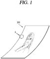
- FIG. 1 is a conceptual view showing a display device using a semiconductor light emitting element according to an embodiment of the present disclosure.
- information processed in the controller of the display device 100 may be displayed using a flexible display.
- the flexible display may include a flexible, bendable, twistable, foldable and rollable display.
- the flexible display may be a display fabricated on a thin and flexible substrate that can be warped, bent, folded or rolled like a paper sheet while maintaining the display characteristics of a flat display in the related art.
- a display area of the flexible display becomes a plane in a configuration that the flexible display is not warped (for example, a configuration having an infinite radius of curvature, hereinafter, referred to as a "first configuration”).
- the display area thereof becomes a curved surface in a configuration that the flexible display is warped by an external force in the first configuration (for example, a configuration having a finite radius of curvature, hereinafter, referred to as a "second configuration").
- information displayed in the second configuration may be visual information displayed on a curved surface.
- the visual information may be realized in such a manner that a light emission of each unit pixel (sub-pixel) arranged in a matrix configuration is controlled independently.
- the unit pixel denotes an elementary unit for representing one color.
- the sub-pixel of the flexible display may be implemented by a semiconductor light emitting element.
- a light emitting diode LED
- the light emitting diode may be formed with a small size to perform the role of a sub-pixel even in the second configuration through this.
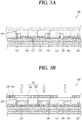
- FIG. 2 is a partial enlarged view of portion "A" in FIG. 1
- FIGS. 3A and 3B are cross-sectional views taken along lines B-B and C-C in FIG. 2
- FIG. 4 is a conceptual view illustrating a flip-chip type semiconductor light emitting element in FIG. 3A
- FIGS. 5A through 5C are conceptual views illustrating various forms for implementing colors in connection with a flip-chip type semiconductor light emitting element.
- FIGS. 2 , 3A and 3B there is illustrated a display device 100 using a passive matrix (PM) type semiconductor light emitting element as a display device 100 using a semiconductor light emitting element.
- PM passive matrix
- AM active matrix
- the display device 100 may include a substrate 110, a first electrode 120, a conductive adhesive layer 130, a second electrode 140, and a plurality of semiconductor light emitting elements 150.
- the substrate 110 may be a flexible substrate.
- the substrate 110 may contain glass or polyimide (PI) to implement the flexible display device.
- PI polyimide
- any one such as polyethylene naphthalate (PEN), polyethylene terephthalate (PET) or the like may be used.
- the substrate 110 may be either one of transparent and non-transparent materials.
- the substrate 110 may be a wiring substrate disposed with the first electrode 120, and thus the first electrode 120 may be placed on the substrate 110.
- an insulating layer 160 may be disposed on the substrate 110 placed with the first electrode 120, and an auxiliary electrode 170 may be placed on the insulating layer 160.
- a configuration in which the insulating layer 160 is deposited on the substrate 110 may be a single wiring substrate. More specifically, the insulating layer 160 may be incorporated into the substrate 110 with an insulating and flexible material such as polyimide (PI), PET, PEN or the like to form a single wiring substrate.
- PI polyimide
- PET PET
- PEN PEN
- the auxiliary electrode 170 as an electrode for electrically connecting the first electrode 120 to the semiconductor light emitting element 150 is placed on the insulating layer 160, and disposed to correspond to the location of the first electrode 120.
- the auxiliary electrode 170 has a dot shape, and may be electrically connected to the first electrode 120 by means of an electrode hole 171 passing through the insulating layer 160.
- the electrode hole 171 may be formed by filling a conductive material in a via hole.
- the conductive adhesive layer 130 may be formed on one surface of the insulating layer 160, but the present disclosure may not be necessarily limited to this.
- the conductive adhesive layer 130 may perform the role of an insulating layer in the structure in which the conductive adhesive layer 130 is disposed on the substrate 110.
- the conductive adhesive layer 130 may be a layer having adhesiveness and conductivity, and to this end, a conductive material and an adhesive material may be mixed on the conductive adhesive layer 130. Furthermore, the conductive adhesive layer 130 may have flexibility, thereby allowing a flexible function in the display device.
- the conductive adhesive layer 130 may be an anisotropic conductive film (ACF), an anisotropic conductive paste, a solution containing conductive particles, and the like.
- ACF anisotropic conductive film
- the conductive adhesive layer 130 may allow electrical interconnection in the z-direction passing through the thickness thereof, but may be configured as a layer having electrical insulation in the horizontal x-y direction thereof. Accordingly, the conductive adhesive layer 130 may be referred to as a z-axis conductive layer (however, hereinafter referred to as a "conductive adhesive layer").
- the anisotropic conductive film is a film with a form in which an anisotropic conductive medium is mixed with an insulating base member, and thus when heat and pressure are applied thereto, only a specific portion thereof may have conductivity by means of the anisotropic conductive medium.
- heat and pressure are applied to the anisotropic conductive film, but other methods may be also available for the anisotropic conductive film to partially have conductivity. The methods may include applying only either one of heat and pressure thereto, UV curing, and the like.
- the anisotropic conductive medium may be conductive balls or particles.
- the anisotropic conductive film is a film with a form in which an anisotropic conductive medium is mixed with an insulating base member, and thus when heat and pressure are applied thereto, only a specific portion thereof may have conductivity by means of the conductive balls.
- the anisotropic conductive film may be in a state in which a core with a conductive material contains a plurality of particles coated by an insulating layer with a polymer material, and in this case, it may have conductivity by means of the core while breaking an insulating layer on a portion to which heat and pressure are applied.
- a core may be transformed to implement a layer having both surfaces to which objects contact in the thickness direction of the film.
- heat and pressure are applied to an anisotropic conductive film as a whole, and electrical connection in the z-axis direction is partially formed by a height difference from a mating object adhered by the use of the anisotropic conductive film.
- an anisotropic conductive film may be in a state containing a plurality of particles in which a conductive material is coated on insulating cores.
- a portion to which heat and pressure are applied may be converted (pressed and adhered) to a conductive material to have conductivity in the thickness direction of the film.
- it may be formed to have conductivity in the thickness direction of the film in which a conductive material passes through an insulating base member in the z-direction.
- the conductive material may have a pointed end portion.
- the anisotropic conductive film may be a fixed array anisotropic conductive film (ACF) configured with a form in which conductive balls are inserted into one surface of the insulating base member.
- ACF fixed array anisotropic conductive film
- the insulating base member is formed of an adhesive material, and the conductive balls are intensively disposed at a bottom portion of the insulating base member, and when heat and pressure are applied thereto, the base member is modified along with the conductive balls, thereby having conductivity in the vertical direction thereof.
- the anisotropic conductive film may be all allowed to have a form in which conductive balls are randomly mixed with an insulating base member or a form configured with a plurality of layers in which conductive balls are disposed at any one layer (double-ACF), and the like.
- the anisotropic conductive paste as a form coupled to a paste and conductive balls may be a paste in which conductive balls are mixed with an insulating and adhesive base material.
- a solution containing conductive particles may be a solution in a form containing conductive particles or nano particles.
- the second electrode 140 is located at the insulating layer 160 to be separated from the auxiliary electrode 170.
- the conductive adhesive layer 130 is disposed on the insulating layer 160 located with the auxiliary electrode 170 and second electrode 140.
- the semiconductor light emitting element 150 is electrically connected to the first electrode 120 and second electrode 140.
- the semiconductor light emitting element may be a flip chip type semiconductor light emitting element.
- the semiconductor light emitting element may include a p-type electrode 156, a p-type semiconductor layer 155 formed with the p-type electrode 156, an active layer 154 formed on the p-type semiconductor layer 155, an n-type semiconductor layer 153 formed on the active layer 154, and an n-type electrode 152 disposed to be separated from the p-type electrode 156 in the horizontal direction on the n-type semiconductor layer 153.
- the p-type electrode 156 may be electrically connected to the welding portion 179 by the conductive adhesive layer 130
- the n-type electrode 152 may be electrically connected to the second electrode 140.
- the auxiliary electrode 170 may be formed in an elongated manner in one direction to be electrically connected to a plurality of semiconductor light emitting elements 150.
- the left and right p-type electrodes of the semiconductor light emitting elements around the auxiliary electrode may be electrically connected to one auxiliary electrode.
- the semiconductor light emitting element 150 is pressed into the conductive adhesive layer 130, and through this, only a portion between the p-type electrode 156 and auxiliary electrode 170 of the semiconductor light emitting element 150 and a portion between the n-type electrode 152 and second electrode 140 of the semiconductor light emitting element 150 have conductivity, and the remaining portion does not have conductivity since there is no push-down of the semiconductor light emitting element.
- the conductive adhesive layer 130 may form an electrical connection as well as allow a mutual coupling between the semiconductor light emitting element 150 and the auxiliary electrode 170 and between the semiconductor light emitting element 150 and the second electrode 140.
- a plurality of semiconductor light emitting elements 150 constitute a light-emitting array, and a phosphor layer 180 is formed on the light-emitting array.
- the light emitting element array may include a plurality of semiconductor light emitting elements with different self-luminance values.
- Each of the semiconductor light emitting elements 150 constitutes a sub-pixel, and is electrically connected to the first electrode 120.
- the semiconductor light emitting elements are arranged in several rows, for instance, and each row of the semiconductor light emitting elements may be electrically connected to any one of the plurality of first electrodes.
- the semiconductor light emitting elements may be connected in a flip chip form, and thus semiconductor light emitting elements grown on a transparent dielectric substrate. Furthermore, the semiconductor light emitting elements may be nitride semiconductor light emitting elements, for instance.
- the semiconductor light emitting element 150 has an excellent luminance characteristic, and thus it may be possible to configure individual sub-pixels even with a small size thereof.
- a partition wall 190 may be formed between the semiconductor light emitting elements 150.
- the partition wall 190 may perform the role of dividing individual sub-pixels from one another, and be formed as an integral body with the conductive adhesive layer 130.
- a base member of the anisotropic conductive film may form the partition wall when the semiconductor light emitting element 150 is inserted into the anisotropic conductive film.
- the partition wall 190 may have reflective characteristics while at the same time increasing contrast with no additional black insulator.
- a reflective partition wall may be separately provided with the partition wall 190.
- the partition wall 190 may include a black or white insulator according to the purpose of the display device. It may have an effect of enhancing reflectivity when the partition wall of the while insulator is used, and increase contrast while at the same time having reflective characteristics.
- the phosphor layer 180 may be located at an outer surface of the semiconductor light emitting element 150.
- the semiconductor light emitting element 150 is a blue semiconductor light emitting element that emits blue (B) light, and the phosphor layer 180 performs the role of converting the blue (B) light into the color of a sub-pixel.
- the phosphor layer 180 may be a red phosphor layer 181 or green phosphor layer 182 constituting individual pixels.
- a red phosphor 181 capable of converting blue light into red (R) light may be deposited on the blue semiconductor light emitting element 151 at a position implementing a red sub-pixel
- a green phosphor 182 capable of converting blue light into green (G) light may be deposited on the blue semiconductor light emitting element 151 at a position implementing a green sub-pixel.
- the blue semiconductor light emitting element 151 may be solely used at a location implementing a blue sub-pixel.
- the red (R), green (G) and blue (B) sub-pixels may implement one pixel.
- one color phosphor may be deposited along each line of the first electrode 120. Accordingly, one line on the first electrode 120 may be an electrode controlling one color.
- red (R), green (B) and blue (B) may be sequentially disposed along the second electrode 140, thereby implementing sub-pixels.
- the present disclosure may not be necessarily limited to this, and the semiconductor light emitting element 150 may be combined with quantum dot (QD) instead of phosphor to implement sub-pixels such as red (R), green (G) and blue (B).
- QD quantum dot
- a black matrix 191 may be disposed between each phosphor layer to enhance contrast.
- the black matrix 191 can enhance the contrast of luminance.
- the present disclosure may not be necessarily limited to this, and another structure for implementing blue, red and green may be also applicable thereto.
- each of the semiconductor light emitting elements 150 may be implemented with a high-power light emitting element that emits various lights including blue in which gallium nitride (GaN) is mostly used, and indium (In) and or aluminum (Al) are added thereto.
- GaN gallium nitride
- Al aluminum
- the semiconductor light emitting element 150 may be red, green and blue semiconductor light emitting elements, respectively, to implement each sub-pixel.
- red, green and blue semiconductor light emitting elements R, G, B
- red, green and blue sub-pixels implement one pixel by means of the red, green and blue semiconductor light emitting elements, thereby implementing a full color display.
- the semiconductor light emitting element may have a white light emitting element (W) provided with a yellow phosphor layer for each element.
- a red phosphor layer 181, a green phosphor layer 182 and blue phosphor layer 183 may be provided on the white light emitting element (W) to implement a sub-pixel.
- a color filter repeated with red, green and blue on the white light emitting element (W) may be used to implement a sub-pixel.
- a red phosphor layer 181, a green phosphor layer 182 and blue phosphor layer 183 may be provided on a ultra violet light emitting element (UV).
- UV ultra violet light emitting element
- the semiconductor light emitting element can be used over the entire region up to ultra violet (UV) as well as visible light, and may be extended to a form of semiconductor light emitting element in which ultra violet (UV) can be used as an excitation source.
- the semiconductor light emitting element 150 is placed on the conductive adhesive layer 130 to configure a sub-pixel in the display device.
- the semiconductor light emitting element 150 may have excellent luminance characteristics, and thus it may be possible to configure individual sub-pixels even with a small size thereof.
- the size of the individual semiconductor light emitting element 150 may be less than 80 ⁇ m in the length of one side thereof, and formed with a rectangular or square shaped element. In case of a rectangular shaped element, the size thereof may be less than 20 x 80 ⁇ m.
- a square shaped semiconductor light emitting element 150 with a length of side of 10 ⁇ m is used for a sub-pixel, it will exhibit a sufficient brightness for implementing a display device. Accordingly, for example, in case of a rectangular pixel in which one side of a sub-pixel is 600 ⁇ m in size, and the remaining one side thereof is 300 ⁇ m, a relative distance between the semiconductor light emitting elements becomes sufficiently large. Accordingly, in this case, it may be possible to implement a flexible display device having a HD image quality.
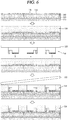
- a display device using the foregoing semiconductor light emitting element will be fabricated by a new type of fabrication method. Hereinafter, the fabrication method will be described with reference to FIG. 6 .
- FIG. 6 is cross-sectional views showing a fabrication method of a display device using a semiconductor light emitting element according to the present disclosure.
- the conductive adhesive layer 130 is formed on the insulating layer 160 located with the auxiliary electrode 170 and second electrode 140.
- the insulating layer 160 is deposited on the first substrate 110 to form one substrate (or wiring substrate), and the first electrode 120, auxiliary electrode 170 and second electrode 140 are disposed at the wiring substrate.
- the first electrode 120 and second electrode 140 may be disposed in a perpendicular direction to each other.
- the first substrate 110 and insulating layer 160 may contain glass or polyimide (PI), respectively, to implement a flexible display device.
- the conductive adhesive layer 130 may be implemented by an anisotropic conductive film, for example, and to this end, an anisotropic conductive film may be coated on a substrate located with the insulating layer 160.
- a second substrate 112 located with a plurality of semiconductor light emitting elements 150 corresponding to the location of the auxiliary electrodes 170 and second electrodes 140 and constituting individual pixels is disposed such that the semiconductor light emitting element 150 faces the auxiliary electrode 170 and second electrode 140.
- the second substrate 112 as a growth substrate for growing the semiconductor light emitting element 150 may be a sapphire substrate or silicon substrate.
- the semiconductor light emitting element may have a gap and size capable of implementing a display device when formed in the unit of wafer, and thus effectively used for a display device.
- the wiring substrate is thermally compressed to the second substrate 112.
- the wiring substrate and second substrate 112 may be thermally compressed to each other by applying an ACF press head.
- the wiring substrate and second substrate 112 are bonded to each other using the thermal compression. Only a portion between the semiconductor light emitting element 150 and the auxiliary electrode 170 and second electrode 140 may have conductivity due to the characteristics of an anisotropic conductive film having conductivity by thermal compression, thereby allowing the electrodes and semiconductor light emitting element 150 to be electrically connected to each other.
- the semiconductor light emitting element 150 may be inserted into the anisotropic conductive film, thereby forming a partition wall between the semiconductor light emitting elements 150.
- the second substrate 112 is removed.
- the second substrate 112 may be removed using a laser lift-off (LLO) or chemical lift-off (CLO) method.
- LLO laser lift-off
- CLO chemical lift-off
- the second substrate 112 is removed to expose the semiconductor light emitting elements 150 to the outside.
- Silicon oxide (SiOx) or the like may be coated on the wiring substrate coupled to the semiconductor light emitting element 150 to form a transparent insulating layer (not shown).
- the semiconductor light emitting element 150 may be a blue semiconductor light emitting element for emitting blue (B) light, and red or green phosphor for converting the blue (B) light into the color of the sub-pixel may form a layer on one surface of the blue semiconductor light emitting element.
- the fabrication method or structure of a display device using the foregoing semiconductor light emitting element may be modified in various forms.
- the foregoing display device may be applicable to a vertical semiconductor light emitting element.
- the vertical structure will be described with reference to FIGS. 5 and 6 .
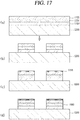
- FIG. 7 is a perspective view illustrating a display device using a semiconductor light emitting element according to another embodiment of the present disclosure.
- FIG. 8 is a cross-sectional view taken along line C-C in FIG. 7
- FIG. 9 is a conceptual view illustrating a vertical type semiconductor light emitting element in FIG. 8 .
- the display device may be display device using a passive matrix (PM) type of vertical semiconductor light emitting element.
- PM passive matrix
- the display device may include a substrate 210, a first electrode 220, a conductive adhesive layer 230, a second electrode 240 and a plurality of semiconductor light emitting elements 250.
- the substrate 210 as a wiring substrate disposed with the first electrode 220 may include polyimide (PI) to implement a flexible display device.
- PI polyimide
- any one may be used if it is an insulating and flexible material.
- the first electrode 220 may be located on the substrate 210, and formed with a bar-shaped electrode elongated in one direction.
- the first electrode 220 may be formed to perform the role of a data electrode.
- the conductive adhesive layer 230 is formed on the substrate 210 located with the first electrode 220. Similar to a display device to which a flip chip type light emitting element is applied, the conductive adhesive layer 230 may be an anisotropic conductive film (ACF), an anisotropic conductive paste, a solution containing conductive particles, and the like. However, the present embodiment illustrates a case where the conductive adhesive layer 230 is implemented by an anisotropic conductive film.
- ACF anisotropic conductive film
- the semiconductor light emitting element 250 When an anisotropic conductive film is located in a state that the first electrode 220 is located on the substrate 210, and then heat and pressure are applied to connect the semiconductor light emitting element 250 thereto, the semiconductor light emitting element 250 is electrically connected to the first electrode 220. At this time, the semiconductor light emitting element 250 may be preferably disposed on the first electrode 220.
- the electrical connection is generated because an anisotropic conductive film partially has conductivity in the thickness direction when heat and pressure are applied as described above. Accordingly, the anisotropic conductive film is partitioned into a portion 231 having conductivity and a portion 232 having no conductivity in the thickness direction thereof.
- anisotropic conductive film contains an adhesive component, and thus the conductive adhesive layer 230 implements a mechanical coupling as well as an electrical coupling between the semiconductor light emitting element 250 and the first electrode 220.
- the semiconductor light emitting element 250 is placed on the conductive adhesive layer 230, thereby configuring a separate sub-pixel in the display device.
- the semiconductor light emitting element 250 may have excellent luminance characteristics, and thus it may be possible to configure individual sub-pixels even with a small size thereof.
- the size of the individual semiconductor light emitting element 250 may be less than 80 ⁇ m in the length of one side thereof, and formed with a rectangular or square shaped element. In case of a rectangular shaped element, the size thereof may be less than 20 x 80 ⁇ m.
- the semiconductor light emitting element 250 may be a vertical structure.
- a plurality of second electrodes 240 disposed in a direction of crossing the length direction of the first electrode 220, and electrically connected to the vertical semiconductor light emitting element 250 may be located between vertical semiconductor light emitting elements.
- the vertical semiconductor light emitting element may include a p-type electrode 256, a p-type semiconductor layer 255 formed with the p-type electrode 256, an active layer 254 formed on the p-type semiconductor layer 255, an n-type semiconductor layer 253 formed on the active layer 254, and an n-type electrode 252 formed on the n-type semiconductor layer 253.
- the p-type electrode 256 located at the bottom thereof may be electrically connected to the first electrode 220 by the conductive adhesive layer 230
- the n-type electrode 252 located at the top thereof may be electrically connected to the second electrode 240 which will be described later.
- the electrodes may be disposed in the upward/downward direction in the vertical semiconductor light emitting element 250, thereby providing a great advantage capable of reducing the chip size.
- a phosphor layer 280 may be formed on one surface of the semiconductor light emitting element 250.
- the semiconductor light emitting element 250 is a blue semiconductor light emitting element 251 that emits blue (B) light
- the phosphor layer 280 for converting the blue (B) light into the color of the sub-pixel may be provided thereon.
- the phosphor layer 280 may be a red phosphor 281 and a green phosphor 282 constituting individual pixels.
- a red phosphor 281 capable of converting blue light into red (R) light may be deposited on the blue semiconductor light emitting element 251 at a position implementing a red sub-pixel
- a green phosphor 282 capable of converting blue light into green (G) light may be deposited on the blue semiconductor light emitting element 251 at a position implementing a green sub-pixel.
- the blue semiconductor light emitting element 251 may be solely used at a location implementing a blue sub-pixel. In this case, the red (R), green (G) and blue (B) sub-pixels may implement one pixel.
- the present disclosure may not be necessarily limited to this, and another structure for implementing blue, red and green may be also applicable thereto as described above in a display device to which a flip chip type light emitting element is applied.
- the second electrode 240 is located between the semiconductor light emitting elements 250, and electrically connected to the semiconductor light emitting elements 250.
- the semiconductor light emitting elements 250 may be disposed in a plurality of rows, and the second electrode 240 may be located between the rows of the semiconductor light emitting elements 250.
- the second electrode 240 may be located between the semiconductor light emitting elements 250.
- the second electrode 240 may be formed with a bar-shaped electrode elongated in one direction, and disposed in a perpendicular direction to the first electrode.
- the second electrode 240 may be electrically connected to the semiconductor light emitting element 250 by a connecting electrode protruded from the second electrode 240.
- the connecting electrode may be an n-type electrode of the semiconductor light emitting element 250.
- the n-type electrode is formed with an ohmic electrode for ohmic contact, and the second electrode covers at least part of the ohmic electrode by printing or deposition.
- the second electrode 240 may be electrically connected to the n-type electrode of the semiconductor light emitting element 250.
- the second electrode 240 may be located on the conductive adhesive layer 230.
- a transparent insulating layer (not shown) containing silicon oxide (SiOx) may be formed on the substrate 210 formed with the semiconductor light emitting element 250.
- SiOx silicon oxide
- the second electrode 240 may be located on the transparent insulating layer.
- the second electrode 240 may be formed to be separated from the conductive adhesive layer 230 or transparent insulating layer.
- a transparent electrode such as indium tin oxide (ITO) is used to locate the second electrode 240 on the semiconductor light emitting element 250
- the ITO material has a problem of bad adhesiveness with an n-type semiconductor. Accordingly, the second electrode 240 may be placed between the semiconductor light emitting elements 250, thereby obtaining an advantage in which the transparent electrode is not required. Accordingly, an n-type semiconductor layer and a conductive material having a good adhesiveness may be used as a horizontal electrode without being restricted by the selection of a transparent material, thereby enhancing the light extraction efficiency.
- a partition wall 290 may be formed between the semiconductor light emitting elements 250.
- the partition wall 290 may be disposed between the vertical semiconductor light emitting elements 250 to isolate the semiconductor light emitting element 250 constituting individual pixels.
- the partition wall 290 may perform the role of dividing individual sub-pixels from one another, and be formed as an integral body with the conductive adhesive layer 230.
- a base member of the anisotropic conductive film may form the partition wall when the semiconductor light emitting element 250 is inserted into the anisotropic conductive film.
- the partition wall 290 may have reflective characteristics while at the same time increasing contrast with no additional black insulator.
- a reflective partition wall may be separately provided with the partition wall 290.
- the partition wall 290 may include a black or white insulator according to the purpose of the display device.
- the partition wall 290 may be located between the semiconductor light emitting element 250 and second electrode 240. Accordingly, individual sub-pixels may be configured even with a small size using the semiconductor light emitting element 250, and a distance between the semiconductor light emitting elements 250 may be relatively sufficiently large to place the second electrode 240 between the semiconductor light emitting elements 250, thereby having the effect of implementing a flexible display device having a HD image quality.
- a black matrix 291 may be disposed between each phosphor layer to enhance contrast.
- the black matrix 291 can enhance the contrast of luminance.
- the semiconductor light emitting element 250 is located on the conductive adhesive layer 230, thereby constituting individual pixels on the display device.
- the semiconductor light emitting element 250 may have excellent luminance characteristics, and thus it may be possible to configure individual sub-pixels even with a small size thereof. As a result, it may be possible to implement a full color display in which the sub-pixels of red (R), green (G) and blue (B) implement one pixel by means of the semiconductor light emitting element.
- a semiconductor light emitting element grown on a wafer and formed through mesa and isolation is used as an individual pixel. Since a method of transferring a semiconductor light emitting element grown on a wafer to a wiring substrate is used, there is a problem that it is difficult to realize a large screen display due to a size limitation of the wafer. In order to solve such a problem, a method of assembling a semiconductor light emitting element into a wiring substrate in a self-assembly manner may be applied.
- the self-assembly method is a method of placing semiconductor light emitting elements on a wiring substrate or an assembly substrate in a chamber filled with a fluid.
- the semiconductor light emitting elements and the substrate are placed in a chamber filled with a fluid, and the fluid is heated in such a manner that the semiconductor light emitting elements are assembled to the substrate by themselves.
- the substrate may be provided with grooves into which the semiconductor light emitting elements are inserted. Specifically, grooves on which the semiconductor light emitting elements are placed at positions where the semiconductor light emitting elements are aligned with the wiring electrodes are formed on the substrate.
- the grooves are formed in a shape corresponding to a shape of the semiconductor light emitting elements, and the semiconductor light emitting elements are assembled into the grooves while randomly moving in the fluid.
- red semiconductor light emitting elements, green semiconductor light emitting elements, and blue semiconductor light emitting elements may be respectively self-assembled without using phosphors or color filters to enhance luminous efficiency.
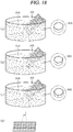
- FIG. 10 is an enlarged view of portion "A" in FIG. 1 for explaining another embodiment of the present disclosure to which a semiconductor light emitting element and a wiring substrate having a new structure are applied
- FIG. 11 is a cross-sectional view taken along line E-E in FIG. 10
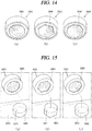
- FIGS. 12A , 12B and 12C are plan views illustrating the semiconductor light emitting elements in FIG. 10
- FIG. 13 is an enlarged view illustrating a semiconductor light emitting element in FIG. 10 .
- a display device 1000 using a semiconductor light emitting element is illustrated as a display device 1000 using a passive matrix (PM) type vertical semiconductor light emitting element.
- PM passive matrix
- AM active matrix
- the display device 1000 includes a substrate 1010, a first electrode 1020, a second electrode 1040, a plurality of semiconductor light emitting elements 1050, an insulating layer 1060, and metal pads 1070.
- the first electrode 1020 and the second electrode 1040 may respectively include a plurality of electrode lines.
- the substrate 1010 as a wiring substrate disposed with the first electrode 1020 may include polyimide (PI) to implement a flexible display device.
- PI polyimide
- any one may be used if it is an insulating and flexible material.
- the first electrode 1020 may be located on the substrate 1010, and formed with a bar-shaped electrode elongated in one direction.
- the first electrode 1020 may be formed to perform the role of a data electrode.
- an insulating layer 1060 may be disposed on the substrate 1010 placed with the first electrode 1020, and the metal pads 1070 may be placed on the insulating layer 1060. More specifically, the first electrode 1020 may be disposed on one surface of the substrate 1010, and the insulating layer 1060 covering the first electrode 1020 may be formed on the first surface 1020. In this case, a configuration in which the insulating layer 1060 is deposited on the substrate 1010 may be a single wiring substrate. In addition, the first electrode 1020 may be a lower wiring made of a conductive material.
- the insulating layer 1060 may be incorporated into the substrate 1010 with an insulating and flexible material such as polyimide (PI), PET, PEN or the like while covering the lower wiring to form a single wiring substrate.
- PI polyimide
- PET PET
- PEN insulating and flexible material
- the first electrode 1020 is a lower wiring electrode, which is bonded to a p-type electrode of the semiconductor light emitting element through a metal pad, and a main element at the top of the wiring electrode may be a single component of Au, Cu, In or Sn, or a mixed component having 2, 3 or 4 elements.
- the wiring electrode may have a thickness of 50 nm or more to reduce the resistance.
- the metal pads 1070 as an auxiliary electrode for electrically connecting the first electrode 1020 to the semiconductor light emitting element 1050 are placed on the insulating layer 1060, and disposed to correspond to the location of the first electrode 1020.
- the metal pads 1070 have a dot shape, and may be electrically connected to the first electrode 1020 by means of an insulating through hole 1071 passing through the insulating layer 1060.
- the metal pads 1070 may be connected to the lower wiring, and disposed to be exposed to an outside through the insulating layer 1060.
- the metal pads 1070 may be formed of a material having a low melting point and applied to the first electrode 1020 in a dot shape. More specifically, the metal pads 1070 are solder materials, and the first electrode 1020 and the semiconductor light emitting element 1050 are electrically and physically connected through soldering using the solder materials. Soldering refers to bonding metals together using solder, flux and heat.
- the solder material may be at least one of Sn, Ag, Cu, Pb, Al, Bi, Cd, Fe, In, Ni, Sb, Zn, Co and Au.
- the metal pad may be a metal alloy, and when the area of a GaN epi-layer is 100%, the area of the metal pad may be 25 to 100%, and an upper surface thereof may preferably have a circular shape, but may also have a polygonal shape with four or more sides.
- a height of the metal pad is 100 nanometers to 20 micrometers, and the height thereof may increase as the area increases.
- the metal pad has a convex shape protruded upward, and the component material may be a single component of In, Bi, Sn, Au, Cu or Ag, or a mixed component having 2, 3, 4, 5 or 6 elements.
- the semiconductor light emitting element 1050 has a shape sandwiched between the metal pads 1070 and includes a red semiconductor light emitting element 1051, a green semiconductor light emitting element 1052, and a blue semiconductor light emitting element 1053.
- the structures of the red semiconductor light emitting element 1051, the green semiconductor light emitting element 1052, and the blue semiconductor light emitting element 1053 are the same, and will be described first with reference to FIG. 13 .
- the structure of the semiconductor light emitting element described below may also be applicable to a case where a display device is formed using only one-color semiconductor light emitting elements, for example, blue semiconductor light emitting elements.
- the semiconductor light emitting element may be referred to as a micro-LED, has an area range of 25 to 250000 square micrometers, and a thickness of the chip may be about 2 to 10 micrometers.
- the semiconductor light emitting element 1050 includes a first conductive electrode 1156, a first conductive semiconductor layer 1155 formed with the first conductive electrode 1156, an active layer 1154 formed on the first conductive semiconductor layer 1155, a second conductive semiconductor layer 1153 formed on the active layer 1154, and a second conductive electrode 1152 formed on the second conductive semiconductor layer 1153.
- the first conductive semiconductor layer 1155 and the second conductive semiconductor layer 1153 overlap with each other, and the second conductive electrode 1152 is disposed on an upper surface of the second conductive semiconductor layer 1153, and the first conductive electrode 1156 is disposed on a lower surface of the first conductive semiconductor layer 1155.
- the upper surface of the second conductive semiconductor layer 1153 may be one surface of the second conductive semiconductor layer 1153 farthest from the first conductive semiconductor layer 1155
- the lower surface of the first conductive semiconductor layer 1155 may be one surface of the first conductive semiconductor layer 1155 farthest from the second conductive semiconductor layer 1153.
- the first conductive electrode 1156 and the second conductive electrode 1152 are respective disposed on the upper and lower sides of the first conductive semiconductor layer 1155 and the second conductive semiconductor layer 1153 by interposing them therebetween.
- the lower surface of the first conductive semiconductor layer 1155 may be a surface closest to the wiring substrate, and the upper surface of the second conductive semiconductor layer may be a surface farthest from the wiring substrate.
- first conductive electrode 1156 and the first conductive semiconductor layer 1155 may be a p-type electrode and a p-type semiconductor layer, respectively, and the second conductive electrode 1152 and the second conductive semiconductor layer 1153 may be an n-type electrode and an n-type semiconductor layer, respectively.
- first conductive type may be n-type and the second conductive type may be p-type.
- the p-type semiconductor layer may be p-type GaAs and the n-type semiconductor layer may be n-type GaAs.
- the p-type semiconductor layer may be p-type GaN and the n-type semiconductor layer may be n-type GaN.
- a p-electrode side in the p-type semiconductor layer in the present example may be p-type GaN doped with Mg, and an n-electrode side in the n-type semiconductor layer may be n-type GaN doped with Si.
- the above-described semiconductor light emitting elements may be semiconductor light emitting elements without an active layer.
- the semiconductor light emitting elements include an active layer, but a structure without an active layer in which a p-electrode side of the p-type semiconductor layer is P-type GaN doped with Mg and an n-electrode side of the n-type semiconductor layer is N-type GaN doped with Si.
- the conductive semiconductor layer may have an area range of 25 to 250000 square micrometers, and have a thickness of about 2 to 10 micrometers, and have a circular shape, but may also have a polygonal shape with five or more sides if necessary.
- the p-type electrode located at the top thereof may be electrically connected to the first electrode 1020 by the conductive adhesive layer 1030, and the n-type electrode 252 located at the bottom thereof may be electrically connected to the second electrode 1040.
- the p-type electrode may include a plurality of metal layers formed of different metals. For example, a plurality of metal layers made of Ti, Pt, Au, Ti, Cr or the like may be laminated to form the p-type electrode.
- the p-type electrode is bonded on Mg-doped GaN, and may be made of Au, Cu, or a mixture thereof.
- the area is 30 to 75% of the area of a GaN epi-layer, and the position of the electrode may be disposed at the center of the GaN epi-layer.
- the shape of the electrode may preferably have a circular shape, but may also have a polygonal shape with four or more sides if necessary.
- the area and shape of the p-type electrode refers only to a portion of the p-type electrode that is open without being covered by the passivation layer.
- a pure area of the p-type electrode is between a partial area of the p-type electrode that is off and a total area of the GaN epi-layer. Furthermore, in order to enhance a bonding strength between GaN and Au or Cu, a Ti, Cr, or Pt layer may be added to the interface. A total thickness of the p-type electrode may be between 100 nanometers and 5 micrometers.
- the semiconductor light emitting element includes a passivation layer 1160 formed to surround the lateral surfaces of the first conductive semiconductor layer 1155 and the second conductive semiconductor layer 1153.
- the passivation layer 1160 covers the lateral surface of the semiconductor light emitting element to stabilize the characteristics of the semiconductor light emitting element and is formed of an insulating material. As described above, the first conductive semiconductor layer 1155 and the second conductive semiconductor layer 1153 are electrically disconnected by the passivation layer 1160, and thus the p-type GaN and n-type GaN of the semiconductor light emitting element may be insulated from each other.
- the passivation layer 1160 includes a through hole 1161 to expose the first conductive electrode 1156.
- the metal pad 1070 is inserted into the through hole 1161, so that the semiconductor light emitting element can be coupled to the wiring substrate.
- the wiring substrate is immersed in a fluid in a state where the metal pad 1070 is melted, and the metal pad 1070 and the conductive electrodes are coupled to each other while the metal pad 1070 is solidified.
- a lower surface of the passivation layer 1160 may be protruded from a lower surface of the conductive electrode so as to restrict any one conductive electrode of the plurality of semiconductor light emitting elements from being in contact with another conductive electrode thereof during self-assembly.
- it may have a structure in which the passivation layer 1160 covers a lower surface of the first conductive electrode 1156 (the farthest surface from the conductive semiconductor layer), and the first conductive electrode 1156 does not pass through the through hole 1161.
- the first conductive electrode 1156 is covered in a concave shape by the passivation layer 1160, and the metal pad 1070 is coupled to the first conductive electrode 1156 through the through hole 1161.
- the material of the passivation layer 1160 may be SiO 2 or SiNx, covering all of the sides of the GaN epi-layer and exposing the central portion of the conductive electrode.
- the lower surface is formed to cover all portions of the p-type electrode or the GaN epi-layer except for a portion of the p-type electrode exposed to the outside.
- the passivation becomes 70% when an area of the p-type electrode that is open at the center occupies 30%, and the passivation becomes 25% when an area of the p-type electrode that is open at the center occupies 75%.
- an area of the passivation layer below the chip may be a 100-open p-type electrode area when an area of the GaN epi-layer is 100.
- a thickness of the passivation layer is 50 nanometers to 5 micrometers, and a thickness covering a lower surface thereof and a thickness covering a side surface thereof may be different from each other.
- each of the light emitting elements 1051, 1052, 1053 may include an identification portion 1080.
- the red semiconductor light emitting element 1051, the green semiconductor light emitting element 1052, and the blue semiconductor light emitting element 1053 may be distinguished from each other using the identification portion 1080, and through this, it may be easily checked whether the assembled state is normal after each chip is selectively self-assembled.
- a structure in which different colors identify semiconductor light emitting elements using identification portions but the present disclosure is not necessarily limited thereto.
- a concave structure of the above-described semiconductor light emitting element, a structure in which the metal pad is inserted into the through hole, and the like may be used singly regardless of the identification portion described below.
- the identification portion 1080 is formed to have different shapes according to the color of emitted light to distinguish the semiconductor light emitting elements in a state where the semiconductor light emitting elements are coupled to the substrate.
- the identification portion 1080 may be formed on any one of the conductive semiconductor layers 1153, 1155, the conductive electrode 1156, and the passivation layer 1160.
- the identification portion 1080 may be the conductive semiconductor layers 1153, 1155.
- the shapes of a conductive semiconductor layer of the red semiconductor light emitting element 1051 (hereinafter, referred to as a red conductive semiconductor layer), a conductive semiconductor layer of the green semiconductor light emitting element 1052 (hereinafter, referred to as a green conductive semiconductor layer), and a conductive semiconductor layer of the blue semiconductor light emitting element 1051 (hereinafter, referred to as a blue conductive semiconductor layer) may be different from each other.
- the conductive semiconductor layer forming the identification portion 1080 may be at least one of a first conductive semiconductor layer 1153 and a second conductive semiconductor layer 1155.
- any one of the red conductive semiconductor layer, the green conductive semiconductor layer, and the blue conductive semiconductor layer may have a cylindrical shape, and the remaining two may have a shape partially deformed from the cylindrical shape while having a symmetrical structure.
- the red conductive semiconductor layer has a cylindrical shape according to FIG. 12A
- the green conductive semiconductor layer has a hexagonal columnar shape according to FIG. 12B
- the blue conductive semiconductor layer has an octagonal columnar shape according to FIG. 12C .
- the planar shape of the red conductive semiconductor layer may be circular
- the planar shape of the green conductive semiconductor layer may be hexagonal
- the planar shape of the blue conductive semiconductor layer may be octagonal.
- the identification portion 1080 may have different shapes of the conductive semiconductor layers 1153, 1155.
- the shape of the conductive semiconductor layers 1153, 1155 may be an overall shape of the semiconductor light emitting element, and accordingly, the identification portion 1080 may have different shapes of the semiconductor light emitting elements.
- the different shapes may include a circle, a rectangle, a pentagon, a hexagon, an octagon, and the like.
- the red conductive semiconductor layer, the green conductive semiconductor layer, and the blue conductive semiconductor layer may be formed in different sizes. Since the shape of the conductive semiconductor layers 1153, 1155 is an overall shape of the semiconductor light emitting element as described above, the identification portion 1080 may have different sizes of the red semiconductor light emitting element 1051, the green semiconductor light emitting element 1052, and the blue semiconductor light emitting element 1053.
- the identification portion 1080 may be formed of a combination of the shapes and sizes of the red conductive semiconductor layer, the green conductive semiconductor layer, and the blue conductive semiconductor layer.
- any one of the shapes of the red conductive semiconductor layer, the green conductive semiconductor layer, and the blue conductive semiconductor layer is different from another one in shape, and the size thereof may be different from the remaining one.
- the red conductive semiconductor layer may have a large circular shape
- the green conductive semiconductor layer may have a small circular shape
- the blue conductive semiconductor layer may have a hexagonal shape.
- the red semiconductor light emitting element, the green semiconductor light emitting element, and the blue semiconductor light emitting element may be visually distinguished from each other.
- the red semiconductor light emitting element 1051 may be replaced with the green semiconductor light emitting element 1052 or the blue semiconductor light emitting element 1053.
- two blue semiconductor light emitting elements 1053 and one green semiconductor light emitting element 1052 may form one pixel in the semiconductor light emitting elements, an in this case, one of the blue semiconductor light emitting elements 1053 may form a blue sub-pixel, and the other one may form a red sub-pixel.
- a phosphor layer may overlap with an upper surface of the blue semiconductor light emitting element 1053.
- the phosphor layer performs a function of converting the blue light into a color of a unit pixel.
- the phosphor layer includes a red phosphor and converts blue light of the blue semiconductor light emitting element into red light in a red sub-pixel.
- a red color filter (not shown) for filtering a wavelength range other than light corresponding to red light overlaps with an upper surface of the phosphor layer to improve color purity.
- the identification portion 1080 is provided only for the green semiconductor light emitting element 1052 and the blue semiconductor light emitting element 1053. Moreover, even in another embodiment of the present disclosure described later with reference to FIGS. 14 through 16 , the blue semiconductor light emitting element 1053 may be provided for a red sub-pixel, and in this case, the identification portion 1080 may be formed only for the green semiconductor light emitting element 1052 and the blue semiconductor light-emitting element 1053.
- a plurality of second electrodes 1040 disposed in a direction of crossing the length direction of the first electrode 1020, and electrically connected to the semiconductor light emitting element 1050 may be located between the semiconductor light emitting elements.
- the second electrode 1040 may be located on a planarizing layer 1030.
- the planarizing layer 1030 is disposed between the insulating layer 1060 and the second electrode 1040 of the wiring substrate. More specifically, an insulating material is filled between the semiconductor light emitting elements to form a planarizing layer, and the second electrode 1040, which is an upper wiring, is disposed on one surface of a planarizing layer 1030.
- the second electrode 1040 may be electrically connected by contact with the second conductive electrode 1040 of the semiconductor light emitting element 1050.
- a plurality of semiconductor light emitting elements 1050 are coupled to the wiring substrate 1010, and electrically connected to the first electrode 1020 and the second electrode 1040 by the foregoing structure.
- the plurality of semiconductor light emitting elements 1050 may form a plurality of rows in a direction parallel to a plurality of electrode lines provided in the first electrode 1020.
- the present disclosure is not necessarily limited thereto.
- the plurality of semiconductor light emitting elements 1050 may form a plurality of rows along the second electrode 1040.
- the semiconductor light emitting element and the metal pad of the present example are provided with a mechanism capable of ensuring assembly reliability during self-assembly.
- the metal pads 1070 may include a first metal solder 1071 electrically connected to the conductive electrode 1156 of the green semiconductor light emitting element and a second metal solder 1072 electrically connected to the conductive electrode 1156 of the blue semiconductor light emitting element.
- the first metal solder 1071 and the second metal solder 1072 may be formed of materials having different melting points.
- the metal pad may include a third metal solder 1073 electrically connected to the conductive electrode 1156 of the red semiconductor light emitting element 1051, and the third metal solder 1073 may be formed of a material having a melting point different from that of at least one of the first metal solder 1071 and the second metal solder 1072.
- the first metal solder 1071, the second metal solder 1072, and the third metal solder 1073 may be solder materials having melting points from a high temperature to a low temperature in a self-assembly sequence. If the order of self-assembly is in the sequence of the red semiconductor light emitting element 1051, the green semiconductor light emitting element 1052, and the blue semiconductor light emitting element 1053, then the metal solders thereof may be formed of materials having high melting points in the sequence of the corresponding metal solders. In other words, if the semiconductor light emitting element that is self-assembled first is the green semiconductor light emitting element 1052, the second metal solder 1072 is formed of a material having the highest melting point.
- the melting point is controlled by adjusting one or more elements among the metals of Sn, Ag, Cu, Pb, Al, Bi, Cd, Fe, In, Ni, Sb, Zn, Co and Au or an 8-component composition.
- the components of the metals may be suitably adjusted to have a melting point temperature between 45 and 300 °C, and for a more specific example, a metal solder between 150 and 300 °C capable of withstanding the driving conditions of a display and the post-process temperature thereof may be used.
- FIGS. 14 through 16 are conceptual views showing various forms of implementing an identification portion with respect to the semiconductor light emitting element.
- the identification portion 2080 is a conductive electrode of the green semiconductor light emitting element 2052 and a conductive electrode of the blue semiconductor light emitting element 2053, and the conductive electrode of the green semiconductor light emitting element 2052 and the conductive electrode of the blue semiconductor light emitting element 2053 may have different shapes and sizes.
- the identification portions 2080 which are a first conductive electrode (hereinafter, referred to as a green conductive electrode) of the green semiconductor light emitting element 2052 shown in (b) of FIG. 14 and a second conductive electrode (hereinafter, referred to as a blue conductive electrode) of the blue semiconductor light emitting element 2053 shown in (c) of FIG. 14 , may have different shapes and sizes.
- the first conductive electrode (hereinafter, referred to as a red conductive electrode) of the red semiconductor light emitting element 2051 shown in (a) of FIG. 14 may have a different shape or size from the green conductive electrode and the blue conductive electrode.
- the red conductive electrode may be circular
- the green conductive electrode may be hexagonal
- the blue conductive electrode may be octagonal.
- the sizes of the electrodes may increase in the order of the red conductive electrode, the green conductive electrode, and the blue conductive electrode.
- the shapes of the red conductive electrode, the green conductive electrode, and the blue conductive electrode may be visually distinguished from each other. Therefore, according to the structure of this example, it may be determined by visual inspection whether the red semiconductor light emitting element, the green semiconductor light emitting element, and the blue semiconductor light emitting element are self-assembled at preset positions.
- FIG. 15 the same reference numerals are designated to the same components as those of the example described above with reference to FIGS. 10 through 13 , and the description thereof will be substituted by the earlier description. Specifically, the remaining configurations except for the identification portion 3080 and the metal pad are the same as those of the example described in FIGS. 10 through 13 .
- the identification part 3080 is a passivation layer of the green semiconductor light emitting element 3052 shown in (b) of FIG. 15 and a passivation layer of the blue semiconductor light emitting element 3053 shown in (c) of FIG. 15 , and a through hole (hereinafter, referred to as a green through hole) formed in the passivation layer of the green semiconductor light emitting element 3052 and a through hole (hereinafter, referred to as a green through hole) formed in the passivation layer of the blue semiconductor light emitting element 3053 may have different shapes and sizes.
- a through hole (hereinafter, referred to as a red through hole) formed in the passivation layer of the red semiconductor light emitting element 3051 may have a different shape or size from that of the green through hole and the blue through hole.
- the red through hole may be circular
- the green through hole may be hexagonal
- the blue through hole may be octagonal.
- the sizes of the through holes may increase in the order of the red through hole, the green through hole, and the blue through hole.
- the shapes of the through holes are formed to be different from each other, it may be defined that the shapes of the passivation layers are formed to be different from each other in this example.
- a first portion 3072 to which a conductive electrode of the green semiconductor light emitting element is coupled, and a second portion 3073 to which a conductive electrode of the blue semiconductor light emitting element may have different shapes or sizes.
- a third portion 3071 to which a conductive electrode of the red semiconductor light emitting element is coupled may have a different shape or size from that of the first portion 3072 and the second portion 3073.
- the through holes corresponding to the red semiconductor light emitting element 3051, the green semiconductor light emitting element 3052, and the blue semiconductor light emitting element 3053 may be formed to have different shapes or sizes.
- the insulating through holes may be formed to have the same shape as the through holes of the corresponding semiconductor light emitting elements, respectively.
- the first insulating through hole 3062 corresponding to the green through hole may be hexagonal
- the second insulating through hole 3063 corresponding to the blue through hole may be octagonal
- the third insulating through hole 3061 corresponding to the red through hole may be circular.
- first portion 3072, the second portion 3073 and the third portion 3071 may be solder coated through hexagonal, octagonal and circular through holes, respectively, and thus the first portion 3072, the second portion 3073 and the third portion 3071 may be more easily inserted into the corresponding passivation.
- FIG.18 it is illustrated a display device using passive matrix (PM) flip-chip type semiconductor light emitting elements as a display device 1000 using semiconductor light emitting elements.
- PM passive matrix
- AM active matrix
- the semiconductor light emitting element 4050 may be a circular, triangular, square and polygonal shape having symmetry.
- a circular semiconductor light emitting element 4050 will be described as an example.
- the semiconductor light emitting element includes a first conductive electrode 4156, a first conductive semiconductor layer 4155 formed with the first conductive electrode 4156, an active layer 4154 formed on the first conductive semiconductor layer 4155, a second conductive semiconductor layer 4153 formed on the active layer 4154, and a second conductive electrode 4152 formed on the second conductive semiconductor layer 4153.
- a lower surface of the first conductive semiconductor layer 4155 may be a surface closest to the substrate 4010, and an upper surface of the second conductive semiconductor layer 4153 may be a surface the farthest from the substrate 4010.
- first and second conductive electrodes 4156, 4152 are disposed on the lower surfaces of the first conductive semiconductor layer 4155 and the second conductive semiconductor layer 4153, respectively, and the first conductive electrode 4156 and the second conductive electrode 4152 may be arranged to be spaced apart from each other in a horizontal direction.
- the semiconductor light emitting element according to the present disclosure further includes a passivation layer 4160 formed to surround the semiconductor light emitting element.
- the passivation layer 4160 may be disposed between the first conductive electrode 4156 and the second conductive electrode 4152, and the first conductive electrode 4156 and the second conductive electrode 4152 may be insulated from each other through the passivation layer 4160.
- the passivation layer 4160 is formed to surround at least part of the side surfaces of the first conductive semiconductor layer 4155, the active layer 4154 and the second conductive semiconductor layer 4153.
- the passivation layer 4160 may have an annular first through hole 4161 and a circular second through hole 4162.
- the first through hole 4161 may be formed to surround the second through hole 4162.
- the first conductive semiconductor layer 4155 is exposed to the outside through the first through hole 4161, and the second conductive semiconductor layer 4156 is formed on the first conductive semiconductor layer 4155 exposed through the first through hole 4161.
- the second conductive semiconductor layer 4153 is exposed to the outside through the second through hole 4162, and the second conductive electrode 4152 is formed on one surface of the second conductive semiconductor layer 4153 exposed through the second through hole 4162.
- the first conductive electrode 4156 is extended along an outer circumference of the second through hole 4162 to surround the second conductive electrode 4152 as shown in the illustration.
- the first conductive electrode 4156 may have an annular shape.
- the first electrode 4020 and the second electrode 4040 may be formed on different layers of the substrate, and may have a structure in which part of the substrate is exposed to the outside.
- a solder material may be applied to each of the first electrode 4020 and the second electrode 4040, and coupled to the first conductive electrode 4156 and the second conductive electrode 4152.
- first conductive electrode 4156 and the first conductive semiconductor layer 4155 may be a p-type electrode and a p-type semiconductor layer, respectively, and the second conductive electrode 4152 and the second conductive semiconductor layer 4153 may be an n-type electrode and an n-type semiconductor layer, respectively.
- an undoped semiconductor layer 4153a may be formed on the other surface of the second conductive semiconductor layer 4153.
- the identification portion 4080 may be grooves formed in the undoped semiconductor layer.
- grooves are formed in the undoped semiconductor layer of the green semiconductor light emitting element 4052 and the undoped semiconductor layer of the blue semiconductor light emitting element 4053, and patterns formed by the grooves may be different from each other on the green semiconductor light emitting element 4052 and the blue semiconductor light emitting element 4053. Moreover, grooves having a different pattern from those of the undoped semiconductor layers of the green semiconductor light emitting element 4052 and the blue semiconductor light emitting element 4053 may be formed on the undoped semiconductor layer of the red semiconductor light emitting element 4051.
- the grooves may be a pattern implemented by texturing, and the pattern may vary depending on the color of light emitted from the semiconductor light emitting element, thereby allowing visual inspection.
- a display device in which the semiconductor light emitting elements are sequentially self-assembled according to their colors may be implemented, and a structure capable of inspecting the assembled state during self-assembly may be implemented.
- FIGS. 17 and 18 are conceptual views showing a method of manufacturing a display device according to the present disclosure.
- a second conductive semiconductor layer 1153, an active layer 1154, and a first conductive semiconductor layer 1155 are respectively grown on a growth substrate 1200 (wafer) ((a) of FIG. 17 ).
- the active layer 1154 is grown on the second conductive semiconductor layer 1153, and then the first conductive semiconductor layer 1155 is grown on the active layer 1154.
- the growth substrate 1200 may be formed of any one of materials having light transmission properties, for example, sapphire (Al 2 O 3 ), GaN, ZnO, and AlO, but is not limited thereto. Furthermore, the growth substrate 1200 may be formed of a carrier wafer, which is a material suitable for semiconductor material growth. The growth substrate 1200 may be formed of a material having an excellent thermal conductivity, and for example, a SiC substrate having a higher thermal conductivity than a sapphire (Al 2 O 3 ) substrate or a SiC substrate including at least one of Si, GaAs, GaP, InP and Ga 2 O 3 may be used.
- isolation is carried out such that a plurality of light emitting elements form a light emitting element array on the growth substrate 1200.
- the first conductive semiconductor layer 1155, the active layer 1154, and the second conductive semiconductor layer 1153 are etched to form a plurality of semiconductor light emitting elements ((b) of FIG. 17 ).
- the first conductive electrode 1156 is formed on the first conductive semiconductor layer 1155 exposed to the outside as illustrated in (c) of FIG. 17 , and the passivation layer 1160 formed to surround the semiconductor light emitting element is formed as illustrated in (d) of FIG. 17 .
- the green semiconductor light emitting element and the blue semiconductor light emitting element may be separately grown on the growth substrate so that the light emitting structure of the green semiconductor light emitting element and the blue semiconductor light emitting element is grown.
- the red semiconductor light emitting element may be grown on a separate growth substrate so that the light emitting structure of the red semiconductor light emitting element is grown.
- the semiconductor light emitting elements may include identification portions, and the identification portions are configured to have different shapes according to the color of emitted light to be distinguished in a state where the semiconductor light emitting elements are coupled to the substrate.
- the identification portion may be formed in any one of the conductive semiconductor layer, the conductive electrode, and the passivation layer.
- the above-described identification portion is provided in the conductive semiconductor layer with reference to FIGS. 10 to 13 .
- FIG. Accordingly, the plane shape of a red conductive semiconductor layer is circular, the plane shape of a green conductive semiconductor layer is hexagonal, and the plane shape of a blue conductive semiconductor layer may be octagonal.
- this embodiment is not limited thereto, and it is also possible to provide the identification portion in another embodiment described above with reference to FIGS. 14 through 16 .
- the green semiconductor light emitting elements 1052 and the blue semiconductor light emitting elements 1053 are separated from the growth substrate, and sequentially coupled to the substrate 1010 through self-assembly in a chamber filled with a fluid.
- the red semiconductor light emitting elements 1051 may also be separated from the growth substrate and coupled to the substrate 1010 through self-assembly.
- the red semiconductor light emitting elements 1051 and the substrate 1010 are first placed in a chamber filled with a fluid, and the red semiconductor light emitting elements 1051 are self-assembled to the substrate 1010 by heating the fluid.
- metal solder may be applied to the substrate 1010 only at positions where the red semiconductor light emitting elements 1051 are to be assembled.
- a lower surface of the passivation layer 1160 of the semiconductor light emitting element may be protruded from a lower surface of the conductive electrode.
- it may have a structure in which the passivation layer 1160 covers a lower surface of the first conductive electrode 1156 (the farthest surface from the conductive semiconductor layer), and the first conductive electrode 1156 does not pass through the through hole 1161.
- the first conductive electrode 1156 may be covered in a concave shape by the passivation layer 1160, and therefore, the conductive electrodes of adjacent semiconductor light emitting elements may be alleviated and prevented from being in contact with each other.
- such a concave structure is not limited to this example, and may also be applicable to, for example, a case where one-color semiconductor light emitting elements are self-assembled.
- the green semiconductor light emitting elements 1052 and the substrate 1010 are placed in the chamber to induce the self-assembly of the green semiconductor light emitting elements 1052 by heating the fluid.
- metal solder may be applied to the first electrode on the substrate 1010 at positions where the green semiconductor light emitting elements 1052 are to be assembled.
- the metal solder at this time may be formed of a material having a melting point lower than that of the metal solder at positions where the red semiconductor light emitting elements 1051 are assembled.
- the blue semiconductor light emitting elements 1053 and the substrate 1010 are placed in the chamber to induce the self-assembly of the blue semiconductor light emitting elements 1053 by heating the fluid.
- metal solder having a melting point lower than that of red and green may be applied to the substrate 1010 at positions where the blue semiconductor light emitting elements 1053 are to be assembled.
- the metal solders may be solder materials having melting points from a high temperature to a low temperature in a self-assembly sequence.
- the process of inspecting whether the green semiconductor light emitting elements 1051 and the blue semiconductor light emitting elements 1053 are coupled to the preset positions of the substrate 1010 is carried out. Furthermore, when the red semiconductor light emitting elements 1051 are self-assembled together with the green semiconductor light emitting elements 1052 and the blue semiconductor light emitting elements 1053, it may also be inspected whether the red semiconductor light emitting elements 1051 are coupled to the preset positions of the substrate 1010.
- the inspection may be carried out through identification portions having different shapes so as to be distinguished in a state where the semiconductor light emitting elements are coupled to the substrate.
- the inspection may be carried out after all the red semiconductor light emitting elements, the green semiconductor light emitting elements, and the blue semiconductor light emitting elements are self-assembled, but the present disclosure is not limited thereto.
- the inspection may be carried out subsequent to the self-assembly process of the red semiconductor light emitting elements 1051, the green semiconductor light emitting elements 1052, and the blue semiconductor light emitting elements 1053.
- the semiconductor light emitting elements assembled at other positions other than the preset positions among the semiconductor light emitting elements may be removed by the inspection.
- the semiconductor light emitting element that emits light of a color corresponding to the removed vacant space may be self-assembled again, and then the remaining processes such as forming a planarizing layer, and depositing the second electrode may be carried out to implement a display device.
Landscapes
- Engineering & Computer Science (AREA)
- Microelectronics & Electronic Packaging (AREA)
- Power Engineering (AREA)
- Computer Hardware Design (AREA)
- Manufacturing & Machinery (AREA)
- Physics & Mathematics (AREA)
- Condensed Matter Physics & Semiconductors (AREA)
- General Physics & Mathematics (AREA)
- Optics & Photonics (AREA)
- Led Device Packages (AREA)
- Devices For Indicating Variable Information By Combining Individual Elements (AREA)
Abstract
Description
- The present disclosure relates to a display device and a fabrication method thereof, and more particularly, to a flexible display device using a semiconductor light emitting element.
- In recent years, display devices having excellent characteristics such as low profile, flexibility and the like have been developed in the display technical field. On the contrary, currently commercialized main displays are represented by liquid crystal displays (LCDs) and active matrix organic light emitting diodes (AMOLEDs).
- However, there exist problems such as not-so-fast response time, difficult implementation of flexibility in case of LCDs, and there exist drawbacks such as short life span, not-so-good yield as well as low flexibility in case of AMOLEDs.
- On the other hand, light emitting diodes (LEDs) are well known semiconductor light emitting elements for converting an electrical current to light, and have been used as a light source for displaying an image in an electronic device including information communication devices since red LEDs using GaAsP compound semiconductors were made commercially available in 1962, together with a GaP:N-based green LEDs. Accordingly, the semiconductor light emitting elements may be used to implement a flexible display, thereby presenting a scheme for solving the problems.
- As described above, in case of a display using semiconductor light emitting elements, it is difficult to implement a large-sized display device. Therefore, in recent years, a manufacturing method in which semiconductor light emitting elements are coupled to a substrate in a self-assembly manner has been developed. Further, in case of a display using semiconductor light emitting elements, a method of implementing red, green and blue colors by combining a blue semiconductor light emitting element with a phosphor, a color filter and the like is widely used, but such a structure has a disadvantage of low luminous efficiency.
- Accordingly, a mechanism for coupling a red semiconductor light emitting element, a green semiconductor light emitting element, and a blue semiconductor light emitting element, respectively, to the substrate through self-assembly may be taken into consideration.
- An aspect of the present disclosure is to provide a structure capable of inspecting an assembled state of semiconductor light emitting elements during self-assembly in a display device.
- Another aspect of the present disclosure is to provide a display device capable of sequentially self-assembling red semiconductor light emitting elements, green semiconductor light emitting elements, and blue semiconductor light emitting elements, and a manufacturing method thereof.
- In a display device using semiconductor light emitting elements, red semiconductor light emitting elements, green semiconductor light emitting elements, and blue semiconductor light emitting elements may be visually distinguished from each other, and the assembled state of the semiconductor light emitting elements during self-assembly may be easily inspected.
- Specifically, a display device according to the present disclosure may include a substrate having a plurality of metal pads, and green semiconductor light emitting elements and blue semiconductor light emitting elements electrically connected to the metal pads through self-assembly, wherein the green semiconductor light emitting elements and the blue semiconductor light emitting elements have identification portions having different shapes to be distinguished while being coupled to the substrate.
- According to an embodiment, the green semiconductor light emitting elements and the blue semiconductor light emitting elements respectively may include a conductive semiconductor layer, a conductive electrode formed on one surface of the conductive semiconductor layer, and a passivation layer configured to surround the semiconductor light emitting element, and provided with a through hole through which the conductive electrode is exposed, wherein the identification portion is formed on any one of the conductive semiconductor layer, the conductive electrode, and the passivation layer.
- According to an embodiment, the display device may further include a red semiconductor light emitting element electrically connected to the metal pads through self-assembly. Any one of a conductive semiconductor layer, a conductive electrode, and a passivation layer of the red semiconductor light emitting element may have a different shape or size from that of the green semiconductor light emitting element and the blue semiconductor light emitting element.
- According to an embodiment, the metal pad may include first metal solder electrically connected to a conductive electrode of the green semiconductor light emitting element and second metal solder electrically connected to a conductive electrode of the blue semiconductor light emitting element. The first metal solder and the second metal solder may be formed of materials having different melting points.
- According to an embodiment, the green semiconductor light emitting element and the blue semiconductor light emitting element may respectively include an undoped semiconductor layer, and the identification portion is formed on the undoped semiconductor layer. Grooves may be formed in the undoped semiconductor layer of the green semiconductor light emitting element and the undoped semiconductor layer of the blue semiconductor light emitting element, and patterns formed with the grooves may be configured to be different in the green semiconductor light emitting element and the blue semiconductor light emitting element.
- According to an embodiment, the green semiconductor light emitting element and the blue semiconductor light emitting element may have different shapes, and the identification portions may have the different shapes.
- In addition, the present disclosure discloses a method of manufacturing a display device, and the method may include growing green semiconductor light emitting elements and blue semiconductor light emitting elements separately on a growth substrate to grow light emitting structures of the green semiconductor light emitting elements and the blue semiconductor light emitting elements, separating the green semiconductor light emitting elements and the blue semiconductor light emitting elements from the growth substrate, and sequentially coupling them to a substrate through self-assembly in a chamber filled with a fluid, and inspecting whether the green semiconductor light emitting elements and the blue semiconductor light emitting elements are coupled to the preset positions of the substrate, wherein the green semiconductor light emitting elements and the blue semiconductor light emitting elements have identification portions having different shapes to be distinguished while being coupled to the substrate.
- According to an embodiment, solder materials for bonding semiconductor light emitting elements and wiring electrodes may be set to have melting points from a high temperature to a low temperature in a self-assembly sequence of the semiconductor light emitting elements.
- In a display device according to the present disclosure, red semiconductor light emitting elements, green semiconductor light emitting elements, and blue semiconductor light emitting elements may be sequentially self-assembled using solder materials having melting points from a high temperature to a low temperature in a self-assembly sequence. Through this, the present disclosure may realize a large-screen display with high luminous efficiency.
- Furthermore, according to the present disclosure red semiconductor light emitting elements, green semiconductor light emitting elements, and blue semiconductor light emitting elements may be distinguished using an identification portion, thereby easily checking whether the assembled state is normal after each chip is selectively self-assembled. As described above, the assembled state may be visually inspected without applying power while semiconductor light emitting elements are coupled to a substrate, and thus a repair process may be carried out immediately after the semiconductor light emitting elements are coupled to the substrate. Therefore, the repair process may be more easily carried out prior to performing the post-process, thereby further facilitating repair.
- The accompanying drawings, which are included to provide a further understanding of the invention and are incorporated in and constitute a part of this specification, illustrate embodiments of the invention and together with the description serve to explain the principles of the invention. In the drawings:
-
FIG. 1 is a conceptual view showing a display device using a semiconductor light emitting element according to an embodiment of the present disclosure. -
FIG. 2 is a partial enlarged view of portion "A" inFIG. 1 , andFIGS. 3A and 3B are cross-sectional views taken along lines B-B and C-C inFIG. 2 . -
FIG. 4 is a conceptual view showing a flip chip type semiconductor light emitting element inFIG. 3 . -
FIGS. 5A through 5C are conceptual views illustrating various forms for implementing colors in connection with a flip-chip type semiconductor light emitting element. -
FIG. 6 is cross-sectional views showing a fabrication method of a display device using a semiconductor light emitting element according to the present disclosure. -
FIG. 7 is a perspective view illustrating a display device using a semiconductor light emitting element according to another embodiment of the present disclosure. -
FIG. 8 is a cross-sectional view taken along line D-D inFIG. 7 . -
FIG. 9 is a conceptual view showing a vertical type semiconductor light emitting element inFIG. 8 . -
FIG. 10 is an enlarged view of portion "A" inFIG. 1 for explaining another embodiment of the present disclosure to which semiconductor light emitting elements and a wiring substrate having a new structure are applied. -
FIG. 11 is a cross-sectional view taken along line E-E inFIG. 10 . -
FIGS. 12A, 12B and12C are plan views illustrating the semiconductor light emitting elements inFIG. 10 . -
FIG. 13 is an enlarged view illustrating a semiconductor light emitting element inFIG. 10 . -
FIGS. 14 through 16 are conceptual views showing various forms of implementing an identification portion with respect to the semiconductor light emitting element. -
FIGS. 17 and18 are conceptual views showing a method of manufacturing a display device according to the present disclosure. - Hereinafter, the embodiments disclosed herein will be described in detail with reference to the accompanying drawings, and the same or similar elements are designated with the same numeral references regardless of the numerals in the drawings and their redundant description will be omitted. A suffix "module" and "unit" used for constituent elements disclosed in the following description is merely intended for easy description of the specification, and the suffix itself does not give any special meaning or function. In describing an embodiment disclosed herein, moreover, the detailed description will be omitted when specific description for publicly known technologies to which the invention pertains is judged to obscure the gist of the present disclosure. Also, it should be noted that the accompanying drawings are merely illustrated to easily explain the concept of the invention, and therefore, they should not be construed to limit the technological concept disclosed herein by the accompanying drawings.
- Furthermore, it will be understood that when an element such as a layer, region or substrate is referred to as being "on" another element, it can be directly on the another element or an intermediate element may also be interposed therebetween.
- A display device disclosed herein may include a portable phone, a smart phone, a laptop computer, a digital broadcast terminal, a personal digital assistant (PDA), a portable multimedia player (PMP), a navigation, a slate PC, a tablet PC, an ultrabook, a digital TV, a desktop computer, and the like. However, it would be easily understood by those skilled in the art that a configuration disclosed herein may be applicable to any displayable device even though it is a new product type which will be developed later.
-
FIG. 1 is a conceptual view showing a display device using a semiconductor light emitting element according to an embodiment of the present disclosure. - According to the drawing, information processed in the controller of the
display device 100 may be displayed using a flexible display. - The flexible display may include a flexible, bendable, twistable, foldable and rollable display. For example, the flexible display may be a display fabricated on a thin and flexible substrate that can be warped, bent, folded or rolled like a paper sheet while maintaining the display characteristics of a flat display in the related art.
- A display area of the flexible display becomes a plane in a configuration that the flexible display is not warped (for example, a configuration having an infinite radius of curvature, hereinafter, referred to as a "first configuration"). The display area thereof becomes a curved surface in a configuration that the flexible display is warped by an external force in the first configuration (for example, a configuration having a finite radius of curvature, hereinafter, referred to as a "second configuration"). As illustrated in the drawing, information displayed in the second configuration may be visual information displayed on a curved surface. The visual information may be realized in such a manner that a light emission of each unit pixel (sub-pixel) arranged in a matrix configuration is controlled independently. The unit pixel denotes an elementary unit for representing one color.
- The sub-pixel of the flexible display may be implemented by a semiconductor light emitting element. According to the present disclosure, a light emitting diode (LED) is illustrated as a type of semiconductor light emitting element. The light emitting diode may be formed with a small size to perform the role of a sub-pixel even in the second configuration through this.
- Hereinafter, a flexible display implemented using the light emitting diode will be described in more detail with reference to the accompanying drawings.
-
FIG. 2 is a partial enlarged view of portion "A" inFIG. 1 , andFIGS. 3A and 3B are cross-sectional views taken along lines B-B and C-C inFIG. 2 ,FIG. 4 is a conceptual view illustrating a flip-chip type semiconductor light emitting element inFIG. 3A , andFIGS. 5A through 5C are conceptual views illustrating various forms for implementing colors in connection with a flip-chip type semiconductor light emitting element. - According to the drawings in
FIGS. 2 ,3A and 3B , there is illustrated adisplay device 100 using a passive matrix (PM) type semiconductor light emitting element as adisplay device 100 using a semiconductor light emitting element. However, an example described below may also be applicable to an active matrix (AM) type semiconductor light emitting element. - The
display device 100 may include asubstrate 110, afirst electrode 120, a conductiveadhesive layer 130, asecond electrode 140, and a plurality of semiconductorlight emitting elements 150. - The
substrate 110 may be a flexible substrate. Thesubstrate 110 may contain glass or polyimide (PI) to implement the flexible display device. In addition, if it is a flexible material, any one such as polyethylene naphthalate (PEN), polyethylene terephthalate (PET) or the like may be used. Furthermore, thesubstrate 110 may be either one of transparent and non-transparent materials. - The
substrate 110 may be a wiring substrate disposed with thefirst electrode 120, and thus thefirst electrode 120 may be placed on thesubstrate 110. - According to the drawing, an insulating
layer 160 may be disposed on thesubstrate 110 placed with thefirst electrode 120, and anauxiliary electrode 170 may be placed on the insulatinglayer 160. In this case, a configuration in which the insulatinglayer 160 is deposited on thesubstrate 110 may be a single wiring substrate. More specifically, the insulatinglayer 160 may be incorporated into thesubstrate 110 with an insulating and flexible material such as polyimide (PI), PET, PEN or the like to form a single wiring substrate. - The
auxiliary electrode 170 as an electrode for electrically connecting thefirst electrode 120 to the semiconductorlight emitting element 150 is placed on the insulatinglayer 160, and disposed to correspond to the location of thefirst electrode 120. For example, theauxiliary electrode 170 has a dot shape, and may be electrically connected to thefirst electrode 120 by means of anelectrode hole 171 passing through the insulatinglayer 160. Theelectrode hole 171 may be formed by filling a conductive material in a via hole. - Referring to the drawings, the conductive
adhesive layer 130 may be formed on one surface of the insulatinglayer 160, but the present disclosure may not be necessarily limited to this. For example, it may be possible to also have a structure in which the conductiveadhesive layer 130 is disposed on thesubstrate 110 with no insulatinglayer 160. The conductiveadhesive layer 130 may perform the role of an insulating layer in the structure in which the conductiveadhesive layer 130 is disposed on thesubstrate 110. - The conductive
adhesive layer 130 may be a layer having adhesiveness and conductivity, and to this end, a conductive material and an adhesive material may be mixed on the conductiveadhesive layer 130. Furthermore, the conductiveadhesive layer 130 may have flexibility, thereby allowing a flexible function in the display device. - For such an example, the conductive
adhesive layer 130 may be an anisotropic conductive film (ACF), an anisotropic conductive paste, a solution containing conductive particles, and the like. The conductiveadhesive layer 130 may allow electrical interconnection in the z-direction passing through the thickness thereof, but may be configured as a layer having electrical insulation in the horizontal x-y direction thereof. Accordingly, the conductiveadhesive layer 130 may be referred to as a z-axis conductive layer (however, hereinafter referred to as a "conductive adhesive layer"). - The anisotropic conductive film is a film with a form in which an anisotropic conductive medium is mixed with an insulating base member, and thus when heat and pressure are applied thereto, only a specific portion thereof may have conductivity by means of the anisotropic conductive medium. Hereinafter, heat and pressure are applied to the anisotropic conductive film, but other methods may be also available for the anisotropic conductive film to partially have conductivity. The methods may include applying only either one of heat and pressure thereto, UV curing, and the like.
- Furthermore, the anisotropic conductive medium may be conductive balls or particles. According to the drawing, in the present example, the anisotropic conductive film is a film with a form in which an anisotropic conductive medium is mixed with an insulating base member, and thus when heat and pressure are applied thereto, only a specific portion thereof may have conductivity by means of the conductive balls. The anisotropic conductive film may be in a state in which a core with a conductive material contains a plurality of particles coated by an insulating layer with a polymer material, and in this case, it may have conductivity by means of the core while breaking an insulating layer on a portion to which heat and pressure are applied. Here, a core may be transformed to implement a layer having both surfaces to which objects contact in the thickness direction of the film. For a more specific example, heat and pressure are applied to an anisotropic conductive film as a whole, and electrical connection in the z-axis direction is partially formed by a height difference from a mating object adhered by the use of the anisotropic conductive film.
- For another example, an anisotropic conductive film may be in a state containing a plurality of particles in which a conductive material is coated on insulating cores. In this case, a portion to which heat and pressure are applied may be converted (pressed and adhered) to a conductive material to have conductivity in the thickness direction of the film. For still another example, it may be formed to have conductivity in the thickness direction of the film in which a conductive material passes through an insulating base member in the z-direction. In this case, the conductive material may have a pointed end portion.
- According to the drawing, the anisotropic conductive film may be a fixed array anisotropic conductive film (ACF) configured with a form in which conductive balls are inserted into one surface of the insulating base member. More specifically, the insulating base member is formed of an adhesive material, and the conductive balls are intensively disposed at a bottom portion of the insulating base member, and when heat and pressure are applied thereto, the base member is modified along with the conductive balls, thereby having conductivity in the vertical direction thereof.
- However, the present disclosure may not be necessarily limited to this, and the anisotropic conductive film may be all allowed to have a form in which conductive balls are randomly mixed with an insulating base member or a form configured with a plurality of layers in which conductive balls are disposed at any one layer (double-ACF), and the like.
- The anisotropic conductive paste as a form coupled to a paste and conductive balls may be a paste in which conductive balls are mixed with an insulating and adhesive base material. Furthermore, a solution containing conductive particles may be a solution in a form containing conductive particles or nano particles.
- Referring again to the drawing, the
second electrode 140 is located at the insulatinglayer 160 to be separated from theauxiliary electrode 170. In other words, the conductiveadhesive layer 130 is disposed on the insulatinglayer 160 located with theauxiliary electrode 170 andsecond electrode 140. - When the conductive
adhesive layer 130 is formed in a state that theauxiliary electrode 170 andsecond electrode 140 are located, and then the semiconductorlight emitting element 150 is connect thereto in a flip chip form with the application of heat and pressure, the semiconductorlight emitting element 150 is electrically connected to thefirst electrode 120 andsecond electrode 140. - Referring to
FIG. 4 , the semiconductor light emitting element may be a flip chip type semiconductor light emitting element. - For example, the semiconductor light emitting element may include a p-
type electrode 156, a p-type semiconductor layer 155 formed with the p-type electrode 156, anactive layer 154 formed on the p-type semiconductor layer 155, an n-type semiconductor layer 153 formed on theactive layer 154, and an n-type electrode 152 disposed to be separated from the p-type electrode 156 in the horizontal direction on the n-type semiconductor layer 153. In this case, the p-type electrode 156 may be electrically connected to the welding portion 179 by the conductiveadhesive layer 130, and the n-type electrode 152 may be electrically connected to thesecond electrode 140. - Referring to
FIGS. 2 ,3A and 3B again, theauxiliary electrode 170 may be formed in an elongated manner in one direction to be electrically connected to a plurality of semiconductorlight emitting elements 150. For example, the left and right p-type electrodes of the semiconductor light emitting elements around the auxiliary electrode may be electrically connected to one auxiliary electrode. - More specifically, the semiconductor
light emitting element 150 is pressed into the conductiveadhesive layer 130, and through this, only a portion between the p-type electrode 156 andauxiliary electrode 170 of the semiconductorlight emitting element 150 and a portion between the n-type electrode 152 andsecond electrode 140 of the semiconductorlight emitting element 150 have conductivity, and the remaining portion does not have conductivity since there is no push-down of the semiconductor light emitting element. As described above, the conductiveadhesive layer 130 may form an electrical connection as well as allow a mutual coupling between the semiconductorlight emitting element 150 and theauxiliary electrode 170 and between the semiconductorlight emitting element 150 and thesecond electrode 140. - Furthermore, a plurality of semiconductor
light emitting elements 150 constitute a light-emitting array, and aphosphor layer 180 is formed on the light-emitting array. - The light emitting element array may include a plurality of semiconductor light emitting elements with different self-luminance values. Each of the semiconductor
light emitting elements 150 constitutes a sub-pixel, and is electrically connected to thefirst electrode 120. For example, there may exist a plurality offirst electrodes 120, and the semiconductor light emitting elements are arranged in several rows, for instance, and each row of the semiconductor light emitting elements may be electrically connected to any one of the plurality of first electrodes. - Furthermore, the semiconductor light emitting elements may be connected in a flip chip form, and thus semiconductor light emitting elements grown on a transparent dielectric substrate. Furthermore, the semiconductor light emitting elements may be nitride semiconductor light emitting elements, for instance. The semiconductor
light emitting element 150 has an excellent luminance characteristic, and thus it may be possible to configure individual sub-pixels even with a small size thereof. - According to the drawing, a
partition wall 190 may be formed between the semiconductorlight emitting elements 150. In this case, thepartition wall 190 may perform the role of dividing individual sub-pixels from one another, and be formed as an integral body with the conductiveadhesive layer 130. For example, a base member of the anisotropic conductive film may form the partition wall when the semiconductorlight emitting element 150 is inserted into the anisotropic conductive film. - Furthermore, when the base member of the anisotropic conductive film is black, the
partition wall 190 may have reflective characteristics while at the same time increasing contrast with no additional black insulator. - For another example, a reflective partition wall may be separately provided with the
partition wall 190. In this case, thepartition wall 190 may include a black or white insulator according to the purpose of the display device. It may have an effect of enhancing reflectivity when the partition wall of the while insulator is used, and increase contrast while at the same time having reflective characteristics. - The
phosphor layer 180 may be located at an outer surface of the semiconductorlight emitting element 150. For example, the semiconductorlight emitting element 150 is a blue semiconductor light emitting element that emits blue (B) light, and thephosphor layer 180 performs the role of converting the blue (B) light into the color of a sub-pixel. Thephosphor layer 180 may be ared phosphor layer 181 orgreen phosphor layer 182 constituting individual pixels. - In other words, a
red phosphor 181 capable of converting blue light into red (R) light may be deposited on the blue semiconductor light emitting element 151 at a position implementing a red sub-pixel, and agreen phosphor 182 capable of converting blue light into green (G) light may be deposited on the blue semiconductor light emitting element 151 at a position implementing a green sub-pixel. Furthermore, only the blue semiconductor light emitting element 151 may be solely used at a location implementing a blue sub-pixel. In this case, the red (R), green (G) and blue (B) sub-pixels may implement one pixel. More specifically, one color phosphor may be deposited along each line of thefirst electrode 120. Accordingly, one line on thefirst electrode 120 may be an electrode controlling one color. In other words, red (R), green (B) and blue (B) may be sequentially disposed along thesecond electrode 140, thereby implementing sub-pixels. - However, the present disclosure may not be necessarily limited to this, and the semiconductor
light emitting element 150 may be combined with quantum dot (QD) instead of phosphor to implement sub-pixels such as red (R), green (G) and blue (B). - Furthermore, a
black matrix 191 may be disposed between each phosphor layer to enhance contrast. In other words, theblack matrix 191 can enhance the contrast of luminance. - However, the present disclosure may not be necessarily limited to this, and another structure for implementing blue, red and green may be also applicable thereto.
- Referring to
FIG. 5A , each of the semiconductorlight emitting elements 150 may be implemented with a high-power light emitting element that emits various lights including blue in which gallium nitride (GaN) is mostly used, and indium (In) and or aluminum (Al) are added thereto. - In this case, the semiconductor
light emitting element 150 may be red, green and blue semiconductor light emitting elements, respectively, to implement each sub-pixel. For instance, red, green and blue semiconductor light emitting elements (R, G, B) are alternately disposed, and red, green and blue sub-pixels implement one pixel by means of the red, green and blue semiconductor light emitting elements, thereby implementing a full color display. - Referring to
FIG. 5B , the semiconductor light emitting element may have a white light emitting element (W) provided with a yellow phosphor layer for each element. In this case, ared phosphor layer 181, agreen phosphor layer 182 andblue phosphor layer 183 may be provided on the white light emitting element (W) to implement a sub-pixel. Furthermore, a color filter repeated with red, green and blue on the white light emitting element (W) may be used to implement a sub-pixel. - Referring to
FIG. 5C , it may be possible to also have a structure in which ared phosphor layer 181, agreen phosphor layer 182 andblue phosphor layer 183 may be provided on a ultra violet light emitting element (UV). In this manner, the semiconductor light emitting element can be used over the entire region up to ultra violet (UV) as well as visible light, and may be extended to a form of semiconductor light emitting element in which ultra violet (UV) can be used as an excitation source. - Taking the present example into consideration again, the semiconductor
light emitting element 150 is placed on the conductiveadhesive layer 130 to configure a sub-pixel in the display device. The semiconductorlight emitting element 150 may have excellent luminance characteristics, and thus it may be possible to configure individual sub-pixels even with a small size thereof. The size of the individual semiconductorlight emitting element 150 may be less than 80 µm in the length of one side thereof, and formed with a rectangular or square shaped element. In case of a rectangular shaped element, the size thereof may be less than 20 x 80 µm. - Furthermore, even when a square shaped semiconductor
light emitting element 150 with a length of side of 10 µm is used for a sub-pixel, it will exhibit a sufficient brightness for implementing a display device. Accordingly, for example, in case of a rectangular pixel in which one side of a sub-pixel is 600 µm in size, and the remaining one side thereof is 300 µm, a relative distance between the semiconductor light emitting elements becomes sufficiently large. Accordingly, in this case, it may be possible to implement a flexible display device having a HD image quality. - A display device using the foregoing semiconductor light emitting element will be fabricated by a new type of fabrication method. Hereinafter, the fabrication method will be described with reference to
FIG. 6 . -
FIG. 6 is cross-sectional views showing a fabrication method of a display device using a semiconductor light emitting element according to the present disclosure. - Referring to the drawing, first, the conductive
adhesive layer 130 is formed on the insulatinglayer 160 located with theauxiliary electrode 170 andsecond electrode 140. The insulatinglayer 160 is deposited on thefirst substrate 110 to form one substrate (or wiring substrate), and thefirst electrode 120,auxiliary electrode 170 andsecond electrode 140 are disposed at the wiring substrate. In this case, thefirst electrode 120 andsecond electrode 140 may be disposed in a perpendicular direction to each other. Furthermore, thefirst substrate 110 and insulatinglayer 160 may contain glass or polyimide (PI), respectively, to implement a flexible display device. - The conductive
adhesive layer 130 may be implemented by an anisotropic conductive film, for example, and to this end, an anisotropic conductive film may be coated on a substrate located with the insulatinglayer 160. - Next, a
second substrate 112 located with a plurality of semiconductorlight emitting elements 150 corresponding to the location of theauxiliary electrodes 170 andsecond electrodes 140 and constituting individual pixels is disposed such that the semiconductorlight emitting element 150 faces theauxiliary electrode 170 andsecond electrode 140. - In this case, the
second substrate 112 as a growth substrate for growing the semiconductorlight emitting element 150 may be a sapphire substrate or silicon substrate. - The semiconductor light emitting element may have a gap and size capable of implementing a display device when formed in the unit of wafer, and thus effectively used for a display device.
- Next, the wiring substrate is thermally compressed to the
second substrate 112. For example, the wiring substrate andsecond substrate 112 may be thermally compressed to each other by applying an ACF press head. The wiring substrate andsecond substrate 112 are bonded to each other using the thermal compression. Only a portion between the semiconductorlight emitting element 150 and theauxiliary electrode 170 andsecond electrode 140 may have conductivity due to the characteristics of an anisotropic conductive film having conductivity by thermal compression, thereby allowing the electrodes and semiconductorlight emitting element 150 to be electrically connected to each other. At this time, the semiconductorlight emitting element 150 may be inserted into the anisotropic conductive film, thereby forming a partition wall between the semiconductorlight emitting elements 150. - Next, the
second substrate 112 is removed. For example, thesecond substrate 112 may be removed using a laser lift-off (LLO) or chemical lift-off (CLO) method. - Finally, the
second substrate 112 is removed to expose the semiconductorlight emitting elements 150 to the outside. Silicon oxide (SiOx) or the like may be coated on the wiring substrate coupled to the semiconductorlight emitting element 150 to form a transparent insulating layer (not shown). - Furthermore, it may further include the process of forming a phosphor layer on one surface of the semiconductor
light emitting element 150. For example, the semiconductorlight emitting element 150 may be a blue semiconductor light emitting element for emitting blue (B) light, and red or green phosphor for converting the blue (B) light into the color of the sub-pixel may form a layer on one surface of the blue semiconductor light emitting element. - The fabrication method or structure of a display device using the foregoing semiconductor light emitting element may be modified in various forms. For such an example, the foregoing display device may be applicable to a vertical semiconductor light emitting element. Hereinafter, the vertical structure will be described with reference to
FIGS. 5 and6 . - Furthermore, according to the following modified example or embodiment, the same or similar reference numerals are designated to the same or similar configurations to the foregoing example, and the description thereof will be substituted by the earlier description.
-
FIG. 7 is a perspective view illustrating a display device using a semiconductor light emitting element according to another embodiment of the present disclosure.FIG. 8 is a cross-sectional view taken along line C-C inFIG. 7 , andFIG. 9 is a conceptual view illustrating a vertical type semiconductor light emitting element inFIG. 8 . - According to the drawings, the display device may be display device using a passive matrix (PM) type of vertical semiconductor light emitting element.
- The display device may include a
substrate 210, afirst electrode 220, a conductiveadhesive layer 230, asecond electrode 240 and a plurality of semiconductorlight emitting elements 250. - The
substrate 210 as a wiring substrate disposed with thefirst electrode 220 may include polyimide (PI) to implement a flexible display device. In addition, any one may be used if it is an insulating and flexible material. - The
first electrode 220 may be located on thesubstrate 210, and formed with a bar-shaped electrode elongated in one direction. Thefirst electrode 220 may be formed to perform the role of a data electrode. - The conductive
adhesive layer 230 is formed on thesubstrate 210 located with thefirst electrode 220. Similar to a display device to which a flip chip type light emitting element is applied, the conductiveadhesive layer 230 may be an anisotropic conductive film (ACF), an anisotropic conductive paste, a solution containing conductive particles, and the like. However, the present embodiment illustrates a case where the conductiveadhesive layer 230 is implemented by an anisotropic conductive film. - When an anisotropic conductive film is located in a state that the
first electrode 220 is located on thesubstrate 210, and then heat and pressure are applied to connect the semiconductorlight emitting element 250 thereto, the semiconductorlight emitting element 250 is electrically connected to thefirst electrode 220. At this time, the semiconductorlight emitting element 250 may be preferably disposed on thefirst electrode 220. - The electrical connection is generated because an anisotropic conductive film partially has conductivity in the thickness direction when heat and pressure are applied as described above. Accordingly, the anisotropic conductive film is partitioned into a portion 231 having conductivity and a portion 232 having no conductivity in the thickness direction thereof.
- Furthermore, the anisotropic conductive film contains an adhesive component, and thus the conductive
adhesive layer 230 implements a mechanical coupling as well as an electrical coupling between the semiconductorlight emitting element 250 and thefirst electrode 220. - In this manner, the semiconductor
light emitting element 250 is placed on the conductiveadhesive layer 230, thereby configuring a separate sub-pixel in the display device. The semiconductorlight emitting element 250 may have excellent luminance characteristics, and thus it may be possible to configure individual sub-pixels even with a small size thereof. The size of the individual semiconductorlight emitting element 250 may be less than 80 µm in the length of one side thereof, and formed with a rectangular or square shaped element. In case of a rectangular shaped element, the size thereof may be less than 20 x 80 µm. - The semiconductor
light emitting element 250 may be a vertical structure. - A plurality of
second electrodes 240 disposed in a direction of crossing the length direction of thefirst electrode 220, and electrically connected to the vertical semiconductorlight emitting element 250 may be located between vertical semiconductor light emitting elements. - Referring to
FIG. 9 , the vertical semiconductor light emitting element may include a p-type electrode 256, a p-type semiconductor layer 255 formed with the p-type electrode 256, anactive layer 254 formed on the p-type semiconductor layer 255, an n-type semiconductor layer 253 formed on theactive layer 254, and an n-type electrode 252 formed on the n-type semiconductor layer 253. In this case, the p-type electrode 256 located at the bottom thereof may be electrically connected to thefirst electrode 220 by the conductiveadhesive layer 230, and the n-type electrode 252 located at the top thereof may be electrically connected to thesecond electrode 240 which will be described later. The electrodes may be disposed in the upward/downward direction in the vertical semiconductorlight emitting element 250, thereby providing a great advantage capable of reducing the chip size. - Referring again to
FIG. 8 , aphosphor layer 280 may be formed on one surface of the semiconductorlight emitting element 250. For example, the semiconductorlight emitting element 250 is a blue semiconductor light emitting element 251 that emits blue (B) light, and thephosphor layer 280 for converting the blue (B) light into the color of the sub-pixel may be provided thereon. In this case, thephosphor layer 280 may be ared phosphor 281 and agreen phosphor 282 constituting individual pixels. - In other words, a
red phosphor 281 capable of converting blue light into red (R) light may be deposited on the blue semiconductor light emitting element 251 at a position implementing a red sub-pixel, and agreen phosphor 282 capable of converting blue light into green (G) light may be deposited on the blue semiconductor light emitting element 251 at a position implementing a green sub-pixel. Furthermore, only the blue semiconductor light emitting element 251 may be solely used at a location implementing a blue sub-pixel. In this case, the red (R), green (G) and blue (B) sub-pixels may implement one pixel. - However, the present disclosure may not be necessarily limited to this, and another structure for implementing blue, red and green may be also applicable thereto as described above in a display device to which a flip chip type light emitting element is applied.
- Taking the present embodiment into consideration again, the
second electrode 240 is located between the semiconductorlight emitting elements 250, and electrically connected to the semiconductorlight emitting elements 250. For example, the semiconductorlight emitting elements 250 may be disposed in a plurality of rows, and thesecond electrode 240 may be located between the rows of the semiconductorlight emitting elements 250. - Since a distance between the semiconductor
light emitting elements 250 constituting individual pixels is sufficiently large, thesecond electrode 240 may be located between the semiconductorlight emitting elements 250. - The
second electrode 240 may be formed with a bar-shaped electrode elongated in one direction, and disposed in a perpendicular direction to the first electrode. - Furthermore, the
second electrode 240 may be electrically connected to the semiconductorlight emitting element 250 by a connecting electrode protruded from thesecond electrode 240. More specifically, the connecting electrode may be an n-type electrode of the semiconductorlight emitting element 250. For example, the n-type electrode is formed with an ohmic electrode for ohmic contact, and the second electrode covers at least part of the ohmic electrode by printing or deposition. Through this, thesecond electrode 240 may be electrically connected to the n-type electrode of the semiconductorlight emitting element 250. - According to the drawing, the
second electrode 240 may be located on the conductiveadhesive layer 230. According to circumstances, a transparent insulating layer (not shown) containing silicon oxide (SiOx) may be formed on thesubstrate 210 formed with the semiconductorlight emitting element 250. When the transparent insulating layer is formed and then thesecond electrode 240 is placed thereon, thesecond electrode 240 may be located on the transparent insulating layer. Furthermore, thesecond electrode 240 may be formed to be separated from the conductiveadhesive layer 230 or transparent insulating layer. - If a transparent electrode such as indium tin oxide (ITO) is used to locate the
second electrode 240 on the semiconductorlight emitting element 250, the ITO material has a problem of bad adhesiveness with an n-type semiconductor. Accordingly, thesecond electrode 240 may be placed between the semiconductorlight emitting elements 250, thereby obtaining an advantage in which the transparent electrode is not required. Accordingly, an n-type semiconductor layer and a conductive material having a good adhesiveness may be used as a horizontal electrode without being restricted by the selection of a transparent material, thereby enhancing the light extraction efficiency. - According to the drawing, a
partition wall 290 may be formed between the semiconductorlight emitting elements 250. In other words, thepartition wall 290 may be disposed between the vertical semiconductorlight emitting elements 250 to isolate the semiconductorlight emitting element 250 constituting individual pixels. In this case, thepartition wall 290 may perform the role of dividing individual sub-pixels from one another, and be formed as an integral body with the conductiveadhesive layer 230. For example, a base member of the anisotropic conductive film may form the partition wall when the semiconductorlight emitting element 250 is inserted into the anisotropic conductive film. - Furthermore, when the base member of the anisotropic conductive film is black, the
partition wall 290 may have reflective characteristics while at the same time increasing contrast with no additional black insulator. - For another example, a reflective partition wall may be separately provided with the
partition wall 290. In this case, thepartition wall 290 may include a black or white insulator according to the purpose of the display device. - If the
second electrode 240 is precisely located on the conductiveadhesive layer 230 between the semiconductorlight emitting elements 250, thepartition wall 290 may be located between the semiconductorlight emitting element 250 andsecond electrode 240. Accordingly, individual sub-pixels may be configured even with a small size using the semiconductorlight emitting element 250, and a distance between the semiconductorlight emitting elements 250 may be relatively sufficiently large to place thesecond electrode 240 between the semiconductorlight emitting elements 250, thereby having the effect of implementing a flexible display device having a HD image quality. - Furthermore, according to the drawing, a
black matrix 291 may be disposed between each phosphor layer to enhance contrast. In other words, theblack matrix 291 can enhance the contrast of luminance. - As described above, the semiconductor
light emitting element 250 is located on the conductiveadhesive layer 230, thereby constituting individual pixels on the display device. The semiconductorlight emitting element 250 may have excellent luminance characteristics, and thus it may be possible to configure individual sub-pixels even with a small size thereof. As a result, it may be possible to implement a full color display in which the sub-pixels of red (R), green (G) and blue (B) implement one pixel by means of the semiconductor light emitting element. - In a display device using the semiconductor light emitting element of the present disclosure described above, a semiconductor light emitting element grown on a wafer and formed through mesa and isolation is used as an individual pixel. Since a method of transferring a semiconductor light emitting element grown on a wafer to a wiring substrate is used, there is a problem that it is difficult to realize a large screen display due to a size limitation of the wafer. In order to solve such a problem, a method of assembling a semiconductor light emitting element into a wiring substrate in a self-assembly manner may be applied.
- The self-assembly method is a method of placing semiconductor light emitting elements on a wiring substrate or an assembly substrate in a chamber filled with a fluid. For example, the semiconductor light emitting elements and the substrate are placed in a chamber filled with a fluid, and the fluid is heated in such a manner that the semiconductor light emitting elements are assembled to the substrate by themselves. For this purpose, the substrate may be provided with grooves into which the semiconductor light emitting elements are inserted. Specifically, grooves on which the semiconductor light emitting elements are placed at positions where the semiconductor light emitting elements are aligned with the wiring electrodes are formed on the substrate. The grooves are formed in a shape corresponding to a shape of the semiconductor light emitting elements, and the semiconductor light emitting elements are assembled into the grooves while randomly moving in the fluid.
- Furthermore, when a large-sized screen is implemented by the self-assembly method, red semiconductor light emitting elements, green semiconductor light emitting elements, and blue semiconductor light emitting elements may be respectively self-assembled without using phosphors or color filters to enhance luminous efficiency.
- In the present disclosure, a structure and method for easily checking whether the assembled state is normal after each chip is selectively self-assembled when red semiconductor light emitting elements, green semiconductor light emitting elements, and blue semiconductor light emitting elements are respectively coupled to a substrate through self-assembly will be presented. Hereinafter, it will be described in more detail with reference to the drawings.
-
FIG. 10 is an enlarged view of portion "A" inFIG. 1 for explaining another embodiment of the present disclosure to which a semiconductor light emitting element and a wiring substrate having a new structure are applied,FIG. 11 is a cross-sectional view taken along line E-E inFIG. 10 ,FIGS. 12A ,12B and12C are plan views illustrating the semiconductor light emitting elements inFIG. 10 , andFIG. 13 is an enlarged view illustrating a semiconductor light emitting element inFIG. 10 . - According to the illustrations of
FIGS. 10 ,11 ,12A, 12B ,12C and 13 , adisplay device 1000 using a semiconductor light emitting element is illustrated as adisplay device 1000 using a passive matrix (PM) type vertical semiconductor light emitting element. However, an example described below may also be applicable to an active matrix (AM) type semiconductor light emitting element. - The
display device 1000 includes asubstrate 1010, afirst electrode 1020, asecond electrode 1040, a plurality of semiconductorlight emitting elements 1050, an insulatinglayer 1060, andmetal pads 1070. Here, thefirst electrode 1020 and thesecond electrode 1040 may respectively include a plurality of electrode lines. - The
substrate 1010 as a wiring substrate disposed with thefirst electrode 1020 may include polyimide (PI) to implement a flexible display device. In addition, any one may be used if it is an insulating and flexible material. - The
first electrode 1020 may be located on thesubstrate 1010, and formed with a bar-shaped electrode elongated in one direction. Thefirst electrode 1020 may be formed to perform the role of a data electrode. - According to the drawing, an insulating
layer 1060 may be disposed on thesubstrate 1010 placed with thefirst electrode 1020, and themetal pads 1070 may be placed on the insulatinglayer 1060. More specifically, thefirst electrode 1020 may be disposed on one surface of thesubstrate 1010, and the insulatinglayer 1060 covering thefirst electrode 1020 may be formed on thefirst surface 1020. In this case, a configuration in which the insulatinglayer 1060 is deposited on thesubstrate 1010 may be a single wiring substrate. In addition, thefirst electrode 1020 may be a lower wiring made of a conductive material. - More specifically, the insulating
layer 1060 may be incorporated into thesubstrate 1010 with an insulating and flexible material such as polyimide (PI), PET, PEN or the like while covering the lower wiring to form a single wiring substrate. - The
first electrode 1020 is a lower wiring electrode, which is bonded to a p-type electrode of the semiconductor light emitting element through a metal pad, and a main element at the top of the wiring electrode may be a single component of Au, Cu, In or Sn, or a mixed component having 2, 3 or 4 elements. In this case, the wiring electrode may have a thickness of 50 nm or more to reduce the resistance. - The
metal pads 1070 as an auxiliary electrode for electrically connecting thefirst electrode 1020 to the semiconductorlight emitting element 1050 are placed on the insulatinglayer 1060, and disposed to correspond to the location of thefirst electrode 1020. For example, themetal pads 1070 have a dot shape, and may be electrically connected to thefirst electrode 1020 by means of an insulating throughhole 1071 passing through the insulatinglayer 1060. In other words, themetal pads 1070 may be connected to the lower wiring, and disposed to be exposed to an outside through the insulatinglayer 1060. - For example, the
metal pads 1070 may be formed of a material having a low melting point and applied to thefirst electrode 1020 in a dot shape. More specifically, themetal pads 1070 are solder materials, and thefirst electrode 1020 and the semiconductorlight emitting element 1050 are electrically and physically connected through soldering using the solder materials. Soldering refers to bonding metals together using solder, flux and heat. The solder material may be at least one of Sn, Ag, Cu, Pb, Al, Bi, Cd, Fe, In, Ni, Sb, Zn, Co and Au. - Furthermore, the metal pad may be a metal alloy, and when the area of a GaN epi-layer is 100%, the area of the metal pad may be 25 to 100%, and an upper surface thereof may preferably have a circular shape, but may also have a polygonal shape with four or more sides. A height of the metal pad is 100 nanometers to 20 micrometers, and the height thereof may increase as the area increases. In this case, the metal pad has a convex shape protruded upward, and the component material may be a single component of In, Bi, Sn, Au, Cu or Ag, or a mixed component having 2, 3, 4, 5 or 6 elements.
- According to the illustration, the semiconductor
light emitting element 1050 has a shape sandwiched between themetal pads 1070 and includes a red semiconductorlight emitting element 1051, a green semiconductorlight emitting element 1052, and a blue semiconductorlight emitting element 1053. - In this case, the structures of the red semiconductor
light emitting element 1051, the green semiconductorlight emitting element 1052, and the blue semiconductorlight emitting element 1053 are the same, and will be described first with reference toFIG. 13 . In addition, the structure of the semiconductor light emitting element described below may also be applicable to a case where a display device is formed using only one-color semiconductor light emitting elements, for example, blue semiconductor light emitting elements. - The semiconductor light emitting element may be referred to as a micro-LED, has an area range of 25 to 250000 square micrometers, and a thickness of the chip may be about 2 to 10 micrometers.
- Referring to
FIG. 13 , the semiconductorlight emitting element 1050 includes a firstconductive electrode 1156, a firstconductive semiconductor layer 1155 formed with the firstconductive electrode 1156, anactive layer 1154 formed on the firstconductive semiconductor layer 1155, a secondconductive semiconductor layer 1153 formed on theactive layer 1154, and a secondconductive electrode 1152 formed on the secondconductive semiconductor layer 1153. - The first
conductive semiconductor layer 1155 and the secondconductive semiconductor layer 1153 overlap with each other, and the secondconductive electrode 1152 is disposed on an upper surface of the secondconductive semiconductor layer 1153, and the firstconductive electrode 1156 is disposed on a lower surface of the firstconductive semiconductor layer 1155. In this case, the upper surface of the secondconductive semiconductor layer 1153 may be one surface of the secondconductive semiconductor layer 1153 farthest from the firstconductive semiconductor layer 1155, and the lower surface of the firstconductive semiconductor layer 1155 may be one surface of the firstconductive semiconductor layer 1155 farthest from the secondconductive semiconductor layer 1153. In this manner, the firstconductive electrode 1156 and the secondconductive electrode 1152 are respective disposed on the upper and lower sides of the firstconductive semiconductor layer 1155 and the secondconductive semiconductor layer 1153 by interposing them therebetween. - Referring to
FIG. 13 together withFIGS. 10 ,11 ,12A, 12B and12C , the lower surface of the firstconductive semiconductor layer 1155 may be a surface closest to the wiring substrate, and the upper surface of the second conductive semiconductor layer may be a surface farthest from the wiring substrate. - More specifically, the first
conductive electrode 1156 and the firstconductive semiconductor layer 1155 may be a p-type electrode and a p-type semiconductor layer, respectively, and the secondconductive electrode 1152 and the secondconductive semiconductor layer 1153 may be an n-type electrode and an n-type semiconductor layer, respectively. However, the present disclosure is not limited thereto, and the first conductive type may be n-type and the second conductive type may be p-type. - However, the p-type semiconductor layer may be p-type GaAs and the n-type semiconductor layer may be n-type GaAs. However, in case of the green semiconductor light emitting element and the blue semiconductor light emitting element, the p-type semiconductor layer may be p-type GaN and the n-type semiconductor layer may be n-type GaN. In addition, a p-electrode side in the p-type semiconductor layer in the present example may be p-type GaN doped with Mg, and an n-electrode side in the n-type semiconductor layer may be n-type GaN doped with Si. In this case, the above-described semiconductor light emitting elements may be semiconductor light emitting elements without an active layer. In addition, in embodiments described below, it is illustrated that the semiconductor light emitting elements include an active layer, but a structure without an active layer in which a p-electrode side of the p-type semiconductor layer is P-type GaN doped with Mg and an n-electrode side of the n-type semiconductor layer is N-type GaN doped with Si.
- In this case, the conductive semiconductor layer may have an area range of 25 to 250000 square micrometers, and have a thickness of about 2 to 10 micrometers, and have a circular shape, but may also have a polygonal shape with five or more sides if necessary.
- In this case, the p-type electrode located at the top thereof may be electrically connected to the
first electrode 1020 by theconductive adhesive layer 1030, and the n-type electrode 252 located at the bottom thereof may be electrically connected to thesecond electrode 1040. Here, the p-type electrode may include a plurality of metal layers formed of different metals. For example, a plurality of metal layers made of Ti, Pt, Au, Ti, Cr or the like may be laminated to form the p-type electrode. - More specifically, the p-type electrode is bonded on Mg-doped GaN, and may be made of Au, Cu, or a mixture thereof. The area is 30 to 75% of the area of a GaN epi-layer, and the position of the electrode may be disposed at the center of the GaN epi-layer. The shape of the electrode may preferably have a circular shape, but may also have a polygonal shape with four or more sides if necessary. Here, the area and shape of the p-type electrode refers only to a portion of the p-type electrode that is open without being covered by the passivation layer. In this case, a pure area of the p-type electrode is between a partial area of the p-type electrode that is off and a total area of the GaN epi-layer. Furthermore, in order to enhance a bonding strength between GaN and Au or Cu, a Ti, Cr, or Pt layer may be added to the interface. A total thickness of the p-type electrode may be between 100 nanometers and 5 micrometers.
- Here, the semiconductor light emitting element includes a
passivation layer 1160 formed to surround the lateral surfaces of the firstconductive semiconductor layer 1155 and the secondconductive semiconductor layer 1153. - The
passivation layer 1160 covers the lateral surface of the semiconductor light emitting element to stabilize the characteristics of the semiconductor light emitting element and is formed of an insulating material. As described above, the firstconductive semiconductor layer 1155 and the secondconductive semiconductor layer 1153 are electrically disconnected by thepassivation layer 1160, and thus the p-type GaN and n-type GaN of the semiconductor light emitting element may be insulated from each other. - In this case, the
passivation layer 1160 includes a throughhole 1161 to expose the firstconductive electrode 1156. Themetal pad 1070 is inserted into the throughhole 1161, so that the semiconductor light emitting element can be coupled to the wiring substrate. Here, when the semiconductor light emitting element is self-assembled, the wiring substrate is immersed in a fluid in a state where themetal pad 1070 is melted, and themetal pad 1070 and the conductive electrodes are coupled to each other while themetal pad 1070 is solidified. - A lower surface of the
passivation layer 1160 may be protruded from a lower surface of the conductive electrode so as to restrict any one conductive electrode of the plurality of semiconductor light emitting elements from being in contact with another conductive electrode thereof during self-assembly. Specifically, it may have a structure in which thepassivation layer 1160 covers a lower surface of the first conductive electrode 1156 (the farthest surface from the conductive semiconductor layer), and the firstconductive electrode 1156 does not pass through the throughhole 1161. According to such a structure, the firstconductive electrode 1156 is covered in a concave shape by thepassivation layer 1160, and themetal pad 1070 is coupled to the firstconductive electrode 1156 through the throughhole 1161. - The material of the
passivation layer 1160 may be SiO2 or SiNx, covering all of the sides of the GaN epi-layer and exposing the central portion of the conductive electrode. The lower surface is formed to cover all portions of the p-type electrode or the GaN epi-layer except for a portion of the p-type electrode exposed to the outside. In this case, assuming that the area of a lower surface of the GaN epi-layer is 100%, the passivation becomes 70% when an area of the p-type electrode that is open at the center occupies 30%, and the passivation becomes 25% when an area of the p-type electrode that is open at the center occupies 75%. In other words, an area of the passivation layer below the chip may be a 100-open p-type electrode area when an area of the GaN epi-layer is 100. A thickness of the passivation layer is 50 nanometers to 5 micrometers, and a thickness covering a lower surface thereof and a thickness covering a side surface thereof may be different from each other. - On the other hand, the red semiconductor
light emitting element 1051, the green semiconductorlight emitting element 1052, and the blue semiconductorlight emitting element 1053 may be electrically connected to the metal pads through self-assembly, and referring toFIGS. 10 through 12C , each of thelight emitting elements identification portion 1080. - In the present disclosure, the red semiconductor
light emitting element 1051, the green semiconductorlight emitting element 1052, and the blue semiconductorlight emitting element 1053 may be distinguished from each other using theidentification portion 1080, and through this, it may be easily checked whether the assembled state is normal after each chip is selectively self-assembled. However, in this embodiment, a structure in which different colors identify semiconductor light emitting elements using identification portions, but the present disclosure is not necessarily limited thereto. For example, a concave structure of the above-described semiconductor light emitting element, a structure in which the metal pad is inserted into the through hole, and the like may be used singly regardless of the identification portion described below. - According to the illustration, the
identification portion 1080 is formed to have different shapes according to the color of emitted light to distinguish the semiconductor light emitting elements in a state where the semiconductor light emitting elements are coupled to the substrate. In this case, theidentification portion 1080 may be formed on any one of theconductive semiconductor layers conductive electrode 1156, and thepassivation layer 1160. In this example, theidentification portion 1080 may be theconductive semiconductor layers - According to the illustration, the shapes of a conductive semiconductor layer of the red semiconductor light emitting element 1051 (hereinafter, referred to as a red conductive semiconductor layer), a conductive semiconductor layer of the green semiconductor light emitting element 1052 (hereinafter, referred to as a green conductive semiconductor layer), and a conductive semiconductor layer of the blue semiconductor light emitting element 1051 (hereinafter, referred to as a blue conductive semiconductor layer) may be different from each other. In this case, the conductive semiconductor layer forming the
identification portion 1080 may be at least one of a firstconductive semiconductor layer 1153 and a secondconductive semiconductor layer 1155. - More specifically, any one of the red conductive semiconductor layer, the green conductive semiconductor layer, and the blue conductive semiconductor layer may have a cylindrical shape, and the remaining two may have a shape partially deformed from the cylindrical shape while having a symmetrical structure. For such an example, the red conductive semiconductor layer has a cylindrical shape according to
FIG. 12A , the green conductive semiconductor layer has a hexagonal columnar shape according toFIG. 12B , and the blue conductive semiconductor layer has an octagonal columnar shape according toFIG. 12C . Therefore, the planar shape of the red conductive semiconductor layer may be circular, the planar shape of the green conductive semiconductor layer may be hexagonal, and the planar shape of the blue conductive semiconductor layer may be octagonal. - In this case, the
identification portion 1080 may have different shapes of theconductive semiconductor layers conductive semiconductor layers identification portion 1080 may have different shapes of the semiconductor light emitting elements. Here, the different shapes may include a circle, a rectangle, a pentagon, a hexagon, an octagon, and the like. - For another example of the
identification portion 1080, the red conductive semiconductor layer, the green conductive semiconductor layer, and the blue conductive semiconductor layer may be formed in different sizes. Since the shape of theconductive semiconductor layers identification portion 1080 may have different sizes of the red semiconductorlight emitting element 1051, the green semiconductorlight emitting element 1052, and the blue semiconductorlight emitting element 1053. - Furthermore, the
identification portion 1080 may be formed of a combination of the shapes and sizes of the red conductive semiconductor layer, the green conductive semiconductor layer, and the blue conductive semiconductor layer. For such an example, any one of the shapes of the red conductive semiconductor layer, the green conductive semiconductor layer, and the blue conductive semiconductor layer is different from another one in shape, and the size thereof may be different from the remaining one. For such an example, the red conductive semiconductor layer may have a large circular shape, the green conductive semiconductor layer may have a small circular shape, and the blue conductive semiconductor layer may have a hexagonal shape. In this case, since the shape and size of the conductive semiconductor layer are different depending on a color emitted by the semiconductor light emitting element, the red semiconductor light emitting element, the green semiconductor light emitting element, and the blue semiconductor light emitting element may be visually distinguished from each other. - However, the present disclosure is not necessarily limited to the structure described above. For example, the red semiconductor
light emitting element 1051 may be replaced with the green semiconductorlight emitting element 1052 or the blue semiconductorlight emitting element 1053. For example, two blue semiconductorlight emitting elements 1053 and one green semiconductorlight emitting element 1052 may form one pixel in the semiconductor light emitting elements, an in this case, one of the blue semiconductorlight emitting elements 1053 may form a blue sub-pixel, and the other one may form a red sub-pixel. - For example, a phosphor layer (not shown) may overlap with an upper surface of the blue semiconductor
light emitting element 1053. The phosphor layer performs a function of converting the blue light into a color of a unit pixel. The phosphor layer includes a red phosphor and converts blue light of the blue semiconductor light emitting element into red light in a red sub-pixel. Furthermore, a red color filter (not shown) for filtering a wavelength range other than light corresponding to red light overlaps with an upper surface of the phosphor layer to improve color purity. - When the blue semiconductor
light emitting element 1053 is disposed on the red sub-pixel and the blue sub-pixel, respectively, as described above, theidentification portion 1080 is provided only for the green semiconductorlight emitting element 1052 and the blue semiconductorlight emitting element 1053. Moreover, even in another embodiment of the present disclosure described later with reference toFIGS. 14 through 16 , the blue semiconductorlight emitting element 1053 may be provided for a red sub-pixel, and in this case, theidentification portion 1080 may be formed only for the green semiconductorlight emitting element 1052 and the blue semiconductor light-emittingelement 1053. - On the other hand, referring to
FIGS. 10 through 12C , a plurality ofsecond electrodes 1040 disposed in a direction of crossing the length direction of thefirst electrode 1020, and electrically connected to the semiconductorlight emitting element 1050 may be located between the semiconductor light emitting elements. - According to the drawings, the
second electrode 1040 may be located on aplanarizing layer 1030. Theplanarizing layer 1030 is disposed between the insulatinglayer 1060 and thesecond electrode 1040 of the wiring substrate. More specifically, an insulating material is filled between the semiconductor light emitting elements to form a planarizing layer, and thesecond electrode 1040, which is an upper wiring, is disposed on one surface of aplanarizing layer 1030. In this case, thesecond electrode 1040 may be electrically connected by contact with the secondconductive electrode 1040 of the semiconductorlight emitting element 1050. - A plurality of semiconductor
light emitting elements 1050 are coupled to thewiring substrate 1010, and electrically connected to thefirst electrode 1020 and thesecond electrode 1040 by the foregoing structure. - As shown in the drawing, the plurality of semiconductor
light emitting elements 1050 may form a plurality of rows in a direction parallel to a plurality of electrode lines provided in thefirst electrode 1020. However, the present disclosure is not necessarily limited thereto. For example, the plurality of semiconductorlight emitting elements 1050 may form a plurality of rows along thesecond electrode 1040. - On the other hand, the semiconductor light emitting element and the metal pad of the present example are provided with a mechanism capable of ensuring assembly reliability during self-assembly.
- For example, the
metal pads 1070 may include afirst metal solder 1071 electrically connected to theconductive electrode 1156 of the green semiconductor light emitting element and asecond metal solder 1072 electrically connected to theconductive electrode 1156 of the blue semiconductor light emitting element. Thefirst metal solder 1071 and thesecond metal solder 1072 may be formed of materials having different melting points. - Furthermore, the metal pad may include a
third metal solder 1073 electrically connected to theconductive electrode 1156 of the red semiconductorlight emitting element 1051, and thethird metal solder 1073 may be formed of a material having a melting point different from that of at least one of thefirst metal solder 1071 and thesecond metal solder 1072. - Here, the
first metal solder 1071, thesecond metal solder 1072, and thethird metal solder 1073 may be solder materials having melting points from a high temperature to a low temperature in a self-assembly sequence. If the order of self-assembly is in the sequence of the red semiconductorlight emitting element 1051, the green semiconductorlight emitting element 1052, and the blue semiconductorlight emitting element 1053, then the metal solders thereof may be formed of materials having high melting points in the sequence of the corresponding metal solders. In other words, if the semiconductor light emitting element that is self-assembled first is the green semiconductorlight emitting element 1052, thesecond metal solder 1072 is formed of a material having the highest melting point. - The melting point (fusing point) is controlled by adjusting one or more elements among the metals of Sn, Ag, Cu, Pb, Al, Bi, Cd, Fe, In, Ni, Sb, Zn, Co and Au or an 8-component composition. In this example, the components of the metals may be suitably adjusted to have a melting point temperature between 45 and 300 °C, and for a more specific example, a metal solder between 150 and 300 °C capable of withstanding the driving conditions of a display and the post-process temperature thereof may be used.
- Meanwhile, the identification portion described above may be modified into various forms. Hereinafter, these modified examples will be described.
- Furthermore,
FIGS. 14 through 16 are conceptual views showing various forms of implementing an identification portion with respect to the semiconductor light emitting element. - In an example of
FIG. 14 , the same reference numerals are designated to the same components as those of the example described above with reference toFIGS. 10 through 13 , and the description thereof will be substituted by the earlier description. Specifically, the remaining configurations except for the identification portion are the same as those of the example described inFIGS. 10 through 13 . - Referring to the present drawings, the
identification portion 2080 is a conductive electrode of the green semiconductorlight emitting element 2052 and a conductive electrode of the blue semiconductorlight emitting element 2053, and the conductive electrode of the green semiconductorlight emitting element 2052 and the conductive electrode of the blue semiconductorlight emitting element 2053 may have different shapes and sizes. For example, theidentification portions 2080, which are a first conductive electrode (hereinafter, referred to as a green conductive electrode) of the green semiconductorlight emitting element 2052 shown in (b) ofFIG. 14 and a second conductive electrode (hereinafter, referred to as a blue conductive electrode) of the blue semiconductorlight emitting element 2053 shown in (c) ofFIG. 14 , may have different shapes and sizes. - In this case, the first conductive electrode (hereinafter, referred to as a red conductive electrode) of the red semiconductor
light emitting element 2051 shown in (a) ofFIG. 14 may have a different shape or size from the green conductive electrode and the blue conductive electrode. For example, the red conductive electrode may be circular, the green conductive electrode may be hexagonal, and the blue conductive electrode may be octagonal. For another example, the sizes of the electrodes may increase in the order of the red conductive electrode, the green conductive electrode, and the blue conductive electrode. - In this case, since a conductive semiconductor layer of the semiconductor light emitting element is transparent, the shapes of the red conductive electrode, the green conductive electrode, and the blue conductive electrode may be visually distinguished from each other. Therefore, according to the structure of this example, it may be determined by visual inspection whether the red semiconductor light emitting element, the green semiconductor light emitting element, and the blue semiconductor light emitting element are self-assembled at preset positions.
- In an example of
FIG. 15 , the same reference numerals are designated to the same components as those of the example described above with reference toFIGS. 10 through 13 , and the description thereof will be substituted by the earlier description. Specifically, the remaining configurations except for theidentification portion 3080 and the metal pad are the same as those of the example described inFIGS. 10 through 13 . - Referring to the present drawing, 15B, the
identification part 3080 is a passivation layer of the green semiconductorlight emitting element 3052 shown in (b) ofFIG. 15 and a passivation layer of the blue semiconductorlight emitting element 3053 shown in (c) ofFIG. 15 , and a through hole (hereinafter, referred to as a green through hole) formed in the passivation layer of the green semiconductorlight emitting element 3052 and a through hole (hereinafter, referred to as a green through hole) formed in the passivation layer of the blue semiconductorlight emitting element 3053 may have different shapes and sizes. Furthermore, as illustrated inFIG. 15A , a through hole (hereinafter, referred to as a red through hole) formed in the passivation layer of the red semiconductorlight emitting element 3051 may have a different shape or size from that of the green through hole and the blue through hole. - For example, the red through hole may be circular, the green through hole may be hexagonal, and the blue through hole may be octagonal. For another example, the sizes of the through holes may increase in the order of the red through hole, the green through hole, and the blue through hole. Meanwhile, since the shapes of the through holes are formed to be different from each other, it may be defined that the shapes of the passivation layers are formed to be different from each other in this example.
- Furthermore, according to the illustration, in a portion where the metal pad is exposed to the outside, a
first portion 3072 to which a conductive electrode of the green semiconductor light emitting element is coupled, and asecond portion 3073 to which a conductive electrode of the blue semiconductor light emitting element may have different shapes or sizes. In addition, athird portion 3071 to which a conductive electrode of the red semiconductor light emitting element is coupled may have a different shape or size from that of thefirst portion 3072 and thesecond portion 3073. - More specifically, for insulating through holes passing through the insulating
layer 3060, the through holes corresponding to the red semiconductorlight emitting element 3051, the green semiconductorlight emitting element 3052, and the blue semiconductorlight emitting element 3053 may be formed to have different shapes or sizes. For example, the insulating through holes may be formed to have the same shape as the through holes of the corresponding semiconductor light emitting elements, respectively. For example, the first insulating throughhole 3062 corresponding to the green through hole may be hexagonal, the second insulating throughhole 3063 corresponding to the blue through hole may be octagonal, and the third insulating throughhole 3061 corresponding to the red through hole may be circular. Accordingly, thefirst portion 3072, thesecond portion 3073 and thethird portion 3071 may be solder coated through hexagonal, octagonal and circular through holes, respectively, and thus thefirst portion 3072, thesecond portion 3073 and thethird portion 3071 may be more easily inserted into the corresponding passivation. - On the other hand, according to an example in
FIG.18 , it is illustrated a display device using passive matrix (PM) flip-chip type semiconductor light emitting elements as adisplay device 1000 using semiconductor light emitting elements. However, an example described below may also be applicable to an active matrix (AM) type semiconductor light emitting element. - In the present example to be described below, the same or similar reference numerals are designated to the same or similar components as those of the example described above with reference to
FIGS. 10 through 12 , and the description thereof will be substituted by the earlier description. - Referring to the present drawing, the semiconductor light emitting element 4050 may be a circular, triangular, square and polygonal shape having symmetry. Hereinafter, a circular semiconductor light emitting element 4050 will be described as an example.
- The semiconductor light emitting element according to the present disclosure includes a first
conductive electrode 4156, a firstconductive semiconductor layer 4155 formed with the firstconductive electrode 4156, anactive layer 4154 formed on the firstconductive semiconductor layer 4155, a secondconductive semiconductor layer 4153 formed on theactive layer 4154, and a secondconductive electrode 4152 formed on the secondconductive semiconductor layer 4153. - The first
conductive semiconductor layer 4155 and the secondconductive semiconductor layer 4153 overlap with each other, and the secondconductive electrode 4152 is disposed on a lower surface of the secondconductive semiconductor layer 4153, and the firstconductive electrode 4156 is disposed on a lower surface of the firstconductive semiconductor layer 4155. - In this case, a lower surface of the first
conductive semiconductor layer 4155 may be a surface closest to thesubstrate 4010, and an upper surface of the secondconductive semiconductor layer 4153 may be a surface the farthest from thesubstrate 4010. - As described above, the first and second
conductive electrodes conductive semiconductor layer 4155 and the secondconductive semiconductor layer 4153, respectively, and the firstconductive electrode 4156 and the secondconductive electrode 4152 may be arranged to be spaced apart from each other in a horizontal direction. - Moreover, the semiconductor light emitting element according to the present disclosure further includes a
passivation layer 4160 formed to surround the semiconductor light emitting element. Thepassivation layer 4160 may be disposed between the firstconductive electrode 4156 and the secondconductive electrode 4152, and the firstconductive electrode 4156 and the secondconductive electrode 4152 may be insulated from each other through thepassivation layer 4160. - The
passivation layer 4160 is formed to surround at least part of the side surfaces of the firstconductive semiconductor layer 4155, theactive layer 4154 and the secondconductive semiconductor layer 4153. - As shown in the illustration, the
passivation layer 4160 may have an annular first throughhole 4161 and a circular second throughhole 4162. The first throughhole 4161 may be formed to surround the second throughhole 4162. - The first
conductive semiconductor layer 4155 is exposed to the outside through the first throughhole 4161, and the secondconductive semiconductor layer 4156 is formed on the firstconductive semiconductor layer 4155 exposed through the first throughhole 4161. Similarly, the secondconductive semiconductor layer 4153 is exposed to the outside through the second throughhole 4162, and the secondconductive electrode 4152 is formed on one surface of the secondconductive semiconductor layer 4153 exposed through the second throughhole 4162. - On the other hand, the first
conductive electrode 4156 is extended along an outer circumference of the second throughhole 4162 to surround the secondconductive electrode 4152 as shown in the illustration. In this case, the firstconductive electrode 4156 may have an annular shape. - The
first electrode 4020 and thesecond electrode 4040 may be formed on different layers of the substrate, and may have a structure in which part of the substrate is exposed to the outside. A solder material may be applied to each of thefirst electrode 4020 and thesecond electrode 4040, and coupled to the firstconductive electrode 4156 and the secondconductive electrode 4152. - On the other hand, the first
conductive electrode 4156 and the firstconductive semiconductor layer 4155 may be a p-type electrode and a p-type semiconductor layer, respectively, and the secondconductive electrode 4152 and the secondconductive semiconductor layer 4153 may be an n-type electrode and an n-type semiconductor layer, respectively. - In this case, an
undoped semiconductor layer 4153a may be formed on the other surface of the secondconductive semiconductor layer 4153. In this example, theidentification portion 4080 may be grooves formed in the undoped semiconductor layer. - More specifically, grooves are formed in the undoped semiconductor layer of the green semiconductor
light emitting element 4052 and the undoped semiconductor layer of the blue semiconductor light emitting element 4053, and patterns formed by the grooves may be different from each other on the green semiconductorlight emitting element 4052 and the blue semiconductor light emitting element 4053. Moreover, grooves having a different pattern from those of the undoped semiconductor layers of the green semiconductorlight emitting element 4052 and the blue semiconductor light emitting element 4053 may be formed on the undoped semiconductor layer of the red semiconductorlight emitting element 4051. The grooves may be a pattern implemented by texturing, and the pattern may vary depending on the color of light emitted from the semiconductor light emitting element, thereby allowing visual inspection. - According to the structure described above, a display device in which the semiconductor light emitting elements are sequentially self-assembled according to their colors may be implemented, and a structure capable of inspecting the assembled state during self-assembly may be implemented.
- Hereinafter, a method of manufacturing a display device using semiconductor light emitting elements having the foregoing structure will be described in detail with reference to the accompanying drawings.
FIGS. 17 and18 are conceptual views showing a method of manufacturing a display device according to the present disclosure. - First, according to a manufacturing method, a second
conductive semiconductor layer 1153, anactive layer 1154, and a firstconductive semiconductor layer 1155 are respectively grown on a growth substrate 1200 (wafer) ((a) ofFIG. 17 ). - When the second
conductive semiconductor layer 1153 is grown, next, theactive layer 1154 is grown on the secondconductive semiconductor layer 1153, and then the firstconductive semiconductor layer 1155 is grown on theactive layer 1154. - When the second
conductive semiconductor layer 1153, theactive layer 1154 and the firstconductive semiconductor layer 1155 are sequentially grown as described above, a layered structure of micro semiconductor light emitting elements is formed as illustrated in (a) ofFIG. 17 . - The
growth substrate 1200 may be formed of any one of materials having light transmission properties, for example, sapphire (Al2O3), GaN, ZnO, and AlO, but is not limited thereto. Furthermore, thegrowth substrate 1200 may be formed of a carrier wafer, which is a material suitable for semiconductor material growth. Thegrowth substrate 1200 may be formed of a material having an excellent thermal conductivity, and for example, a SiC substrate having a higher thermal conductivity than a sapphire (Al2O3) substrate or a SiC substrate including at least one of Si, GaAs, GaP, InP and Ga2O3 may be used. - Next, isolation is carried out such that a plurality of light emitting elements form a light emitting element array on the
growth substrate 1200. In other words, the firstconductive semiconductor layer 1155, theactive layer 1154, and the secondconductive semiconductor layer 1153 are etched to form a plurality of semiconductor light emitting elements ((b) ofFIG. 17 ). - Next, the first
conductive electrode 1156 is formed on the firstconductive semiconductor layer 1155 exposed to the outside as illustrated in (c) ofFIG. 17 , and thepassivation layer 1160 formed to surround the semiconductor light emitting element is formed as illustrated in (d) ofFIG. 17 . - In this case, the green semiconductor light emitting element and the blue semiconductor light emitting element may be separately grown on the growth substrate so that the light emitting structure of the green semiconductor light emitting element and the blue semiconductor light emitting element is grown. Furthermore, the red semiconductor light emitting element may be grown on a separate growth substrate so that the light emitting structure of the red semiconductor light emitting element is grown. Here, as an example described with reference to
FIGS. 10 through 16 , the semiconductor light emitting elements may include identification portions, and the identification portions are configured to have different shapes according to the color of emitted light to be distinguished in a state where the semiconductor light emitting elements are coupled to the substrate. In this case, the identification portion may be formed in any one of the conductive semiconductor layer, the conductive electrode, and the passivation layer. - In this embodiment, it is illustrated that the above-described identification portion is provided in the conductive semiconductor layer with reference to
FIGS. 10 to 13 . FIG. Accordingly, the plane shape of a red conductive semiconductor layer is circular, the plane shape of a green conductive semiconductor layer is hexagonal, and the plane shape of a blue conductive semiconductor layer may be octagonal. However, this embodiment is not limited thereto, and it is also possible to provide the identification portion in another embodiment described above with reference toFIGS. 14 through 16 . - Next, as illustrated in
FIG. 18 , the green semiconductorlight emitting elements 1052 and the blue semiconductorlight emitting elements 1053 are separated from the growth substrate, and sequentially coupled to thesubstrate 1010 through self-assembly in a chamber filled with a fluid. In this case, the red semiconductorlight emitting elements 1051 may also be separated from the growth substrate and coupled to thesubstrate 1010 through self-assembly. - Referring to (a) of
FIG. 18 , the red semiconductorlight emitting elements 1051 and thesubstrate 1010 are first placed in a chamber filled with a fluid, and the red semiconductorlight emitting elements 1051 are self-assembled to thesubstrate 1010 by heating the fluid. In this case, metal solder may be applied to thesubstrate 1010 only at positions where the red semiconductorlight emitting elements 1051 are to be assembled. - In this case, a lower surface of the
passivation layer 1160 of the semiconductor light emitting element may be protruded from a lower surface of the conductive electrode. Specifically, it may have a structure in which thepassivation layer 1160 covers a lower surface of the first conductive electrode 1156 (the farthest surface from the conductive semiconductor layer), and the firstconductive electrode 1156 does not pass through the throughhole 1161. According to such a structure, the firstconductive electrode 1156 may be covered in a concave shape by thepassivation layer 1160, and therefore, the conductive electrodes of adjacent semiconductor light emitting elements may be alleviated and prevented from being in contact with each other. In addition, such a concave structure is not limited to this example, and may also be applicable to, for example, a case where one-color semiconductor light emitting elements are self-assembled. - Referring to (b) of
FIG. 18 , then, the green semiconductorlight emitting elements 1052 and thesubstrate 1010 are placed in the chamber to induce the self-assembly of the green semiconductorlight emitting elements 1052 by heating the fluid. In this case, metal solder may be applied to the first electrode on thesubstrate 1010 at positions where the green semiconductorlight emitting elements 1052 are to be assembled. In addition, the metal solder at this time may be formed of a material having a melting point lower than that of the metal solder at positions where the red semiconductorlight emitting elements 1051 are assembled. - Finally, referring to (c) of
FIG. 18 , the blue semiconductorlight emitting elements 1053 and thesubstrate 1010 are placed in the chamber to induce the self-assembly of the blue semiconductorlight emitting elements 1053 by heating the fluid. In this case, metal solder having a melting point lower than that of red and green may be applied to thesubstrate 1010 at positions where the blue semiconductorlight emitting elements 1053 are to be assembled. As described above, the metal solders may be solder materials having melting points from a high temperature to a low temperature in a self-assembly sequence. - Next, as illustrated in (d) of
FIG. 18 , the process of inspecting whether the green semiconductorlight emitting elements 1051 and the blue semiconductorlight emitting elements 1053 are coupled to the preset positions of thesubstrate 1010 is carried out. Furthermore, when the red semiconductorlight emitting elements 1051 are self-assembled together with the green semiconductorlight emitting elements 1052 and the blue semiconductorlight emitting elements 1053, it may also be inspected whether the red semiconductorlight emitting elements 1051 are coupled to the preset positions of thesubstrate 1010. - The inspection may be carried out through identification portions having different shapes so as to be distinguished in a state where the semiconductor light emitting elements are coupled to the substrate. The inspection may be carried out after all the red semiconductor light emitting elements, the green semiconductor light emitting elements, and the blue semiconductor light emitting elements are self-assembled, but the present disclosure is not limited thereto. For example, the inspection may be carried out subsequent to the self-assembly process of the red semiconductor
light emitting elements 1051, the green semiconductorlight emitting elements 1052, and the blue semiconductorlight emitting elements 1053. - The semiconductor light emitting elements assembled at other positions other than the preset positions among the semiconductor light emitting elements may be removed by the inspection. The semiconductor light emitting element that emits light of a color corresponding to the removed vacant space may be self-assembled again, and then the remaining processes such as forming a planarizing layer, and depositing the second electrode may be carried out to implement a display device.
- According to the manufacturing method described above, it may be possible to easily check whether the assembled state is normal after each chip is selectively self-assembled using the identification portion, and perform repair before the post-process is carried out, thereby more facilitating the repair.
- The configurations and methods according to the above-described embodiments will not be applicable in a limited way to the foregoing display device using a semiconductor light emitting element, and all or part of each embodiment may be selectively combined and configured to make various modifications thereto.
Claims (20)
- A display device, comprising:a substrate having a plurality of metal pads; andgreen semiconductor light emitting elements and blue semiconductor light emitting elements electrically connected to the metal pads through self-assembly,wherein the green semiconductor light emitting elements and the blue semiconductor light emitting elements have identification portions having different shapes to be distinguished while being coupled to the substrate.
- The display device of claim 1, wherein the green semiconductor light emitting elements and the blue semiconductor light emitting elements respectively comprise:a conductive semiconductor layer;a conductive electrode formed on one surface of the conductive semiconductor layer; anda passivation layer configured to surround the semiconductor light emitting element, and provided with a through hole through which the conductive electrode is exposed, andwherein the identification portion is formed on any one of the conductive semiconductor layer, the conductive electrode, and the passivation layer.
- The display device of claim 2, wherein the identification portion is a conductive semiconductor layer of the green semiconductor light emitting element and a conductive semiconductor layer of the blue semiconductor light emitting element, and
the conductive semiconductor layer of the green semiconductor light emitting element and the conductive semiconductor layer of the blue semiconductor light emitting element have different shapes or sizes. - The display device of claim 2, wherein the identification portion is a conductive electrode of the green semiconductor light emitting element and a conductive electrode of the blue semiconductor light emitting element, and
the conductive electrode of the green semiconductor light emitting element and the conductive electrode of the blue semiconductor light emitting element have different shapes or sizes. - The display device of claim 2, wherein the identification portion is a passivation layer of the green semiconductor light emitting element and a passivation layer of the blue semiconductor light emitting element, and
a through hole formed in the passivation layer of the green semiconductor light emitting element, and a through hole formed in the passivation layer of the blue semiconductor light emitting element have different shapes or sizes. - The display device of claim 5, wherein a first portion to which a conductive electrode of the green semiconductor light emitting element is coupled and a second portion to which a conductive electrode of the blue semiconductor light emitting element is coupled have different shapes or sizes in a portion of the metal pad exposed to the outside.
- The display device of claim 1, further comprising:a red semiconductor light emitting element electrically connected to the metal pads through self-assembly,wherein any one of a conductive semiconductor layer, a conductive electrode, and a passivation layer of the red semiconductor light emitting element has a different shape or size from that of the green semiconductor light emitting element and the blue semiconductor light emitting element.
- The display device of claim 1, wherein the metal pad comprises:
first metal solder electrically connected to a conductive electrode of the green semiconductor light emitting element and second metal solder electrically connected to a conductive electrode of the blue semiconductor light emitting element. - The display device of claim 8, wherein the first metal solder and the second metal solder are formed of materials having different melting points.
- The display device of claim 9, wherein the metal pad further comprises:third metal solder electrically connected to a conductive electrode of the red semiconductor light emitting element, andthe third metal solder is formed of a material having a melting point different from that of at least one of the first metal solder and the second metal solder.
- The display device of claim 1, wherein the green semiconductor light emitting element and the blue semiconductor light emitting element respectively comprise:an undoped semiconductor layer, andthe identification portion is formed on the undoped semiconductor layer.
- The display device of claim 11, wherein grooves are formed in the undoped semiconductor layer of the green semiconductor light emitting element and the undoped semiconductor layer of the blue semiconductor light emitting element, and
patterns formed with the grooves are different in the green semiconductor light emitting element and the blue semiconductor light emitting element. - The display device of claim 1, wherein the green semiconductor light emitting element and the blue semiconductor light emitting element have different shapes, and
the identification portions have the different shapes. - The display device according to claim 13, wherein the different shapes comprises circular and hexagonal shapes.
- A method of manufacturing a display device, the method comprising:growing green semiconductor light emitting elements and blue semiconductor light emitting elements separately on a growth substrate to grow light emitting structures of the green semiconductor light emitting elements and the blue semiconductor light emitting elements;separating the green semiconductor light emitting elements and the blue semiconductor light emitting elements from the growth substrate, and sequentially coupling them to a substrate through self-assembly in a chamber filled with a fluid; andinspecting whether the green semiconductor light emitting elements and the blue semiconductor light emitting elements are coupled to the preset positions of the substrate,wherein the green semiconductor light emitting elements and the blue semiconductor light emitting elements have identification portions having different shapes to be distinguished while being coupled to the substrate.
- The method of claim 15, wherein the green semiconductor light emitting elements and the blue semiconductor light emitting elements respectively comprise:a conductive semiconductor layer;a conductive electrode formed on one surface of the conductive semiconductor layer; anda passivation layer configured to surround the semiconductor light emitting element, and provided with a through hole through which the conductive electrode is exposed, andwherein the identification portion is formed on any one of the conductive semiconductor layer, the conductive electrode, and the passivation layer.
- The method of claim 15, wherein the green semiconductor light emitting element and the blue semiconductor light emitting element are respectively coupled to first metal solder and second metal solder applied to the wiring electrodes of the substrate through soldering.
- The method of claim 17, wherein the first metal solder and the second metal solder have high melting points in the order of the self-assembly.
- A display device, comprising:a substrate having a plurality of metal pads; anda plurality of semiconductor light emitting elements electrically connected to the metal pads through self-assembly,wherein the plurality of semiconductor light emitting elements respectively comprise:a conductive semiconductor layer;a conductive electrode formed on one surface of the conductive semiconductor layer; anda passivation layer configured to surround the semiconductor light emitting element, and provided with a through hole through which the conductive electrode is exposed, andwherein a lower surface of the passivation layer is protruded from a lower surface of the conductive electrode so as to restrict any one conductive electrode of the plurality of semiconductor light emitting elements from being in contact with another conductive electrode thereof during the self-assembly.
- The display device of claim 19, wherein the plurality of semiconductor light emitting elements comprise green semiconductor light emitting elements and blue semiconductor light emitting elements, and
the green semiconductor light emitting elements and the blue semiconductor light emitting elements comprise identification portions having different shapes to be distinguished while being coupled to the substrate.
Applications Claiming Priority (2)
| Application Number | Priority Date | Filing Date | Title |
|---|---|---|---|
| KR1020170014510A KR102060471B1 (en) | 2017-02-01 | 2017-02-01 | Display device using semiconductor light emitting device |
| PCT/KR2017/004385 WO2018143514A1 (en) | 2017-02-01 | 2017-04-25 | Display device using semiconductor light emitting element, and manufacturing method therefor |
Publications (3)
| Publication Number | Publication Date |
|---|---|
| EP3579663A1 true EP3579663A1 (en) | 2019-12-11 |
| EP3579663A4 EP3579663A4 (en) | 2020-11-18 |
| EP3579663B1 EP3579663B1 (en) | 2024-03-27 |
Family
ID=63040832
Family Applications (1)
| Application Number | Title | Priority Date | Filing Date |
|---|---|---|---|
| EP17894808.9A Active EP3579663B1 (en) | 2017-02-01 | 2017-04-25 | Display device using semiconductor light emitting element, and manufacturing method therefor |
Country Status (5)
| Country | Link |
|---|---|
| US (1) | US11158610B2 (en) |
| EP (1) | EP3579663B1 (en) |
| KR (1) | KR102060471B1 (en) |
| CN (1) | CN110268804B (en) |
| WO (1) | WO2018143514A1 (en) |
Cited By (2)
| Publication number | Priority date | Publication date | Assignee | Title |
|---|---|---|---|---|
| WO2021131540A1 (en) * | 2019-12-24 | 2021-07-01 | 味の素株式会社 | Light-emitting element package and production method for same |
| EP3929990A4 (en) * | 2019-02-20 | 2022-11-16 | LG Electronics Inc. | Display device using semiconductor light emitting element, and method for producing same |
Families Citing this family (21)
| Publication number | Priority date | Publication date | Assignee | Title |
|---|---|---|---|---|
| US11355549B2 (en) | 2017-12-29 | 2022-06-07 | Lumileds Llc | High density interconnect for segmented LEDs |
| CN110226229B (en) * | 2018-01-02 | 2024-08-27 | 刘宏宇 | Display device structure |
| WO2019146819A1 (en) * | 2018-01-29 | 2019-08-01 | 엘지전자 주식회사 | Method for manufacturing display device using semiconductor light-emitting elements and display device |
| US20190393278A1 (en) * | 2018-06-26 | 2019-12-26 | Innolux Corporation | Display device |
| US11244930B2 (en) * | 2018-08-10 | 2022-02-08 | Innolux Corporation | Electronic device with light emitting units with reduced power consumption |
| KR102200046B1 (en) * | 2018-12-21 | 2021-01-08 | 엘지전자 주식회사 | Display device using semiconductor light emitting device and method for manufacturing the same |
| US11424224B2 (en) * | 2019-04-24 | 2022-08-23 | Seoul Viosys Co., Ltd. | LED display panel, LED display apparatus having the same and method of fabricating the same |
| KR20200137059A (en) | 2019-05-28 | 2020-12-09 | 삼성디스플레이 주식회사 | Display device and manufacturing method for display device |
| KR102173350B1 (en) | 2019-06-28 | 2020-11-03 | 엘지전자 주식회사 | Method for manufacturing display device and substrate for manufacturing display device |
| US20220284559A1 (en) * | 2019-07-09 | 2022-09-08 | Lg Electronics Inc. | Automatic display pixel inspection system and method |
| KR102275367B1 (en) * | 2019-08-21 | 2021-07-13 | 주식회사 에스엘바이오닉스 | Semiconductor light emitting device and method of manufacturing the same |
| CN111048499B (en) * | 2019-12-16 | 2022-05-13 | 业成科技(成都)有限公司 | Micro light-emitting diode display panel and preparation method thereof |
| KR20200005516A (en) * | 2019-12-26 | 2020-01-15 | 엘지전자 주식회사 | Apparatus for manufacturing display device using light emitting device and manufacturing method for same |
| KR20200023316A (en) * | 2020-01-16 | 2020-03-04 | 엘지전자 주식회사 | A display device using semiconductor light emitting devices |
| KR20200023319A (en) * | 2020-01-22 | 2020-03-04 | 엘지전자 주식회사 | Display device using semiconductor light emitting diodes and method thereof |
| US11817535B2 (en) * | 2020-04-21 | 2023-11-14 | Raysolve Optoelectronics (Suzhou) Company Limited | Light emitting diode structure and method for manufacturing the same |
| US20230223383A1 (en) * | 2020-06-01 | 2023-07-13 | Lg Electronics Inc. | Display device manufacturing substrate, and method for manufacturing display device by using same |
| KR20220009528A (en) * | 2020-07-15 | 2022-01-25 | 삼성디스플레이 주식회사 | Display device and method of fabricating the same |
| WO2022217648A1 (en) * | 2021-04-13 | 2022-10-20 | Raysolve Optoelectronics (Suzhou) Co. Ltd. | Light emitting diode structure and method for manufacturing thereof |
| KR20230048890A (en) * | 2021-10-05 | 2023-04-12 | (주)포인트엔지니어링 | Assembly, Method For Manufacturing Assembly, Method For Aligning Micro Device, Apparatus Aligning Micro Device And Method For Manufacturing Display |
| WO2023163406A1 (en) * | 2022-02-25 | 2023-08-31 | 삼성전자주식회사 | Display module and manufacturing method therefor |
Family Cites Families (102)
| Publication number | Priority date | Publication date | Assignee | Title |
|---|---|---|---|---|
| TW416156B (en) | 1997-04-15 | 2000-12-21 | Toshiba Corp | Semiconductor light-emitting element, manufacture thereof and semiconductor light-emitting device |
| JPH114020A (en) * | 1997-04-15 | 1999-01-06 | Toshiba Corp | Semiconductor light-emitting element, manufacture thereof and semiconductor light-emitting device |
| US7402467B1 (en) * | 1999-03-26 | 2008-07-22 | Semiconductor Energy Laboratory Co., Ltd. | Method of manufacturing a semiconductor device |
| JP4831885B2 (en) * | 2001-04-27 | 2011-12-07 | 株式会社半導体エネルギー研究所 | Method for manufacturing semiconductor device |
| JP2004119304A (en) * | 2002-09-27 | 2004-04-15 | Sanyo Electric Co Ltd | Organic electroluminescence display device and method for manufacturing the same |
| US7427782B2 (en) * | 2004-03-29 | 2008-09-23 | Articulated Technologies, Llc | Roll-to-roll fabricated light sheet and encapsulated semiconductor circuit devices |
| KR101068395B1 (en) * | 2004-06-30 | 2011-09-28 | 엘지디스플레이 주식회사 | top emission type Organic Electro luminescence Device and fabrication method thereof |
| US7906788B2 (en) * | 2004-12-22 | 2011-03-15 | Panasonic Corporation | Semiconductor light emitting device, illumination module, illumination apparatus, method for manufacturing semiconductor light emitting device, and method for manufacturing semiconductor light emitting element |
| US7436114B2 (en) * | 2005-06-03 | 2008-10-14 | E.I. Du Pont De Nemours And Company | Electronic device including a first workpiece, a second workpiece, and a conductive member substantially directly bonded to the first and second workpieces |
| US7774929B2 (en) * | 2006-03-14 | 2010-08-17 | Regents Of The University Of Minnesota | Method of self-assembly on a surface |
| KR100763894B1 (en) * | 2006-03-21 | 2007-10-05 | 삼성에스디아이 주식회사 | Method of manufacturing display device using LED chips |
| KR100759896B1 (en) | 2006-06-15 | 2007-09-18 | 삼성전자주식회사 | Backlight module stacked at least one luminescence element and fabrication thereof |
| JP5126875B2 (en) | 2006-08-11 | 2013-01-23 | シャープ株式会社 | Manufacturing method of nitride semiconductor light emitting device |
| KR20080048761A (en) * | 2006-11-29 | 2008-06-03 | 삼성전자주식회사 | Method of manufacturing liquid crystal display |
| JP4479737B2 (en) * | 2007-03-07 | 2010-06-09 | セイコーエプソン株式会社 | LIGHT EMITTING DEVICE, ITS MANUFACTURING METHOD, AND ELECTRONIC DEVICE |
| JP2008277264A (en) * | 2007-04-03 | 2008-11-13 | Canon Inc | Color image display panel, manufacturing method therefor, and color image display device |
| JP4977561B2 (en) * | 2007-09-05 | 2012-07-18 | 株式会社ジャパンディスプレイイースト | Display device |
| KR101084240B1 (en) * | 2009-12-21 | 2011-11-16 | 삼성모바일디스플레이주식회사 | Organic light emitting diode display |
| KR101084189B1 (en) * | 2010-01-21 | 2011-11-17 | 삼성모바일디스플레이주식회사 | Organic light emitting display device |
| JP5416270B2 (en) * | 2010-02-24 | 2014-02-12 | シャープ株式会社 | Display device and television receiver |
| KR101058880B1 (en) * | 2010-05-07 | 2011-08-25 | 서울대학교산학협력단 | Led display apparatus having active devices and fabrication method thereof |
| KR20120035039A (en) * | 2010-10-04 | 2012-04-13 | 삼성모바일디스플레이주식회사 | Organic light emitting display device |
| JP5754173B2 (en) * | 2011-03-01 | 2015-07-29 | ソニー株式会社 | Light emitting unit and display device |
| JP5617700B2 (en) * | 2011-03-07 | 2014-11-05 | セイコーエプソン株式会社 | Light emitting device and method for manufacturing light emitting device |
| KR20120119430A (en) * | 2011-04-21 | 2012-10-31 | 삼성디스플레이 주식회사 | Organic light emitting display device |
| KR20120124224A (en) * | 2011-05-03 | 2012-11-13 | 삼성디스플레이 주식회사 | Organic light emitting display apparatus |
| KR101833946B1 (en) * | 2011-11-03 | 2018-03-05 | 삼성디스플레이 주식회사 | Pixel arrangement structure for organic light emitting display device |
| KR101829890B1 (en) * | 2011-12-23 | 2018-02-20 | 삼성디스플레이 주식회사 | Organic light emitting display apparatus and method of manufacturing the same |
| KR101472806B1 (en) * | 2012-01-30 | 2014-12-15 | 삼성디스플레이 주식회사 | Touch panel and display device having a touch panel |
| US9281451B2 (en) | 2012-02-17 | 2016-03-08 | Industrial Technology Research Institute | Light emitting element and fabricating method thereof |
| US8889439B2 (en) * | 2012-08-24 | 2014-11-18 | Tsmc Solid State Lighting Ltd. | Method and apparatus for packaging phosphor-coated LEDs |
| KR102020805B1 (en) * | 2012-12-28 | 2019-09-11 | 엘지디스플레이 주식회사 | Transparent organic light emitting display device and method for manufacturing the same |
| KR20150004652A (en) * | 2013-07-03 | 2015-01-13 | 삼성디스플레이 주식회사 | Display panel, display apparatus having the same and method for displaying image using the same |
| KR20150019989A (en) * | 2013-08-12 | 2015-02-25 | 엘지디스플레이 주식회사 | Arrays Substrate For Organic Light Emitting Diode Display Device And Manufacturing Method The Same |
| KR101750022B1 (en) * | 2013-08-21 | 2017-06-22 | 엘지디스플레이 주식회사 | Organic Light Emitting Diode Display Device |
| WO2015077623A1 (en) * | 2013-11-22 | 2015-05-28 | Glo Ab | Led submount with integrated interconnects |
| KR20150064414A (en) * | 2013-12-03 | 2015-06-11 | 삼성전자주식회사 | Light emitting device and lighting appratus having the same |
| KR20150067624A (en) * | 2013-12-10 | 2015-06-18 | 삼성디스플레이 주식회사 | Organic light emitting display |
| WO2015133821A1 (en) * | 2014-03-05 | 2015-09-11 | Lg Electronics Inc. | Display device using semiconductor light emitting device |
| KR102184784B1 (en) * | 2014-06-30 | 2020-11-30 | 엘지디스플레이 주식회사 | Transparent organic light emitting display device |
| KR102227771B1 (en) * | 2014-08-25 | 2021-03-16 | 삼성전자주식회사 | Nano-sturucture semiconductor light emitting device |
| KR101649657B1 (en) | 2014-10-07 | 2016-08-30 | 엘지전자 주식회사 | Semiconductor devices and methods of manufacturing the same |
| US10347702B2 (en) * | 2014-10-22 | 2019-07-09 | Lg Display Co., Ltd. | Flexible thin film transistor substrate and flexible organic light emitting display device |
| US9722145B2 (en) | 2015-06-24 | 2017-08-01 | Sharp Laboratories Of America, Inc. | Light emitting device and fluidic manufacture thereof |
| JP6474232B2 (en) * | 2014-11-05 | 2019-02-27 | 株式会社ジャパンディスプレイ | Display device |
| KR101661039B1 (en) * | 2014-12-30 | 2016-10-11 | 엘지디스플레이 주식회사 | Ultra High Resolution Flat Panel Display Having In-Cell Type Touch Sensor |
| JP6156402B2 (en) * | 2015-02-13 | 2017-07-05 | 日亜化学工業株式会社 | Light emitting device |
| US9780150B2 (en) * | 2015-02-16 | 2017-10-03 | Shanghai Tianma AM-OLED Co., Ltd. | Organic light emitting diode display device and manufacturing method thereof |
| KR102397400B1 (en) * | 2015-04-28 | 2022-05-13 | 엘지디스플레이 주식회사 | Transparent display device and transparent display panel |
| CN107076549B (en) * | 2015-05-29 | 2019-05-10 | 新日铁住金株式会社 | The shape inspection apparatus of metallic object and the shape inspection method of metallic object |
| KR102316325B1 (en) | 2015-07-06 | 2021-10-22 | 엘지전자 주식회사 | Display device using semiconductor light emitting device and method for manufacturing |
| KR102357188B1 (en) * | 2015-07-21 | 2022-01-28 | 쑤저우 레킨 세미컨덕터 컴퍼니 리미티드 | Light emitting device |
| KR102475504B1 (en) * | 2015-08-20 | 2022-12-09 | 엘지디스플레이 주식회사 | Transparent display pannel transparent display device including the same |
| US11605757B2 (en) * | 2015-08-21 | 2023-03-14 | Lg Electronics Inc. | Display device using semiconductor light emitting diode |
| KR102536628B1 (en) * | 2015-08-24 | 2023-05-26 | 엘지디스플레이 주식회사 | Transparent display device |
| KR102415331B1 (en) * | 2015-08-26 | 2022-06-30 | 삼성전자주식회사 | light emitting diode(LED) package and apparatus including the same |
| KR102393374B1 (en) * | 2015-08-31 | 2022-05-03 | 삼성디스플레이 주식회사 | Display apparatus and method of manufacturing the same |
| CN105068296B (en) * | 2015-09-14 | 2019-02-19 | 深圳市华星光电技术有限公司 | Liquid crystal display device |
| KR102380132B1 (en) * | 2015-09-22 | 2022-03-30 | 삼성디스플레이 주식회사 | Organic light emitting device, display device having the same and fabrication method of display device |
| KR102448611B1 (en) * | 2015-10-30 | 2022-09-27 | 엘지디스플레이 주식회사 | Organic light emitting display |
| KR102414593B1 (en) * | 2015-12-30 | 2022-06-30 | 엘지디스플레이 주식회사 | Organic Light Emitting Display Device and Method for Manufacturing the Same |
| KR102481524B1 (en) * | 2016-01-11 | 2022-12-26 | 엘지전자 주식회사 | Display device using semiconductor light emitting device |
| KR102602245B1 (en) * | 2016-02-12 | 2023-11-14 | 삼성디스플레이 주식회사 | Organic light emitting diode display |
| KR102465377B1 (en) * | 2016-02-12 | 2022-11-10 | 삼성디스플레이 주식회사 | Display device and the method of manufacturing thereof |
| CN105870346B (en) * | 2016-04-15 | 2018-07-03 | 深圳市华星光电技术有限公司 | The manufacturing method and LED display of LED display |
| KR102503845B1 (en) * | 2016-04-20 | 2023-02-27 | 삼성디스플레이 주식회사 | Organic light emitting diode and organic light emitting display panel having the same |
| JP6637594B2 (en) * | 2016-05-02 | 2020-01-29 | シャープ株式会社 | Display device and method of manufacturing the same |
| WO2017209437A1 (en) * | 2016-05-31 | 2017-12-07 | Lg Electronics Inc. | Display device using semiconductor light emitting device and fabrication method thereof |
| KR102007435B1 (en) * | 2016-08-02 | 2019-08-06 | 삼성디스플레이 주식회사 | Organic light emitting display module and organic light emitting display device having the same |
| KR101818480B1 (en) * | 2016-10-31 | 2018-01-15 | 엘지디스플레이 주식회사 | Organic light emitting display device and method of manufacturing the same |
| KR20180065342A (en) * | 2016-12-07 | 2018-06-18 | 엘지전자 주식회사 | Display device using semiconductor light emitting device |
| KR20180076006A (en) * | 2016-12-27 | 2018-07-05 | 엘지디스플레이 주식회사 | Display device |
| KR102607697B1 (en) * | 2017-02-07 | 2023-11-29 | 삼성디스플레이 주식회사 | Display device and manufacturing method thereof |
| JP6993809B2 (en) * | 2017-08-04 | 2022-01-14 | キヤノン株式会社 | Display devices and their manufacturing methods and electronic devices |
| CN107579171B (en) * | 2017-08-31 | 2019-07-30 | 京东方科技集团股份有限公司 | Organic electroluminescent display substrate and preparation method thereof, display device |
| CN107516664A (en) * | 2017-09-28 | 2017-12-26 | 京东方科技集团股份有限公司 | A kind of preparation method of array base palte, array base palte and display device |
| KR102014179B1 (en) * | 2017-12-08 | 2019-08-26 | 엘지디스플레이 주식회사 | Organic light emitting display device and method for manufacturing the same |
| KR102448843B1 (en) * | 2017-12-29 | 2022-09-28 | 엘지디스플레이 주식회사 | Organic electroluminescence display device and method of fabricating thereof |
| KR102583898B1 (en) * | 2018-04-30 | 2023-10-04 | 삼성디스플레이 주식회사 | Display panel and method of manufacturing the same |
| JP6754801B2 (en) * | 2018-05-23 | 2020-09-16 | 株式会社Joled | Manufacturing method of organic EL display panel and organic EL display panel |
| KR102587878B1 (en) * | 2018-08-31 | 2023-10-11 | 엘지디스플레이 주식회사 | Display Device And Method of Manufacturing the Same |
| KR102608021B1 (en) * | 2018-09-03 | 2023-12-01 | 삼성디스플레이 주식회사 | Electronic apparatus and method of manufacturing the same |
| KR102612036B1 (en) * | 2018-09-27 | 2023-12-11 | 삼성디스플레이 주식회사 | Display panel and electronic device including of the same |
| KR102624512B1 (en) * | 2018-09-28 | 2024-01-15 | 삼성디스플레이 주식회사 | Method for manufacturing display panel |
| KR102607379B1 (en) * | 2018-10-05 | 2023-11-30 | 삼성디스플레이 주식회사 | Display device and method of manufacturing of the same |
| KR102602670B1 (en) * | 2018-10-05 | 2023-11-17 | 삼성디스플레이 주식회사 | Display apharatus having input sensing unit |
| KR102563782B1 (en) * | 2018-10-19 | 2023-08-04 | 엘지디스플레이 주식회사 | Display device |
| JP7153533B2 (en) * | 2018-10-30 | 2022-10-14 | 株式会社ジャパンディスプレイ | Display device |
| US11251224B2 (en) * | 2018-10-31 | 2022-02-15 | Samsung Display Co., Ltd. | Display device and method of fabricating the same |
| KR20200051075A (en) * | 2018-11-02 | 2020-05-13 | 삼성디스플레이 주식회사 | Display panel and electronic device including the same |
| KR102639185B1 (en) * | 2018-11-07 | 2024-02-23 | 삼성디스플레이 주식회사 | Display apharatus having input sensing unit |
| KR102612769B1 (en) * | 2018-11-09 | 2023-12-11 | 엘지디스플레이 주식회사 | Display apparatus and method for manufacturing the same |
| KR102528266B1 (en) * | 2018-11-16 | 2023-05-04 | 삼성디스플레이 주식회사 | Electronic apparatus |
| KR102623201B1 (en) * | 2018-11-29 | 2024-01-09 | 엘지디스플레이 주식회사 | Electroluminescent Device |
| KR20200072928A (en) * | 2018-12-13 | 2020-06-23 | 엘지디스플레이 주식회사 | Partial transparent display |
| KR20200073549A (en) * | 2018-12-14 | 2020-06-24 | 엘지디스플레이 주식회사 | Display device |
| KR20200073544A (en) * | 2018-12-14 | 2020-06-24 | 엘지디스플레이 주식회사 | Display device |
| KR102555624B1 (en) * | 2018-12-17 | 2023-07-14 | 엘지디스플레이 주식회사 | Display device |
| KR102651733B1 (en) * | 2018-12-20 | 2024-03-28 | 엘지디스플레이 주식회사 | Display device |
| KR20200082582A (en) * | 2018-12-31 | 2020-07-08 | 엘지디스플레이 주식회사 | Electroluminesence display having a through-hole in display area |
| CN114913791B (en) * | 2018-12-31 | 2024-03-05 | 乐金显示有限公司 | Display device |
| US11990559B2 (en) * | 2019-11-12 | 2024-05-21 | Korea Advanced Institute Of Science And Technology | Method of manufacturing micro-light emitting diode-based display and micro-light emitting diode-based display |
-
2017
- 2017-02-01 KR KR1020170014510A patent/KR102060471B1/en active IP Right Grant
- 2017-04-25 US US16/482,971 patent/US11158610B2/en active Active
- 2017-04-25 EP EP17894808.9A patent/EP3579663B1/en active Active
- 2017-04-25 CN CN201780085198.XA patent/CN110268804B/en active Active
- 2017-04-25 WO PCT/KR2017/004385 patent/WO2018143514A1/en unknown
Cited By (3)
| Publication number | Priority date | Publication date | Assignee | Title |
|---|---|---|---|---|
| EP3929990A4 (en) * | 2019-02-20 | 2022-11-16 | LG Electronics Inc. | Display device using semiconductor light emitting element, and method for producing same |
| WO2021131540A1 (en) * | 2019-12-24 | 2021-07-01 | 味の素株式会社 | Light-emitting element package and production method for same |
| JP2021101455A (en) * | 2019-12-24 | 2021-07-08 | 味の素株式会社 | Light emitting element package and method for manufacturing the same |
Also Published As
| Publication number | Publication date |
|---|---|
| US11158610B2 (en) | 2021-10-26 |
| WO2018143514A1 (en) | 2018-08-09 |
| CN110268804B (en) | 2021-08-20 |
| EP3579663A4 (en) | 2020-11-18 |
| KR20180089771A (en) | 2018-08-09 |
| US20200235077A1 (en) | 2020-07-23 |
| CN110268804A (en) | 2019-09-20 |
| KR102060471B1 (en) | 2019-12-30 |
| EP3579663B1 (en) | 2024-03-27 |
Similar Documents
| Publication | Publication Date | Title |
|---|---|---|
| US11158610B2 (en) | Display device using semiconductor light emitting element, and manufacturing method therefor | |
| US20230197892A1 (en) | Display device using semiconductor light emitting diode | |
| US10340257B2 (en) | Display device using semiconductor light emitting device and fabrication method thereof | |
| US10083944B2 (en) | Display device using semiconductor light emitting device and fabrication method thereof | |
| US11799063B2 (en) | Display apparatus comprising light emitting devices coupled to a wiring board with conductive adhesive | |
| US10720086B2 (en) | Display device using semiconductor light-emitting diode | |
| US10446529B2 (en) | Display device using semiconductor light emitting device | |
| KR102700205B1 (en) | Display device using semiconductor light emitting device | |
| US11387396B2 (en) | Display apparatus using semiconductor light emitting device | |
| EP3512305A1 (en) | Display device using semiconductor light-emitting element | |
| US20220320371A1 (en) | Display device using micro-leds and method for manufacturing same | |
| KR102205693B1 (en) | Display device using semiconductor light emitting device | |
| US12074267B2 (en) | Display apparatus using semiconductor light-emitting device | |
| EP4068368A1 (en) | Display device using semiconductor light emitting elements, and method for manufacturing same | |
| US11658203B2 (en) | Display apparatus using semiconductor light-emitting device | |
| US20220376141A1 (en) | Display apparatus using micro led and method for manufacturing same | |
| EP3387881B1 (en) | Display device using semiconductor light emitting device | |
| US11437352B2 (en) | Display device using semiconductor light-emitting element | |
| KR20230002650A (en) | Semiconductor light emitting device and display device using the semiconductor light emitting device | |
| KR102439186B1 (en) | Display device using semiconductor light emitting device | |
| US20220416127A1 (en) | Display apparatus using semiconductor light emitting device and method for manufacturing same |
Legal Events
| Date | Code | Title | Description |
|---|---|---|---|
| STAA | Information on the status of an ep patent application or granted ep patent |
Free format text: STATUS: THE INTERNATIONAL PUBLICATION HAS BEEN MADE |
|
| PUAI | Public reference made under article 153(3) epc to a published international application that has entered the european phase |
Free format text: ORIGINAL CODE: 0009012 |
|
| STAA | Information on the status of an ep patent application or granted ep patent |
Free format text: STATUS: REQUEST FOR EXAMINATION WAS MADE |
|
| 17P | Request for examination filed |
Effective date: 20190828 |
|
| AK | Designated contracting states |
Kind code of ref document: A1 Designated state(s): AL AT BE BG CH CY CZ DE DK EE ES FI FR GB GR HR HU IE IS IT LI LT LU LV MC MK MT NL NO PL PT RO RS SE SI SK SM TR |
|
| AX | Request for extension of the european patent |
Extension state: BA ME |
|
| DAV | Request for validation of the european patent (deleted) | ||
| DAX | Request for extension of the european patent (deleted) | ||
| REG | Reference to a national code |
Ref country code: DE Ref legal event code: R079 Ref document number: 602017080492 Country of ref document: DE Free format text: PREVIOUS MAIN CLASS: H05B0033120000 Ipc: H01L0025075000 Ref country code: DE Ref legal event code: R079 |
|
| A4 | Supplementary search report drawn up and despatched |
Effective date: 20201016 |
|
| RIC1 | Information provided on ipc code assigned before grant |
Ipc: H01L 33/00 20100101ALI20201012BHEP Ipc: H01L 25/075 20060101AFI20201012BHEP |
|
| STAA | Information on the status of an ep patent application or granted ep patent |
Free format text: STATUS: EXAMINATION IS IN PROGRESS |
|
| 17Q | First examination report despatched |
Effective date: 20230220 |
|
| GRAP | Despatch of communication of intention to grant a patent |
Free format text: ORIGINAL CODE: EPIDOSNIGR1 |
|
| STAA | Information on the status of an ep patent application or granted ep patent |
Free format text: STATUS: GRANT OF PATENT IS INTENDED |
|
| RIC1 | Information provided on ipc code assigned before grant |
Ipc: H01L 33/20 20100101ALI20231010BHEP Ipc: H01L 33/00 20100101ALI20231010BHEP Ipc: H01L 25/075 20060101AFI20231010BHEP |
|
| INTG | Intention to grant announced |
Effective date: 20231026 |
|
| GRAS | Grant fee paid |
Free format text: ORIGINAL CODE: EPIDOSNIGR3 |
|
| GRAA | (expected) grant |
Free format text: ORIGINAL CODE: 0009210 |
|
| STAA | Information on the status of an ep patent application or granted ep patent |
Free format text: STATUS: THE PATENT HAS BEEN GRANTED |
|
| AK | Designated contracting states |
Kind code of ref document: B1 Designated state(s): AL AT BE BG CH CY CZ DE DK EE ES FI FR GB GR HR HU IE IS IT LI LT LU LV MC MK MT NL NO PL PT RO RS SE SI SK SM TR |
|
| REG | Reference to a national code |
Ref country code: GB Ref legal event code: FG4D |
|
| REG | Reference to a national code |
Ref country code: CH Ref legal event code: EP |
|
| REG | Reference to a national code |
Ref country code: DE Ref legal event code: R096 Ref document number: 602017080492 Country of ref document: DE |
|
| REG | Reference to a national code |
Ref country code: IE Ref legal event code: FG4D |
|
| PG25 | Lapsed in a contracting state [announced via postgrant information from national office to epo] |
Ref country code: LT Free format text: LAPSE BECAUSE OF FAILURE TO SUBMIT A TRANSLATION OF THE DESCRIPTION OR TO PAY THE FEE WITHIN THE PRESCRIBED TIME-LIMIT Effective date: 20240327 |
|
| PGFP | Annual fee paid to national office [announced via postgrant information from national office to epo] |
Ref country code: DE Payment date: 20240426 Year of fee payment: 8 |
|
| REG | Reference to a national code |
Ref country code: LT Ref legal event code: MG9D |
|
| PG25 | Lapsed in a contracting state [announced via postgrant information from national office to epo] |
Ref country code: GR Free format text: LAPSE BECAUSE OF FAILURE TO SUBMIT A TRANSLATION OF THE DESCRIPTION OR TO PAY THE FEE WITHIN THE PRESCRIBED TIME-LIMIT Effective date: 20240628 |
|
| PG25 | Lapsed in a contracting state [announced via postgrant information from national office to epo] |
Ref country code: RS Free format text: LAPSE BECAUSE OF FAILURE TO SUBMIT A TRANSLATION OF THE DESCRIPTION OR TO PAY THE FEE WITHIN THE PRESCRIBED TIME-LIMIT Effective date: 20240627 Ref country code: HR Free format text: LAPSE BECAUSE OF FAILURE TO SUBMIT A TRANSLATION OF THE DESCRIPTION OR TO PAY THE FEE WITHIN THE PRESCRIBED TIME-LIMIT Effective date: 20240327 |
|
| PG25 | Lapsed in a contracting state [announced via postgrant information from national office to epo] |
Ref country code: RS Free format text: LAPSE BECAUSE OF FAILURE TO SUBMIT A TRANSLATION OF THE DESCRIPTION OR TO PAY THE FEE WITHIN THE PRESCRIBED TIME-LIMIT Effective date: 20240627 Ref country code: NO Free format text: LAPSE BECAUSE OF FAILURE TO SUBMIT A TRANSLATION OF THE DESCRIPTION OR TO PAY THE FEE WITHIN THE PRESCRIBED TIME-LIMIT Effective date: 20240627 Ref country code: LT Free format text: LAPSE BECAUSE OF FAILURE TO SUBMIT A TRANSLATION OF THE DESCRIPTION OR TO PAY THE FEE WITHIN THE PRESCRIBED TIME-LIMIT Effective date: 20240327 Ref country code: HR Free format text: LAPSE BECAUSE OF FAILURE TO SUBMIT A TRANSLATION OF THE DESCRIPTION OR TO PAY THE FEE WITHIN THE PRESCRIBED TIME-LIMIT Effective date: 20240327 Ref country code: GR Free format text: LAPSE BECAUSE OF FAILURE TO SUBMIT A TRANSLATION OF THE DESCRIPTION OR TO PAY THE FEE WITHIN THE PRESCRIBED TIME-LIMIT Effective date: 20240628 Ref country code: FI Free format text: LAPSE BECAUSE OF FAILURE TO SUBMIT A TRANSLATION OF THE DESCRIPTION OR TO PAY THE FEE WITHIN THE PRESCRIBED TIME-LIMIT Effective date: 20240327 Ref country code: BG Free format text: LAPSE BECAUSE OF FAILURE TO SUBMIT A TRANSLATION OF THE DESCRIPTION OR TO PAY THE FEE WITHIN THE PRESCRIBED TIME-LIMIT Effective date: 20240327 |
|
| PGFP | Annual fee paid to national office [announced via postgrant information from national office to epo] |
Ref country code: FR Payment date: 20240412 Year of fee payment: 8 |
|
| REG | Reference to a national code |
Ref country code: NL Ref legal event code: MP Effective date: 20240327 |
|
| PG25 | Lapsed in a contracting state [announced via postgrant information from national office to epo] |
Ref country code: SE Free format text: LAPSE BECAUSE OF FAILURE TO SUBMIT A TRANSLATION OF THE DESCRIPTION OR TO PAY THE FEE WITHIN THE PRESCRIBED TIME-LIMIT Effective date: 20240327 Ref country code: LV Free format text: LAPSE BECAUSE OF FAILURE TO SUBMIT A TRANSLATION OF THE DESCRIPTION OR TO PAY THE FEE WITHIN THE PRESCRIBED TIME-LIMIT Effective date: 20240327 |
|
| PG25 | Lapsed in a contracting state [announced via postgrant information from national office to epo] |
Ref country code: NL Free format text: LAPSE BECAUSE OF FAILURE TO SUBMIT A TRANSLATION OF THE DESCRIPTION OR TO PAY THE FEE WITHIN THE PRESCRIBED TIME-LIMIT Effective date: 20240327 |
|
| REG | Reference to a national code |
Ref country code: AT Ref legal event code: MK05 Ref document number: 1670757 Country of ref document: AT Kind code of ref document: T Effective date: 20240327 |