EP4078667B1 - Ablöseelement und verfahren zum ablösen einer halbleiterschicht von einem substrat - Google Patents
Ablöseelement und verfahren zum ablösen einer halbleiterschicht von einem substrat Download PDFInfo
- Publication number
- EP4078667B1 EP4078667B1 EP20804202.8A EP20804202A EP4078667B1 EP 4078667 B1 EP4078667 B1 EP 4078667B1 EP 20804202 A EP20804202 A EP 20804202A EP 4078667 B1 EP4078667 B1 EP 4078667B1
- Authority
- EP
- European Patent Office
- Prior art keywords
- semiconductor layer
- substrate
- supports
- detachment
- contact wall
- Prior art date
- Legal status (The legal status is an assumption and is not a legal conclusion. Google has not performed a legal analysis and makes no representation as to the accuracy of the status listed.)
- Active
Links
Images

Classifications
-
- H—ELECTRICITY
- H10—SEMICONDUCTOR DEVICES; ELECTRIC SOLID-STATE DEVICES NOT OTHERWISE PROVIDED FOR
- H10P—GENERIC PROCESSES OR APPARATUS FOR THE MANUFACTURE OR TREATMENT OF DEVICES COVERED BY CLASS H10
- H10P72/00—Handling or holding of wafers, substrates or devices during manufacture or treatment thereof
- H10P72/04—Apparatus for manufacture or treatment
- H10P72/0428—Apparatus for mechanical treatment or grinding or cutting
-
- H—ELECTRICITY
- H10—SEMICONDUCTOR DEVICES; ELECTRIC SOLID-STATE DEVICES NOT OTHERWISE PROVIDED FOR
- H10P—GENERIC PROCESSES OR APPARATUS FOR THE MANUFACTURE OR TREATMENT OF DEVICES COVERED BY CLASS H10
- H10P52/00—Grinding, lapping or polishing of wafers, substrates or parts of devices
-
- H—ELECTRICITY
- H10—SEMICONDUCTOR DEVICES; ELECTRIC SOLID-STATE DEVICES NOT OTHERWISE PROVIDED FOR
- H10P—GENERIC PROCESSES OR APPARATUS FOR THE MANUFACTURE OR TREATMENT OF DEVICES COVERED BY CLASS H10
- H10P72/00—Handling or holding of wafers, substrates or devices during manufacture or treatment thereof
- H10P72/04—Apparatus for manufacture or treatment
- H10P72/0442—Apparatus for placing on an insulating substrate, e.g. tape
-
- H—ELECTRICITY
- H10—SEMICONDUCTOR DEVICES; ELECTRIC SOLID-STATE DEVICES NOT OTHERWISE PROVIDED FOR
- H10P—GENERIC PROCESSES OR APPARATUS FOR THE MANUFACTURE OR TREATMENT OF DEVICES COVERED BY CLASS H10
- H10P90/00—Preparation of wafers not covered by a single main group of this subclass, e.g. wafer reinforcement
- H10P90/19—Preparing inhomogeneous wafers
- H10P90/1904—Preparing vertically inhomogeneous wafers
- H10P90/1906—Preparing SOI wafers
- H10P90/1924—Preparing SOI wafers with separation/delamination along a porous layer
-
- H—ELECTRICITY
- H10—SEMICONDUCTOR DEVICES; ELECTRIC SOLID-STATE DEVICES NOT OTHERWISE PROVIDED FOR
- H10W—GENERIC PACKAGES, INTERCONNECTIONS, CONNECTORS OR OTHER CONSTRUCTIONAL DETAILS OF DEVICES COVERED BY CLASS H10
- H10W10/00—Isolation regions in semiconductor bodies between components of integrated devices
- H10W10/10—Isolation regions comprising dielectric materials
- H10W10/181—Semiconductor-on-insulator [SOI] isolation regions, e.g. buried oxide regions of SOI wafers
Definitions
- the invention relates to a detachment element for detaching a semiconductor layer from a substrate according to claim 1 and to a method for detaching a semiconductor layer from a substrate according to claim 10.
- the present invention is therefore based on the object of providing a detachment element and a method for detaching a semiconductor layer from a substrate, which can be used industrially with a smaller space requirement.
- Advantageous embodiments can be found in the dependent subclaims.
- the device according to the invention is preferably designed to be carried out using the method according to the invention, in particular a preferred embodiment thereof.
- the method according to the invention is preferably designed to be carried out using the device according to the invention, in particular an advantageous embodiment thereof.
- the detachment element according to the invention serves to detach a semiconductor layer from a substrate. It has at least one vacuum chamber with at least one suction opening and at least one air-permeable suction area for sucking in the semiconductor layer.
- the vacuum chamber has a flexible contact wall for contact with the semiconductor layer and that the suction region is formed in the contact wall
- the release element has a plurality of spaced apart supports and one or more actuators, the supports with the ends facing the contact wall rest on the contact wall and are movable by means of the actuator or actuators and are designed to cooperate with the contact wall in order to move the flexible contact wall at least in partial areas.
- the release element according to the invention is therefore suitable for sucking the semiconductor layer onto the flexible contact wall, since the flexible contact wall is part of the vacuum chamber and has the suction area.
- the contact wall can be moved at least in some areas by means of the actuator(s).
- the detachment element By means of the detachment element, it is therefore possible to apply a detachment force to the semiconductor layer without the detachment element moving relative to the substrate. Only the flexible contact wall can be moved relative to the substrate, at least in some areas, by means of the actuator(s) in order to bring about the detachment force.
- a release pattern of the release force that is advantageous for the release process can be achieved by the actuator(s).
- the task set at the beginning is further solved by a method for removing a semiconductor layer from a substrate.
- the process has the following process steps: In a method step A, a substrate with a semiconductor layer arranged on the substrate is provided. In a method step B, the semiconductor layer is detached from the substrate.
- step B a flexible contact wall is applied to the semiconductor layer, the semiconductor layer is sucked onto the contact wall and the contact wall is divided into several subregions, which are successively removed from the substrate in order to successively detach the semiconductor layer from the substrate.
- the flexible contact wall is continued outside the vacuum chamber in at least one area, preferably in several areas, and in particular that one or more supports rest against the contact wall in these areas. This enables easier replacement of the supports and, in particular, any foreign bodies such as lubricants from the supports do not enter the vacuum chamber.
- one or more supports are arranged in the vacuum chamber. This results in a structurally simple structure. In particular, it is advantageous that all supports are arranged in the vacuum chamber.
- the actuator or actuators for moving the supports are additionally arranged in the vacuum chamber, resulting in a further structural simplification of the structure.
- the supports are preferably movable into at least a first and a second position by means of the actuator(s), the supports being designed and arranged in such a way that the ends of the support wall facing the contact wall are in a first plane in the first position and in the second position a second plane parallel to the first plane.
- supports that are arranged together in the first position or together in the second position have no difference in height relative to one another, so that no or at most a small force is exerted on the semiconductor layer between these supports and thus the risk of breakage is reduced.
- the supports are divided into a plurality of groups, each group of supports being movable independently of the other group.
- a detachment movement of the flexible contact wall can be specified in a structurally simple manner by successively carrying out a movement for the individual groups using this or actuators.
- the release element has at least one, preferably exactly one, actuator for each group in order to move the supports of this group.
- the supports are arranged along several straight, parallel lines and the supports arranged along a line form a group. This allows a wave movement to be created in a simple manner of the flexible contact wall with a straight wave front. Such a wave movement is suitable for detaching the contact layer from the carrier substrate without breakage.
- each support can be moved independently of the other supports. This also allows complex detachment movements of the flexible contact wall to be carried out.
- the detachment element in order to achieve a structurally simple structure, it is advantageous for the detachment element to have a separate actuator for each support in order to enable complex detachment movements of the flexible contact wall to be carried out, in particular with non-rectilinear wave fronts.
- the actuator or actuators are designed as actuators, in particular as electromagnetic or piezoelectric actuators.
- Such actuators are known per se and can be purchased commercially in a compact design, so that a cost-effective structure is possible without any development effort regarding the actuators.
- the supports can advantageously be displaced by means of the actuator(s) by a travel distance in the range of 50 ⁇ m to 3000 ⁇ m, in particular 500 ⁇ m to 1500 ⁇ m.
- the task set at the beginning is further solved by a detachment unit for detaching a semiconductor layer from a substrate.
- the detachment unit has a detachment element according to the invention, in particular a preferred embodiment thereof, and a counter-element which has at least one air-permeable suction region for sucking in the substrate. This enables suction of the substrate on the one hand by means of the counter element and suction of the semiconductor layer on the other hand by means of the flexible contact wall of the detachment element, so that a detachment force can be achieved which is preferably directed perpendicular to the separating layer between semiconductor layer and substrate and starting from the substrate in the direction of the semiconductor layer is.
- the counter-element is designed analogously to the detachment element, in particular a preferred embodiment thereof, with the flexible contact wall of the counter-element being designed to rest against the substrate. This enables reliable suction even if the back of the substrate on which the counter element rests is uneven.
- the partial areas advantageously have a straight longitudinal extension and the longitudinal extensions of the partial areas are parallel to one another. This makes it possible to achieve the previously described, advantageous wave movement with a straight wave front.
- Typical semiconductor layers have a substantially rectangular, in particular square, shape.
- the detachment begins in the area of a corner of the semiconductor layer. This results in an advantageous detachment movement, which reduces the risk of breakage.
- the release element according to the invention and the method according to the invention can be designed for use with other shapes of semiconductor layers, in particular round shapes.
- the suction region is preferably adapted to the shape of the semiconductor layer to be removed, i.e. preferably smaller or the same size as the semiconductor layer to be removed, so that no air enters the vacuum chamber in a region of the suction region that is not covered by the semiconductor layer.
- the detachment in process step E, preferably begins at a corner of the so-called flat (flattened side of the associated substrate to identify the crystallographic orientation) or notch (notch milled into the associated substrate to identify the crystallographic orientation), if such markings are present.
- the partial areas of the contact wall are advantageously moved by a distance in the range of 50 ⁇ m to 3000 ⁇ m, in particular 500 ⁇ m to 1500 ⁇ m.
- detachment by means of the method according to the invention is preferably carried out by means of a detachment element according to the invention, in particular by means of the detachment unit described above.
- the semiconductor layer is preferably applied epitaxially to the substrate.
- a porous separating layer is first produced on a surface of the substrate, particularly preferably in a manner known per se by means of etching and then the semiconductor layer is formed epitaxially on the separating layer.
- the air-permeable suction area of the detachment element and/or counter element preferably has a plurality of suction openings. Air can be sucked into the vacuum chamber through the suction openings and the semiconductor layer can thus be sucked onto the flexible contact wall of the release element and/or counter element.
- the air-permeable suction area of the detachment element and/or counter-element is designed as a porous area, so that air can pass through the porous area, thereby enabling suction.
- the combination of forming a porous suction area, which additionally has suction openings is within the scope of the invention.
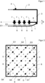
- FIG. 1 A first exemplary embodiment of a release element according to the invention is shown. Shown is a part of a sectional view with a cutting plane perpendicular to a flexible contact wall 1 of the release element.
- the flexible contact wall 1 is connected at the edge to a housing 2 of the detachment element, so that a vacuum chamber 3 is formed in the housing 2, which is delimited by the walls of the housing 2 and by the flexible contact wall 1.
- the detachment element has a suction opening 4, which in the present exemplary embodiment is formed on an upper wall of the housing 2. By sucking air out of the vacuum chamber 3 through the suction opening 4, a negative pressure can be created in the negative pressure chamber.
- the flexible contact wall 1 has a plurality of suction openings 5, as in Figure 2 visible:
- Figure 2 shows a top view from below of the flexible contact wall 1.
- the flexible contact wall 1 has a square shape with a plurality of suction openings 5, which are shown as open circles. For reasons of clarity, only three suction openings are marked with reference number 5 as an example.
- the surface of the flexible contact wall 1 covered by the suction openings 5 thus forms an air-permeable suction area for sucking in a semiconductor layer: When the flexible contact wall 1 is placed on a semiconductor layer, the semiconductor layer can be sucked onto the flexible contact wall 1 by means of the suction openings 5 by suction at the suction opening 4 and thus generating a negative pressure in the negative pressure chamber 3.
- the flexible contact wall 1 in the suction area is porous and therefore air-permeable.
- the porous design thus represents an alternative design of the air-permeable suction area to the design with suction openings. Suction openings can also be formed in a porous suction area.
- the semiconductor layer can be formed as a semiconductor layer known per se, in particular as a silicon layer, germanium layer or a multi-layer layer.
- the substrate is preferably a semiconductor substrate.
- the detachment unit according to the invention and the method according to the invention are suitable for detaching a silicon layer which has been produced on a silicon substrate.
- the use for other semiconductor layers, in particular a semiconductor layer which was produced on a germanium substrate is within the scope of the invention, for example epitaxially produced germanium layers or III/V compound semiconductor layers on a porosized germanium wafer as a substrate.
- the release element has a plurality of supports 6 spaced apart from one another.
- the supports 6 rest on the contact wall 1 with the ends facing the contact wall 1.
- the release element according to Figure 1 also has an actuator 7 for each of the supports 6.
- Each actuator is designed as an electrical linear actuator.
- the supports 6 can thus move linearly in a straight line with B in Figure 1 marked direction can be moved up and down.
- the supports are thus movable by means of the actuators and designed to interact with the contact wall, so that the flexible contact wall 1 can be selectively moved in partial areas by moving the supports.
- the actuators 7 are arranged on a perforated plate 8, which is connected to the housing 2 of the release element. As a result, the actuators 7 are rigidly relative arranged to the housing 2. However, fluid can pass through the holes in the perforated plate 8 up to the flexible contact wall 1, so that the vacuum chamber 3 extends up to the flexible contact wall 1.
- both the supports 6 and the actuators 7 are arranged in the vacuum chamber 3.
- the supports 6 can be moved into at least a first and a second position.
- the supports 6 are designed and arranged in such a way that the ends of the supports facing the contact wall lie in a first plane E1 in the first position and in a second plane E2 in the second position.
- These planes are perpendicular to the plane of the drawing and are identified by the reference symbols E1 and E2.
- the state is shown in which all actuators are extended, so that the ends of all supports 6 facing the flexible contact wall 1 are in the plane E1 and thus the flexible contact wall 1 is also in the area of the supports 6 in the plane E1.
- the plane E1 is parallel to the plane E2 and is spaced from it by 1000 ⁇ m.
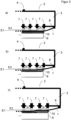
- Figure 3 are partial steps of an exemplary embodiment of a method according to the invention for removing a semiconductor layer from a substrate using the in Figure 1 shown detachment element shown.
- a substrate 9 is provided.
- the substrate 9 is designed as a semiconductor wafer, here designed as a silicon wafer, on the front side of which, which is always shown lying at the top in the figures, a porous separating layer was formed by etching.
- a semiconductor layer 10 was formed on the porous layer of the substrate 9 in a manner known per se.
- the semiconductor layer 10 was produced in in a manner known per se using silane, so that the semiconductor layer 10 is formed as a silicon layer.
- a method step B the semiconductor layer 10 is now detached from the substrate 9, as in partial figures a to c Figure 3 shown:
- All supports are moved to position E1.
- the release element with the flexible contact wall 1 is then arranged on the side of the semiconductor layer 10 facing away from the substrate 9.
- a negative pressure is generated in the vacuum chamber 3, so that the semiconductor layer 10 is sucked onto the flexible contact wall 1 and thus onto the detachment element due to the suction openings 5 formed in the flexible contact wall 1.
- Figure 3a shown This is in Figure 3a shown.
- Subregions of the flexible contact wall 1 are then successively removed from the substrate 9 in order to successively detach the semiconductor layer 10 from the substrate 9.
- the supports 6 are successively moved from right to left from position E1 to position E2.
- the adjacent support i.e. the second support from the right, is then moved to position E2, so that the semiconductor layer 10 also detaches from the substrate 9 in this area.
- each group of supports can be moved independently of the other groups, in the present exemplary embodiment, each support is assigned to its own actuator.
- the supports are mechanically coupled via rods, so that each group can be moved from position E1 to position E2 and vice versa by means of an actuator.
- the supports 6 are arranged along several straight, parallel lines and the actuators for these supports arranged along a line form a group.
- the supports 6 of all groups G1 to G7 are initially in the first position, so that their ends are in the plane E1.
- the actuators of group G1, then group G2 and then group G7 are successively moved to position E2, so that the in Figure 3 shown detachment process of the semiconductor layer 10 from the substrates 9 starting from the in Figure 2 top left corner up to the in Figure 2 bottom right corner.
- the flexible contact wall 1 thus carries out a wave movement, with the wave front parallel to the in Figure 2 straight lines shown in dashed lines, which mark the groups G1 to G7.
- Figure 4 shows a second embodiment of a release element, a modification to that in the Figures 1 to 3 shown first embodiment of a release element.
- the second exemplary embodiment is largely designed in the same way as the first exemplary embodiment. To avoid repetition, only the main differences will be discussed below: As in Figure 4 As can be seen, the flexible contact wall 1 is connected at the edge to the housing 2 in a position which corresponds to the extended supports 6 in the first position, that is to say the connection point between the flexible contact wall 1 and the housing 2 lies approximately in the plane E1.
- the detachment unit has a detachment element according to Figure 4a on, that is, according to the second exemplary embodiment.
- the detachment unit has a counter element 11. This counter element 11 is analogous to the second exemplary embodiment of a detachment element Figure 4a designed, but arranged mirror-inverted.
Landscapes
- Container, Conveyance, Adherence, Positioning, Of Wafer (AREA)
Description
- Die Erfindung betrifft ein Ablöseelement zum Ablösen einer Halbleiterschicht von einem Substrat gemäß Anspruch 1 sowie ein Verfahren zum Ablösen einer Halbleiterschicht von einem Substrat gemäß Anspruch 10.
- Bei der Herstellung von Halbleitersubstraten tritt üblicherweise ein hoher Materialverlust auf, wenn Halbleitersubstrate mittels Sägen aus einem Halbleiterblock erzeugt werden. Es sind daher Verfahren bekannt, bei welchen an einer Oberfläche eines wiederverwendbaren Trägersubstrats eine poröse Trennschicht erzeugt wird und auf der porösen Trennschicht mittels Epitaxie die Halbleiterschicht hergestellt wird. Anschließend wird die Halbleiterschicht mechanisch durch Krafteinwirkung im Bereich der porösen Trennschicht von dem Substrat abgetrennt.
- Es ist bekannt, manuell ein Saugelement an der Halbleiterschicht anzuordnen und mittels Krafteinwirkung durch einen Benutzer die Halbleiterschicht zu lösen. Ein solches Verfahren ist für eine industrielle Produktion von epitaktisch hergestellten Halbleiterschichten zu aufwendig und fehleranfällig.
- Aus
EP 1069602 A2 ist bekannt, eine Ablösewalze über die Halbleiterschicht zu rollen, wobei die Halbleiterschicht an der Ablösewalze anhaftet und hierdurch von dem Substrat gelöst wird. Nachteilig ist hierbei, dass für eine korrekte Führung der Ablöserolle ein aufwendiges Führungssystem notwendig ist, sodass insgesamt ein hoher Platzbedarf besteht. Insbesondere ist es zur Verringerung der Bruchgefahr der Halbleiterschicht beim Ablösen typischerweise notwendig, eine Ablöserolle mit einem großen Krümmungsradius, beispielsweise im Bereich 0,5 m bis 1 m vorzusehen, um eine zu starke Biegebelastung und hierdurch verursachte Bruchefahr zu vermeiden. - Weiterer Stand der Technik wird in den Dokumenten
US2011/0088845-A1 ,RU 2 683 808-C1 US2017/0239927-A1 gezeigt. - Der vorliegenden Erfindung liegt daher die Aufgabe zugrunde, ein Ablöseelement und ein Verfahren zum Ablösen einer Halbleiterschicht von einem Substrat zur Verfügung zu stellen, welches bei geringerem Platzbedarf industriell einsetzbar ist.
- Gelöst ist diese Aufgabe durch ein Ablöseelement zum Ablösen einer Halbleiterschicht von einem Substrat gemäß Anspruch 1 sowie ein Verfahren zum Ablösen einer Halbleiterschicht von einem Substrat gemäß Anspruch 10. Vorteilhafte Ausgestaltungen finden sich in den abhängigen Unteransprüchen. Die erfindungsgemäße Vorrichtung ist bevorzugt zur Durchführung mittels des erfindungsgemäßen Verfahrens, insbesondere einer bevorzugten Ausführungsform hiervon, ausgebildet. Das erfindungsgemäße Verfahren ist bevorzugt zur Durchführung mittels der erfindungsgemäßen Vorrichtung, insbesondere einer vorteilhaften Ausführungsform hiervon, ausgebildet.
- Das erfindungsgemäße Ablöseelement dient zum Ablösen einer Halbleiterschicht von einem Substrat. Es weist zumindest eine Unterdruckkammer mit zumindest einer Absaugöffnung und zumindest einem luftdurchlässigen Ansaugbereich zum Ansaugen der Halbleiterschicht auf.
- Wesentlich ist, dass die Unterdruckkammer eine flexible Kontaktwand zum Anlegen an die Halbleiterschicht aufweist und der Ansaugbereich in der Kontaktwand ausgebildet ist, dass das Ablöseelement eine Mehrzahl von zueinander beabstandeten Stützen und einen oder mehrere Aktoren aufweist, wobei die Stützen mit den der Kontaktwand zugewandten Enden an der Kontaktwand anliegen und mittels des Aktors oder Aktoren bewegbar sind und mit der Kontaktwand zusammenwirkend ausgebildet sind, um die flexible Kontaktwand zumindest in Teilbereichen zu bewegen.
- Das erfindungsgemäße Ablöseelement ist somit geeignet, die Halbleiterschicht an der flexiblen Kontaktwand anzusaugen, da die flexible Kontaktwand Teil der Unterdruckkammer ist und den Ansaugbereich aufweist. Darüber hinaus kann die Kontaktwand zumindest in Teilbereichen mittels des oder der Aktoren bewegt werden.
- Mittels des Ablöseelements ist es somit möglich, eine Ablösekraft auf die Halbleiterschicht einzuwirken, ohne dass eine Relativbewegung des Ablöseelements zu dem Substrat erfolgt. Es kann lediglich die flexible Kontaktwand zumindest in Teilbereichen mittels des oder der Aktoren relativ zu dem Substrat bewegt werden, um die Ablösekraft zu bewirken.
- Hierdurch ist nicht nur ein platzsparender und robuster Aufbau möglich. Darüber hinaus kann durch den oder die Aktoren ein für den Ablösegang vorteilhaftes Ablösemuster der Ablösekraft erzielt werden.
- Die eingangs gestellte Aufgabe ist weiterhin durch ein Verfahren zum Ablösen einer Halbleiterschicht von einem Substrat gelöst. Das Verfahren weist folgende Verfahrensschritte auf:
In einem Verfahrensschritt A erfolgt ein Bereitstellen eines Substrats mit einer an dem Substrat angeordneten Halbleiterschicht. In einem Verfahrensschritt B erfolgt ein Ablösen der Halbleiterschicht von dem Substrat. - Wesentlich ist, dass im Verfahrensschritt B eine flexible Kontaktwand an die Halbleiterschicht angelegt wird, die Halbleiterschicht an die Kontaktwand angesaugt wird und die Kontaktwand in mehrere Teilbereiche unterteilt ist, welche sukzessiv von dem Substrat entfernt werden, um die Halbleiterschicht sukzessiv von dem Substrat zu lösen.
- Hierdurch wird die vorgenannte raumsparende Ausgestaltung einer entsprechenden Vorrichtung zur Durchführung dieses Verfahrens erzielt. Darüber hinaus ermöglicht das sukzessive Entfernen mehrerer Teilbereiche der Kontaktwand von dem Substrat eine vorteilhafte Wahl der Ablösebewegung und der damit auf die Halbleiterschicht einwirkenden Ablösekräfte.
- Es liegt im Rahmen der Erfindung, dass die flexible Kontaktwand in zumindest einem Bereich, bevorzugt in mehreren Bereichen, außerhalb der Unterdrucckammer fortgeführt wird und insbesondere, dass eine oder mehrere Stützen in diesen Bereichen an der Kontaktwand anliegen. Dies ermöglicht einen einfacheren Austausch der Stützen und insbesondere treten etwaige Fremdkörper wie beispielsweise Schmiermittel der Stützen nicht in die Unterdruckkammer ein.
- In einer weiteren vorteilhaften Ausgestaltung ist eine oder mehrere Stützen in der Unterdruckkammer angeordnet. Hierdurch ergibt sich ein konstruktiv einfacher Aufbau. Insbesondere ist es vorteilhaft, dass alle Stützen in der Unterdruckkammer angeordnet sind.
- In einer vorteilhaften Weiterbildung ist zusätzlich der Aktor oder die Aktoren zum Bewegen der Stützen in der Unterdruckkammer angeordnet, sodass sich eine weitere konstruktive Vereinfachung des Aufbaus ergibt.
- Die Stützen sind bevorzugt mittels des oder der Aktoren in zumindest eine erste und eine zweite Position bewegbar, wobei die Stützen derart ausgebildet und angeordnet sind, dass die der Kontaktwand zugewandten Enden der Stützwand in der ersten Position in einer ersten Ebene und in der zweiten Position in einer zweiten, zu der ersten Ebene parallelen Ebene liegen.
- Hierdurch ergibt sich eine konstruktiv einfach realisierbare Ablösebewegung. Darüber hinaus weisen Stützen, die gemeinsam in der ersten Position oder gemeinsam in der zweiten Position angeordnet sind, keinen Höhenunterschied relativ zueinander auf, sodass keine oder allenfalls eine geringe Krafteinwirkung auf die Halbleiterschicht zwischen diesen Stützen erfolgt und somit die Bruchgefahr verringert wird.
- Vorteilhafterweise sind die Stützen in eine Mehrzahl von Gruppen unterteilt, wobei jede Gruppe von Stützen unabhängig von der anderen Gruppe bewegbar ist. Hierdurch ist in konstruktiv einfacher Weise eine Ablösebewegung der flexiblen Kontaktwand vorgebbar, indem sukzessiv für die einzelnen Gruppen nacheinander eine Bewegung mittels dies oder Aktoren durchgeführt wird.
- Hierbei ist es insbesondere vorteilhaft, dass das Ablöseelement für jede Gruppe zumindest einen, bevorzugt genau einen Aktor aufweist, um die Stützen dieser Gruppe zu bewegen.
- Insbesondere ist es vorteilhaft, dass die Stützen entlang mehrerer geradliniger, paralleler Linien angeordnet sind und die entlang einer Linie angeordneten Stützen eine Gruppe bilden. Hierdurch lässt sich in einfacher Weise eine Wellenbewegung der flexiblen Kontaktwand mit einer geradlinigen Wellenfront durchführen. Eine solche Wellenbewegung ist zum bruchfreien Ablösen der Kontaktschicht von dem Trägersubstrat geeignet.
- In einer vorteilhaften Weiterbildung ist jede Stütze unabhängig von den anderen Stützen bewegbar. Hierdurch lassen sich auch komplexe Ablösebewegungen der flexiblen Kontaktwand durchführen. Insbesondere ist es zum Erzielen eines konstruktiv einfachen Aufbaus vorteilhaft, dass das Ablöseelement für jede Stütze einen separaten Aktor aufweist, um die Durchführung komplexer Ablösebewegungen der flexiblen Kontaktwand insbesondere mit nicht geradlinigen Wellenfronten zu ermöglichen.
- Vorteilhafterweise sind der Aktor oder die Aktoren als Stellantriebe, insbesondere als elektromagnetische oder piezoelektrische Stellantriebe, ausgebildet. Solche Stellantriebe sind an sich bekannt und können handelsüblich in kompakter Bauform erworben werden, sodass ein kostengünstiger Aufbau ohne Entwicklungsaufwand hinsichtlich der Aktoren ermöglicht wird.
- Untersuchungen der Anmelderin zeigen, dass für typische Ablösevorgänge von epitaktisch aufgewachsenen Halbleiterschichten vorteilhafterweise die Stützen mittels des oder der Aktoren um einen Verfahrweg im Bereich 50 µm bis 3000 µm, insbesondere 500 µm bis 1500 µm verschiebbar sind.
- Die eingangs gestellte Aufgabe ist weiterhin durch eine Ablöseeinheit zum Ablösen einer Halbleiterschicht von einem Substrat gelöst. Die Ablöseeinheit weist ein erfindungsgemäßes Ablöseelement, insbesondere eine bevorzugte Ausführungsform hiervon, auf und ein Gegenelement, welches zumindest einen luftdurchlässigen Ansaugbereich zum Ansaugen des Substrats aufweist. Hierdurch wird somit ein Ansaugen des Substrats einerseits mittels des Gegenelementes und ein Ansaugen der Halbleiterschicht andererseits mittels der flexiblen Kontaktwand des Ablöseelements ermöglicht, sodass eine Ablösekraft erzielbar ist, welche bevorzugt senkrecht zur Trennschicht zwischen Halbleiterschicht und Substrat und ausgehend von dem Substrat in Richtung der Halbleiterschicht gerichtet ist.
- Vorteilhafterweise ist das Gegenelement analog zu dem Ablöseelement, insbesondere einer bevorzugten Ausführungsform hiervon, ausgebildet, wobei die flexible Kontaktwand des Gegenelementes zum Anliegen an das Substrat ausgebildet ist. Hierdurch wird ein sicheres Ansaugen auch bei unebener Substratrückseite, an welcher das Gegenelement anliegt, ermöglicht.
- Bei dem erfindungsgemäßen Verfahren weisen vorteilhafterweise die Teilbereiche eine geradlinige Längserstreckung auf und die Längserstreckungen der Teilbereiche sind zueinander parallel. Hierdurch lässt sich die zuvor beschriebene, vorteilhafte Wellenbewegung mit geradliniger Wellenfront erzielen.
- Typische Halbleiterschichten weisen eine im Wesentlichen rechteckige, insbesondere quadratische Form auf. Vorteilhafterweise beginnt in Verfahrensschritt E das Ablösen im Bereich einer Ecke der Halbleiterschicht. Hierdurch wird eine vorteilhafte Ablösebewegung erzielt, welche die Bruchgefahr verringert. Ebenso kann das erfindungsgemäße Ablöseelement und das erfindungsgemäße Verfahren zur Anwendung bei anderen Formen von Halbleiterschichten, insbesondere runde Formen ausgebildet sein. Hierbei ist bevorzugt der Ansaugbereich auf die Form der abzulösenden Halbleiterschicht angepasst, d.h. bevorzugt kleiner oder gleich groß wie die abzulösende Halbleiterschicht, so dass keine Luft in einem nicht von der Halbleiterschicht bedeckten Bereich des Ansaugbereiches in die Unterdruckkammer eintritt.
- Im Falle von runden Formen der Halbleiterschicht beginnt im Verfahrensschritt E bevorzugt das Ablösen bevorzugt an einer Ecke der sog. Flat (abgeflachte Seite des zugehörigen Substrats zur Identifikation der kristallographischen Orientierung) oder Notch (in das zugehörige Substrat eingefräste Kerbe zur Identifikation der kristallographischen Orientierung), falls solche Markierungen vorhanden sind. Vorteilhafterweise werden zum Ablösen die Teilbereiche der Kontaktwand um eine Strecke im Bereich 50 µm bis 3000 µm, insbesondere 500 µm bis 1500 µm bewegt.
- Das Ablösen mittels des erfindungsgemäßen Verfahrens, insbesondere einer bevorzugten Ausführungsform hiervon, erfolgt bevorzugt mittels eines erfindungsgemäßen Ablöseelementes, insbesondere mittels der zuvor beschriebenen Ablöseeinheit.
- Die Halbleiterschicht wird bevorzugt epitaktisch auf das Substrat aufgebracht. Vorteilhafterweise wird zunächst auf einer Oberfläche des Substrats eine poröse Trennschicht erzeugt, insbesondere bevorzugt in an sich bekannter Weise mittels Ätzen und anschließend epitaktisch die Halbleiterschicht auf der Trennschicht ausgebildet.
- Der luftdurchlässige Ansaugbereich von Ablöseelement und/oder Gegenelement weist bevorzugt eine Mehrzahl von Ansaugöffnungen auf. Durch die Ansaugöffnungen kann Luft in die Unterdruckkammer gesaugt und somit die Halbleiterschicht an die flexible Kontaktwand von Ablöseelement und/oder Gegenelement angesaugt werden. In einer alternativen vorteilhaften Ausführungsform ist der luftdurchlässige Ansaugbereich von Ablöseelement und/oder Gegenelement als poröser Bereich ausgebildet, so dass Luft durch den porösen Bereich hindurchtreten kann und hierdurch ein Ansaugen ermöglicht wird. Ebenso liegt die Kombination durch Ausbilden eines porösen Ansaugbereiches, welcher zusätzlich Ansaugöffnungen aufweist, im Rahmen der Erfindung.
- Weitere vorteilhafte Merkmale und Ausführungsformen werden im Folgenden anhand von Ausführungsbeispielen und den Figuren erläutert. Dabei zeigt:
- Figur 1
- eine Teilschnittdarstellung eines ersten Ausführungsbeispiels des erfindungsgemäßen Ablöseelements;
- Figur 2
- eine Schnittdarstellung senkrecht zur Figurenebene in
Figur 1 ; - Figur 3
- Teilschritte eines Ausführungsbeispiels des erfindungsgemäßen Verfahrens zum Ablösen einer Halbleiterschicht von einem Substrat mittels des in
Figur 1 dargestellten ersten Ausführungsbeispiels eines Ablöseelements; - Figur 4
- ein zweites Ausführungsbeispiel eines erfindungsgemäßen Ablöseelementes und ein Ausführungsbeispiel einer erfindungsgemäßen Ablöseeinheit.
- Sämtliche Figuren zeigen schematische, nicht maßstabsgetreue Darstellungen. Gleiche Bezugszeichen in den Figuren bezeichnen gleiche oder gleichwirkende Elemente.
- In
Figur 1 ist ein erstes Ausführungsbeispiel eines erfindungsgemäßen Ablöseelementes gezeigt. Dargestellt ist ein Teil einer Schnittdarstellung mit einer Schnittebene senkrecht zu einer flexiblen Kontaktwand 1 des Ablöseelements. Die flexible Kontaktwand 1 ist randseitig mit einem Gehäuse 2 des Ablöseelementes verbunden, sodass in dem Gehäuse 2 eine Unterdruckkammer 3 ausgebildet ist, welche durch die Wände des Gehäuses 2 sowie durch die flexible Kontaktwand 1 begrenzt ist. - Zur besseren Darstellbarkeit ist in den
Figuren 1 ,3 und4 jeweils nur ein rechter Teilbereich der Schnittdarstellung gezeigt. Das Ablöseelement setzt sich jeweils nach links fort, wie durch die Punktlinien angedeutet. - Das Ablöseelement weist eine Absaugöffnung 4 auf, welche bei dem vorliegenden Ausführungsbeispiel an einer oberen Wand des Gehäuses 2 ausgebildet ist. Durch Absaugen von Luft durch die Absaugöffnung 4 aus der Unterdruckkammer 3 kann ein Unterdruck in der Unterdruckkammer hergestellt werden.
- Die flexible Kontaktwand 1 weist eine Mehrzahl von Ansaugöffnungen 5 auf, wie in
Figur 2 ersichtlich:
Figur 2 zeigt eine Draufsicht von unten auf die flexible Kontaktwand 1. Die flexible Kontaktwand 1 weist eine quadratische Form auf mit einer Vielzahl von Ansaugöffnungen 5, welche als offene Kreise dargestellt sind. Aus Gründen der Übersichtlichkeit sind exemplarisch lediglich drei Ansaugöffnungen mit Bezugszeichen 5 gekennzeichnet. Die von den Ansaugöffnungen 5 abgedeckte Fläche der flexiblen Kontaktwand 1 bildet somit einen luftdurchlässigen Ansaugbereich aus, zum Ansaugen einer Halbleiterschicht:
Bei Auflegen der flexiblen Kontaktwand 1 auf eine Halbleiterschicht kann somit durch Absaugen an der Absaugöffnung 4 und somit Erzeugen eines Unterdrucks in der Unterdruckkammer 3 die Halbleiterschicht an die flexible Kontaktwand 1 mittels der Ansaugöffnungen 5 angesaugt werden. - In einer alternativen Ausführungsform dieses Ausführungsbeispiels ist die flexible Kontaktwand 1 in dem Ansaugbereich porös und somit luftdurchlässig ausgebildet. Die poröse Ausbildung stellt somit eine alternative Ausbildung des luftdurchlässigen Ansaugbereiches zu der Ausbildung mit Ansaugöffnungen dar. Ebenso können Ansaugöffnungen in einem porösen Ansaugbereich ausgebildet werden.
- Die Halbleiterschicht kann als an sich bekannte Halbleiterschicht ausgebildet sein, insbesondere als Siliziumschicht, Germaniumschicht oder eine mehrlagige Schicht. Das Substrat ist bevorzugt ein Halbleitersubstrat.
- Insbesondere sind die erfindungsgemäße Ablöseeinheit und das erfindungsgemäße Verfahren zum Ablösen einer Siliziumschicht geeignet, welche auf einem Siliziumsubstrat erzeugt wurde. Ebenso liegt die Verwendung für andere Halbleiterschichten, insbesondere eine Halbleiterschicht, welche auf einem Germaniumsubstrat erzeugt wurde, im Rahmen der Erfindung, beispielsweise epitaktisch erzeugte Germaniumschichten oder III/V Verbindungshalbleiterschichten auf einem porosiziertem Germanium-Wafer als Substrat.
- Wie in
Figur 1 ersichtlich, weist das Ablöseelement eine Mehrzahl von zueinander beabstandeter Stützen 6 auf. Die Stützen 6 liegen mit den der Kontaktwand 1 zugewandten Enden an der Kontaktwand 1 an. - Das Ablöseelement gemäß
Figur 1 weist weiterhin für jede der Stützen 6 jeweils einen Aktor 7 auf. Jeder Aktor ist als elektrischer Linearaktor ausgebildet. - Mittels der Aktoren 7 können die Stützen 6 somit linear geradlinig in der mit B in
Figur 1 gekennzeichneten Richtung auf und ab bewegt werden. - Die Stützen sind somit mittels der Aktoren bewegbar und mit der Kontaktwand zusammenwirkend ausgebildet, sodass die flexible Kontaktwand 1 selektiv in Teilbereichen durch Verfahren der Stützen bewegt werden kann.
- Die Aktoren 7 sind an einer Lochplatte 8 angeordnet, welche mit dem Gehäuse 2 des Ablöseelementes verbunden ist. Hierdurch sind die Aktoren 7 starr relativ zu dem Gehäuse 2 angeordnet. Durch die Löcher der Lochplatte 8 kann jedoch Fluid bis zu der flexiblen Kontaktwand 1 hindurchtreten, sodass sich die Unterdruckkammer 3 bis zu der flexiblen Kontaktwand 1 erstreckt.
- In
Figur 2 sind zur besseren Verständlichkeit die Auflagepunkte der Stützen 6 an der flexiblen Kontaktwand 1 durch geschlossene Kreise gekennzeichnet. Auch hier sind zur besseren Übersichtlichkeit lediglich drei geschlossene Kreise durch Bezugszeichen 6 gekennzeichnet. - In
Figur 1 ersichtlich, sind bei dem gezeigten ersten Ausführungsbeispiel sowohl die Stützen 6 als auch die Aktoren 7 in der Unterdruckkammer 3 angeordnet. - Mittels der Aktoren 7 sind die Stützen 6 in zumindest eine erste und eine zweite Position bewegbar. Die Stützen 6 sind dabei derart ausgebildet und angeordnet, dass die der Kontaktwand zugewandten Enden der Stützen in der ersten Position in einer ersten Ebene E1 und in der zweiten Position in einer zweiten Ebene E2 liegen. In
Figur 1 stehen diese Ebenen senkrecht zur Zeichenebene und sind durch die Bezugszeichen E1 und E2 gekennzeichnet. Wie inFigur 1 ersichtlich, ist der Zustand dargestellt, bei welchem alle Aktoren ausgefahren sind, sodass die der flexiblen Kontaktwand 1 zugewandten Enden aller Stützen 6 sich in der Ebene E1 befinden und sich somit auch die flexible Kontaktwand 1 im Bereich der Stützen 6 in der Ebene E1 befindet. - Die Ebene E1 ist parallel zu der Ebene E2 und zu dieser um 1000 µm beabstandet.
- In
Figur 3 sind Teilschritte eines Ausführungsbeispiels eines erfindungsgemäßen Verfahrens zum Ablösen einer Halbleiterschicht von einem Substrat mittels des inFigur 1 gezeigten Ablöseelementes dargestellt. - In einem Verfahrensschritt A wird ein Substrat 9 bereitgestellt. Das Substrat 9 ist als Halbleiterwafer ausgebildet, vorliegend als Siliziumwafer ausgebildet, an dessen Vorderseite, welche in den Figuren stets oben liegend dargestellt ist, mittels Ätzen eine poröse Trennschicht ausgebildet wurde. Mittels Epitaxie wurde in an sich bekannter Weise eine Halbleiterschicht 10 auf der porösen Schicht des Substrats 9 ausgebildet. Die Herstellung der Halbleiterschicht 10 erfolgte in an sich bekannter Weise unter der Verwendung von Silan, sodass die Halbleiterschicht 10 als Siliziumschicht ausgebildet ist.
- In einem Verfahrensschritt B erfolgt nun ein Ablösen der Halbleiterschicht 10 von dem Substrat 9, wie in den Teilfiguren a bis c der
Figur 3 gezeigt:
Zunächst werden alle Stützen in die Position E1 gefahren. Anschließend wird das Ablöseelement mit der flexiblen Kontaktwand 1 an der dem Substrat 9 abgewandten Seite der Halbleiterschicht 10 angeordnet. Mittels Absaugen durch die Absaugöffnung 4 wird in der Unterdruckkammer 3 ein Unterdruck erzeugt, sodass aufgrund der in der flexiblen Kontaktwand 1 ausgebildeten Ansaugöffnungen 5 die Halbleiterschicht 10 an die flexible Kontaktwand 1 und somit an das Ablöseelement angesaugt wird. Dies ist inFigur 3a dargestellt. - Anschließend werden Teilbereiche der flexiblen Kontaktwand 1 sukzessive von dem Substrat 9 entfernt, um die Halbleiterschicht 10 sukzessiv von dem Substrat 9 zu lösen. In der Darstellung gemäß
Figur 3 werden sukzessiv die Stützen 6 von rechts nach links abfolgend jeweils von der Position E1 in die Position E2 verfahren. - In
Figur 3b ist ein Zwischenzustand dargestellt, bei welchem lediglich die rechte Stütze 6 mittels des zugeordneten Aktors 7 in die Position E2 verfahren wurde. Aufgrund des Unterdrucks in der Unterdruckkammer 3 bewegt sich auch die flexible Kontaktwand 1 in demjenigen Teilbereich, welcher an der rechten Stütze 6 anliegt, nach oben in die Position E2. Hierdurch löst sich die Halbleiterschicht 10 im rechten Randbereich von dem Substrat 9. - Anschließend wird die benachbarte Stütze, das heißt die zweite Stütze von rechts, in die Position E2 verfahren, sodass sich auch in diesem Bereich die Halbleiterschicht 10 von dem Substrat 9 löst. Dies ist in
Figur 3c dargestellt. Sukzessive werden nun nacheinander alle Stützen 6 in die Position E2 verfahren, sodass schließlich die Halbleiterschicht 10 vollständig von dem Substrat 9 gelöst ist. - Die Stützen sind hierbei in mehrere Gruppen unterteilt, wie in
Figur 2 ersichtlich. Jede Gruppe von Stützen ist unabhängig von den anderen Gruppen bewegbar, bei dem vorliegenden Ausführungsbeispiel dadurch, dass jede Stütze einem eigenen Aktor zugeordnet ist. In einer Abwandlung des Ausführungsbeispiels sind die Stützen über Stangen mechanisch gekoppelt, sodass jede Gruppe mittels eines Aktors aus der Position E1 in die Position E2 und umgekehrt bewegt werden kann. - Die Stützen 6 sind entlang mehrerer geradliniger, paralleler Linien angeordnet und die entlang einer Linie angeordneten Aktoren zu diesen Stützen bilden eine Gruppe.
- Wie in
Figur 2 ersichtlich, verlaufen die gestrichelt dargestellten parallelen Linien, welche die Gruppen definieren, diagonal zu der quadratischen Ausgestaltung der flexiblen Kontaktwand 1. Bei dem inFigur 2 dargestellten Ausführungsbeispiel liegen somit sieben Gruppen G1 bis G7 vor, wobei die Gruppen G1 und G7 jeweils lediglich eine Stütze 6 mit zugeordnetem Aktor 7 umfassen. - Bei dem Ablösevorgang befinden sich zunächst die Stützen 6 aller Gruppen G1 bis G7 in der ersten Position, sodass deren Enden sich in der Ebene E1 befinden.
- Nun werden in aufsteigender Folge zunächst die Aktoren der Gruppe G1, anschließend der Gruppe G2 und weiterfolgend bis zur Gruppe G7 sukzessive in die Position E2 verfahren, sodass der in
Figur 3 gezeigte Ablösevorgang der Halbleiterschicht 10 von den Substraten 9 ausgehend von der inFigur 2 links oben liegenden Ecke bis zu der inFigur 2 rechts unten liegenden Ecke erfolgt. Die flexible Kontaktwand 1 führt somit eine Wellenbewegung durch, wobei die Wellenfront parallel zu den inFigur 2 gestrichelt dargestellten geraden Linien verläuft, welche die Gruppen G1 bis G7 markieren. - In
Figur 1 ist ersichtlich, dass die flexible Kontaktwand 1 am Rand mit dem Gehäuse 2 in einer Position verbunden ist, welche in etwa in der Ebene E2 liegt. - Hierdurch ergibt sich eine kostengünstige Ausgestaltung, allerdings besteht in dem Zustand, in welchem alle Stützen in die Position 1 gefahren sind und deren Enden sich somit in der Ebene E1 befinden, aufgrund Spannungseinwirkung der flexiblen Kontaktwand 1 eine deutliche Krafteinwirkung auf die rechte Stütze 6 in
Figur 1 . Durch Wahl eines entsprechend robusten Aktors kann auch in dieser Konfiguration ein dauerhafter Betrieb gewährleistet werden. -
Figur 4 zeigt als zweites Ausführungsbeispiel eines Ablöseelementes eine Abwandlung zu dem in denFiguren 1 bis 3 gezeigten ersten Ausführungsbeispiel eines Ablöseelementes. - Das zweite Ausführungsbeispiel ist weitgehend gleich zu dem ersten Ausführungsbeispiel ausgebildet. Zur Vermeidung von Wiederholungen wird daher im Folgenden lediglich auf die wesentlichen Unterschiede eingegangen:
Wie inFigur 4 ersichtlich, ist die flexible Kontaktwand 1 am Rand mit dem Gehäuse 2 in einer Position verbunden, welche den ausgefahrenen Stützen 6 in der ersten Position entspricht, das heißt der Verbindungsort zwischen flexibler Kontaktwand 1 und Gehäuse 2 liegt in etwa in der Ebene E1. - Werden nun die Stützen 6 eingefahren, sodass sich deren Enden in der Position E2 befinden, so wirkt auf die randständigen Stützen und zugeordneten Aktoren eine geringere Kraft verglichen mit dem ersten Ausführungsbeispiel.
- In
Figur 4b ist schließlich ein Ausführungsbeispiel einer erfindungsgemäßen Ablöseeinheit dargestellt. Die Ablöseeinheit weist vorliegend ein Ablöseelement gemäßFigur 4a auf, das heißt gemäß des zweiten Ausführungsbeispiels. Zusätzlich weist die Ablöseeinheit ein Gegenelement 11 auf. Dieses Gegenelement 11 ist analog zu dem zweiten Ausführungsbeispiel eines Ablöseelementes gemäßFigur 4a ausgebildet, jedoch spiegelverkehrt angeordnet. - Wie in
Figur 4b ersichtlich, kann während des Ablösevorgangs somit mittels des oberen Ablöseelementes analog zu der Darstellung inFigur 3 sukzessive vom rechten Rand ausgehend die Halbleiterschicht 10 von dem Substrat 9 gelöst werden. Gleichzeitig wird das Substrat 9 mittels des Gegenelementes 11 fixiert. - Der Schutzbereich des europäischen Patents wird durch die Patentansprüche bestimmt.
-
- 1
- flexible Kontaktwand
- 2
- Gehäuse
- 3
- Unterdruckkammer
- 4
- Absaugöffnung
- 5
- Ansaugöffnungen
- 6
- Stützen
- 7
- Aktor
- 8
- Lochplatte
- 9
- Substrat
- 10
- Halbleiterschicht
- 11
- Gegenelement
Claims (15)
- Ablöseelement zum Ablösen einer Halbleiterschicht (10) von einem Substrat (9),mit zumindest einer Unterdruckkammer (3) mit zumindest einer Absaugöffnung (4) und zumindest einem luftdurchlässigen Ansaugbereich zum Ansaugen der Halbleiterschicht (10), wobeidie Unterdruckkammer eine flexible Kontaktwand (1) zum Anlegen an die Halbleiterschicht (10) aufweist und der Ansaugbereich in der Kontaktwand ausgebildet ist,wobei das Ablöseelement eine Mehrzahl von zueinander beabstandeten Stützen (6) und einen oder mehrere Aktoren (7) aufweist, wobei die Stützen (6) mit den der Kontaktwand zugewandten Enden an der Kontaktwand anliegen und mittels des Aktors (7) oder der Aktoren (7) bewegbar und mit der Kontaktwand zusammenwirkend ausgebildet sind, um die flexible Kontaktwand (1) zumindest in Teilbereichen zu bewegen.
- Ablöseelement nach Anspruch 1,
dadurch gekennzeichnet,
dass die Stützen (6) in der Unterdruckkammer (3) angeordnet sind, insbesondere, dass die Stützen (6) und der Aktor (7) oder die Aktoren (7) zum Bewegen der Stützen (6) in der Unterdruckkammer (3) angeordnet sind. - Ablöseelement nach Anspruch 1,
dadurch gekennzeichnet,
die Stützen (6) mittels des oder der Aktoren (7) in zumindest eine erste und eine zweite Position bewegbar sind, wobei die Stützen (6) derart ausgebildet und angeordnet sind, dass die der Kontaktwand zugewandten Enden der Stützwand in der ersten Position in einer ersten Ebene und in der zweiten Position in einer zweiten, zu der ersten Ebene parallele Ebene liegen. - Ablöseelement nach einem der vorangegangen Ansprüche,
dadurch gekennzeichnet,dass die Stützen (6) in eine Mehrzahl von Gruppen untereilt sind, wobei jede Gruppe von Stützen (6) unabhängig von den anderen Gruppen bewegbar ist, insbesondere, dass das Ablöseelement für jede Gruppe zumindest einen, bevorzugt genau einen Aktor (7) aufweist, um die Stützen (6) dieser Gruppe zu bewegen,bevorzugt, dass jede Stütze (6) unabhängig von den anderen Stützen (6) bewegbar ist, insbesondere, dass das Ablöseelement für jede Stütze einen separaten Aktor (7) aufweist. - Ablöseelement nach Anspruch 4,
dadurch gekennzeichnet,
dass die Stützen (6) entlang mehrerer geradliniger, paralleler Linien angeordnet sind und die entlang einer Linie angeordneten Aktoren (7) eine Gruppe bilden. - Ablöseelement nach einem der vorangegangenen Ansprüche,
dadurch gekennzeichnet,
dass der oder die Aktoren (7) als Stellantriebe, insbesondere als elektromagnetische Stellantriebe ausgebildet sind. - Ablöseelement nach einem der vorangegangenen Ansprüche,
dadurch gekennzeichnet,
die Stützen (6) mittels des oder der Aktoren (7) um einen Verfahrweg im Bereich 50 µm bis 3000 µm, insbesondere 500 µm bis 1500 µm verschiebbar sind. - Ablöseeinheit zum Ablösen zum Ablösen einer Halbleiterschicht (10) von einem Substrat (9),
mit einem Ablöseelement nach einem der vorangegangenen Ansprüche und mit einem Gegenelement, welches zumindest einen luftdurchlässigen Ansaugbereich zum Ansaugen des Substrats aufweist. - Ablöseeinheit nach Anspruch 8,
dadurch gekennzeichnet,
dass das Gegenelement (11) wie ein Ablöseelement gemäß einem der Ansprüche 1 bis 7 ausgebildet ist, wobei die flexible Kontaktwand (1) des Gegenelements zum Anlegen an das Substrat (9) ausgebildet ist. - Verfahren zum Ablösen einer Halbleiterschicht (10) von einem Substrat, mit den VerfahrensschrittenA. Bereitstellen eines Substrats (9), mit einer an dem Substrat (9) angeordneten Halbleiterschicht (10),B. Ablösen der Halbleiterschicht (10) von dem Substrat (9),wobei in Verfahrensschritt B eine flexible Kontaktwand (1) an die Halbleiterschicht (10) angelegt wird, die Halbleiterschicht (10) an die Kontaktwand angesaugt wird und die Kontaktwand in mehrere Teilbereiche unterteilt ist, welche sukzessiv von dem Substrat (9) entfernt werden, um die Halbleiterschicht (10) sukzessiv von dem Substrat (9) zu lösen.
- Verfahren nach Anspruch 10,
dadurch gekennzeichnet,
dass die Teilbereiche eine geradlinige Längserstreckung aufweisen und die Längserstreckungen der Teilbereiche parallel zueinander sind. - Verfahren nach einem der Ansprüche 10 bis 11,
dadurch gekennzeichnet,
dass die Halbleiterschicht (10) eine im Wesentlichen rechteckige, insbesondere quadratische Form aufweist und im Bereich einer Ecke der Halbleiterschicht (10) das Ablösen in Verfahrensschritt B beginnt. - Verfahren nach einem der Ansprüche 10 bis 12,
dadurch gekennzeichnet,
dass zum Ablösen die Teilbereiche der Kontaktwand um eine Strecke im Bereich 50 µm bis 3000 µm, insbesondere 500 µm bis 1500 µm entfernt werden. - Verfahren nach einem der Ansprüche 10 bis 13,
dadurch gekennzeichnet,
dass das Ablösen mittels eines Ablöseelements gemäß einem der Ansprüche 1 bis 7, insbesondere mittels einer Ablöseeinheit gemäß einem der Ansprüche 8 bis 9 erfolgt. - Verfahren nach einem der Ansprüche 10 bis 14,
dadurch gekennzeichnet,
dass die Halbleiterschicht (10) epitaktisch auf das Substrat (9) aufgebracht wird, insbesondere, dass an dem Substrat (9) eine Trennschicht ausgebildet wird und die Halbleiterschicht (10) auf die Trennschicht aufgebracht wird.
Applications Claiming Priority (2)
| Application Number | Priority Date | Filing Date | Title |
|---|---|---|---|
| DE102019135499.4A DE102019135499B3 (de) | 2019-12-20 | 2019-12-20 | Ablöseelement, Ablöseeinheit und Verfahren zum Ablösen einer Halbleiterschicht von einem Substrat |
| PCT/EP2020/081413 WO2021121769A1 (de) | 2019-12-20 | 2020-11-09 | Ablöseelement und verfahren zum ablösen einer halbleiterschicht von einem substrat |
Publications (2)
| Publication Number | Publication Date |
|---|---|
| EP4078667A1 EP4078667A1 (de) | 2022-10-26 |
| EP4078667B1 true EP4078667B1 (de) | 2023-12-27 |
Family
ID=73288576
Family Applications (1)
| Application Number | Title | Priority Date | Filing Date |
|---|---|---|---|
| EP20804202.8A Active EP4078667B1 (de) | 2019-12-20 | 2020-11-09 | Ablöseelement und verfahren zum ablösen einer halbleiterschicht von einem substrat |
Country Status (4)
| Country | Link |
|---|---|
| EP (1) | EP4078667B1 (de) |
| DE (1) | DE102019135499B3 (de) |
| ES (1) | ES2970182T3 (de) |
| WO (1) | WO2021121769A1 (de) |
Cited By (1)
| Publication number | Priority date | Publication date | Assignee | Title |
|---|---|---|---|---|
| TWI922377B (zh) | 2024-09-25 | 2026-04-11 | 日商龍雲股份有限公司 | 腔室裝置及位置調整機構 |
Family Cites Families (10)
| Publication number | Priority date | Publication date | Assignee | Title |
|---|---|---|---|---|
| JPH10233430A (ja) * | 1997-02-19 | 1998-09-02 | Nitto Denko Corp | 粘着テープ貼付け装置 |
| US6452091B1 (en) * | 1999-07-14 | 2002-09-17 | Canon Kabushiki Kaisha | Method of producing thin-film single-crystal device, solar cell module and method of producing the same |
| DE10128923A1 (de) * | 2001-06-15 | 2003-01-23 | Philips Corp Intellectual Pty | Verfahren zum Umsetzen eines im wesentlichen scheibenförmigen Werkstücks und Vorrichtung zur Durchführung dieses Verfahrens |
| US7665204B2 (en) * | 2006-10-16 | 2010-02-23 | Asm Assembly Automation Ltd. | Die detachment apparatus comprising pre-peeling structure |
| DE102008018536B4 (de) * | 2008-04-12 | 2020-08-13 | Erich Thallner | Vorrichtung und Verfahren zum Aufbringen und/oder Ablösen eines Wafers auf einen/von einem Träger |
| US8470130B2 (en) * | 2009-10-20 | 2013-06-25 | Asm Assembly Automation Ltd | Universal die detachment apparatus |
| JP5563423B2 (ja) * | 2010-10-19 | 2014-07-30 | リンテック株式会社 | シート貼付装置および貼付方法 |
| CN104247068B (zh) * | 2012-04-23 | 2017-12-05 | 南洋理工大学 | 用于分离多层结构的装置和方法 |
| EP3211662A1 (de) * | 2016-02-23 | 2017-08-30 | Nokia Technologies Oy | Vorrichtung und entsprechende verfahren |
| RU2683808C1 (ru) * | 2018-04-19 | 2019-04-02 | Федеральное государственное бюджетное учреждение науки Институт физики полупроводников им. А.В. Ржанова Сибирского отделения Российской академии наук (ИФП СО РАН) | Устройство для отделения от подложки композитной структуры на основе полупроводниковой пленки (варианты) |
-
2019
- 2019-12-20 DE DE102019135499.4A patent/DE102019135499B3/de not_active Expired - Fee Related
-
2020
- 2020-11-09 EP EP20804202.8A patent/EP4078667B1/de active Active
- 2020-11-09 ES ES20804202T patent/ES2970182T3/es active Active
- 2020-11-09 WO PCT/EP2020/081413 patent/WO2021121769A1/de not_active Ceased
Cited By (1)
| Publication number | Priority date | Publication date | Assignee | Title |
|---|---|---|---|---|
| TWI922377B (zh) | 2024-09-25 | 2026-04-11 | 日商龍雲股份有限公司 | 腔室裝置及位置調整機構 |
Also Published As
| Publication number | Publication date |
|---|---|
| EP4078667A1 (de) | 2022-10-26 |
| WO2021121769A1 (de) | 2021-06-24 |
| ES2970182T3 (es) | 2024-05-27 |
| DE102019135499B3 (de) | 2021-04-01 |
Similar Documents
| Publication | Publication Date | Title |
|---|---|---|
| DE68909316T2 (de) | Vorrichtung zum automatischen Trennen entlang vorherbestimmter Biegebruchlinien in keramischen Grundplättchen von elektronischen Hybridschaltungen. | |
| DE4112047C2 (de) | Verfahren und Vorrichtung zur Herstellung keramischer Rohschichten für geschichtete, keramische Elektronikkomponenten | |
| DE10230117B4 (de) | Piezoelektrisches Mehrschichtbauelement und Verfahren zum Herstellen desselben und Verwendung desselben in einem piezoelektrischen Betätigungsglied | |
| DE102013103100A1 (de) | Verfahren zum Ablösen eines Halbleiterchips von einer Folie | |
| EP3790681B1 (de) | Vorrichtung und verfahren zum heraustrennen eines werkstücks | |
| DE602004008648T2 (de) | Bistabiler mikromechanischer schalter, betätigungsverfahren und entsprechendes verfahren zu seiner realisierung | |
| DE102015222178A1 (de) | Perforationssystem und Verfahren | |
| DE102019135499B3 (de) | Ablöseelement, Ablöseeinheit und Verfahren zum Ablösen einer Halbleiterschicht von einem Substrat | |
| DE112015004582T5 (de) | Prägepressenrahmenadapter für die anpassung an unterschiedliche matrizenanbinderstiftanordnungen | |
| DE102014212374B4 (de) | Drucksystem zum Bedrucken von Substraten, Verfahren zum Bedrucken eines Substrats | |
| DE1103740B (de) | Verfahren und Vorrichtung zum Zurichten von Filmen und Filmmasken zum Passen und Ansaugen auf einer Ansaugplatte mit Passstiften | |
| DE2436657B2 (de) | Vorrichtung zur herstellung von unterdruck-giessformen | |
| EP2462636A1 (de) | Verfahren zur herstellung von piezoelektrischen werkstücken | |
| EP3181257A2 (de) | Ziehwerkzeug zur umformung von werkstücken | |
| DE102024112728B4 (de) | Siebdruckeinheit, Siebdruckvorrichtung und Siebdruckverfahren | |
| DE102007029944A1 (de) | Längsfalzeinheit eines Falzapparats einer Druckmaschine | |
| DE102019220057A1 (de) | Zellplatine für einen Zellenstapel | |
| EP3185075B1 (de) | Vorrichtung für belichtungssystem | |
| DE507780C (de) | Verfahren zum Ausstanzen von verschiedenen Gegenstaenden aus einer Blechtafel | |
| DE102020122181A1 (de) | Druckform zur Herstellung einer Struktur eines elektronischen Bauelementes, insbesondere einer photovoltaischen Solarzelle und Verfahren zur Herstellung solch einer Druckform | |
| DE102010013348A1 (de) | Technik zur Herstellung von Druckschablonen | |
| DE102011105518A1 (de) | Vorrichtung und Verfahren zur Herstellung eines Formteils | |
| EP3938325B1 (de) | Trennvorrichtung | |
| DE2656758A1 (de) | Verfahren und vorrichtung zum mehrstufigen einformen von naepfen in ein schrittweise vorgeschobenes, duennes metallband | |
| DE102022002466A1 (de) | Verfahren und Vorrichtung zur Herstellung eines Booklets |
Legal Events
| Date | Code | Title | Description |
|---|---|---|---|
| STAA | Information on the status of an ep patent application or granted ep patent |
Free format text: STATUS: UNKNOWN |
|
| STAA | Information on the status of an ep patent application or granted ep patent |
Free format text: STATUS: THE INTERNATIONAL PUBLICATION HAS BEEN MADE |
|
| PUAI | Public reference made under article 153(3) epc to a published international application that has entered the european phase |
Free format text: ORIGINAL CODE: 0009012 |
|
| STAA | Information on the status of an ep patent application or granted ep patent |
Free format text: STATUS: REQUEST FOR EXAMINATION WAS MADE |
|
| 17P | Request for examination filed |
Effective date: 20220530 |
|
| AK | Designated contracting states |
Kind code of ref document: A1 Designated state(s): AL AT BE BG CH CY CZ DE DK EE ES FI FR GB GR HR HU IE IS IT LI LT LU LV MC MK MT NL NO PL PT RO RS SE SI SK SM TR |
|
| DAV | Request for validation of the european patent (deleted) | ||
| DAX | Request for extension of the european patent (deleted) | ||
| GRAP | Despatch of communication of intention to grant a patent |
Free format text: ORIGINAL CODE: EPIDOSNIGR1 |
|
| STAA | Information on the status of an ep patent application or granted ep patent |
Free format text: STATUS: GRANT OF PATENT IS INTENDED |
|
| INTG | Intention to grant announced |
Effective date: 20230725 |
|
| GRAS | Grant fee paid |
Free format text: ORIGINAL CODE: EPIDOSNIGR3 |
|
| GRAA | (expected) grant |
Free format text: ORIGINAL CODE: 0009210 |
|
| STAA | Information on the status of an ep patent application or granted ep patent |
Free format text: STATUS: THE PATENT HAS BEEN GRANTED |
|
| AK | Designated contracting states |
Kind code of ref document: B1 Designated state(s): AL AT BE BG CH CY CZ DE DK EE ES FI FR GB GR HR HU IE IS IT LI LT LU LV MC MK MT NL NO PL PT RO RS SE SI SK SM TR |
|
| REG | Reference to a national code |
Ref country code: GB Ref legal event code: FG4D Free format text: NOT ENGLISH |
|
| REG | Reference to a national code |
Ref country code: CH Ref legal event code: EP |
|
| REG | Reference to a national code |
Ref country code: DE Ref legal event code: R096 Ref document number: 502020006552 Country of ref document: DE |
|
| REG | Reference to a national code |
Ref country code: IE Ref legal event code: FG4D Free format text: LANGUAGE OF EP DOCUMENT: GERMAN |
|
| PG25 | Lapsed in a contracting state [announced via postgrant information from national office to epo] |
Ref country code: GR Free format text: LAPSE BECAUSE OF FAILURE TO SUBMIT A TRANSLATION OF THE DESCRIPTION OR TO PAY THE FEE WITHIN THE PRESCRIBED TIME-LIMIT Effective date: 20240328 |
|
| REG | Reference to a national code |
Ref country code: LT Ref legal event code: MG9D |
|
| PG25 | Lapsed in a contracting state [announced via postgrant information from national office to epo] |
Ref country code: LT Free format text: LAPSE BECAUSE OF FAILURE TO SUBMIT A TRANSLATION OF THE DESCRIPTION OR TO PAY THE FEE WITHIN THE PRESCRIBED TIME-LIMIT Effective date: 20231227 |
|
| P01 | Opt-out of the competence of the unified patent court (upc) registered |
Effective date: 20240311 |
|
| PG25 | Lapsed in a contracting state [announced via postgrant information from national office to epo] |
Ref country code: LT Free format text: LAPSE BECAUSE OF FAILURE TO SUBMIT A TRANSLATION OF THE DESCRIPTION OR TO PAY THE FEE WITHIN THE PRESCRIBED TIME-LIMIT Effective date: 20231227 Ref country code: GR Free format text: LAPSE BECAUSE OF FAILURE TO SUBMIT A TRANSLATION OF THE DESCRIPTION OR TO PAY THE FEE WITHIN THE PRESCRIBED TIME-LIMIT Effective date: 20240328 Ref country code: FI Free format text: LAPSE BECAUSE OF FAILURE TO SUBMIT A TRANSLATION OF THE DESCRIPTION OR TO PAY THE FEE WITHIN THE PRESCRIBED TIME-LIMIT Effective date: 20231227 Ref country code: BG Free format text: LAPSE BECAUSE OF FAILURE TO SUBMIT A TRANSLATION OF THE DESCRIPTION OR TO PAY THE FEE WITHIN THE PRESCRIBED TIME-LIMIT Effective date: 20240327 |
|
| REG | Reference to a national code |
Ref country code: NL Ref legal event code: MP Effective date: 20231227 |
|
| PG25 | Lapsed in a contracting state [announced via postgrant information from national office to epo] |
Ref country code: NL Free format text: LAPSE BECAUSE OF FAILURE TO SUBMIT A TRANSLATION OF THE DESCRIPTION OR TO PAY THE FEE WITHIN THE PRESCRIBED TIME-LIMIT Effective date: 20231227 |
|
| REG | Reference to a national code |
Ref country code: ES Ref legal event code: FG2A Ref document number: 2970182 Country of ref document: ES Kind code of ref document: T3 Effective date: 20240527 |
|
| PG25 | Lapsed in a contracting state [announced via postgrant information from national office to epo] |
Ref country code: SE Free format text: LAPSE BECAUSE OF FAILURE TO SUBMIT A TRANSLATION OF THE DESCRIPTION OR TO PAY THE FEE WITHIN THE PRESCRIBED TIME-LIMIT Effective date: 20231227 Ref country code: RS Free format text: LAPSE BECAUSE OF FAILURE TO SUBMIT A TRANSLATION OF THE DESCRIPTION OR TO PAY THE FEE WITHIN THE PRESCRIBED TIME-LIMIT Effective date: 20231227 Ref country code: NO Free format text: LAPSE BECAUSE OF FAILURE TO SUBMIT A TRANSLATION OF THE DESCRIPTION OR TO PAY THE FEE WITHIN THE PRESCRIBED TIME-LIMIT Effective date: 20240327 Ref country code: NL Free format text: LAPSE BECAUSE OF FAILURE TO SUBMIT A TRANSLATION OF THE DESCRIPTION OR TO PAY THE FEE WITHIN THE PRESCRIBED TIME-LIMIT Effective date: 20231227 Ref country code: LV Free format text: LAPSE BECAUSE OF FAILURE TO SUBMIT A TRANSLATION OF THE DESCRIPTION OR TO PAY THE FEE WITHIN THE PRESCRIBED TIME-LIMIT Effective date: 20231227 Ref country code: HR Free format text: LAPSE BECAUSE OF FAILURE TO SUBMIT A TRANSLATION OF THE DESCRIPTION OR TO PAY THE FEE WITHIN THE PRESCRIBED TIME-LIMIT Effective date: 20231227 |
|
| PG25 | Lapsed in a contracting state [announced via postgrant information from national office to epo] |
Ref country code: IS Free format text: LAPSE BECAUSE OF FAILURE TO SUBMIT A TRANSLATION OF THE DESCRIPTION OR TO PAY THE FEE WITHIN THE PRESCRIBED TIME-LIMIT Effective date: 20240427 |
|
| PG25 | Lapsed in a contracting state [announced via postgrant information from national office to epo] |
Ref country code: CZ Free format text: LAPSE BECAUSE OF FAILURE TO SUBMIT A TRANSLATION OF THE DESCRIPTION OR TO PAY THE FEE WITHIN THE PRESCRIBED TIME-LIMIT Effective date: 20231227 |
|
| PG25 | Lapsed in a contracting state [announced via postgrant information from national office to epo] |
Ref country code: SK Free format text: LAPSE BECAUSE OF FAILURE TO SUBMIT A TRANSLATION OF THE DESCRIPTION OR TO PAY THE FEE WITHIN THE PRESCRIBED TIME-LIMIT Effective date: 20231227 |
|
| PG25 | Lapsed in a contracting state [announced via postgrant information from national office to epo] |
Ref country code: SM Free format text: LAPSE BECAUSE OF FAILURE TO SUBMIT A TRANSLATION OF THE DESCRIPTION OR TO PAY THE FEE WITHIN THE PRESCRIBED TIME-LIMIT Effective date: 20231227 Ref country code: SK Free format text: LAPSE BECAUSE OF FAILURE TO SUBMIT A TRANSLATION OF THE DESCRIPTION OR TO PAY THE FEE WITHIN THE PRESCRIBED TIME-LIMIT Effective date: 20231227 Ref country code: RO Free format text: LAPSE BECAUSE OF FAILURE TO SUBMIT A TRANSLATION OF THE DESCRIPTION OR TO PAY THE FEE WITHIN THE PRESCRIBED TIME-LIMIT Effective date: 20231227 Ref country code: IT Free format text: LAPSE BECAUSE OF FAILURE TO SUBMIT A TRANSLATION OF THE DESCRIPTION OR TO PAY THE FEE WITHIN THE PRESCRIBED TIME-LIMIT Effective date: 20231227 Ref country code: IS Free format text: LAPSE BECAUSE OF FAILURE TO SUBMIT A TRANSLATION OF THE DESCRIPTION OR TO PAY THE FEE WITHIN THE PRESCRIBED TIME-LIMIT Effective date: 20240427 Ref country code: EE Free format text: LAPSE BECAUSE OF FAILURE TO SUBMIT A TRANSLATION OF THE DESCRIPTION OR TO PAY THE FEE WITHIN THE PRESCRIBED TIME-LIMIT Effective date: 20231227 Ref country code: CZ Free format text: LAPSE BECAUSE OF FAILURE TO SUBMIT A TRANSLATION OF THE DESCRIPTION OR TO PAY THE FEE WITHIN THE PRESCRIBED TIME-LIMIT Effective date: 20231227 |
|
| PG25 | Lapsed in a contracting state [announced via postgrant information from national office to epo] |
Ref country code: PL Free format text: LAPSE BECAUSE OF FAILURE TO SUBMIT A TRANSLATION OF THE DESCRIPTION OR TO PAY THE FEE WITHIN THE PRESCRIBED TIME-LIMIT Effective date: 20231227 Ref country code: PT Free format text: LAPSE BECAUSE OF FAILURE TO SUBMIT A TRANSLATION OF THE DESCRIPTION OR TO PAY THE FEE WITHIN THE PRESCRIBED TIME-LIMIT Effective date: 20240429 |
|
| PG25 | Lapsed in a contracting state [announced via postgrant information from national office to epo] |
Ref country code: PT Free format text: LAPSE BECAUSE OF FAILURE TO SUBMIT A TRANSLATION OF THE DESCRIPTION OR TO PAY THE FEE WITHIN THE PRESCRIBED TIME-LIMIT Effective date: 20240429 Ref country code: PL Free format text: LAPSE BECAUSE OF FAILURE TO SUBMIT A TRANSLATION OF THE DESCRIPTION OR TO PAY THE FEE WITHIN THE PRESCRIBED TIME-LIMIT Effective date: 20231227 |
|
| REG | Reference to a national code |
Ref country code: DE Ref legal event code: R097 Ref document number: 502020006552 Country of ref document: DE |
|
| PG25 | Lapsed in a contracting state [announced via postgrant information from national office to epo] |
Ref country code: DK Free format text: LAPSE BECAUSE OF FAILURE TO SUBMIT A TRANSLATION OF THE DESCRIPTION OR TO PAY THE FEE WITHIN THE PRESCRIBED TIME-LIMIT Effective date: 20231227 |
|
| PG25 | Lapsed in a contracting state [announced via postgrant information from national office to epo] |
Ref country code: DK Free format text: LAPSE BECAUSE OF FAILURE TO SUBMIT A TRANSLATION OF THE DESCRIPTION OR TO PAY THE FEE WITHIN THE PRESCRIBED TIME-LIMIT Effective date: 20231227 |
|
| PLBE | No opposition filed within time limit |
Free format text: ORIGINAL CODE: 0009261 |
|
| STAA | Information on the status of an ep patent application or granted ep patent |
Free format text: STATUS: NO OPPOSITION FILED WITHIN TIME LIMIT |
|
| 26N | No opposition filed |
Effective date: 20240930 |
|
| PG25 | Lapsed in a contracting state [announced via postgrant information from national office to epo] |
Ref country code: SI Free format text: LAPSE BECAUSE OF FAILURE TO SUBMIT A TRANSLATION OF THE DESCRIPTION OR TO PAY THE FEE WITHIN THE PRESCRIBED TIME-LIMIT Effective date: 20231227 |
|
| REG | Reference to a national code |
Ref country code: CH Ref legal event code: PL |
|
| PG25 | Lapsed in a contracting state [announced via postgrant information from national office to epo] |
Ref country code: MC Free format text: LAPSE BECAUSE OF FAILURE TO SUBMIT A TRANSLATION OF THE DESCRIPTION OR TO PAY THE FEE WITHIN THE PRESCRIBED TIME-LIMIT Effective date: 20231227 |
|
| PG25 | Lapsed in a contracting state [announced via postgrant information from national office to epo] |
Ref country code: LU Free format text: LAPSE BECAUSE OF NON-PAYMENT OF DUE FEES Effective date: 20241109 |
|
| REG | Reference to a national code |
Ref country code: CH Ref legal event code: PL |
|
| GBPC | Gb: european patent ceased through non-payment of renewal fee |
Effective date: 20241109 |
|
| PG25 | Lapsed in a contracting state [announced via postgrant information from national office to epo] |
Ref country code: CH Free format text: LAPSE BECAUSE OF NON-PAYMENT OF DUE FEES Effective date: 20241130 |
|
| REG | Reference to a national code |
Ref country code: BE Ref legal event code: MM Effective date: 20241130 |
|
| PG25 | Lapsed in a contracting state [announced via postgrant information from national office to epo] |
Ref country code: BE Free format text: LAPSE BECAUSE OF NON-PAYMENT OF DUE FEES Effective date: 20241130 Ref country code: GB Free format text: LAPSE BECAUSE OF NON-PAYMENT OF DUE FEES Effective date: 20241109 |
|
| PG25 | Lapsed in a contracting state [announced via postgrant information from national office to epo] |
Ref country code: IE Free format text: LAPSE BECAUSE OF NON-PAYMENT OF DUE FEES Effective date: 20241109 |
|
| REG | Reference to a national code |
Ref country code: DE Ref legal event code: R079 Ref document number: 502020006552 Country of ref document: DE Free format text: PREVIOUS MAIN CLASS: H01L0021683000 Ipc: H10P0072700000 |
|
| PGFP | Annual fee paid to national office [announced via postgrant information from national office to epo] |
Ref country code: DE Payment date: 20251118 Year of fee payment: 6 |
|
| PGFP | Annual fee paid to national office [announced via postgrant information from national office to epo] |
Ref country code: AT Payment date: 20251117 Year of fee payment: 6 |
|
| PGFP | Annual fee paid to national office [announced via postgrant information from national office to epo] |
Ref country code: FR Payment date: 20251120 Year of fee payment: 6 |
|
| PGFP | Annual fee paid to national office [announced via postgrant information from national office to epo] |
Ref country code: ES Payment date: 20251216 Year of fee payment: 6 |
|
| PG25 | Lapsed in a contracting state [announced via postgrant information from national office to epo] |
Ref country code: HU Free format text: LAPSE BECAUSE OF FAILURE TO SUBMIT A TRANSLATION OF THE DESCRIPTION OR TO PAY THE FEE WITHIN THE PRESCRIBED TIME-LIMIT; INVALID AB INITIO Effective date: 20201109 |
|
| PG25 | Lapsed in a contracting state [announced via postgrant information from national office to epo] |
Ref country code: CY Free format text: LAPSE BECAUSE OF FAILURE TO SUBMIT A TRANSLATION OF THE DESCRIPTION OR TO PAY THE FEE WITHIN THE PRESCRIBED TIME-LIMIT; INVALID AB INITIO Effective date: 20201109 |