EP4075601B1 - Antennenstruktur und drahtlose kommunikationsvorrichtung - Google Patents
Antennenstruktur und drahtlose kommunikationsvorrichtung Download PDFInfo
- Publication number
- EP4075601B1 EP4075601B1 EP21205774.9A EP21205774A EP4075601B1 EP 4075601 B1 EP4075601 B1 EP 4075601B1 EP 21205774 A EP21205774 A EP 21205774A EP 4075601 B1 EP4075601 B1 EP 4075601B1
- Authority
- EP
- European Patent Office
- Prior art keywords
- radiation part
- antenna
- metal ground
- resonance
- antenna unit
- Prior art date
- Legal status (The legal status is an assumption and is not a legal conclusion. Google has not performed a legal analysis and makes no representation as to the accuracy of the status listed.)
- Active
Links
Images

Classifications
-
- H—ELECTRICITY
- H01—ELECTRIC ELEMENTS
- H01Q—ANTENNAS, i.e. RADIO AERIALS
- H01Q1/00—Details of, or arrangements associated with, antennas
- H01Q1/50—Structural association of antennas with earthing switches, lead-in devices or lightning protectors
-
- H—ELECTRICITY
- H01—ELECTRIC ELEMENTS
- H01Q—ANTENNAS, i.e. RADIO AERIALS
- H01Q1/00—Details of, or arrangements associated with, antennas
- H01Q1/52—Means for reducing coupling between antennas; Means for reducing coupling between an antenna and another structure
- H01Q1/521—Means for reducing coupling between antennas; Means for reducing coupling between an antenna and another structure reducing the coupling between adjacent antennas
-
- H—ELECTRICITY
- H01—ELECTRIC ELEMENTS
- H01Q—ANTENNAS, i.e. RADIO AERIALS
- H01Q1/00—Details of, or arrangements associated with, antennas
- H01Q1/36—Structural form of radiating elements, e.g. cone, spiral, umbrella; Particular materials used therewith
- H01Q1/38—Structural form of radiating elements, e.g. cone, spiral, umbrella; Particular materials used therewith formed by a conductive layer on an insulating support
-
- H—ELECTRICITY
- H01—ELECTRIC ELEMENTS
- H01Q—ANTENNAS, i.e. RADIO AERIALS
- H01Q1/00—Details of, or arrangements associated with, antennas
- H01Q1/48—Earthing means; Earth screens; Counterpoises
-
- H—ELECTRICITY
- H01—ELECTRIC ELEMENTS
- H01Q—ANTENNAS, i.e. RADIO AERIALS
- H01Q1/00—Details of, or arrangements associated with, antennas
- H01Q1/52—Means for reducing coupling between antennas; Means for reducing coupling between an antenna and another structure
-
- H—ELECTRICITY
- H01—ELECTRIC ELEMENTS
- H01Q—ANTENNAS, i.e. RADIO AERIALS
- H01Q13/00—Waveguide horns or mouths; Slot antennas; Leaky-waveguide antennas; Equivalent structures causing radiation along the transmission path of a guided wave
- H01Q13/10—Resonant slot antennas
-
- H—ELECTRICITY
- H01—ELECTRIC ELEMENTS
- H01Q—ANTENNAS, i.e. RADIO AERIALS
- H01Q21/00—Antenna arrays or systems
- H01Q21/28—Combinations of substantially independent non-interacting antenna units or systems
-
- H—ELECTRICITY
- H01—ELECTRIC ELEMENTS
- H01Q—ANTENNAS, i.e. RADIO AERIALS
- H01Q5/00—Arrangements for simultaneous operation of antennas on two or more different wavebands, e.g. dual-band or multi-band arrangements
- H01Q5/40—Imbricated or interleaved structures; Combined or electromagnetically coupled arrangements, e.g. comprising two or more non-connected fed radiating elements
-
- H—ELECTRICITY
- H01—ELECTRIC ELEMENTS
- H01Q—ANTENNAS, i.e. RADIO AERIALS
- H01Q9/00—Electrically-short antennas having dimensions not more than twice the operating wavelength and consisting of conductive active radiating elements
- H01Q9/04—Resonant antennas
- H01Q9/30—Resonant antennas with feed to end of elongated active element, e.g. unipole
- H01Q9/42—Resonant antennas with feed to end of elongated active element, e.g. unipole with folded element, the folded parts being spaced apart a small fraction of the operating wavelength
Definitions
- the present disclosure relates to an antenna structure and wireless communication device.
- antennas need to be further designed to handle the high operating bandwidth and high isolation between the antennas, thereby obtaining high data rate and high throughput of multi-input multi-output (MIMO) systems.
- 5G NR 5G new radio
- MIMO multi-input multi-output
- JP 2006 115182 A discloses a pattern antenna capable of realizing broadbanding without losing downsizing of a radiation conductor formed to be a meander line. RAMESH R.
- FAUZI SITI MUNIRAH ET AL “Bandwidth enhancement technique using ground slot for ultra-wideband Coplanar Inverted-F Antenna", 2013 IEEE INTERNATIONAL RF AND MICROWAVE CONFERENCE (RFM), IEEE, 9 December 2013 (2013-12-09), pages 322-324 , discloses bandwidth enhancement technique using ground slot for ultra-wideband coplanar inverted-F antenna.
- the disclosure provides a wireless communication device which includes a substrate, an antenna structure comprising two antenna units and a metal ground as defined in claim 1.
- the wireless communication device provided by the present disclosure can greatly increase operating bandwidth of an antenna by the resonance slot of the metal ground.
- isolation between antennas can be further increased by designing position of the isolation slot and vertical antenna unit.
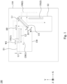
- FIG. 1 is a bottom perspective view illustrating a wireless communication device 100 according to an embodiment of the disclosure.
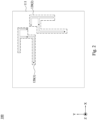
- FIG. 2 is a top view of the wireless communication device 100 according to an embodiment of the disclosure.
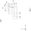
- FIG. 3 is a top view of an antenna unit in the wireless communication device 100 according to an embodiment of the disclosure.
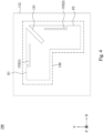
- FIG. 4 is a bottom view of the wireless communication device 100 according to an embodiment of the disclosure.
- a wireless communication device 100 includes a substrate 110, a pair of antenna units 120 (1) to 120 (2), and a metal ground 130.
- number of antenna units 120(1) to 120(2) in this embodiment is 2 and number of metal ground 130 is 1, the number of antenna units 120(1) to 120(2) can also be a positive even number more than 2 and the number of metal ground 130 can also be a positive integer more than 1. In addition, the number of antenna units 120(1) to 120(2) is twice the number of metal ground 130.
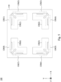
- FIG. 5 is a bottom perspective view of the wireless communication device according to another embodiment of the disclosure.
- this embodiment shows an example of one substrate 110, eight antenna units 120(1) to 120(8), and four metal ground 130(1) to 130(4).
- the substrate 110 includes a first surface 111 and a second surface 112 corresponding to each other, where the first surface 111 is shown in FIG. 2 , and the second surface 112 is shown in FIG. 4 .
- the antenna units 120(1) to 120(2) are disposed on the first surface 111, and the metal ground 130 is disposed on the second surface 112.
- FIG. 3 further illustrates the detailed structure of the antenna unit 120(1).
- the substrate 110 is a printed circuit board (PCB) made of an insulating material, where material of the substrate 110 is Teflon (PTFE) or epoxy resin (FR4), which is commonly used to manufacture PCBs.
- PCB printed circuit board
- PTFE Teflon
- FR4 epoxy resin
- the antenna units 120(1) to 120(2) is perpendicular to each other, and the antenna unit 120(1) includes a radiation part 121, a feeding part 122, a ground via 123 and a feeding line 124, where the feeding line 124 includes a first transmission line 1241 and a second transmission line 1242 that are perpendicular to each other and connected to each other, and the first transmission line 1241 is connected to the radiation part 121 via the feeding part 122.
- the feeding line 124 further includes a feeding point 1243, and the antenna unit 120(1) receives feeding signal from signal source through the feeding point 1243.
- the antenna unit 120(2) also have the same structure as the antenna unit 120(1), therefore, it will not be repeated here.
- polarization direction of the antenna unit 120(1) is y direction
- polarization direction of the antenna unit 120(2) is x direction. Accordingly, isolation of the antenna units 120(1) to 120(2) can be greatly improved (e.g., the isolation can be reduced to about -10dB).
- the antenna units 120(1) to 120(2) are planar inverted-F antennas (PIFA) with an inverted F shape.
- the antenna units 120(1) to 120(2) also can be other types of antennas (e.g., monopole antennas) having the above-mentioned feeding line structure, and the antenna units 120(1) to 120(2) can also be different types of antennas with the above-mentioned feeding line structure (e.g., the antenna unit 120(1) is a PIFA antenna, and the antenna unit 120(2) is a monopole antenna).
- the antenna units 120(1) to 120(2) are all PIFA antennas, such that the radiation part 121 of the antenna unit 120(1) includes a first radiation part 1211, a second radiation part 1212, and a third radiation part 1213, where the third radiation part 1213 is L shape.
- a first terminal of the first radiation part 1211 is connected between the second radiation part 1212 and the third radiation part 1213, and the second terminal of the first radiation part 1211 is connected to the feeding part 122.
- the third radiation part 1213 is connected to the ground via 123, and the ground via 123 is connected to the metal ground 130.
- the metal ground 130 is an inverted L shape, and the metal ground 130 is made of a metal material such as copper foil, etc..
- isolation slot 131 of the metal ground 130 is disposed on the metal ground 130, and its position respectively corresponds between projections of the antenna units 120(1) to 120(2) toward the metal ground 130, where number of isolation slots 131 is equal to the number of the metal ground 130.
- the isolation slot 131 is rectangular, and distance D1 between the isolation slot 131 and the projection of the antenna unit 120(1) to 120(2) toward the metal ground 130 is more than 1 mm.
- width W1 of the isolation slot 131 is 3.6 mm, and length L1 of the isolation slot 131 is a quarter wavelength of center frequency of an operating frequency band of the antenna units 120(1) to 120(2).
- the wavelength of the center frequency of the operating frequency band of the antenna units 120(1) to 120(2) is affected by the material of the substrate 110 (i.e., different materials correspond to different wavelengths).
- the wavelength of the center frequency of the operating frequency band of the antenna unit 120(1) to 120(2) is mainly related to the effective dielectric constant (Dkeff) of the material of the substrate 110 (i.e., approximately value obtained by adding 1 to a dielectric constant (Dk) and dividing by 2).
- Dkeff effective dielectric constant
- the dielectric constant of Teflon is 3.0 to 4.5
- the dielectric constant of FR4 is 3.5.
- an equivalent value is obtained from square root of the above-mentioned effective dielectric constant, and the wavelength of the center frequency of the operating frequency band of the antenna unit 120(1) to 120(2) is inversely proportional to the equivalent value.
- the antenna unit 120(1) to 120(2) will resonate with the isolation slot 131 to block the signal generated by the antenna unit 120(1) to 120(2), thereby greatly increasing the isolation of the antenna unit 120(1) to 120(2) (i.e., the isolation is further reduced to below -20dB).
- FIG. 6 is an s-parameter of isolation and frequency of two antenna units according to another embodiment of the disclosure.
- the isolation of the antenna units 120(1) to 120(2) is obviously reduced to below -20dB.
- the isolation of the antenna units 120(1) to 120(2) can fulfill isolation requirement of the 5G new radio (5G NR) standard (i.e., less than -20dB).
- 5G NR 5G new radio
- the metal ground 130 has edges E1 to E2, where the edges E1 to E2 are perpendicular to each other, and the edges E1 to E2 are perpendicular to projections of the radiating parts of the antenna units 120(1) to 120(2) toward the metal ground 130, respectively.
- edge E1 is perpendicular to a projection of a part of the radiation part 121 nearby the feeding part 122 toward the metal ground 130.
- edge E2 also can be disposed in a similar manner.
- length of the edges E1 to E2 is a half wavelength of the center frequency of the operating frequency band of the antenna units 120(1) to 120(2).
- the resonance slots 132(1) to 132(2) are disposed on the metal ground 130, and their positions correspond to projections of second transmission lines of the feeding lines in the antenna units 120(1) to 120(2) toward the metal ground 130 and the corresponding one of the edges E1 to E2.
- the position of the resonance slot 132(1) is between the projection of the second transmission line 1242 of the feeding line 124 toward the metal ground 130 and the edge E1.
- the position of the resonance slot 132(2) also can be disposed in a similar manner.
- the shape of the resonance slots 132(1) to 132(2) is L shape, and length of the resonance slot 132(1) to 132(2) (i.e., sum of length L2 and the length L3) is the quarter wavelength of the center frequency of the operating frequency band of the antenna units 120(1) to 120(2).
- width W2 of the resonance slot 132(1) to 132(2) is 1mm
- distance D2 between the resonance slots 132(1) to 132(2) and projections of the antenna units 120(1) to 120(2) toward the metal ground 130 is more than 1 mm.
- the distance D2 between the resonance slot 132(1) and the projection of the feeding part 122 of the antenna unit 120(1) toward the metal ground 130 is more than 1 mm.
- the resonance slot 132(2) also can be disposed in a similar manner.
- the radiation parts of the antenna units 120(1) to 120(2) (e.g., the radiation part 121 of the antenna unit 120(1)) resonate by themselves to generate a first resonance frequency band
- the resonance slots 132(1) to 132(2) respectively resonate with the radiation parts of the antenna units 120(1) to 120(2) to generate a second resonance frequency band adjacent to the first resonance frequency band, where the operating frequency bands of the antenna units 120(1) to 120(2) includes the first resonance frequency band and the second resonance frequency band.
- the operating frequency band of the antenna units 120(1) to 120(2) is greatly increased.
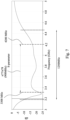
- FIG. 7 is an s-parameter (return loss) of operating frequency bands of the two antenna units according to another embodiment of the disclosure.
- frequency band n77/n78 of the general fifth-generation new radio (5G NR) standard is 3.3 GHz to 4.2 GHz (bandwidth is 900 MHz).
- the operating frequency band of the antenna units 120(1) to 120(2) is 3.19 GHz to 4.46 GHz (return loss is less than -10dB).
- the operating frequency bands of the antenna units 120(1) to 120(2) can simultaneously fulfill the frequency bands n77/n78 of the 5G NR standard.
- the antenna unit 120(1), the resonance slot 132(1), a part of the substrate 110 and a part of the metal ground 130 can form a resonance structure.
- the antenna unit 120(2), the resonance slot 132(2), another part of the substrate 110, and another part of the metal ground 130 can also form another resonance structure.
- the above-mentioned antenna structure can be used to further fulfill the high operating bandwidth of the 5G NR standard and the high isolation of the antenna unit in the sub-7 GHz frequency band.
- the wireless communication device provided by the present disclosure utilizes the isolation slots between adjacent antenna units and the vertical disposing of the antenna units to greatly increase the isolation of the antenna units.
- the wireless communication device provided by the present disclosure further utilizes the resonance slot of the feeding line adjacent to the antenna unit, which greatly increases the operating bandwidth of the antenna unit. Accordingly, it can fulfill the high operating bandwidth of the 5G NR standard and the high isolation of the antenna unit in the sub-7 GHz frequency band.
Landscapes
- Physics & Mathematics (AREA)
- Electromagnetism (AREA)
- Variable-Direction Aerials And Aerial Arrays (AREA)
- Waveguide Aerials (AREA)
- Details Of Aerials (AREA)
Claims (6)
- Drahtloses Kommunikationsgerät (100), mit:einem Substrat (110), das eine erste Oberfläche (111) und eine zweite Oberfläche (112) aufweist;einer Antennenstruktur, die eine erste Antenneneinheit (120(1)) und eine zweite Antenneneinheit (120(2)) aufweist, die auf der ersten Oberfläche (111) angeordnet sind und senkrecht zueinander stehen, wobei jede der ersten und zweiten Antenneneinheiten (120(1) und 120(2)) ein erstes Strahlungsteil (1211), ein zweites Strahlungsteil (1212), ein drittes Strahlungsteil (1213), ein Einspeiseteil (122) und eine Einspeiseleitung (124) aufweist, unddie Einspeiseleitung (124) eine erste Übertragungsleitung (1241) und eine zweite Übertragungsleitung (1242) aufweist, die senkrecht zueinander verlaufen und miteinander verbunden sind, wobei die erste Übertragungsleitung (1241) der Einspeiseleitung (124) mit dem ersten Strahlungsteil (1211) über das Einspeiseteil (122) verbunden ist; undeiner Metallmasse (130), die auf der zweiten Oberfläche (112) angeordnet ist, wobei ein Isolationsschlitz (131) auf der Metallmasse (130) angeordnet ist, wobei diese Anordnung einer Position zwischen den Vorsprüngen der ersten und zweiten Antenneneinheiten (120(1) und 120(2)) in Richtung auf die Metallmasse (130) entspricht,die Metallmasse (130) einen ersten Rand (E1) und einen zweiten Rand (E2) aufweist, wobei die beiden Ränder (E1 und E2) senkrecht zueinander stehen und der erste Rand (E1) senkrecht zu Vorsprüngen des ersten Strahlungsteils (1211) und eines Abschnittes des dritten Teils des Strahlungsteils (1213) der ersten Antenneneinheit (120(1)) in Richtung auf die Metallmasse (130) und parallel zu Vorsprüngen des zweiten Strahlungsteils (1212) und eines anderen Abschnittes des dritten Strahlungsteils (1213) der ersten Antenneneinheit (120(1)) in Richtung auf die Metallmasse (130) verläuft,der zweite Rand (E2) senkrecht zu Vorsprüngen des ersten Strahlungsteils (1211) und eines Abschnitts des dritten Strahlungsteils (1213) der zweiten Antenneneinheit (120(2)) in Richtung auf die Metallmasse (130) und parallel zu Vorsprüngen des zweiten Strahlungsteils (1212) und eines anderen Abschnitts des dritten Strahlungsteils (1213) der zweiten Antenneneinheit (120(2)) in Richtung auf die Metallmasse (130) verläuft; undeinem ersten Resonanzschlitz (132(1)) und einem zweiten Resonanzschlitz (132(2)), wobei der erste Resonanzschlitz (132(1)) zwischen dem ersten Rand (E1) und einem Vorsprung der zweiten Übertragungsleitung (1242) der Einspeiseleitung (124) der ersten Antenneneinheit (120(1)) in Richtung auf die Metallmasse (130) angeordnet ist, undwobei der zweite Resonanzschlitz (132(2)) zwischen dem zweiten Rand (E2) und einem Vorsprung der zweiten Übertragungsleitung (1242) der Einspeiseleitung (124) der zweiten Antenneneinheit (120(2)) in Richtung auf die Metallmasse (130) angeordnet ist,wobei die ersten und zweiten Resonanzschlitze (132(1) und 132(2)) L-förmig sind.
- Drahtloses Kommunikationsgerät (100) nach Anspruch 1,
wobei der Isolationsschlitz (131) rechteckig ist, wobei eine Länge des Isolationsschlitzes (131) und eine Länge der zwei Resonanzschlitze (132(1) und 132(2)) eine Viertelwellenlänge der Mittenfrequenz eines Betriebsfrequenzbandes der zwei Antenneneinheiten (120(1) und 120(2)) beträgt und eine Länge der zwei Ränder (E1 und E2) eine halbe Wellenlänge der Mittenfrequenz des Betriebsfrequenzbandes der zwei Antenneneinheiten (120(1) und 120(2)) beträgt. - Drahtloses Kommunikationsgerät (100) nach Anspruch 1,
bei welchem eine Breite des Isolationsschlitzes (131) 3,6 mm beträgt und eine Breite der zwei Resonanzschlitze (132(1) und 132(2)) 1 mm beträgt, wobei ein Abstand zwischen dem Isolationsschlitz (131) und einem Vorsprung der ersten Antenneneinheit (120(1)) oder der zweiten Antenneneinheit (120(2)) in Richtung auf die Metallmasse (130) mehr als 1 mm beträgt. - Drahtloses Kommunikationsgerät (100) nach Anspruch 1,
bei welchem das erste Strahlungsteil (1211), das zweite Strahlungsteil (1212) und das dritte Strahlungsteil (1213) mit sich selbst in Resonanz treten, um ein erstes Resonanzfrequenzband zu erzeugen, und die zwei Resonanzschlitze (132(1) und 132(2)) jeweils mit dem ersten Strahlungsteil (1211), dem zweiten Strahlungsteil (1212) und dem dritten Strahlungsteil (1213) in Resonanz treten, um ein zweites Resonanzfrequenzband neben dem ersten Resonanzfrequenzband zu erzeugen. - Drahtloses Kommunikationsgerät (100) nach Anspruch 1,
wobei das erste Strahlungsteil (1211), das zweite Strahlungsteil (1212) und das dritte Strahlungsteil (1213) eine umgekehrte F-Form bilden und die Einspeiseleitung (124) eine L-Form hat, wobei der Isolationsschlitz (131) so konfiguriert ist, dass er die Signalübertragung zwischen den beiden Antenneneinheiten (120(1) und 120(2)) blockiert, um die Isolation der beiden Antenneneinheiten (120(1) und 120(2)) zu erhöhen. - Drahtloses Kommunikationsgerät (100) nach Anspruch 1, das eine Vielzahl von Antennenstrukturen aufweist.
Applications Claiming Priority (1)
| Application Number | Priority Date | Filing Date | Title |
|---|---|---|---|
| CN202110411522.0A CN115224482B (zh) | 2021-04-16 | 2021-04-16 | 天线结构以及无线通信装置 |
Publications (3)
| Publication Number | Publication Date |
|---|---|
| EP4075601A1 EP4075601A1 (de) | 2022-10-19 |
| EP4075601B1 true EP4075601B1 (de) | 2024-09-25 |
| EP4075601C0 EP4075601C0 (de) | 2024-09-25 |
Family
ID=78483211
Family Applications (1)
| Application Number | Title | Priority Date | Filing Date |
|---|---|---|---|
| EP21205774.9A Active EP4075601B1 (de) | 2021-04-16 | 2021-11-01 | Antennenstruktur und drahtlose kommunikationsvorrichtung |
Country Status (6)
| Country | Link |
|---|---|
| US (1) | US11916293B2 (de) |
| EP (1) | EP4075601B1 (de) |
| JP (1) | JP7384533B2 (de) |
| CN (1) | CN115224482B (de) |
| ES (1) | ES3000136T3 (de) |
| PL (1) | PL4075601T3 (de) |
Families Citing this family (3)
| Publication number | Priority date | Publication date | Assignee | Title |
|---|---|---|---|---|
| CN118487027A (zh) * | 2023-02-10 | 2024-08-13 | 台达电子工业股份有限公司 | 天线结构以及天线装置 |
| TWI851207B (zh) * | 2023-05-16 | 2024-08-01 | 智易科技股份有限公司 | 可增加隔離度的天線結構 |
| CN220914575U (zh) * | 2023-09-21 | 2024-05-07 | 智邦科技股份有限公司 | 天线模块 |
Family Cites Families (16)
| Publication number | Priority date | Publication date | Assignee | Title |
|---|---|---|---|---|
| US7162538B1 (en) | 2000-10-04 | 2007-01-09 | Intel Corporation | Peer to peer software distribution system |
| US6624790B1 (en) * | 2002-05-08 | 2003-09-23 | Accton Technology Corporation | Integrated dual-band printed monopole antenna |
| JP2006115182A (ja) * | 2004-10-14 | 2006-04-27 | Alps Electric Co Ltd | パターンアンテナ |
| FR2942676A1 (fr) * | 2009-02-27 | 2010-09-03 | Thomson Licensing | Systeme d'antennes compact a diversite d'ordre 2. |
| US20120214424A1 (en) | 2011-02-23 | 2012-08-23 | Mediatek Inc. | Single Input/Multiple Output (SIMO) or Multiple Input/Single Output (MISO) or Multiple Input/Multiple Output (MIMO) Antenna Module |
| TWI483464B (zh) * | 2011-10-20 | 2015-05-01 | Acer Inc | 通訊裝置及其天線結構 |
| JP5919921B2 (ja) * | 2012-03-19 | 2016-05-18 | 富士通株式会社 | アンテナ装置及び電子装置 |
| EP2830154A4 (de) * | 2012-03-22 | 2015-11-11 | Nec Corp | Antennenvorrichtung und drahtloses endgerät damit |
| TWI568076B (zh) * | 2014-03-17 | 2017-01-21 | 廣達電腦股份有限公司 | 天線結構 |
| TWI559613B (zh) * | 2015-09-22 | 2016-11-21 | 智易科技股份有限公司 | 高隔離度之多天線結構 |
| TWM537316U (zh) * | 2016-01-14 | 2017-02-21 | 啓碁科技股份有限公司 | 天線結構 |
| TWI648908B (zh) | 2017-05-09 | 2019-01-21 | 和碩聯合科技股份有限公司 | 電子裝置與其天線結構 |
| US10424832B2 (en) | 2017-10-20 | 2019-09-24 | Elements of Genius, Inc. | Wearable device antenna apparatus and system |
| CN110635229A (zh) | 2018-06-22 | 2019-12-31 | 启碁科技股份有限公司 | 天线结构 |
| TWI679799B (zh) | 2018-08-28 | 2019-12-11 | 啓碁科技股份有限公司 | 行動裝置 |
| TWI704716B (zh) * | 2019-07-05 | 2020-09-11 | 宏碁股份有限公司 | 行動裝置 |
-
2021
- 2021-04-16 CN CN202110411522.0A patent/CN115224482B/zh active Active
- 2021-10-08 JP JP2021166381A patent/JP7384533B2/ja active Active
- 2021-10-11 US US17/450,556 patent/US11916293B2/en active Active
- 2021-11-01 EP EP21205774.9A patent/EP4075601B1/de active Active
- 2021-11-01 ES ES21205774T patent/ES3000136T3/es active Active
- 2021-11-01 PL PL21205774.9T patent/PL4075601T3/pl unknown
Also Published As
| Publication number | Publication date |
|---|---|
| PL4075601T3 (pl) | 2025-03-17 |
| EP4075601A1 (de) | 2022-10-19 |
| JP7384533B2 (ja) | 2023-11-21 |
| US20220336958A1 (en) | 2022-10-20 |
| CN115224482B (zh) | 2025-07-25 |
| CN115224482A (zh) | 2022-10-21 |
| JP2022164538A (ja) | 2022-10-27 |
| EP4075601C0 (de) | 2024-09-25 |
| ES3000136T3 (en) | 2025-02-27 |
| US11916293B2 (en) | 2024-02-27 |
Similar Documents
| Publication | Publication Date | Title |
|---|---|---|
| Rafique et al. | Dual-band microstrip patch antenna array for 5G mobile communications | |
| EP2919323A1 (de) | Gruppenantenne | |
| EP4075601B1 (de) | Antennenstruktur und drahtlose kommunikationsvorrichtung | |
| US20190305415A1 (en) | Integrated multi-standard antenna system with dual function connected array | |
| KR20030090716A (ko) | 이중 대역 패치 및 나비넥타이형 슬롯 안테나 구조 | |
| CN110783704B (zh) | 双过孔探针馈电集成基片间隙波导圆极化天线 | |
| US8648762B2 (en) | Loop array antenna system and electronic apparatus having the same | |
| US11456526B2 (en) | Antenna unit, antenna system and electronic device | |
| US12278435B2 (en) | Miniature antenna with omnidirectional radiation field | |
| US20110291902A1 (en) | Wideband l-shaped circular polarized monopole slot antenna | |
| CN116868442A (zh) | 包括耦合谐振结构层的低剖面设备 | |
| US7911390B2 (en) | Antenna structure | |
| US11011833B2 (en) | Antenna structure and electronic device | |
| US12191574B2 (en) | Antenna array device | |
| US20210159586A1 (en) | Antenna structure | |
| US11721908B2 (en) | Antenna structure with wide beamwidth | |
| TWI763439B (zh) | 天線結構以及無線通訊裝置 | |
| Hamid et al. | Wideband reconfigurable log periodic patch array | |
| Chen et al. | Mutual coupling reduction of slot array antenna for 5G millimeter-wave handset | |
| CN112993575A (zh) | 一种WiFi全向天线 | |
| Algburi et al. | A Dual Band Monopole Antenna with Slots for Wireless Applications | |
| CN219833013U (zh) | 一种宽带串馈低副瓣微带阵列结构 | |
| Nataraj et al. | Analysis and design of microstrip antenna array for S-band applications | |
| US20250055189A1 (en) | Compact dual polarity radiator for a dense array | |
| Zalki | Dual Band Microstrip Patch Antenna For Wireless Communication Applications |
Legal Events
| Date | Code | Title | Description |
|---|---|---|---|
| PUAI | Public reference made under article 153(3) epc to a published international application that has entered the european phase |
Free format text: ORIGINAL CODE: 0009012 |
|
| STAA | Information on the status of an ep patent application or granted ep patent |
Free format text: STATUS: THE APPLICATION HAS BEEN PUBLISHED |
|
| AK | Designated contracting states |
Kind code of ref document: A1 Designated state(s): AL AT BE BG CH CY CZ DE DK EE ES FI FR GB GR HR HU IE IS IT LI LT LU LV MC MK MT NL NO PL PT RO RS SE SI SK SM TR |
|
| STAA | Information on the status of an ep patent application or granted ep patent |
Free format text: STATUS: REQUEST FOR EXAMINATION WAS MADE |
|
| 17P | Request for examination filed |
Effective date: 20230227 |
|
| RBV | Designated contracting states (corrected) |
Designated state(s): AL AT BE BG CH CY CZ DE DK EE ES FI FR GB GR HR HU IE IS IT LI LT LU LV MC MK MT NL NO PL PT RO RS SE SI SK SM TR |
|
| RIC1 | Information provided on ipc code assigned before grant |
Ipc: H01Q 1/48 20060101ALN20240328BHEP Ipc: H01Q 21/28 20060101ALI20240328BHEP Ipc: H01Q 1/52 20060101ALI20240328BHEP Ipc: H01Q 13/10 20060101ALI20240328BHEP Ipc: H01Q 5/40 20150101ALI20240328BHEP Ipc: H01Q 9/42 20060101AFI20240328BHEP |
|
| GRAP | Despatch of communication of intention to grant a patent |
Free format text: ORIGINAL CODE: EPIDOSNIGR1 |
|
| STAA | Information on the status of an ep patent application or granted ep patent |
Free format text: STATUS: GRANT OF PATENT IS INTENDED |
|
| INTG | Intention to grant announced |
Effective date: 20240514 |
|
| GRAS | Grant fee paid |
Free format text: ORIGINAL CODE: EPIDOSNIGR3 |
|
| GRAA | (expected) grant |
Free format text: ORIGINAL CODE: 0009210 |
|
| STAA | Information on the status of an ep patent application or granted ep patent |
Free format text: STATUS: THE PATENT HAS BEEN GRANTED |
|
| AK | Designated contracting states |
Kind code of ref document: B1 Designated state(s): AL AT BE BG CH CY CZ DE DK EE ES FI FR GB GR HR HU IE IS IT LI LT LU LV MC MK MT NL NO PL PT RO RS SE SI SK SM TR |
|
| REG | Reference to a national code |
Ref country code: GB Ref legal event code: FG4D |
|
| REG | Reference to a national code |
Ref country code: CH Ref legal event code: EP |
|
| REG | Reference to a national code |
Ref country code: DE Ref legal event code: R096 Ref document number: 602021019239 Country of ref document: DE |
|
| REG | Reference to a national code |
Ref country code: IE Ref legal event code: FG4D |
|
| U01 | Request for unitary effect filed |
Effective date: 20241017 |
|
| U07 | Unitary effect registered |
Designated state(s): AT BE BG DE DK EE FI FR IT LT LU LV MT NL PT RO SE SI Effective date: 20241104 |
|
| U20 | Renewal fee for the european patent with unitary effect paid |
Year of fee payment: 4 Effective date: 20241106 |
|
| PG25 | Lapsed in a contracting state [announced via postgrant information from national office to epo] |
Ref country code: NO Free format text: LAPSE BECAUSE OF FAILURE TO SUBMIT A TRANSLATION OF THE DESCRIPTION OR TO PAY THE FEE WITHIN THE PRESCRIBED TIME-LIMIT Effective date: 20241225 |
|
| PG25 | Lapsed in a contracting state [announced via postgrant information from national office to epo] |
Ref country code: GR Free format text: LAPSE BECAUSE OF FAILURE TO SUBMIT A TRANSLATION OF THE DESCRIPTION OR TO PAY THE FEE WITHIN THE PRESCRIBED TIME-LIMIT Effective date: 20241226 |
|
| PG25 | Lapsed in a contracting state [announced via postgrant information from national office to epo] |
Ref country code: RS Free format text: LAPSE BECAUSE OF FAILURE TO SUBMIT A TRANSLATION OF THE DESCRIPTION OR TO PAY THE FEE WITHIN THE PRESCRIBED TIME-LIMIT Effective date: 20241225 |
|
| PG25 | Lapsed in a contracting state [announced via postgrant information from national office to epo] |
Ref country code: RS Free format text: LAPSE BECAUSE OF FAILURE TO SUBMIT A TRANSLATION OF THE DESCRIPTION OR TO PAY THE FEE WITHIN THE PRESCRIBED TIME-LIMIT Effective date: 20241225 Ref country code: NO Free format text: LAPSE BECAUSE OF FAILURE TO SUBMIT A TRANSLATION OF THE DESCRIPTION OR TO PAY THE FEE WITHIN THE PRESCRIBED TIME-LIMIT Effective date: 20241225 Ref country code: GR Free format text: LAPSE BECAUSE OF FAILURE TO SUBMIT A TRANSLATION OF THE DESCRIPTION OR TO PAY THE FEE WITHIN THE PRESCRIBED TIME-LIMIT Effective date: 20241226 |
|
| REG | Reference to a national code |
Ref country code: ES Ref legal event code: FG2A Ref document number: 3000136 Country of ref document: ES Kind code of ref document: T3 Effective date: 20250227 |
|
| PG25 | Lapsed in a contracting state [announced via postgrant information from national office to epo] |
Ref country code: IS Free format text: LAPSE BECAUSE OF FAILURE TO SUBMIT A TRANSLATION OF THE DESCRIPTION OR TO PAY THE FEE WITHIN THE PRESCRIBED TIME-LIMIT Effective date: 20250125 |
|
| PG25 | Lapsed in a contracting state [announced via postgrant information from national office to epo] |
Ref country code: SM Free format text: LAPSE BECAUSE OF FAILURE TO SUBMIT A TRANSLATION OF THE DESCRIPTION OR TO PAY THE FEE WITHIN THE PRESCRIBED TIME-LIMIT Effective date: 20240925 |
|
| PG25 | Lapsed in a contracting state [announced via postgrant information from national office to epo] |
Ref country code: CZ Free format text: LAPSE BECAUSE OF FAILURE TO SUBMIT A TRANSLATION OF THE DESCRIPTION OR TO PAY THE FEE WITHIN THE PRESCRIBED TIME-LIMIT Effective date: 20240925 |
|
| PG25 | Lapsed in a contracting state [announced via postgrant information from national office to epo] |
Ref country code: SK Free format text: LAPSE BECAUSE OF FAILURE TO SUBMIT A TRANSLATION OF THE DESCRIPTION OR TO PAY THE FEE WITHIN THE PRESCRIBED TIME-LIMIT Effective date: 20240925 |
|
| REG | Reference to a national code |
Ref country code: CH Ref legal event code: PL |
|
| PG25 | Lapsed in a contracting state [announced via postgrant information from national office to epo] |
Ref country code: MC Free format text: LAPSE BECAUSE OF FAILURE TO SUBMIT A TRANSLATION OF THE DESCRIPTION OR TO PAY THE FEE WITHIN THE PRESCRIBED TIME-LIMIT Effective date: 20240925 |
|
| REG | Reference to a national code |
Ref country code: CH Ref legal event code: PL |
|
| PG25 | Lapsed in a contracting state [announced via postgrant information from national office to epo] |
Ref country code: CH Free format text: LAPSE BECAUSE OF NON-PAYMENT OF DUE FEES Effective date: 20241130 |
|
| PLBE | No opposition filed within time limit |
Free format text: ORIGINAL CODE: 0009261 |
|
| STAA | Information on the status of an ep patent application or granted ep patent |
Free format text: STATUS: NO OPPOSITION FILED WITHIN TIME LIMIT |
|
| 26N | No opposition filed |
Effective date: 20250626 |
|
| PGFP | Annual fee paid to national office [announced via postgrant information from national office to epo] |
Ref country code: PL Payment date: 20250827 Year of fee payment: 5 |
|
| PGFP | Annual fee paid to national office [announced via postgrant information from national office to epo] |
Ref country code: GB Payment date: 20250911 Year of fee payment: 5 |
|
| PG25 | Lapsed in a contracting state [announced via postgrant information from national office to epo] |
Ref country code: IE Free format text: LAPSE BECAUSE OF NON-PAYMENT OF DUE FEES Effective date: 20241101 |
|
| U20 | Renewal fee for the european patent with unitary effect paid |
Year of fee payment: 5 Effective date: 20251008 |
|
| PG25 | Lapsed in a contracting state [announced via postgrant information from national office to epo] |
Ref country code: HR Free format text: LAPSE BECAUSE OF FAILURE TO SUBMIT A TRANSLATION OF THE DESCRIPTION OR TO PAY THE FEE WITHIN THE PRESCRIBED TIME-LIMIT Effective date: 20240925 |
|
| PGFP | Annual fee paid to national office [announced via postgrant information from national office to epo] |
Ref country code: ES Payment date: 20251212 Year of fee payment: 5 |