EP4075152A1 - Phasengesteuerte antennenvorrichtung - Google Patents
Phasengesteuerte antennenvorrichtung Download PDFInfo
- Publication number
- EP4075152A1 EP4075152A1 EP20899133.1A EP20899133A EP4075152A1 EP 4075152 A1 EP4075152 A1 EP 4075152A1 EP 20899133 A EP20899133 A EP 20899133A EP 4075152 A1 EP4075152 A1 EP 4075152A1
- Authority
- EP
- European Patent Office
- Prior art keywords
- antenna element
- row
- fft
- column
- converter
- Prior art date
- Legal status (The legal status is an assumption and is not a legal conclusion. Google has not performed a legal analysis and makes no representation as to the accuracy of the status listed.)
- Granted
Links
Images





Classifications
-
- H—ELECTRICITY
- H01—ELECTRIC ELEMENTS
- H01Q—ANTENNAS, i.e. RADIO AERIALS
- H01Q13/00—Waveguide horns or mouths; Slot antennas; Leaky-waveguide antennas; Equivalent structures causing radiation along the transmission path of a guided wave
- H01Q13/02—Waveguide horns
- H01Q13/0275—Ridged horns
-
- G—PHYSICS
- G01—MEASURING; TESTING
- G01R—MEASURING ELECTRIC VARIABLES; MEASURING MAGNETIC VARIABLES
- G01R29/00—Arrangements for measuring or indicating electric quantities not covered by groups G01R19/00 - G01R27/00
- G01R29/08—Measuring electromagnetic field characteristics
-
- G—PHYSICS
- G01—MEASURING; TESTING
- G01S—RADIO DIRECTION-FINDING; RADIO NAVIGATION; DETERMINING DISTANCE OR VELOCITY BY USE OF RADIO WAVES; LOCATING OR PRESENCE-DETECTING BY USE OF THE REFLECTION OR RERADIATION OF RADIO WAVES; ANALOGOUS ARRANGEMENTS USING OTHER WAVES
- G01S7/00—Details of systems according to groups G01S13/00, G01S15/00, G01S17/00
- G01S7/02—Details of systems according to groups G01S13/00, G01S15/00, G01S17/00 of systems according to group G01S13/00
- G01S7/03—Details of HF subsystems specially adapted therefor, e.g. common to transmitter and receiver
-
- H—ELECTRICITY
- H01—ELECTRIC ELEMENTS
- H01Q—ANTENNAS, i.e. RADIO AERIALS
- H01Q3/00—Arrangements for changing or varying the orientation or the shape of the directional pattern of the waves radiated from an antenna or antenna system
- H01Q3/26—Arrangements for changing or varying the orientation or the shape of the directional pattern of the waves radiated from an antenna or antenna system varying the relative phase or relative amplitude of energisation between two or more active radiating elements; varying the distribution of energy across a radiating aperture
- H01Q3/2682—Time delay steered arrays
-
- G—PHYSICS
- G01—MEASURING; TESTING
- G01R—MEASURING ELECTRIC VARIABLES; MEASURING MAGNETIC VARIABLES
- G01R29/00—Arrangements for measuring or indicating electric quantities not covered by groups G01R19/00 - G01R27/00
- G01R29/08—Measuring electromagnetic field characteristics
- G01R29/0864—Measuring electromagnetic field characteristics characterised by constructional or functional features
- G01R29/0878—Sensors; antennas; probes; detectors
-
- G—PHYSICS
- G01—MEASURING; TESTING
- G01S—RADIO DIRECTION-FINDING; RADIO NAVIGATION; DETERMINING DISTANCE OR VELOCITY BY USE OF RADIO WAVES; LOCATING OR PRESENCE-DETECTING BY USE OF THE REFLECTION OR RERADIATION OF RADIO WAVES; ANALOGOUS ARRANGEMENTS USING OTHER WAVES
- G01S13/00—Systems using the reflection or reradiation of radio waves, e.g. radar systems; Analogous systems using reflection or reradiation of waves whose nature or wavelength is irrelevant or unspecified
- G01S13/02—Systems using reflection of radio waves, e.g. primary radar systems; Analogous systems
- G01S2013/0236—Special technical features
- G01S2013/0245—Radar with phased array antenna
- G01S2013/0263—Passive array antenna
-
- Y—GENERAL TAGGING OF NEW TECHNOLOGICAL DEVELOPMENTS; GENERAL TAGGING OF CROSS-SECTIONAL TECHNOLOGIES SPANNING OVER SEVERAL SECTIONS OF THE IPC; TECHNICAL SUBJECTS COVERED BY FORMER USPC CROSS-REFERENCE ART COLLECTIONS [XRACs] AND DIGESTS
- Y02—TECHNOLOGIES OR APPLICATIONS FOR MITIGATION OR ADAPTATION AGAINST CLIMATE CHANGE
- Y02A—TECHNOLOGIES FOR ADAPTATION TO CLIMATE CHANGE
- Y02A90/00—Technologies having an indirect contribution to adaptation to climate change
- Y02A90/10—Information and communication technologies [ICT] supporting adaptation to climate change, e.g. for weather forecasting or climate simulation
Definitions
- the present invention mainly relates to a phased-array antenna device that receives microwaves.
- a microwave radiometer is a radiometer that passively observes the intensity of extremely weak electromagnetic waves in a microwave range radiated from the ground surface for each frequency component.
- An object radiates weak electromagnetic waves by blackbody radiation based on its temperature.
- the microwave radiometer detects the intensity of weak electromagnetic waves based on the blackbody radiation using time integration.
- Non-Patent Literature 1 The applicant operates an artificial satellite equipped with a microwave radiometer disclosed in Non-Patent Literature 1 to observe the temperature of the sea surface, the salinity concentration of seawater, measurement of soil moisture, and the like from the observed luminance temperature.
- Patent Literature 1 discloses the technical details of an electronic scanning microwave radiometer that enables single-area scanning of the earth surface or the like at a conical and a predetermined fixed incident angle.
- Non-Patent Literature 2 discloses the technical details related to a combination of numbers that reduces the redundancy of antenna elements of a phased array antenna.
- Patent Literature 1 JP H7-209359 A
- the microwave radiometer disclosed in Non-Patent Literature 1 and mounted on an artificial satellite currently in operation is equipped with a horn antenna for each of a plurality of frequency bands, and rotationally drives a disk-shaped reflecting mirror at a speed of one rotation every 1.5 seconds.
- the rotating part including the reflecting mirror weighs about 250 kg.
- the current microwave radiometer disclosed in Non-Patent Literature 1 has the following problems.
- a purpose of the present invention is to provide a phased-array antenna device that solves the problems, has high spatial resolution, realizes microwave observation of a broad band and high frequency resolution, and has a long operating lifespan achieved without using a mechanically movable component.
- a phased-array antenna device in the present invention includes a first antenna element, a first preamplifier that amplifies a signal obtained from the first antenna element, a first BPF that passes only a signal in a predetermined frequency band from an output signal of the first preamplifier, and a first A/D converter that converts an output signal of the first BPF into digital data.
- the phased-array antenna device in the present invention includes a first FFT that performs a Fourier transform on data output from the first A/D converter, a second antenna element arranged apart from the first antenna element by a predetermined distance, a second preamplifier that amplifies a signal obtained from the second antenna element, and a second BPF that passes only a signal in the same frequency band as the first BPF from an output signal of the second preamplifier.
- the phased-array antenna device in the present invention includes a second A/D converter that converts an output signal of the second BPF into digital data, a second FFT that performs a Fourier transform on data output from the second A/D converter, and a first cross-spectrum calculation unit that multiplies output data of the first FFT and output data of the second FFT for the same complex frequency component after converting one of the output data of the first FFT and the output data of the second FFT into a conjugate complex number.
- the phased-array antenna device in the present invention includes a clock control unit that supplies a sampling clock whose output timing is relatively shifted to the first A/D converter and the second A/D converter.
- phased-array antenna device that has high spatial resolution, realizes microwave observation of a broad band and high frequency resolution, and has a long operating lifespan achieved without using a mechanically movable component.
- a phased array antenna that does not use a mechanically movable component disclosed in Patent Literature 1 is advantageous.
- phased-array antenna device employs these antenna elements as phased array antennas and digitizes signal processing to achieve a broader band of the phased-array antenna device.
- phased array antennas having the conventional structure cause signal processing circuits to be redundant. Therefore, the phased-array antenna device according to the embodiment of the present invention achieves a non-redundant phased-array antenna device with a minimum configuration of antenna elements and signal processing circuits by applying the technique disclosed in Non-Patent Literature 2.
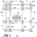
- Fig. 1 is a schematic diagram illustrating an overall configuration of a phased-array antenna device 101 according to an embodiment of the present invention.
- Antenna elements 103 and front-end units 104 are installed at the intersections of a square-shaped frame 102.
- the antenna elements 103 are installed at positions corresponding to 0th, first, fourth, and sixth intersections with intervals of a distance d.
- a first-row first-column antenna element 103a corresponding to the 0th intersection is installed.
- a first-row second-column antenna element 103b corresponding to the first intersection is installed, spaced by the distance d.
- a first-row third-column antenna element 103c corresponding to the fourth intersection is installed, spaced by a distance 3d.
- a first-row fourth-column antenna element 103d corresponding to the sixth intersection is installed, spaced by a distance 2d.
- Non-Patent Literature 2 The spacing "1-3-2" between these antenna elements 103 is disclosed in Non-Patent Literature 2.
- a second-row first-column antenna element 103e a second-row second-column antenna element 103f, a second-row third-column antenna element 103g, and a second-row fourth-column antenna element 103h are installed in the same positional relationship as in the first row described above.
- a third-row first-column antenna element 103i a third-row second-column antenna element 103j, a third-row third-column antenna element 103k, and a third-row fourth-column antenna element 1031 are installed in the same positional relationship as in the first row described above.
- a fourth-row first-column antenna element 103m a fourth-row second-column antenna element 103n, a fourth-row third-column antenna element 103o, and a fourth-row fourth-column antenna element 103p are installed in the same positional relationship as in the first row described above.
- the first-row first-column antenna element 103a and the second-row first-column antenna element 103e are spaced by the distance d in the longitudinal direction.
- the second-row first-column antenna element 103e corresponding to the first intersection is installed, spaced by the distance d.
- the second-row first-column antenna element 103e and the third-row first-column antenna element 103i are spaced by the distance 3d in the longitudinal direction.
- the third-row first-column antenna element 103i corresponding to the fourth intersection is installed, spaced by the distance 3d.
- the third-row first-column antenna element 103i and the fourth-row first-column antenna element 103m are spaced by the distance 2d in the longitudinal direction.
- the fourth-row first-column antenna element 103m corresponding to the sixth intersection is installed, spaced by the distance 2d.
- the 0th antenna element and the first antenna element are spaced by the distance d
- the first antenna element and the fourth antenna element are spaced by the distance 3d
- the fourth antenna element and the sixth antenna element are spaced by the distance 2d.
- this combination of the antenna elements 103 of "0-1-4-6" is a combination with high circuit utilization efficiency for eliminating redundancy in the final addition processing of the phased-array antenna device 101, and this combination is also disclosed in Non-Patent Literature 2.
- the spatial resolution of the antenna can be improved similarly to the diameter of the reflector of a parabola antenna.
- the distance d is limited due to the convenience of equipment to be mounted.
- the array antenna can receive a radio wave arriving from a desired narrow angular range with high sensitivity by installing the plurality of antenna elements 103 and superimposing received radio wave signals obtained from the respective antenna elements with a time difference. Conversely, at the time of transmission, the array antenna can transmit a radio wave in a desired narrow angular range with high output by giving a time difference to transmission radio wave signals output to the respective antenna elements.
- the frequency bands of the antenna elements 103 may be different. At this time, the frequency bands receivable by the entire array antenna are frequency bands receivable by all the antenna elements.
- a plurality of antenna elements 103 is provided on a straight line at equal intervals of a distance d, and the multiplication output of output signals of the antenna elements 103 or the multiplication output after integration is added. Then, this addition makes the directivity of the antenna sharper and reduces the side lobes.
- Non-Patent Literature 2 in the phased-array antenna device 101 according to the embodiment of the present invention, the combination of the antenna elements 103 is developed on the longitudinal and lateral plane in order to sharpen the antenna directivity in the two longitudinal and lateral directions and to form a point-like antenna beam.
- the combination of "0-1-4-6" is used in the phased-array antenna device 101 according to the embodiment of the present invention, but if more antenna elements 103 can be installed, it is possible to install the antenna elements 103 using the numerical sequence disclosed in Non-Patent Literature 2 similarly to the above example. For example, when five antenna elements 103 are installed, the spacing is set to "1-3-3-2", and the antenna elements 103 are arranged at "0-1-4-7-9". Then, the following combination is obtained.
- Fig. 2 illustrates an external perspective view of the antenna element 103.
- the antenna element 103 is a known quad-ridged feed horn antenna. Examples thereof include QH1400, QH4000, and the like manufactured by MVG Industries in France.
- horn antenna elements 201 each having a shape warped in a longitudinal direction and a lateral direction when viewed from the top are formed.
- the horn antenna elements 201 each having the warped shape achieve an extremely broad frequency band in the microwave range of the antenna element 103.
- the front-end unit 104 is installed immediately below each antenna element 103.
- the front-end unit 104 includes a preamplifier, a distributor, a band-pass filter, an A/D converter, and a register (see Fig. 3 ). That is, an analog signal obtained from each antenna element 103 is converted into digital data immediately below the antenna element 103.
- the digital data obtained from the register is aggregated into a data processing unit 105 installed in the center part of the frame 102.
- the data processing unit 105 is constituted by a known field-programmable gate array (FPGA).
- the data processing unit 105 outputs radio-wave intensity data for each desired frequency component.
- a clock control unit 106 is installed in the center part of the frame 102.
- the clock control unit 106 supplies a sampling clock to the A/D converter inside the front-end unit 104 arranged immediately below each antenna element 103.
- the front-end units 104 installed immediately below the respective antenna element 103 are all connected to the data processing unit 105 and the clock control unit 106.
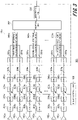
- Fig. 3 is a block diagram illustrating the overall configuration of the phased-array antenna device 101.
- the first-row first-column antenna element 103a, the first-row first-column front-end unit 104a, and a first-row first-column FFT group 301a, which is a fast Fourier transform unit inside the data processing unit 105, constitute one system of signal processing and data processing.
- first-row second-column antenna element 103b the first-row second-column front-end unit 104b, and a first-row second-column FFT group 301b constitute one system of signal processing and data processing.
- first-row third-column antenna element 103c the first-row third-column front-end unit 104c, and a first-row third-column FFT group 301c constitute one system of signal processing and data processing, and the same applies subsequently.
- the first-row fourth-column antenna element 103d, the first-row fourth-column front-end unit 104d, and a first-row fourth-column FFT group 301d constitute one system of signal processing and data processing.
- the fourth-row third-column antenna element 103o, the fourth-row third-column front-end unit 104o, and a fourth-row third-column FFT group 301o constitute one system of signal processing and data processing.
- the fourth-row fourth-column antenna element 103p, the fourth-row fourth-column front-end unit 104p, and a fourth-row fourth-column FFT group 301p constitute one system of signal processing and data processing.
- the signal output from the first-row first-column antenna element 103a is amplified by a first-row first-column preamplifier 303a (denoted as "LNA” in Fig. 3 , and the same applies to Fig. 5 ).
- the output signal of the first-row first-column preamplifier 303a is input to a first-row first-column BPF group 304a ("BPF" in Fig. 3 ), which is a band-pass filter group.
- BPF first-row first-column BPF group 304a
- Fig. 3 illustrates a single BPF, a plurality of BPFs is provided for each frequency band as described later with reference to Fig. 5 .
- a functional block for signal processing and data processing linked from a single antenna element 103 is referred to as one system in the following description. That is, the front-end unit 104 provided immediately below an antenna element 103 and the FFT group 301, which is provided inside the data processing unit 105, corresponding to the front-end unit 104 belong to one system.
- the signal output from the first-row second-column antenna element 103b is amplified by a first-row second-column preamplifier 303b.
- the output signal of the first-row second-column preamplifier 303b is input to a first-row second-column BPF group 304b.
- the output signal of the first-row third-column antenna element 103c is input to a first-row third-column BPF group 304c through a first-row third-column preamplifier 303c, and the same applies subsequently.
- the output signal of the first-row fourth-column antenna element 103d is input to a first-row fourth-column BPF group 304d through a first-row fourth-column preamplifier 303d.
- the output signal of the fourth-row third-column antenna element 103o is input to a fourth-row third-column BPF group 304o through a fourth-row third-column preamplifier 303o.
- the output signal of the fourth-row fourth-column antenna element 103p is input to a fourth-row fourth-column BPF group 304p through a fourth-row fourth-column preamplifier 303p.
- the first-row first-column preamplifier 303a to the fourth-row fourth-column preamplifier 303p are collectively referred to as a preamplifier 303, unless distinguished.
- the output signal of the first-row first-column BPF group 304a is supplied to a first-row first-column A/D converter group 305a (denoted as "ADC" in Fig. 3 , and the same applies to Fig. 5 ).
- ADC first-row first-column A/D converter group
- Fig. 3 illustrates a single A/D converter, a plurality of A/D converters is provided for each frequency band as described later with reference to Fig. 5 .
- the clock control unit 106 supplies a sampling clock to a first-row first-column A/D converter group 305a.
- the sampling clock is, for example, 16.384 GHz (16384 ⁇ 10 6 Hz).
- the sampling clock is an integral multiple of the number of a power of 2. This depends on the convenience of the subsequent FFT group 301. The reason that the sampling clock is an integral multiple of the number of a power of 2 is described later.
- the output signal of the first-row second-column BPF group 304b is supplied to a first-row second-column A/D converter group 305b.
- the output signal of the first-row third-column BPF group 304c is supplied to a first-row third-column A/D converter group 305c.
- the output signal of the first-row fourth-column BPF group 304d is supplied to a first-row fourth-column A/D converter group 305d.
- the output signal of the fourth-row third-column BPF group 304o is supplied to a fourth-row third-column A/D converter group 305o.
- the output signal of the fourth-row fourth-column BPF group 304p is supplied to a fourth-row fourth-column A/D converter group 305p.
- the first-row first-column A/D converter group 305a to the fourth-row fourth-column A/D converter group 305p are collectively referred to as an A/D converter group 305, unless distinguished.
- the sampling clock generated by the clock control unit 106 is supplied to the first-row first-column A/D converter group 305a belonging to the first-row first-column system and to the first-row second-column A/D converter group 305b belonging to the first-row second-column system.
- the clock control unit 106 gives a temporal difference to the sampling-clock supply timing according to a target direction in which the phased-array antenna device 101 receives radio waves.
- the sampling clock is relatively shifted by 2 samples between the 0th antenna element 103 and the first antenna element 103 spaced by the distance d. Between the other antenna elements 103, according to the natural number multiple of the distance, the sampling clock is shifted by the same natural number multiple.
- the data output from the first-row first-column A/D converter group 305a is stored in a first-row first-column register group 306a (denoted as "REG" in Fig. 3 ). Since the A/D converter group 305 is for the ultrahigh-speed sampling clock of 16.384 GHz, DRAMs used in general computers cannot keep up the speed, and thus the output data of the A/D converter is held by high-speed registers.
- Fig. 3 illustrates a single register, a plurality of first-row first-column register groups 306a is provided for each frequency band as described later with reference to Fig. 5 .
- the output signal of the first-row second-column A/D converter group 305b is supplied to a first-row second-column register group 306b.
- the output signal of the first-row third-column A/D converter group 305c is supplied to a first-row third-column register group 306c.
- the output signal of the first-row fourth-column A/D converter group 305d is supplied to a first-row fourth-column register group 306d.
- the output signal of the fourth-row third-column A/D converter group 305o is supplied to a fourth-row third-column register group 306o.
- the output signal of the fourth-row fourth-column A/D converter group 305p is supplied to a fourth-row fourth-column register group 306p.
- the first-row first-column register group 306a to the fourth-row fourth-column register group 306p are collectively referred to as a register group 306, unless distinguished.
- the data output from the first-row first-column register group 306a is supplied to a first-row first-column FFT group 301a (denoted as "FFT" in Fig. 3 ).
- the first-row first-column FFT group 301a is a collection of a plurality of FFTs, and a single FFT handles, for example, known input data having 1024 points. Then, a known fast Fourier transform is performed on the 1024 pieces of sample data held in the first-row first-column register group 306a to convert the sample data into 512 pairs of complex frequency data. This processing is repeated for every 1024 samples of the input finite length digital data.
- the output data of the first-row second-column register group 306b is supplied to a first-row second-column FFT group 301b.
- the output data of the first-row third-column register group 306c is supplied to a first-row third-column FFT group 301c.
- the output data of the first-row fourth-column register group 306d is supplied to a first-row fourth-column FFT group 301d.
- the output data of the fourth-row third-column register group 306o is supplied to a fourth-row third-column FFT group 301o.
- the output data of the fourth-row fourth-column register group 306p is supplied to a fourth-row fourth-column FFT group 301p.
- the first-row first-column FFT group 301a to the fourth-row fourth-column FFT group 301p are collectively referred to as an FFT group 301, unless distinguished.
- the output data of the first-row first-column FFT group 301a and the output data of the first-row second-column FFT group 301b are input to a first cross-spectrum calculation unit group 302a.
- the first cross-spectrum calculation unit group 302a performs multiplication processing for each of the same complex frequency components after converting one of the output data of the first-row first-column FFT group 301a and the output data of the first-row second-column FFT group 301b into a conjugate complex number.
- the output data of the first-row third-column FFT group 301c and the output data of the first-row fourth-column FFT group 301d are input to a second cross-spectrum calculation unit group 302b.
- the output data of the fourth-row third-column FFT group 301o and the output data of the fourth-row fourth-column FFT group 301p are input to an m-th cross-spectrum calculation unit group 302m.
- the first cross-spectrum calculation unit group 302a to the m-th cross-spectrum calculation unit group 302m are collectively referred to as a cross-spectrum calculation unit group 302, unless distinguished.
- Fig. 4 is a schematic diagram illustrating the number of mounted cross-spectrum calculation unit groups 302.
- the front-end unit 104 and the FFT group 301 are not illustrated in Fig. 4 .
- the data obtained from the first-row first-column antenna element 103a and the data obtained from the first-row second-column antenna element 103b are supplied to the first cross-spectrum calculation unit group 302a.
- the data obtained from the first-row third-column antenna element 103c and the data obtained from the first-row fourth-column antenna element 103d are supplied to the second cross-spectrum calculation unit group 302b.
- the data obtained from the first-row second-column antenna element 103b and the data obtained from the first-row third-column antenna element 103c are supplied to the third cross-spectrum calculation unit group 302c.
- the data obtained from the first-row first-column antenna element 103a and the data obtained from the first-row third-column antenna element 103c are supplied to the fourth cross-spectrum calculation unit group 302d.
- the data obtained from the first-row second-column antenna element 103b and the data obtained from the first-row fourth-column antenna element 103d are supplied to a fifth cross-spectrum calculation unit group 302e.
- the data obtained from the first-row first-column antenna element 103a and the data obtained from the first-row fourth-column antenna element 103d are supplied to a sixth cross-spectrum calculation unit group 302f.
- cross-spectrum calculation unit groups 302 are defined as a cross-spectrum calculation group 401.
- the first-row first-column antenna element 103a, the first-row second-column antenna element 103b, the first-row third-column antenna element 103c, and the first-row fourth-column antenna element 103d are a group of antenna elements belonging to one row.
- the six cross-spectrum calculation unit groups 302 of the first cross-spectrum calculation unit group 302a, the second cross-spectrum calculation unit group 302b, the third cross-spectrum calculation unit group 302c, the fourth cross-spectrum calculation unit group 302d, the fifth cross-spectrum calculation unit group 302e, and the sixth cross-spectrum calculation unit group 302f that process the data obtained from the group of the antennas in one row are defined as a first cross-spectrum calculation group 401a.
- the six cross-spectrum calculation unit groups 302 that process signals of the second-row first-column antenna element 103e to the second-row fourth-column antenna element 103h are defined as a second cross-spectrum calculation group 401b.
- the six cross-spectrum calculation unit groups 302 that process signals of the third-row first-column antenna element 103i to the third-row fourth-column antenna element 1031 are defined as a third cross-spectrum calculation group 401c.
- the six cross-spectrum calculation unit groups 302 that process signals of the fourth-row first-column antenna element 103m to the fourth-row fourth-column antenna element 103p are defined as a fourth cross-spectrum calculation group 401d.
- cross-spectrum calculation unit groups 302 are defined as a cross-spectrum calculation group 402.
- the details of the cross-spectrum calculation group 402 are the same as those of the cross-spectrum calculation group 401.
- the six cross-spectrum calculation unit groups 302 that process signals of the first-row first-column antenna element 103a, the second-row first-column antenna element 103e, the third-row first-column antenna element 103i, and the fourth-row first-column antenna element 103m are defined as a fifth cross-spectrum calculation group 402a.
- the six cross-spectrum calculation unit groups 302 that process signals of the first-row second-column antenna element 103b, the second-row second-column antenna element 103f, the third-row second-column antenna element 103j, and the fourth-row second-column antenna element 103n are defined as a sixth cross-spectrum calculation group 402b.
- the six cross-spectrum calculation unit groups 302 that process signals of the first-row third-column antenna element 103c, the second-row third-column antenna element 103g, the third-row third-column antenna element 103k, and the fourth-row third-column antenna element 103o are defined as a sixth cross-spectrum calculation group 402c.
- the six cross-spectrum calculation unit groups 302 that process signals of the first-row fourth-column antenna element 103d, the second-row fourth-column antenna element 103h, the third-row fourth-column antenna element 1031, and the fourth-row fourth-column antenna element 103p are defined as a sixth cross-spectrum calculation group 402d.
- the cross-spectrum component data for each complex frequency output from each cross-spectrum calculation unit group 302 is input to the addition unit 307.
- the addition unit 307 performs addition processing of the cross-spectrum component data for each predetermined frequency range.
- the cross-spectrum component data is complex number data and includes a real part and an imaginary part.
- the addition unit 307 performs addition processing on the complex number data for each of the same time and the same complex frequency component.
- output data of a large number of cross-spectrum calculation unit groups 302 is aggregated into complex number data for one system.
- the output data of the addition unit 307 is input to an integration unit 308.
- the integration unit 308 performs integration processing on 16 ⁇ 10 6 pieces of complex frequency data existing on the time axis of 1 second for each complex frequency component. Eventually, the complex frequency component data of the FFT group 301 for a 1-second measurement is output from the integration unit 308.
- a conventional phased array antenna which is constituted only by analog signal processing, uses delay lines for delay processing. This is literally a plurality of conducting wires of different lengths, and delay lines of different lengths are selected by a switch according to a time to be delayed. Such delay lines are difficult to create large delays.
- phased-array antenna device 101 uses a relative timing difference of sample clocks for delay. Therefore, it is possible to set a large delay time.
- Fig. 5 is a block diagram illustrating a functional configuration of one system of the phased-array antenna device 101.
- Fig. 6A is a schematic diagram conceptually illustrating an analog signal output from the preamplifier 303.
- Fig. 6B is a schematic diagram conceptually illustrating digital data obtained from an A/D converter 503.
- Fig. 6C is a schematic diagram conceptually illustrating complex frequency data obtained from an FFT 505.
- Fig. 6D is a schematic diagram conceptually illustrating the calculation of a cross-spectrum calculation unit 506.
- the signal output from the antenna element 103 is amplified by the preamplifier 303.
- the output signal of the preamplifier 303 as illustrated in Fig. 6A is branched into a plurality of signals by a distributor 501.
- one row of circuit functional blocks that process the plurality of output signals output from the distributor 501 is referred to as a subsystem. That is, the front-end unit 104 and the FFT in one system connected to one antenna element 103 is constituted by circuit functional blocks of a plurality of subsystem.
- a first BPF 502a (abbreviated as "BPF1" in Fig. 5 ), which is a first band-pass filter belonging to a first subsystem, passes a radio wave in a first band of 0 to 8192 MHz.
- a second BPF 502b (abbreviated as "BPF2" in Fig. 5 ), which is a second band-pass filter belonging to a second subsystem, passes a radio wave in a second band of 8192 to 16384 MHz.
- a third BPF 502c (abbreviated as "BPF3" in Fig. 5 ), which is a third band-pass filter belonging to a third subsystem, passes a radio wave in a third band of 16384 to 24576 MHz.
- a fourth BPF 502d (abbreviated as "BPF4" in Fig. 5 ), which is a fourth band-pass filter belonging to a fourth subsystem, passes a radio wave in a fourth band of 24576 to 32768 MHz.
- BPFs having an extremely steep shoulder characteristic are adopted in order to strictly act an aliasing effect to be described later.
- the sampling frequency is set to 16 GHz, which is a multiple of 16 MHz used frequently in conventional electronic circuits
- an optimal sampling frequency is determined in order to set the interval of the final output to a manageable value.
- the sampling frequency is set to an integral multiple of a power of 2
- the number of data samples can be handled as a power of 2.
- data is easily analyzed because the intensity of the finally obtained frequency component is separated by every 16 MHz.
- This sampling frequency setting and the frequency band setting described later enable seamless acquisition of the intensity of radio waves with frequency components in a broad frequency band, which cannot be achieved by the signal processing of the conventional analog circuit.
- the output signal of the first BPF 502a of the first subsystem is input to a first A/D converter 503a ("ADC1" in Fig. 5 ).
- the output signal of the second BPF 502b of the second subsystem is input to a second A/D converter 503b ("ADC2" in Fig. 5 ).
- the output signal of the third BPF 502c of the third subsystem is input to a third A/D converter 503c ("ADC3" in Fig. 5 ).
- the output signal of the fourth BPF 502d of the fourth subsystem is input to a fourth A/D converter 503d ("ADC4" in Fig. 5 ) .
- the functional blocks connected to the output side of each of the first BPF 502a, the second BPF 502b, the third BPF 502c, and the fourth BPF 502d are the same circuit functional blocks in each subsystems.
- Each of the first A/D converter 503a, the second A/D converter 503b, the third A/D converter 503c, and the fourth A/D converter 503d performs A/D conversion on an analog signal input from each BPF and outputs digital data as illustrated in Fig. 6B .
- the first A/D converter 503a, the second A/D converter 503b, the third A/D converter 503c, and the fourth A/D converter 503d are A/D converters having the same circuit configuration. Then, all of them perform A/D conversion with a sampling clock of 16.384 GHz.
- the first A/D converter 503a, the second A/D converter 503b, the third A/D converter 503c, and the fourth A/D converter 503d are collectively referred to as an A/D converter 503, unless distinguished.
- the A/D converter 503 can perform A/D conversion on signals with frequencies up to 8.192 GHz.
- signals with frequencies above 8.192 GHz signals that appear as a low frequency by applying aliasing are subjected to A/D conversion.
- the functional blocks connected to the output side of each of the first BPF 502a, the second BPF 502b, the third BPF 502c, and the fourth BPF 502d are the same circuit functional blocks in each subsystems. That is, the first A/D converter 503a, the second A/D converter 503b, the third A/D converter 503c, and the fourth A/D converter 503d are A/D converters having the same circuit configuration.
- a first register 504a (“REG1" in Fig. 5 ), a second register 504b (“REG2" in Fig. 5 ), a third register 504c (“REG3” in Fig. 5 ), and a fourth register 504d (“REG4" in Fig. 5 ) are registers having the same circuit configuration.
- a first FFT 505a (“FFT1" in Fig. 5 ), a second FFT 505b (“FFT2" in Fig. 5 ), a third FFT 505c (“FFT3" in Fig. 5 ), and a fourth FFT 505d (“FFT4" in Fig. 5 ) are FFTs having the same circuit configuration.
- a first cross-spectrum calculation unit 506a, a second cross-spectrum calculation unit 506b, a third cross-spectrum calculation unit 506c, and a fourth cross-spectrum calculation unit 506d connected to the respective subsystems have the same circuit configuration.
- the first FFT 505a, the second FFT 505b, the third FFT 505c, and the fourth FFT 505d are referred to as an FFT 505, unless distinguished.
- first cross-spectrum calculation unit 506a the second cross-spectrum calculation unit 506b, the third cross-spectrum calculation unit 506c, and the fourth cross-spectrum calculation unit 506d are referred to as a cross-spectrum calculation unit 506, unless distinguished.
- the output data of the first A/D converter 503a is held by the first register 504a. Then, the digital data held in the first register 504a is supplied to the first FFT 505a.
- the first FFT 505a performs a known fast Fourier transform on the sample data for one second held in the first register 504a for every 1024 pieces of sample data to convert the sample data into 512 pairs of complex frequency data. This processing is repeated for the sample data for one second.
- the first register 504a stores 16384 ⁇ 10 6 pieces of sample data.
- the digital data illustrated in Fig. 6B is converted into 16 ⁇ 10 6 sets of 512 pieces of complex frequency data as illustrated in Fig. 6C .
- the data illustrated in Fig. 6C is the result of the FFT processing on the signals of the radio waves in the first band of 0 to 8192 MHz in the first subsystem. This amount of data continues in the second subsystem, the third subsystem, and the fourth subsystem, and the like for each different frequency band.
- the complex frequency data output from the first FFT 505a is input to the first cross-spectrum calculation unit 506a.
- the cross-spectrum calculation unit multiplies the data that is at the same time and of the same complex frequency component after reversing the signs of the complex components of the complex frequency component data output from one of the FFTs. Reversing the signs of the complex components of the complex frequency component data output from one of the FFTs means obtaining a conjugate complex number of the complex frequency component data output from one of the FFTs. This calculation is the definition equation for the cross spectrum shown below.
- Fig. 6D is a schematic diagram conceptually illustrating calculation of complex frequency data at a certain time in the first cross-spectrum calculation unit 506a.
- Fig. 7E is a schematic diagram conceptually illustrating a complex frequency component data group output from the first cross-spectrum calculation unit 506a.
- the multiplication of the complex frequency data output from the FFTs of two systems is performed, and the number and form of the data are the same as the output of the FFTs illustrated in Fig. 6C .
- Fig. 7F is a schematic diagram conceptually illustrating an overall image of the calculation of the addition unit 307.
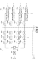
- Fig. 8G is a schematic diagram conceptually illustrating a part of the calculation of the addition unit 307.
- Fig. 8H is a schematic diagram conceptually illustrating a form of the data output by the addition unit 307.
- the output data of a large number of cross-spectrum calculation units 506 is combined into one set by the addition unit 307, and the form is the same as the form of the complex frequency data illustrated in Figs. 6C and 7E .
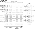
- Fig. 9I is a schematic diagram conceptually illustrating the calculation of the integration unit 308.
- the integration unit 308 performs integration processing on 512 sets of complex frequency data output from the addition unit 307, which are 16 ⁇ 10 6 pieces in the time axis direction, for each same frequency component. That is, the integration of the integration unit 308 is equivalent to time integration of the output data of the addition unit 307. Eventually, 512 sets of complex frequency data are obtained from the integration unit 308.
- the FFT 505 1024 pieces of data are input. If the FFT 505 is operated only once, data output from the A/D converter for 62.5 nsec is used. However, RFI is generated by various devices on the ground, and RFI caused by artificial radio waves is an extremely strong radio wave, compared with weak electromagnetic waves generated by natural objects. For this reason, in order to remove the influence of RFI as much as possible, it is preferable to sufficiently reduce the influence of RFI by time-integration for a long time. Thus, a measurement for a long time of one second is performed, the FFT 505 is repeatedly operated for the obtained enormous digital data, and the cross spectrum of each set of antennas is calculated. After all of the cross spectra are added, the integration unit 308 performs the time integration.
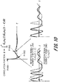
- Fig. 10 is a conceptual diagram illustrating an operation principle of the phased-array antenna device 101.
- ⁇ is a delay given to the antenna element 103.
- Fig. 10 illustrates that the cross correlation x is at the maximum value when ⁇ is 0 (point P1001), x decreases as soon as ⁇ starts to have a value (point P1002), x slightly increases as ⁇ further increases (point P1003), and thereafter, x converges to a value around 0 as ⁇ increases. Therefore, if ⁇ is electrically changed, it is possible to change the reception sensitivity azimuth of the cross correlation obtained from the two antenna elements 103.
- the inventors performed almost the same signal processing and data processing as shown in Figs. 3 and 5 , using two antenna elements 103 to receive microwaves of a plurality of frequencies.
- Fig. 11A is a graph schematically illustrating a result of receiving a microwave of a single frequency using two antenna elements 103 and performing cross-spectrum calculation processing.
- the horizontal axis represents the azimuth, and the vertical axis represents the normalized cross spectrum intensity.
- Fig. 11B is a graph schematically illustrating a result of receiving a microwave of three different frequencies using two antenna elements 103 and performing cross-spectrum calculation processing.
- the horizontal axis represents the azimuth, and the vertical axis represents the normalized cross spectrum intensity. Therefore, there is no unit on the vertical axis.
- Fig. 11A illustrates that the cross spectrum is the maximum value at an azimuth of 0° and that the cross spectrum periodically increases or decreases as the azimuth deviates.
- the area where the gain increases or decreases deviating from the center of the original azimuth is a grating lobe.
- Fig. 11B shows that the cross spectrum is the maximum value at the azimuth of 0° even in the case of a plurality of frequencies, and that the grating lobe increases or decreases depending on the frequencies.
- the phased-array antenna device 101 described above has a shape in which the antenna array is developed in the longitudinal and lateral directions as illustrated in Fig. 1 in order to form a point-like antenna beam having sharp directivity in a three-dimensional space, but may be a straight antenna array if the directivity of the antenna in a two-dimensional space is considered.
- the phased-array antenna device 101 described above has the following configuration.
- the first-row first-column antenna element 103a is used as a reference and is described as a first antenna element. Then, the first-row first-column preamplifier 303a that amplifies the signal output from the first-row first-column antenna element 103a can be described as a first preamplifier that amplifies the signal obtained from the first antenna element.
- the first-row first-column BPF group 304a that passes only a signal in a predetermined frequency band from the output signal of the first-row first-column preamplifier 303a can be described as a first BPF that passes only a signal in a predetermined frequency band from the output signal of the first preamplifier.
- the first-row first-column A/D converter group 305a that converts the output signal of the first-row first-column BPF group 304a into digital data can be described as a first A/D converter that converts the output signal of the first BPF into digital data.
- the first-row first-column FFT group 301a that performs a Fourier transform on the data output from the first-row first-column A/D converter group 305a can be described as a first FFT that performs a Fourier transform on the data output from the first A/D converter.
- the first-row second-column antenna element 103b arranged next to the first-row first-column antenna element 103a, spaced apart by the distance d can be described as a second antenna element arranged apart from the first antenna element by a predetermined distance.
- the first-row second-column preamplifier 303b that amplifies the signal output from the first-row second-column antenna element 103b can be described as a second preamplifier that amplifies the signal obtained from the second antenna element.
- the first-row second-column BPF group 304b that passes only a signal in a predetermined frequency band from the output signal of the first-row second-column preamplifier 303b can be described as a second BPF that passes only a signal in a predetermined frequency band from the output signal of the second preamplifier.
- the first-row second-column A/D converter group 305b that converts the output signal of the first-row second-column BPF group 304b into digital data can be described as a second A/D converter that converts the output signal of the second BPF into digital data.
- the first-row second-column FFT group 301b that performs a Fourier transform on the data output from the first-row second-column A/D converter group 305b can be described as a second FFT that performs a Fourier transform on the data output from the second A/D converter.
- the first cross-spectrum calculation unit group 302a that multiplies the output data of the first-row first-column FFT group 301a and the output data of the first-row second-column FFT group 301b for the same complex frequency component after converting one of them into a conjugate complex number can be described as a first cross-spectrum calculation unit that multiplies the output data of the first FFT and the output data of the second FFT for the same complex frequency component after converting one of them into a conjugate complex number.
- the clock control unit 106 that supplies a sampling clock whose output timing is relatively shifted to the first-row first-column A/D converter group 305a and the first-row second-column A/D converter group 305b can be described as a clock control unit that supplies a sampling clock whose output timing is relatively shifted to the first A/D converter and the second A/D converter.
- the first-row third-column antenna element 103c is arranged on a straight line on which the first-row first-column antenna element 103a and the first-row second-column antenna element 103b are arranged, spaced apart from the first-row second-column antenna element 103b by a distance that is a natural number multiple of the distance between the first-row first-column antenna element 103a and the first-row second-column antenna element 103b.
- the first-row third-column antenna element 103c can be described as a third antenna element that is arranged on a straight line on which the first antenna element and the second antenna element are arranged, spaced apart from the second antenna element by a distance that is a natural number multiple of the distance between the first antenna element and the second antenna element.
- the first-row third-column preamplifier 303c that amplifies the signal obtained from the first-row third-column antenna element 103c can be described as a third preamplifier that amplifies the signal obtained from the third antenna element.
- the first-row third-column BPF group 304c that passes only a signal in the same frequency band as the first-row first-column BPF group 304a from the output signal of the first-row third-column preamplifier 303c can be described as a third BPF that passes only a signal in in the same frequency band as the first BPF from the output signal of the third preamplifier.
- the first-row third-column A/D converter group 305c that converts the output signal of the first-row third-column BPF group 304c into digital data can be described as a third A/D converter that converts the output signal of the third BPF into digital data.
- the first-row third-column FFT group 301c that performs a Fourier transform on the data output from the first-row third-column A/D converter group 305c can be described as a third FFT that performs a Fourier transform on the data output from the third A/D converter.
- the fourth cross-spectrum calculation unit group 302d that multiplies the output data of the first-row first-column FFT group 301a and the output data of the first-row third-column FFT group 301c for the same complex frequency component after converting one of them into a conjugate complex number can be described as a second cross-spectrum calculation unit that multiplies the output data of the first FFT and the output data of the third FFT for the same complex frequency component after converting one of them into a conjugate complex number.
- the third cross-spectrum calculation unit group 302c that multiplies the output data of the first-row second-column FFT group 301b and the output data of the first-row third-column FFT group 301c for the same complex frequency component after converting one of them into a conjugate complex number can be described as a third cross-spectrum calculation unit that multiplies the output data of the second FFT and the output data of the third FFT for the same complex frequency component after converting one of them into a conjugate complex number.
- the second-row first-column antenna element 103e is arranged on a straight line orthogonal to the straight line on which the first-row first-column antenna element 103a and the first-row second-column antenna element 103b are arranged and on a straight line intersecting the first-row first-column antenna element 103a, spaced apart from the first-row first-column antenna element 103a by a distance that is a natural number multiple of the distance between the first-row first-column antenna element 103a and the first-row second-column antenna element 103b.
- the second-row first-column antenna element 103e can be described as a fourth antenna element that is arranged on a straight line orthogonal to the straight line on which the first antenna element and the second antenna element are arranged and on a straight line intersecting the first antenna element, spaced apart from the first antenna element by a distance that is a natural number multiple of the distance between the first antenna element and the second antenna element.
- the second-row first-column antenna element 103e there is a preamplifier, which is not illustrated in Fig. 4 , that amplifies the signal obtained from the second-row first-column antenna element 103e, similarly to the first-row first-column antenna element 103a, the first-row second-column antenna element 103b, the first-row third-column antenna element 103c, and the first-row fourth-column antenna element 103d.
- This preamplifier can be described as a fourth preamplifier that amplifies the signal obtained from the fourth antenna element.
- a BPF group which is not illustrated in Fig. 4 , that passes only a signal in the same frequency band as the first-row first-column BPF group 304a from the output signal of the preamplifier.
- This BPF group can be described as a fourth BPF that passes only a signal in the same frequency band as the first BPF from the output signal of the fourth preamplifier.
- an A/D converter group which is not illustrated in Fig. 4 , that converts the output signal of the BPF group into digital data.
- This A/D converter group can be described as a fourth A/D converter that converts the output signal of the fourth BPF into digital data.
- an FFT for the A/D converter group that converts the signal obtained from the second-row first-column antenna element 103e into digital data, there is an FFT, which is not illustrated in Fig. 4 , that performs a Fourier transform on the output data of the A/D converter group.
- This FFT can be described as a fourth FFT that performs Fourier transform on the data output from the fourth A/D converter.
- the fifth cross-spectrum calculation groups 402a which is not illustrated in Fig. 4 , includes six cross-spectrum calculation unit groups 302 (not illustrated) that process signals of the first-row first-column antenna element 103a, the second-row first-column antenna element 103e, the third-row first-column antenna element 103i, and the fourth-row first-column antenna element 103m. Therefore, for the fifth cross-spectrum calculation group 402a, there is a cross-spectrum calculation unit group, which corresponds to the first cross-spectrum calculation unit group 302a in Fig. 4 , that processes signals of the first-row first-column antenna element 103a and the second-row first-column antenna element 103e.
- the cross-spectrum calculation unit group can be described as a fourth cross-spectrum calculation unit that multiplies the output data of the first FFT and the output data of the fourth FFT for the same complex frequency components after converting one of them into the a conjugate complex number.
- the combination of the arrangement of the antenna elements 103 and the cross-spectrum calculation unit group 302 using the technique disclosed in Non-Patent Literature 2 described with reference to Figs. 1 to 4 is a technique for achieving sharp directivity of the phased-array antenna device 101.
- the phased-array antenna device 101 achieves the arrangement of the antenna elements 103 corresponding to the technique in Non-Patent Literature 2 at the positions corresponding to the sides of the frame 102. Therefore, the number of the cross-spectrum calculation unit groups 302 of the above phased-array antenna device 101 is 48 as described above.
- phased-array antenna device 101 is not limited to the combination of the arrangement of the antenna elements 103 and the cross-spectrum calculation unit group 302 based on the technique disclosed in Non-Patent Literature 2.
- the combination of the antenna elements 103 may not be necessarily based on the technique disclosed in Non-Patent Literature 2.
- the number of cross-spectrum calculation unit groups 302 is not limited to 48, and 120 cross-spectrum calculation unit groups 302 can be arranged.
- phased-array antenna device 101 has been described.
- the phased-array antenna device 101 uses a combination of the antenna elements 103 from which redundancy is eliminated, and directly performs A/D conversion on analog signals over a broad frequency range immediately under the antenna elements 103. At that time, by relatively shifting the supply timing of the sampling clock supplied to the A/D converter according to a desired azimuth with respect to the output analog signals of the two antenna elements 103, a time difference is given to the output digital data obtained from the two antenna elements 103. The time difference is obtained by multiplying the number of steps to shift the sampling clock according to the distance between the two antenna elements 103 by a natural number.
- the data output from the A/D converter is converted into complex frequency component data by the FFT 505.
- the complex frequency component data output from the FFTs 505 of two systems is multiplied after the complex frequency component data output from one of the FFTs 505 is converted into a conjugate complex number by the cross-spectrum calculation unit.
- the complex frequency component data output from the cross-spectrum calculation unit is added for each of the same time and the same frequency component and then time-integrated to obtain the intensity data of the complex frequency component.
- the phased-array antenna device 101 according to the embodiment of the present invention employs a technical approach different from a conventional technique for handling radio waves. Normally, when high-frequency signals based on radio waves obtained from antennas are handled, tuning circuits and down-conversion to intermediate frequencies, and the like, are used. However, the phased-array antenna device 101 according to the embodiment of the present invention does not use a tuning circuit, a PLL, an intermediate frequency, or the like. The signal obtained from the antenna is directly A/D converted after passing through the BPF, and converted into data in a frequency domain by the FFT 505. In this series of analog signal processing, a tuning circuit or the like is not used.
- a signal having a frequency higher than a frequency that can be sampled by the A/D converter is detected using aliasing.
- the sampling frequency is set to an integral multiple of a hexadecimal number, a data sample suitable for the FFT 505 is provided.
- phased-array antenna device 101 As described above, it is possible for the phased-array antenna device 101 according to the embodiment of the present invention to detect weak electromagnetic waves over an extremely broad frequency range for each frequency component with a technical approach and various contrivances greatly different from conventional techniques for wireless communication and microwave radiometers. In addition, since the phased-array antenna device 101 according to the embodiment of the present invention does not use any mechanically movable component, it is obvious that the operating lifespan is longer than those of conventional products.
- phased-array antenna device 101 since the phased-array antenna device 101 does not need to rotationally be driven, it is possible to easily increase the scale of the device as compared with conventional products. This is advantageous in terms of spatial resolution of antenna devices.
Landscapes
- Physics & Mathematics (AREA)
- General Physics & Mathematics (AREA)
- Engineering & Computer Science (AREA)
- Electromagnetism (AREA)
- Computer Networks & Wireless Communication (AREA)
- Radar, Positioning & Navigation (AREA)
- Remote Sensing (AREA)
- Variable-Direction Aerials And Aerial Arrays (AREA)
- Radar Systems Or Details Thereof (AREA)
Applications Claiming Priority (2)
| Application Number | Priority Date | Filing Date | Title |
|---|---|---|---|
| JP2019224449A JP6721226B1 (ja) | 2019-12-12 | 2019-12-12 | フェーズドアレイアンテナ装置 |
| PCT/JP2020/022185 WO2021117269A1 (ja) | 2019-12-12 | 2020-06-04 | フェーズドアレイアンテナ装置 |
Publications (3)
| Publication Number | Publication Date |
|---|---|
| EP4075152A1 true EP4075152A1 (de) | 2022-10-19 |
| EP4075152A4 EP4075152A4 (de) | 2024-01-24 |
| EP4075152B1 EP4075152B1 (de) | 2025-06-25 |
Family
ID=71402443
Family Applications (1)
| Application Number | Title | Priority Date | Filing Date |
|---|---|---|---|
| EP20899133.1A Active EP4075152B1 (de) | 2019-12-12 | 2020-06-04 | Phasengesteuerte antennenvorrichtung |
Country Status (4)
| Country | Link |
|---|---|
| US (1) | US12160050B2 (de) |
| EP (1) | EP4075152B1 (de) |
| JP (1) | JP6721226B1 (de) |
| WO (1) | WO2021117269A1 (de) |
Families Citing this family (2)
| Publication number | Priority date | Publication date | Assignee | Title |
|---|---|---|---|---|
| JP7493193B1 (ja) | 2023-06-26 | 2024-05-31 | 国立研究開発法人宇宙航空研究開発機構 | フェーズドアレイアンテナ装置 |
| CN117276899B (zh) * | 2023-11-17 | 2024-02-23 | 中国科学院空天信息创新研究院 | 相控阵天线和无线电通信装置 |
Family Cites Families (9)
| Publication number | Priority date | Publication date | Assignee | Title |
|---|---|---|---|---|
| US4990925A (en) * | 1984-05-07 | 1991-02-05 | Hughes Aircraft Company | Interferometric radiometer |
| JPH0251074A (ja) | 1988-08-12 | 1990-02-21 | Natl Space Dev Agency Japan<Nasda> | 高空間分解能マイクロ波放射計 |
| JPH07209359A (ja) | 1994-01-10 | 1995-08-11 | Mitsubishi Electric Corp | 電子走査型マイクロ波放射計 |
| JP3642844B2 (ja) * | 1995-11-08 | 2005-04-27 | 株式会社アドバンテスト | 波源像可視化方法及び装置 |
| US5874916A (en) * | 1996-01-25 | 1999-02-23 | Lockheed Martin Corporation | Frequency selective TDOA/FDOA cross-correlation |
| JPH09211045A (ja) | 1996-02-02 | 1997-08-15 | Mitsubishi Electric Corp | 検波装置 |
| JP2007303855A (ja) * | 2006-05-09 | 2007-11-22 | System Box Japan株式会社 | 地球情報分析システム |
| DE102018202289A1 (de) * | 2018-02-15 | 2019-08-22 | Robert Bosch Gmbh | Winkelauflösender breitbandiger Radarsensor für Kraftfahrzeuge |
| CN110448810A (zh) | 2018-05-08 | 2019-11-15 | 河北亿邦医疗设备股份有限公司 | 一种微波辐射器阵列 |
-
2019
- 2019-12-12 JP JP2019224449A patent/JP6721226B1/ja active Active
-
2020
- 2020-06-04 US US17/784,246 patent/US12160050B2/en active Active
- 2020-06-04 EP EP20899133.1A patent/EP4075152B1/de active Active
- 2020-06-04 WO PCT/JP2020/022185 patent/WO2021117269A1/ja not_active Ceased
Also Published As
| Publication number | Publication date |
|---|---|
| JP6721226B1 (ja) | 2020-07-08 |
| EP4075152B1 (de) | 2025-06-25 |
| JP2021093679A (ja) | 2021-06-17 |
| US20230045598A1 (en) | 2023-02-09 |
| US12160050B2 (en) | 2024-12-03 |
| WO2021117269A1 (ja) | 2021-06-17 |
| EP4075152A4 (de) | 2024-01-24 |
Similar Documents
| Publication | Publication Date | Title |
|---|---|---|
| US9070972B2 (en) | Wideband beam forming device; wideband beam steering device and corresponding methods | |
| CN111273267B (zh) | 基于相控阵非相干散射雷达的信号处理方法、系统、装置 | |
| CN113325417B (zh) | 一种毫米波和太赫兹多频段雷达探测成像系统及方法 | |
| EP4075152B1 (de) | Phasengesteuerte antennenvorrichtung | |
| CN108828546B (zh) | 一种天基多通道动目标雷达接收处理系统及方法 | |
| Singer et al. | A new narrow beam Doppler radar at 3 MHz for studies of the high-latitude middle atmosphere | |
| Burnett et al. | Design and development of a wide-field fully cryogenic phased array feed for Arecibo | |
| Chippendale et al. | Measured aperture-array noise temperature of the Mark II phased array feed for ASKAP | |
| Yan et al. | The digital beam forming technique in AgileDARN high-frequency radar | |
| Fromenteze et al. | A precorrection method for passive UWB time-reversal beamformer | |
| Benthem et al. | EMBRACE: Results from an aperture array for radio astronomy | |
| Veidt et al. | The DRAO phased array feed demonstrator: Recent results | |
| RU2732803C1 (ru) | Способ цифрового формирования диаграммы направленности активной фазированной антенной решётки при излучении и приеме линейно-частотно-модулированных сигналов | |
| Rincon et al. | Development of NASA'S Next Generation L-Band Digital Beamforming Synthetic Aperture Radar (DBSAR-2) | |
| Stanislavsky et al. | Low‐frequency heliographic observations of the quiet Sun corona | |
| JP6415392B2 (ja) | 信号処理装置 | |
| Liu et al. | IMI (Interferometric microwave imager): AL/S/C tri-frequency radiometer for water cycle observation mission (WCOM) | |
| Alistarh et al. | Spectral smoothing by multiple radar pattern multiplication for improved accuracy | |
| McKay et al. | All-sky interferometric riometry | |
| Imbriale et al. | The design and performance of a wideband radio telescope for the GAVRT program | |
| Xue et al. | Development of the disk antenna array aperture synthesis millimeter wave radiometer | |
| Liu et al. | Phased Array Feed Experiments and Galactic H i Observations | |
| Cassanelli | Fast Radio Burst Localization with Very Long Baseline Interferometry | |
| Wu et al. | Phased Array Feed Experiments and Galactic HI Observations | |
| Christensen et al. | The geostationary atmospheric sounder (GAS) |
Legal Events
| Date | Code | Title | Description |
|---|---|---|---|
| STAA | Information on the status of an ep patent application or granted ep patent |
Free format text: STATUS: THE INTERNATIONAL PUBLICATION HAS BEEN MADE |
|
| PUAI | Public reference made under article 153(3) epc to a published international application that has entered the european phase |
Free format text: ORIGINAL CODE: 0009012 |
|
| STAA | Information on the status of an ep patent application or granted ep patent |
Free format text: STATUS: REQUEST FOR EXAMINATION WAS MADE |
|
| 17P | Request for examination filed |
Effective date: 20220712 |
|
| AK | Designated contracting states |
Kind code of ref document: A1 Designated state(s): AL AT BE BG CH CY CZ DE DK EE ES FI FR GB GR HR HU IE IS IT LI LT LU LV MC MK MT NL NO PL PT RO RS SE SI SK SM TR |
|
| DAV | Request for validation of the european patent (deleted) | ||
| DAX | Request for extension of the european patent (deleted) | ||
| RIC1 | Information provided on ipc code assigned before grant |
Ipc: G01S 7/02 20060101ALI20231212BHEP Ipc: H01Q 3/26 20060101ALI20231212BHEP Ipc: G01R 29/08 20060101AFI20231212BHEP |
|
| A4 | Supplementary search report drawn up and despatched |
Effective date: 20231222 |
|
| RIC1 | Information provided on ipc code assigned before grant |
Ipc: G01S 7/02 20060101ALI20231218BHEP Ipc: H01Q 3/26 20060101ALI20231218BHEP Ipc: G01R 29/08 20060101AFI20231218BHEP |
|
| GRAP | Despatch of communication of intention to grant a patent |
Free format text: ORIGINAL CODE: EPIDOSNIGR1 |
|
| STAA | Information on the status of an ep patent application or granted ep patent |
Free format text: STATUS: GRANT OF PATENT IS INTENDED |
|
| INTG | Intention to grant announced |
Effective date: 20241210 |
|
| GRAJ | Information related to disapproval of communication of intention to grant by the applicant or resumption of examination proceedings by the epo deleted |
Free format text: ORIGINAL CODE: EPIDOSDIGR1 |
|
| STAA | Information on the status of an ep patent application or granted ep patent |
Free format text: STATUS: REQUEST FOR EXAMINATION WAS MADE |
|
| GRAJ | Information related to disapproval of communication of intention to grant by the applicant or resumption of examination proceedings by the epo deleted |
Free format text: ORIGINAL CODE: EPIDOSDIGR1 |
|
| GRAP | Despatch of communication of intention to grant a patent |
Free format text: ORIGINAL CODE: EPIDOSNIGR1 |
|
| INTC | Intention to grant announced (deleted) | ||
| GRAP | Despatch of communication of intention to grant a patent |
Free format text: ORIGINAL CODE: EPIDOSNIGR1 |
|
| STAA | Information on the status of an ep patent application or granted ep patent |
Free format text: STATUS: GRANT OF PATENT IS INTENDED |
|
| GRAS | Grant fee paid |
Free format text: ORIGINAL CODE: EPIDOSNIGR3 |
|
| GRAA | (expected) grant |
Free format text: ORIGINAL CODE: 0009210 |
|
| STAA | Information on the status of an ep patent application or granted ep patent |
Free format text: STATUS: THE PATENT HAS BEEN GRANTED |
|
| INTG | Intention to grant announced |
Effective date: 20250502 |
|
| AK | Designated contracting states |
Kind code of ref document: B1 Designated state(s): AL AT BE BG CH CY CZ DE DK EE ES FI FR GB GR HR HU IE IS IT LI LT LU LV MC MK MT NL NO PL PT RO RS SE SI SK SM TR |
|
| REG | Reference to a national code |
Ref country code: GB Ref legal event code: FG4D |
|
| REG | Reference to a national code |
Ref country code: CH Ref legal event code: EP |
|
| REG | Reference to a national code |
Ref country code: CH Ref legal event code: EP |
|
| REG | Reference to a national code |
Ref country code: IE Ref legal event code: FG4D |
|
| REG | Reference to a national code |
Ref country code: DE Ref legal event code: R096 Ref document number: 602020053538 Country of ref document: DE |
|
| REG | Reference to a national code |
Ref country code: NL Ref legal event code: FP |
|
| PG25 | Lapsed in a contracting state [announced via postgrant information from national office to epo] |
Ref country code: FI Free format text: LAPSE BECAUSE OF FAILURE TO SUBMIT A TRANSLATION OF THE DESCRIPTION OR TO PAY THE FEE WITHIN THE PRESCRIBED TIME-LIMIT Effective date: 20250625 |
|
| REG | Reference to a national code |
Ref country code: LT Ref legal event code: MG9D |
|
| PG25 | Lapsed in a contracting state [announced via postgrant information from national office to epo] |
Ref country code: NO Free format text: LAPSE BECAUSE OF FAILURE TO SUBMIT A TRANSLATION OF THE DESCRIPTION OR TO PAY THE FEE WITHIN THE PRESCRIBED TIME-LIMIT Effective date: 20250925 Ref country code: GR Free format text: LAPSE BECAUSE OF FAILURE TO SUBMIT A TRANSLATION OF THE DESCRIPTION OR TO PAY THE FEE WITHIN THE PRESCRIBED TIME-LIMIT Effective date: 20250926 |
|
| PG25 | Lapsed in a contracting state [announced via postgrant information from national office to epo] |
Ref country code: BG Free format text: LAPSE BECAUSE OF FAILURE TO SUBMIT A TRANSLATION OF THE DESCRIPTION OR TO PAY THE FEE WITHIN THE PRESCRIBED TIME-LIMIT Effective date: 20250625 |
|
| PG25 | Lapsed in a contracting state [announced via postgrant information from national office to epo] |
Ref country code: HR Free format text: LAPSE BECAUSE OF FAILURE TO SUBMIT A TRANSLATION OF THE DESCRIPTION OR TO PAY THE FEE WITHIN THE PRESCRIBED TIME-LIMIT Effective date: 20250625 |
|
| PG25 | Lapsed in a contracting state [announced via postgrant information from national office to epo] |
Ref country code: RS Free format text: LAPSE BECAUSE OF FAILURE TO SUBMIT A TRANSLATION OF THE DESCRIPTION OR TO PAY THE FEE WITHIN THE PRESCRIBED TIME-LIMIT Effective date: 20250925 |
|
| PG25 | Lapsed in a contracting state [announced via postgrant information from national office to epo] |
Ref country code: LV Free format text: LAPSE BECAUSE OF FAILURE TO SUBMIT A TRANSLATION OF THE DESCRIPTION OR TO PAY THE FEE WITHIN THE PRESCRIBED TIME-LIMIT Effective date: 20250625 |
|
| PG25 | Lapsed in a contracting state [announced via postgrant information from national office to epo] |
Ref country code: PT Free format text: LAPSE BECAUSE OF FAILURE TO SUBMIT A TRANSLATION OF THE DESCRIPTION OR TO PAY THE FEE WITHIN THE PRESCRIBED TIME-LIMIT Effective date: 20251027 |
|
| REG | Reference to a national code |
Ref country code: AT Ref legal event code: MK05 Ref document number: 1806973 Country of ref document: AT Kind code of ref document: T Effective date: 20250625 |
|
| PG25 | Lapsed in a contracting state [announced via postgrant information from national office to epo] |
Ref country code: IS Free format text: LAPSE BECAUSE OF FAILURE TO SUBMIT A TRANSLATION OF THE DESCRIPTION OR TO PAY THE FEE WITHIN THE PRESCRIBED TIME-LIMIT Effective date: 20251025 |
|
| PG25 | Lapsed in a contracting state [announced via postgrant information from national office to epo] |
Ref country code: AT Free format text: LAPSE BECAUSE OF FAILURE TO SUBMIT A TRANSLATION OF THE DESCRIPTION OR TO PAY THE FEE WITHIN THE PRESCRIBED TIME-LIMIT Effective date: 20250625 Ref country code: SM Free format text: LAPSE BECAUSE OF FAILURE TO SUBMIT A TRANSLATION OF THE DESCRIPTION OR TO PAY THE FEE WITHIN THE PRESCRIBED TIME-LIMIT Effective date: 20250625 |
|
| PG25 | Lapsed in a contracting state [announced via postgrant information from national office to epo] |
Ref country code: CZ Free format text: LAPSE BECAUSE OF FAILURE TO SUBMIT A TRANSLATION OF THE DESCRIPTION OR TO PAY THE FEE WITHIN THE PRESCRIBED TIME-LIMIT Effective date: 20250625 |
|
| PG25 | Lapsed in a contracting state [announced via postgrant information from national office to epo] |
Ref country code: PL Free format text: LAPSE BECAUSE OF FAILURE TO SUBMIT A TRANSLATION OF THE DESCRIPTION OR TO PAY THE FEE WITHIN THE PRESCRIBED TIME-LIMIT Effective date: 20250625 |
|
| PG25 | Lapsed in a contracting state [announced via postgrant information from national office to epo] |
Ref country code: EE Free format text: LAPSE BECAUSE OF FAILURE TO SUBMIT A TRANSLATION OF THE DESCRIPTION OR TO PAY THE FEE WITHIN THE PRESCRIBED TIME-LIMIT Effective date: 20250625 |
|
| PG25 | Lapsed in a contracting state [announced via postgrant information from national office to epo] |
Ref country code: SK Free format text: LAPSE BECAUSE OF FAILURE TO SUBMIT A TRANSLATION OF THE DESCRIPTION OR TO PAY THE FEE WITHIN THE PRESCRIBED TIME-LIMIT Effective date: 20250625 |
|
| PG25 | Lapsed in a contracting state [announced via postgrant information from national office to epo] |
Ref country code: ES Free format text: LAPSE BECAUSE OF FAILURE TO SUBMIT A TRANSLATION OF THE DESCRIPTION OR TO PAY THE FEE WITHIN THE PRESCRIBED TIME-LIMIT Effective date: 20250625 |
|
| PG25 | Lapsed in a contracting state [announced via postgrant information from national office to epo] |
Ref country code: DK Free format text: LAPSE BECAUSE OF FAILURE TO SUBMIT A TRANSLATION OF THE DESCRIPTION OR TO PAY THE FEE WITHIN THE PRESCRIBED TIME-LIMIT Effective date: 20250625 |
|
| PG25 | Lapsed in a contracting state [announced via postgrant information from national office to epo] |
Ref country code: IT Free format text: LAPSE BECAUSE OF FAILURE TO SUBMIT A TRANSLATION OF THE DESCRIPTION OR TO PAY THE FEE WITHIN THE PRESCRIBED TIME-LIMIT Effective date: 20250625 |
|
| PLBE | No opposition filed within time limit |
Free format text: ORIGINAL CODE: 0009261 |
|
| STAA | Information on the status of an ep patent application or granted ep patent |
Free format text: STATUS: NO OPPOSITION FILED WITHIN TIME LIMIT |