EP4071675A1 - Quantum computing using signal manipulation elements - Google Patents
Quantum computing using signal manipulation elements Download PDFInfo
- Publication number
- EP4071675A1 EP4071675A1 EP22167317.1A EP22167317A EP4071675A1 EP 4071675 A1 EP4071675 A1 EP 4071675A1 EP 22167317 A EP22167317 A EP 22167317A EP 4071675 A1 EP4071675 A1 EP 4071675A1
- Authority
- EP
- European Patent Office
- Prior art keywords
- signal
- atomic object
- action
- manipulation
- atomic
- Prior art date
- Legal status (The legal status is an assumption and is not a legal conclusion. Google has not performed a legal analysis and makes no representation as to the accuracy of the status listed.)
- Pending
Links
Images







Classifications
-
- G—PHYSICS
- G06—COMPUTING OR CALCULATING; COUNTING
- G06N—COMPUTING ARRANGEMENTS BASED ON SPECIFIC COMPUTATIONAL MODELS
- G06N10/00—Quantum computing, i.e. information processing based on quantum-mechanical phenomena
- G06N10/40—Physical realisations or architectures of quantum processors or components for manipulating qubits, e.g. qubit coupling or qubit control
-
- G—PHYSICS
- G06—COMPUTING OR CALCULATING; COUNTING
- G06N—COMPUTING ARRANGEMENTS BASED ON SPECIFIC COMPUTATIONAL MODELS
- G06N10/00—Quantum computing, i.e. information processing based on quantum-mechanical phenomena
-
- G—PHYSICS
- G02—OPTICS
- G02B—OPTICAL ELEMENTS, SYSTEMS OR APPARATUS
- G02B1/00—Optical elements characterised by the material of which they are made; Optical coatings for optical elements
- G02B1/002—Optical elements characterised by the material of which they are made; Optical coatings for optical elements made of materials engineered to provide properties not available in nature, e.g. metamaterials
-
- B—PERFORMING OPERATIONS; TRANSPORTING
- B82—NANOTECHNOLOGY
- B82Y—SPECIFIC USES OR APPLICATIONS OF NANOSTRUCTURES; MEASUREMENT OR ANALYSIS OF NANOSTRUCTURES; MANUFACTURE OR TREATMENT OF NANOSTRUCTURES
- B82Y10/00—Nanotechnology for information processing, storage or transmission, e.g. quantum computing or single electron logic
-
- B—PERFORMING OPERATIONS; TRANSPORTING
- B82—NANOTECHNOLOGY
- B82Y—SPECIFIC USES OR APPLICATIONS OF NANOSTRUCTURES; MEASUREMENT OR ANALYSIS OF NANOSTRUCTURES; MANUFACTURE OR TREATMENT OF NANOSTRUCTURES
- B82Y20/00—Nanooptics, e.g. quantum optics or photonic crystals
Definitions
- gates and other functions of the quantum computer are performed by applying laser beams to ions contained within the ion trap. Delivering these laser beams to a large scale quantum computer is a significant challenge due to the low ion height above the trap, the Rayleigh range of the laser beams, and the amount of laser power that needs to be delivered to an ion within the trap to perform the functions of the quantum computer.
- the atomic object confinement apparatus is a surface ion trap.
- the one or more signal manipulation elements comprise at least one collection array and one or more action arrays associated with the respective atomic object position.
- the action array is configured for use in performing a quantum computer function selected from a group consisting of photoionization of an atomic object, state preparation of the atomic object, reading a quantum state of the atomic object, cooling the atomic object or an atomic object crystal comprising the atomic object, shelving the atomic object, repumping the atomic object, performing a single qubit gate on the atomic object, and performing a multiple qubit gate on a set of atomic objects comprising the atomic object.
- a quantum computer function selected from a group consisting of photoionization of an atomic object, state preparation of the atomic object, reading a quantum state of the atomic object, cooling the atomic object or an atomic object crystal comprising the atomic object, shelving the atomic object, repumping the atomic object, performing a single qubit gate on the atomic object, and performing a multiple qubit gate on a set of atomic objects comprising the atomic object.
- system further comprises a controller configured to control operation of the plurality of electrodes and the at least one manipulation source.
- the one or more optical elements comprise at least one of a double-layer metasurface beam splitter; a photonic integrated circuit chip and one or more bulk optical components; or a photonic integrated circuit chip having integrated metasurfaces.
- the atomic object is an atom and/or ion.
- the atomic object may be qubit atomic object of an atomic object crystal comprising two or more atomic objects, with, in an example embodiment, the two or more atomic objects of the atomic object crystal comprising atomic objects of at least two different atomic numbers.
- the atomic object confinement apparatus is an ion trap (e.g., a surface ion trap, Paul trap, and/or the like).
- each signal manipulation element is formed and/or configured for use in performing one or more functions (photoionization, state preparation, qubit detection and/or reading, cooling, shelving, repumping, single qubit gates, or two qubit gates) of a QCCD-based quantum computer.
- a signal management element is a metamaterial array comprising a plurality of metamaterial structures.
- each of the plurality of metamaterial structures are positive metamaterial structures (e.g., pillars, columns, cylinders, and/or the like).
- each of the plurality of metamaterial structures are negative metamaterial structures (e.g., holes, pits, pockets, bubbles, and/or the like).
- a metamaterial array may comprise a combination of positive and negative metamaterial structures.
- some of the metamaterial arrays consist of and/or comprise positive metamaterial structures and other metamaterial arrays consist of and/or comprise negative metamaterial structures.
- the chromatic filtering performed by the signal manipulation element causes the controlled induced signal to only include a respective particular wavelength and/or wavelengths of the respective particular wavelength range the signal manipulation element is configured for use with. For example, an incoming manipulation signal incident on a signal manipulation element will only be focused onto the corresponding atomic object position when the incoming manipulation signal is characterized by a wavelength within the respective particular wavelength range.
- the detecting beam is emitted in a known direction such that the detecting beam may be captured (e.g., via collection optics and/or the like) and provided (e.g., via a fiber optics cable, waveguide, and/or the like) to a photodetector (e.g., photodiode, photomultiplier tube, charge-coupled device (CCD) sensor, complementary metal-oxide-semiconductor (CMOS) sensor, and/or other photodetector).
- a photodetector e.g., photodiode, photomultiplier tube, charge-coupled device (CCD) sensor, complementary metal-oxide-semiconductor (CMOS) sensor, and/or other photodetector.
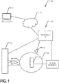
- Figure 1 provides a schematic diagram of an example quantum computing system 100 comprising an atomic object confinement apparatus 300 (e.g., an ion trap and/or the like), in accordance with an example embodiment.
- an atomic object confinement apparatus 300 e.g., an ion trap and/or the like
- a plurality of signal manipulation elements are formed and/or disposed on a surface of the atomic object confinement apparatus.
- at least a portion of the signal manipulation elements formed and/or disposed on the surface of the atomic object confinement apparatus are configured to be induced to emit an action signal toward and/or focused onto a respective atomic object position responsive to an incoming signal being incident thereon.
- the quantum computing system 100 comprises a computing entity 10 and a quantum computer 110.
- the quantum computer 110 comprises a controller 30, a cryostat and/or vacuum chamber 40 enclosing a confinement apparatus 300 (e.g., an ion trap), and one or more manipulation sources 60.
- the cryostat and/or vacuum chamber 40 may be a pressure-controlled chamber.
- the manipulation signals generated by the manipulation sources 60 are provided to the interior of the cryostat and/or vacuum chamber 40 (where the atomic object confinement apparatus 30 is located) via corresponding optical paths 66 (e.g., 66A, 66B, 66C).
- the optical paths 66 are defined, at least in part by one or more components and/or elements of the signal management system.
- at least one of the optical paths 66 comprises and/or is in part defined by a signal manipulation element of the signal management system.
- the manipulation sources 60 may be configured to generate one or more beams that may be used to initialize an atomic object into a state of a qubit space such that the atomic object may be used as a qubit of the confined atomic object quantum computer, perform one or more gates on one or more qubits of the confined atomic object quantum computer, read and/or determine a state of one or more qubits of the confined atomic object quantum computer, and/or the like.
- the quantum computer 110 comprises an optics collection system 70 configured to collect and/or detect photons generated by qubits (e.g., during reading procedures).
- the optics collection system 70 may comprise one or more optical elements (e.g., lenses, mirrors, waveguides, fiber optics cables, and/or the like) and one or more photodetectors.
- the photodetectors may be photodiodes, photomultipliers, charge-coupled device (CCD) sensors, complementary metal oxide semiconductor (CMOS) sensors, Micro-Electro-Mechanical Systems (MEMS) sensors, and/or other photodetectors that are sensitive to light at an expected fluorescence wavelength of the qubits of the quantum computer.
- the quantum computer 110 comprises one or more voltage sources 50.
- the voltage sources 50 may comprise a plurality of voltage drivers and/or voltage sources and/or at least one RF driver and/or voltage source.
- the voltage sources 50 may be electrically coupled to the corresponding potential generating elements (e.g., electrodes) of the confinement apparatus 300, in an example embodiment.
- the controller 30 is configured to control the voltage sources 50, cryostat system and/or vacuum system controlling the temperature and pressure within the cryostat and/or vacuum chamber 40, manipulation sources 60, optics collection system 70, and/or other systems controlling various environmental conditions (e.g., temperature, pressure, and/or the like) within the cryostat and/or vacuum chamber 40 and/or configured to manipulate and/or cause a controlled evolution of quantum states of one or more atomic objects within the confinement apparatus.
- the controller 30 may cause a controlled evolution of quantum states of one or more atomic objects within the confinement apparatus to execute a quantum circuit and/or algorithm.
- the controller 30 may cause a reading procedure comprising coherent shelving to be performed, possibly as part of executing a quantum circuit and/or algorithm.
- the atomic objects confined within the confinement apparatus are used as qubits of the quantum computer 110.
- the atomic object confinement apparatus comprises a plurality of electrodes that are configured to generate a confining potential.
- the controller 30 may control the voltage sources 50 to provide electrical signals to the electrodes of the atomic object confinement apparatus such that the electrodes generate a confining potential.
- the confining potential is configured to confine a plurality of atomic objects within a confinement volume defined by the atomic object confinement apparatus.
- the atomic object confinement apparatus is a surface ion trap and the confinement volume is a volume located proximate the surface of the surface ion trap.
- the electrodes and/or confining potential are configured to define a plurality of atomic object positions within the confinement volume.
- the atomic object positions are disposed in a one-dimensional or two-dimensional lay out.
- the atomic object positions are disposed along an axis of a linear atomic object confinement apparatus.
- the atomic object positions are disposed in a two-dimensional array or layout defined by a two-dimensional atomic object confinement apparatus.
- An example linear atomic object confinement apparatus is described by U.S. Application No. 16/717,602, filed December 17, 2019 , though various other linear atomic object confinement apparatuses may be used in various embodiments.
- An example two-dimensional atomic object confinement apparatus is described by EP 21215443.9, filed December 17, 2021 claiming priority of by U.S. Application No. 63/199,279, filed December 17, 2020 , though various other two-dimensional atomic object confinement apparatuses may be used in various embodiments.
- the confining potential evolves with time, based on the electrical signals provided to the electrodes by the voltage sources 50.
- the evolving of the confining potential may be configured to cause one or more atomic objects to move from respective first atomic object positions to respective second atomic object positions.
- Figures 2 and 3 each illustrate portions of an example two-dimensional atomic object confinement apparatus 300 comprising sequences of electrodes 310 that are separated by a spacing factor ⁇ .
- the spacing factor ⁇ is in a range between 500 ⁇ m and 1000 ⁇ m (e.g., approximately 750 ⁇ m).
- the sequences of electrodes 310 define a plurality of atomic object positions 305.
- an atomic object position 305 is a volume corresponding to a portion of an atomic object path 320 where the electrodes 310 are configured to maintain an atomic object (e.g., as part of an atomic object crystal) and/or a pair or set of atomic objects (e.g., for performing two or more qubit gates) for the performance of a function of the quantum computer and/or to store one or more atomic objects during the performance of functions of the quantum computer on other atomic objects located at other atomic positions.
- an atomic object e.g., as part of an atomic object crystal
- a pair or set of atomic objects e.g., for performing two or more qubit gates
- the sequences of electrodes 310 define a plurality of islands 330 and atomic object paths 320.
- the atomic objects may travel between various atomic object positions 305 along atomic object paths 320. In general, the atomic objects are not located over the islands 330.
- one or more signal manipulation elements e.g., action arrays
- one or more signal manipulation elements e.g., collection arrays
- the voltage sources 50 provide electrical signals to the potential generating elements (e.g., electrodes 310) of the confinement apparatus 300, such that a confining potential is formed. Based on the contours and time evolution of the confining potential one or more atomic objects are confined at respective atomic object positions, moved between atomic object positions and/or the like.
- one or more functions e.g., quantum computing functions
- An example function that may be performed on an atomic object is photoionization of the atomic object.
- a manipulation signal may be applied to the atomic object to photo ionize the atomic object.
- a manipulation signal e.g., a reading signal
- the atomic object's wave function collapses into a first state of the qubit space
- the atomic object will fluoresce in response to the reading signal being applied thereto.
- the atomic object's wave function collapses into a second state of the qubit space
- the atomic object will not fluoresce in response to the reading signal being applied thereto.
- An atomic object crystal is a pair or set of atomic objects where one of the atomic objects of the atomic object crystal is qubit atomic object used as a qubit of the quantum computer and the one or more other atomic objects of the atomic object crystal are used to perform sympathetic cooling of the qubit atomic object.
- a manipulation signal e.g., a cooling signal or a sympathetic cooling signal
- the shelving of an atomic object is performed by applying one or more manipulation signals to the atomic object to cause the atomic object's quantum state to evolve to an at least meta-stable state outside of the qubit space when the atomic object is in the second state of the qubit space.
- repumping of the atomic object comprises applying one or more manipulation signals to the atomic object to cause the quantum state of the atomic object to evolve to an excited state.
- Another example function that may be performed on an atomic object is performing a two qubit gate on the atomic object.
- one or more manipulation signals may be applied to a pair or set of atomic objects that includes the atomic object to perform a two qubit (or three, four, or more) quantum gate on the atomic object and the at least one other atomic object.
- the action signal is an appropriate signal (e.g., having an appropriate wavelength, polarization, amplitude, and/or the like) for causing the corresponding function to be performed responsive to the action signal (and possibly application of other action signals, magnetic fields, and/or the like) being incident on an atomic object (or set of atomic objects) at the corresponding atomic object position.
- an appropriate signal e.g., having an appropriate wavelength, polarization, amplitude, and/or the like
- a second substrate 910 is mounted and/or secured in relationship to the atomic object confinement apparatus 300 and signal manipulation elements (and/or arrangements of signal manipulation elements) are formed and/or disposed on a surface of the second substrate, as illustrated in Figure 9 .
- the metamaterial structures are Huygen's metamaterial structures.
- an electric dipole and a magnetic dipole are induced, causing each metamaterial structure to generate an electromagnetic wave like a Huygen's wavelet when an appropriate electromagnetic beam, signal, wave, and/or the like is incident on the metamaterial structure.
- the phases of the magnetic dipole and the electric dipole determine the phase, direction, and/or polarization of the electromagnetic wave, radiation, beam, and/or signal emitted by the metamaterial structure.
- one or more plasmonic photonic metasurfaces are used.
- the photonic metasurfaces are dielectric and/or plasmonic metasurfaces using two or more electric or magnetic resonances of any order to locally engineer the desired phase and amplitude response of the respective photonic metasurface.
- Various other types of metamaterial structures that define various types of metamaterial surfaces are used in various embodiments.
- At least one of the signal manipulation elements is a DOE or an assembly of DOEs.
- a DOE is an optical element having characteristics that have dimensions on a scale larger than the respective particular wavelength of light.
- a signal manipulation element may be a DOE configured to control the polarization of an induced signal (e.g., action signal and/or collection signal), focus and/or collimate the induced signal, chromatically filter the induced signal, control the phase of the induced signal, and/or the like, in an example embodiment.
- a signal manipulation element comprises both a metamaterial array (e.g., a plurality of metamaterial structures) and a DOE component.
- the signal manipulation element(s) are formed, deposited, and/or disposed on the surface of atomic object confinement apparatus.
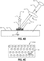
- Figure 4A illustrates a partial cross-sectional view of an atomic object confinement apparatus wherein action arrays 400 are used to apply manipulation signals to an atomic object position 305.
- the controller 30 controls one or more manipulation sources 60 to generate manipulation signals.
- the manipulation signals are provided to the atomic object confinement apparatus 300 as incoming signals 62 propagating transverse to a plane defined by a surface 350 of the atomic object confinement apparatus 300 such that the incoming signals 62 are incident on action arrays 400.
- the incoming signals 62 being incident on the action arrays 400 cause respective induced action signals 64 to be emitted toward the corresponding atomic object position 305.
- Figure 4B illustrates a partial cross-sectional view of an atomic object confinement apparatus wherein a collection array 440 is used to collect an emitted signal generated by an atomic object 5 at a respective atomic object position 305.
- a collection array 440 is used to collect an emitted signal generated by an atomic object 5 at a respective atomic object position 305.
- an atomic object 5 located at the atomic object position 305 may be caused to emit an emitted signal 72.
- At least a portion of the emitted signal 72 is incident on the collection array 440.
- the at least a portion of the emitted signal 72 being incident on the collection array 440 causes an induced collection signal 74 to be emitted from the collection array 440 and toward a collection position 445.
- collection optics are located and/or disposed at the collection position 445.
- the collection optics comprise one or more optical elements, such as collection lens 420 configured to couple at least a portion of the collection signal 74 into a collection fiber 425.
- a signal manipulation element formed on and/or disposed on the surface 350 of the atomic object confinement apparatus 300 has a diameter that is in a range of 5 ⁇ m to 200 ⁇ m (e.g., approximately 100 ⁇ m).
- the signal manipulation element is at least three times the particular wavelength that the signal manipulation element is configured for use with in diameter.
- an incoming signal is a beam focused to a diameter of approximately 32 ⁇ m.
- the incoming signal may have a diameter of approximately 32 ⁇ m when the incoming signal interacts with the signal manipulation element.
- the signal manipulation element may have a diameter that is larger (e.g., a factor of one to seven times larger) than the diameter of an incoming signal beam.
- a first two qubit gate array 510A is configured to have incident thereon an incoming signal of a first wavelength and to emit an induced action signal corresponding to the first wavelength (e.g., substantially equal to the first wavelength, in an example embodiment) and a second two qubit gate array 510B is configured to have incident thereon an incoming signal of a second wavelength and to emit an induced action signal corresponding to the second wavelength (e.g., substantially equal to the second wavelength, in an example embodiment).
- the first and second wavelengths are not equal to one another.
- the first and second wavelengths are substantially equal to one another.
- the first and second wavelengths correspond to frequencies that are separated from one another by less than 15 GHz (e.g., approximately 12.64 GHz).
- a first cooling array 520A is configured to have incident thereon an incoming signal of a third wavelength and to emit an induced action signal corresponding to the third wavelength (e.g., substantially equal to the third wavelength, in an example embodiment) and a second cooling array 520B is configured to have incident thereon an incoming signal of a fourth wavelength and to emit an induced action signal corresponding to the fourth wavelength (e.g., substantially equal to the fourth wavelength, in an example embodiment).
- the third and fourth wavelengths are not equal to one another.
- the third wavelength is 493 nm and the fourth wavelength is 650 nm.
- the signal manipulation elements are configured to cause an action signal to be focused on the (entire) respective atomic object position and/or on one or more portions of the respective atomic object position.
- Figures 10A, 10B , and 10C illustrate a group of four atomic objects 5A, 5B, 5C, and 5D located at atomic object position 305.
- the group of atomic objects may be a four ion crystal, in an example embodiment.
- Figures 10A, 10B , and 10C each illustrate an example focus of an action signal by a respective signal manipulation element.
- various signal manipulation elements may be configured to provide respective action arrays focused in one or more of the illustrated manners or in other manners.
- the incoming lenses 1110 and/or collection lenses 420 are DOEs and/or transmissive metamaterial arrays configured to act as lenses.
- the distribution and positioning optical element 1210 comprises one or more modulators, waveguides, beam splitters (e.g., comprising DOEs and/or metamaterial arrays), lenses (e.g., incoming lenses 1110 and/or collection lenses 420), double-layer metamaterial array beam splitter 1300, photonic integrated circuit (PIC) 1400, and/or the like.
- free-space optical elements such as one or more acoustic optic modulators (AOMs) and/or one or more electro-optic deflectors could enable time division multiplexing of manipulation signals, which would reduce laser power requirements.
- the operation of the modulators, PIC 1400, and/or the like is controlled by the controller 30.
- the splitting metamaterial array 1310 and/or the collimating metamaterial arrays 1320 are configured to control the polarization and/or phase of the respective collimated signals 94.
- a PIC 1400 is used to generate a plurality of manipulation signals (e.g., from a manipulation signal generated by a manipulation source 60) and to provide the plurality of manipulation signals to respective action arrays associated with respective atomic object positions 305 of an atomic object confinement apparatus 300.
- Figure 14A illustrates a face-on view of an example PIC 1400 that may be used to provide manipulation signals to respective action arrays.
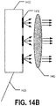
- Figure 14B illustrates a side view of the PIC 1400 where the PIC 1400 is used in coordination with bulk optical elements (e.g., lens 1440) to provide the manipulation signals to the respective action arrays.
- Figure 14C illustrates a side view of the PIC 1400 where metamaterial arrays 1450 are formed and/or disposed in the output windows 1410 of the PIC 1400 such that external optical components are not required for providing the manipulation signals to the respective action arrays.
- external and/or bulk optics such as lens 1440 to collimate and/or focus the signals exiting the optical windows 1410 of the PIC 1400 and direct the signals toward respective action arrays associated with respective atomic object positions 305 of the atomic object confinement apparatus 300.
- transmissive metamaterial arrays 1450 are disposed and/or formed in the optical windows 1410.
- the metamaterial arrays 1450 are configured to collimate and/or focus the signals exiting the optical windows 1410 of the PIC 1400 and direct the signals toward respective action arrays associated with respective atomic object positions 305 of the atomic object confinement apparatus 300.
- an alignment arrangement comprises one or more signal manipulation elements configured to detect the alignment or displacement from appropriate alignment with respect to rotation about an axis that is substantially parallel to the direction of propagation of the incoming signal, referred to herein as rotational alignment signal manipulation elements.
- rotational alignment signal manipulation elements For a linearly polarized incoming signal, rotation of the source is the same as rotation of the polarization of the incoming signal.
- the rotational alignment signal manipulation element is configured so that a positive rotation would approach resonance and a negative rotation would move further from resonance (or vice versa). As the derivative of the resonant response is maximized on the side of the resonant peak, such a rotational alignment signal manipulation element provides a highly sensitive measurement of the rotational alignment of the incoming signal optical path with respect to the rotational alignment signal manipulation element.
- the rotation alignment signal manipulation element uses an electric or magnetic dipole resonance.
- an alignment arrangement comprises two rotational alignment signal manipulation elements.
- a first rotational alignment signal manipulation element may be tuned so that nominal alignment corresponds to the center of the response peak and a second rotational alignment signal manipulation element may be tuned to maximize sensitivity and provide information about the rotation direction.
- nominal alignment for the second rotational alignment signal manipulation element may be approximately half way up the response peak.
- the first rotational alignment signal manipulation element may be used for an initial alignment and the second rotation alignment signal manipulation element may be used for fine-tuning the alignment, performing real-time adjustments to the alignment, and/or the like.
- an alignment arrangement comprises one or more signal manipulation elements configured to detect the alignment or displacement from appropriate alignment with respect to tilt along two independent directions that are substantially parallel to the plane defined by the surface 350 of the atomic object confinement apparatus 300, referred to herein as tilt alignment signal manipulation elements.
- a tilt alignment signal manipulation element is a uniform photonic metasurface (e.g., with no imposed gradient) with a sharp resonant peak (e.g., antisymmetric resonance, Fano resonance, BIC resonance, quasi-BIC resonance, and/or the like) that is highly sensitive to the angle of incidence of the incoming signal such that the forward-propagating amplitude is modulated based on the angle of incidence of the incoming signal.
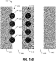
- An optical vortex has a zero-amplitude singularity at its center (e.g., the amplitude of the signal forms an annular structure, as illustrated in Figure 15A ).
- a first scatterer 1510A is, when appropriate parallel translational alignment is achieved, aligned with the zero-amplitude singularity at the center of the optical vortex.
- a second scatterer 1510B is, when appropriate parallel translational alignment is achieved, partially illuminated on the outward edge of the incoming signal 1520 ring, displaced in a first-direction from the first scatterer 1510A.
- a third scatterer 1510C is, when appropriate parallel translational alignment is achieved, partially illuminated on the outward edge of the incoming signal 1520 ring, displaced in a second-direction from the first scatterer 1510A.
- a second set of rows of scatterers and a second incoming signal in the form of a interference pattern comprising dark and bright fringes would be used for determining the displacement in a second (independent) direction that is also substantially parallel to the plane defined by the surface 350 of the atomic object confinement apparatus 300.
- use of a lateral displacement element 1500, 1550 comprises spatial filtering of the detected signal (e.g., the reflect/scattered signal due to the incident beam being incident on the lateral displacement element).
- the spatial filtering is performed by imaging the scatterers on the focal plane of a camera.
- Various other techniques for spatial filtering of a detected optical signal may be used in various other embodiments.
- a diffraction grating surrounding the multi-degree alignment metamaterial array would provide characteristic fringes if illuminated (e.g., by the incoming signal being not properly aligned with the multi-degree alignment metamaterial array).
- the multi-degree alignment metamaterial array may be configured with separate optical function for orthogonal linear polarizations to measure rotational misalignment. For instance, first-direction linearly-polarized light would be focused and deflected at an angle of theta, while second-direction linearly-polarized light would be focused and deflected at an angle of negative theta. Comparing the amplitudes of the two focal points would indicate the fractional intensity of both incident polarizations such that the rotational alignment or misalignment may be determined.
- a multi-degree alignment metamaterial array is used for initial alignment of the optical paths of the beam management system with corresponding action arrays associated with the atomic object confinement apparatus 300.
- One or more rotational alignment signal manipulation elements, tilt alignment signal manipulation elements, perpendicular translation alignment signal manipulation elements, and/or sets/rows of scattering elements are used to perform fine-alignment and/or real-time correction of alignment of optical paths of the beam management system with corresponding action arrays associated with the atomic object confinement apparatus 300.
- manipulation signals are sent transverse (e.g., approximately perpendicular) to a plane defined by the surface 350 of the atomic object confinement apparatus 300.
- the manipulation signals are sent such that they are incident on a signal manipulation element and induce the metamaterial structures of the array to emit an action signal that is focused on the corresponding atomic object positions.
- emitted signals emitted by an atomic object located at an atomic object position are incident on a signal manipulation element formed and/or disposed on the surface 350 and an induced collection signal is emitted out of the plane defined by the surface 350 toward a respective collection position.
- the signal manipulation elements are formed and/or disposed on the surface 350 of the atomic object confinement apparatus 300, motion of the atomic object confinement apparatus 300 will not lead to a beam point error. Rather, movement of the atomic object confinement apparatus may result in a minor amplitude error that can be compensated for through a calibration of the manipulation signal power.
- the metasurfaces of various embodiments make it possible to focus a single manipulation signal into two spots, each having a spot size of a few microns, that are separated by the required distance (e.g., approximately 8 microns). This enables a significant reduction in the required power of the manipulation signal. For example, in various embodiments, the required power of the manipulation signal is reduced by more than a factor of ten.
- Various embodiments further provide efficient techniques for defining optical paths and/or providing incoming signals to the action arrays and aligning the optical paths with the respective action arrays.
- various embodiments provide technical improvements to the technical field of providing manipulation signals to and collecting indications of emitted signals from atomic objects confined by an atomic object confinement apparatus.
- an atomic object confinement apparatus confinement apparatus 300 is incorporated into a system (e.g., a quantum computer 110) comprising a controller 30.
- the controller 30 is configured to control various elements of the system (e.g., quantum computer 110).
- the controller 30 may comprise various controller elements including processing elements 1605, memory 1610, driver controller elements 1615, a communication interface 1620, analog-digital converter elements 1625, and/or the like.
- the processing elements 1605 may comprise programmable logic devices (CPLDs), microprocessors, coprocessing entities, application-specific instruction-set processors (ASIPs), integrated circuits, application specific integrated circuits (ASICs), field programmable gate arrays (FPGAs), programmable logic arrays (PLAs), hardware accelerators, other processing devices and/or circuitry, and/or the like. and/or controllers.
- the term circuitry may refer to an entirely hardware embodiment or a combination of hardware and computer program products.
- the processing element 1605 of the controller 30 comprises a clock and/or is in communication with a clock.
- the memory 1610 may comprise non-transitory memory such as volatile and/or non-volatile memory storage such as one or more of as hard disks, ROM, PROM, EPROM, EEPROM, flash memory, MMCs, SD memory cards, Memory Sticks, CBRAM, PRAM, FeRAM, RRAM, SONOS, racetrack memory, RAM, DRAM, SRAM, FPM DRAM, EDO DRAM, SDRAM, DDR SDRAM, DDR2 SDRAM, DDR3 SDRAM, RDRAM, RIMM, DIMM, SIMM, VRAM, cache memory, register memory, and/or the like.
- volatile and/or non-volatile memory storage such as one or more of as hard disks, ROM, PROM, EPROM, EEPROM, flash memory, MMCs, SD memory cards, Memory Sticks, CBRAM, PRAM, FeRAM, RRAM, SONOS, racetrack memory, RAM, DRAM, SRAM, FPM DRAM, EDO DRAM, SDRAM, DDR SDRAM, DDR2
- the memory 1610 may store a queue of commands to be executed to cause a quantum algorithm and/or circuit to be executed (e.g., an executable queue), qubit records corresponding the qubits of quantum computer (e.g., in a qubit record data store, qubit record database, qubit record table, and/or the like), a calibration table, computer program code (e.g., in a one or more computer languages, specialized controller language(s), and/or the like), and/or the like.
- a queue of commands to be executed to cause a quantum algorithm and/or circuit to be executed e.g., an executable queue
- qubit records corresponding the qubits of quantum computer e.g., in a qubit record data store, qubit record database, qubit record table, and/or the like
- a calibration table e.g., computer program code (e.g., in a one or more computer languages, specialized controller language(s), and/or the like), and/or the like.
- execution of at least a portion of the computer program code stored in the memory 1610 causes the controller 30 to perform one or more steps, operations, processes, procedures and/or the like described herein for providing manipulation signals to atomic object positions and/or collecting, detecting, capturing, and/or measuring indications of emitted signals emitted by atomic objects located at corresponding atomic object positions of the atomic object confinement apparatus 300.
- the driver controller elements 1610 may include one or more drivers and/or controller elements each configured to control one or more drivers.
- the driver controller elements 1610 may comprise drivers and/or driver controllers.
- the driver controllers may be configured to cause one or more corresponding drivers to be operated in accordance with executable instructions, commands, and/or the like scheduled and executed by the controller 30 (e.g., by the processing element 1605).
- the driver controller elements 1615 may enable the controller 30 to operate a voltage sources 50, manipulation sources 60, cooling system, and/or the like.
- the drivers may be laser drivers configured to operate one or manipulation sources 60 to generate manipulation signals; vacuum component drivers; drivers for controlling the flow of current and/or voltage applied to electrodes used for maintaining and/or controlling the trapping potential of the atomic object confinement apparatus 300 (and/or other drivers for providing driver action sequences to potential generating elements of the atomic object confinement apparatus); cryostat and/or vacuum system component drivers; cooling system drivers, and/or the like.
- the controller 30 comprises means for communicating and/or receiving signals from one or more optical receiver components (e.g., photodetectors of the optics collection system).
- the controller 30 may comprise one or more analog-digital converter elements 1625 configured to receive signals from one or more optical receiver components (e.g., a photodetector of the optics collection system), calibration sensors, and/or the like.
- the controller 30 may comprise a communication interface 1620 for interfacing and/or communicating with a computing entity 10.
- the controller 30 may comprise a communication interface 1620 for receiving executable instructions, command sets, and/or the like from the computing entity 10 and providing output received from the quantum computer 110 (e.g., from an optical collection system) and/or the result of a processing the output to the computing entity 10.
- the computing entity 10 and the controller 30 may communicate via a direct wired and/or wireless connection and/or via one or more wired and/or wireless networks 20.
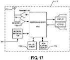
- Figure 17 provides an illustrative schematic representative of an example computing entity 10 that can be used in conjunction with embodiments of the present invention.
- a computing entity 10 is configured to allow a user to provide input to the quantum computer 110 (e.g., via a user interface of the computing entity 10) and receive, display, analyze, and/or the like output from the quantum computer 110.
- a computing entity 10 can include an antenna 1712, a transmitter 1704 (e.g., radio), a receiver 1706 (e.g., radio), and a processing element 1708 that provides signals to and receives signals from the transmitter 1704 and receiver 1706, respectively.
- the signals provided to and received from the transmitter 1704 and the receiver 1706, respectively, may include signaling information/data in accordance with an air interface standard of applicable wireless systems to communicate with various entities, such as a controller 30, other computing entities 10, and/or the like.
- the computing entity 10 may be capable of operating with one or more air interface standards, communication protocols, modulation types, and access types.
- the computing entity 10 may be configured to receive and/or provide communications using a wired data transmission protocol, such as fiber distributed data interface (FDDI), digital subscriber line (DSL), Ethernet, asynchronous transfer mode (ATM), frame relay, data over cable service interface specification (DOCSIS), or any other wired transmission protocol.
- a wired data transmission protocol such as fiber distributed data interface (FDDI), digital subscriber line (DSL), Ethernet, asynchronous transfer mode (ATM), frame relay, data over cable service interface specification (DOCSIS), or any other wired transmission protocol.
- FDDI fiber distributed data interface
- DSL digital subscriber line
- Ethernet asynchronous transfer mode
- ATM asynchronous transfer mode
- frame relay frame relay
- DOCSIS data over cable service interface specification
- the computing entity 10 may be configured to communicate via wireless external communication networks using any of a variety of protocols, such as general packet radio service (GPRS), Universal Mobile Telecommunications System (UMTS), Code Division Multiple Access 2000 (CDMA2000), CDMA2000 1X (1xRTT), Wideband Code Division Multiple Access (WCDMA), Global System for Mobile Communications (GSM), Enhanced Data rates for GSM Evolution (EDGE), Time Division-Synchronous Code Division Multiple Access (TD-SCDMA), Long Term Evolution (LTE), Evolved Universal Terrestrial Radio Access Network (E-UTRAN), Evolution-Data Optimized (EVDO), High Speed Packet Access (HSPA), High-Speed Downlink Packet Access (HSDPA), IEEE 802.11 (Wi-Fi), Wi-Fi Direct, 802.16 (WiMAX), ultra wideband (UWB), infrared (IR) protocols, near field communication (NFC) protocols, Wibree, Bluetooth protocols, wireless universal serial bus (USB) protocols, and/or any other wireless protocol.
- GPRS general
- the computing entity 10 may use such protocols and standards to communicate using Border Gateway Protocol (BGP), Dynamic Host Configuration Protocol (DHCP), Domain Name System (DNS), File Transfer Protocol (FTP), Hypertext Transfer Protocol (HTTP), HTTP over TLS/SSL/Secure, Internet Message Access Protocol (IMAP), Network Time Protocol (NTP), Simple Mail Transfer Protocol (SMTP), Telnet, Transport Layer Security (TLS), Secure Sockets Layer (SSL), Internet Protocol (IP), Transmission Control Protocol (TCP), User Datagram Protocol (UDP), Datagram Congestion Control Protocol (DCCP), Stream Control Transmission Protocol (SCTP), HyperText Markup Language (HTML), and/or the like.
- Border Gateway Protocol BGP
- Dynamic Host Configuration Protocol DHCP
- DNS Domain Name System
- FTP File Transfer Protocol
- HTTP Hypertext Transfer Protocol
- HTTP Hypertext Transfer Protocol
- HTTP HyperText Transfer Protocol
- HTTP HyperText Markup Language
- IP Internet Protocol
- TCP Transmission Control Protocol
- UDP User Datagram Protocol
- DCCP
- the computing entity 10 can communicate with various other entities using concepts such as Unstructured Supplementary Service information/data (USSD), Short Message Service (SMS), Multimedia Messaging Service (MMS), Dual-Tone Multi-Frequency Signaling (DTMF), and/or Subscriber Identity Module Dialer (SIM dialer).
- USSD Unstructured Supplementary Service information/data
- SMS Short Message Service
- MMS Multimedia Messaging Service
- DTMF Dual-Tone Multi-Frequency Signaling
- SIM dialer Subscriber Identity Module Dialer
- the computing entity 10 can also download changes, add-ons, and updates, for instance, to its firmware, software (e.g., including executable instructions, applications, program modules), and operating system.
- the computing entity 10 may also comprise a user interface device comprising one or more user input/output interfaces (e.g., a display 1716 and/or speaker/speaker driver coupled to a processing element 1708 and a touch screen, keyboard, mouse, and/or microphone coupled to a processing element 1708).
- the user output interface may be configured to provide an application, browser, user interface, interface, dashboard, screen, webpage, page, and/or similar words used herein interchangeably executing on and/or accessible via the computing entity 10 to cause display or audible presentation of information/data and for interaction therewith via one or more user input interfaces.
- the user input interface can comprise any of a number of devices allowing the computing entity 10 to receive data, such as a keypad 1718 (hard or soft), a touch display, voice/speech or motion interfaces, scanners, readers, or other input device.
- a keypad 1718 can include (or cause display of) the conventional numeric (0-9) and related keys (#, ⁇ ), and other keys used for operating the computing entity 10 and may include a full set of alphabetic keys or set of keys that may be activated to provide a full set of alphanumeric keys.
- the user input interface can be used, for example, to activate or deactivate certain functions, such as screen savers and/or sleep modes. Through such inputs the computing entity 10 can collect information/data, user interaction/input, and/or the like.
- the computing entity 10 can also include volatile storage or memory 1722 and/or non-volatile storage or memory 1724, which can be embedded and/or may be removable.
- the non-volatile memory may be ROM, PROM, EPROM, EEPROM, flash memory, MMCs, SD memory cards, Memory Sticks, CBRAM, PRAM, FeRAM, RRAM, SONOS, racetrack memory, and/or the like.
- the volatile memory may be RAM, DRAM, SRAM, FPM DRAM, EDO DRAM, SDRAM, DDR SDRAM, DDR2 SDRAM, DDR3 SDRAM, RDRAM, RIMM, DIMM, SIMM, VRAM, cache memory, register memory, and/or the like.
- the volatile and non-volatile storage or memory can store databases, database instances, database management system entities, data, applications, programs, program modules, scripts, source code, object code, byte code, compiled code, interpreted code, machine code, executable instructions, and/or the like to implement the functions of the computing entity 10.
- the present subject-matter includes, inter alia, the following aspects:
Landscapes
- Physics & Mathematics (AREA)
- General Physics & Mathematics (AREA)
- Engineering & Computer Science (AREA)
- Theoretical Computer Science (AREA)
- Mathematical Optimization (AREA)
- Pure & Applied Mathematics (AREA)
- Condensed Matter Physics & Semiconductors (AREA)
- Data Mining & Analysis (AREA)
- Evolutionary Computation (AREA)
- Mathematical Analysis (AREA)
- Artificial Intelligence (AREA)
- Computational Mathematics (AREA)
- Computing Systems (AREA)
- General Engineering & Computer Science (AREA)
- Mathematical Physics (AREA)
- Software Systems (AREA)
- Optics & Photonics (AREA)
- Optical Modulation, Optical Deflection, Nonlinear Optics, Optical Demodulation, Optical Logic Elements (AREA)
- Physical Or Chemical Processes And Apparatus (AREA)
- Electron Tubes For Measurement (AREA)
Applications Claiming Priority (2)
| Application Number | Priority Date | Filing Date | Title |
|---|---|---|---|
| US202163201018P | 2021-04-08 | 2021-04-08 | |
| US17/653,979 US12217132B2 (en) | 2021-04-08 | 2022-03-08 | Quantum computing using metamaterial arrays |
Publications (1)
| Publication Number | Publication Date |
|---|---|
| EP4071675A1 true EP4071675A1 (en) | 2022-10-12 |
Family
ID=81306775
Family Applications (1)
| Application Number | Title | Priority Date | Filing Date |
|---|---|---|---|
| EP22167317.1A Pending EP4071675A1 (en) | 2021-04-08 | 2022-04-08 | Quantum computing using signal manipulation elements |
Country Status (5)
| Country | Link |
|---|---|
| US (1) | US12217132B2 (https=) |
| EP (1) | EP4071675A1 (https=) |
| JP (1) | JP2022161879A (https=) |
| CN (1) | CN115238897A (https=) |
| TW (1) | TW202247054A (https=) |
Cited By (2)
| Publication number | Priority date | Publication date | Assignee | Title |
|---|---|---|---|---|
| WO2024133910A1 (en) * | 2022-12-22 | 2024-06-27 | Universal Quantum Ltd | Improvements in or relating to quantum computing |
| WO2025230561A3 (en) * | 2023-09-08 | 2026-03-12 | Quantinuum Llc | Entanglement apparatus with reflectors on a quantum device |
Families Citing this family (8)
| Publication number | Priority date | Publication date | Assignee | Title |
|---|---|---|---|---|
| US12327651B2 (en) * | 2021-08-19 | 2025-06-10 | Quantinuum Llc | Periodic multi-dimensional atomic object confinement apparatus having curved legs |
| US12411263B2 (en) * | 2021-09-08 | 2025-09-09 | ColdQuanta, Inc. | Ultra-high-vacuum cell with integrated meta-optics |
| CN115901670B (zh) * | 2022-11-09 | 2025-07-25 | 山东科技大学 | 一种由多个连续域束缚态支配的可调谐太赫兹传感器 |
| EP4732203A1 (en) * | 2023-06-20 | 2026-04-29 | Quantinuum LLC | Confinement apparatus system with integrated ferromagnetic structures |
| US20250014772A1 (en) * | 2023-07-05 | 2025-01-09 | Quantinuum Llc | Optics-integrated confinement apparatus including polarization controlling optical elements |
| WO2025038349A1 (en) * | 2023-08-14 | 2025-02-20 | Quantinuum Llc | Signal manipulation elements integrated with window plate for optical feedthrough to vacuum |
| WO2025189006A1 (en) * | 2024-03-07 | 2025-09-12 | Quantinuum Llc | Atomic object confinement apparatus having patterned components formed on surface electrodes |
| CN118378711B (zh) * | 2024-06-21 | 2024-09-10 | 中国科学院精密测量科学与技术创新研究院 | 一种独立且并行的原子量子比特初始化的方法 |
Family Cites Families (13)
| Publication number | Priority date | Publication date | Assignee | Title |
|---|---|---|---|---|
| JP4374444B2 (ja) * | 2003-03-13 | 2009-12-02 | 独立行政法人科学技術振興機構 | 原子デバイス |
| US7157702B2 (en) * | 2003-06-06 | 2007-01-02 | Imago Scientific Instruments Corporation | High resolution atom probe |
| JP2006059277A (ja) * | 2004-08-23 | 2006-03-02 | Nippon Telegr & Teleph Corp <Ntt> | 量子コンピュータ |
| US8299419B2 (en) * | 2007-01-26 | 2012-10-30 | President And Fellows Of Harvard College | Methods, systems, and apparatus for storage, transfer and/or control of information via matter wave dynamics |
| WO2015178992A2 (en) * | 2014-02-28 | 2015-11-26 | Rigetti & Co., Inc. | Processing signals in a quantum computing system |
| US10776709B2 (en) * | 2016-11-10 | 2020-09-15 | Yale University | Generalized quantum channels |
| EP3714289B1 (en) * | 2018-04-28 | 2022-04-20 | SZ DJI Technology Co., Ltd. | Light detection and ranging sensors with optics and solid-state detectors, and associated systems and methods |
| US20190392352A1 (en) * | 2018-06-25 | 2019-12-26 | Intel Corporation | Adaptive programming of quantum dot qubit devices |
| US10733524B1 (en) * | 2019-05-09 | 2020-08-04 | Honeywell International Inc. | Quantum D-state AC-Stark shift gate |
| US11855407B2 (en) * | 2019-08-19 | 2023-12-26 | IonQ, Inc. | Fast intensity stabilization of multiple controller beams with continuous integrating filter |
| US11037776B1 (en) | 2019-12-17 | 2021-06-15 | Honeywell International Inc. | Apparatuses, systems, and methods for ion traps |
| US12014917B2 (en) | 2020-12-17 | 2024-06-18 | Quantinuum Llc | Apparatuses, systems, and methods for elliptical atomic object traps |
| US12051519B2 (en) | 2021-02-25 | 2024-07-30 | Quantinuum Llc | Qubit reading procedure including coherent shel ving |
-
2022
- 2022-03-08 US US17/653,979 patent/US12217132B2/en active Active
- 2022-04-07 JP JP2022063891A patent/JP2022161879A/ja active Pending
- 2022-04-08 EP EP22167317.1A patent/EP4071675A1/en active Pending
- 2022-04-08 TW TW111113378A patent/TW202247054A/zh unknown
- 2022-04-08 CN CN202210369775.0A patent/CN115238897A/zh active Pending
Non-Patent Citations (5)
| Title |
|---|
| ALEXANDER S SOLNTSEV ET AL: "Metasurfaces for Quantum Photonics", ARXIV.ORG, CORNELL UNIVERSITY LIBRARY, 201 OLIN LIBRARY CORNELL UNIVERSITY ITHACA, NY 14853, 29 July 2020 (2020-07-29), XP081728978 * |
| BRUZEWICZ COLIN D ET AL: "Trapped-ion quantum computing: Progress and challenges", APPLIED PHYSICS REVIEWS, AMERICAN INSTITUTE OF PHYSICS, 2 HUNTINGTON QUADRANGLE, MELVILLE, NY 11747, vol. 6, no. 2, 29 May 2019 (2019-05-29), XP012238166, DOI: 10.1063/1.5088164 * |
| FU XIAOJIAN ET AL: "Recent progress on metamaterials: From effective medium model to real-time information processing system", PROGRESS IN QUANTUM ELECTRONICS, PERGAMON PRESS, OXFORD, GB, vol. 67, 23 May 2019 (2019-05-23), XP085824881, ISSN: 0079-6727, [retrieved on 20190523], DOI: 10.1016/J.PQUANTELEC.2019.05.001 * |
| HSU TING-WEI ET AL: "Atom Trapping with Metasurface Optics", 2020 CONFERENCE ON LASERS AND ELECTRO-OPTICS (CLEO), OSA, 10 May 2020 (2020-05-10), pages 1 - 2, XP033822399, DOI: 10.1364/CLEO_AT.2020.JW2A.12 * |
| MEHTA KARAN K ET AL: "Integrated optical multi-ion quantum logic", NATURE, vol. 586, no. 7830, 21 October 2020 (2020-10-21), pages 533 - 537, XP037340174, DOI: 10.1038/S41586-020-2823-6 * |
Cited By (2)
| Publication number | Priority date | Publication date | Assignee | Title |
|---|---|---|---|---|
| WO2024133910A1 (en) * | 2022-12-22 | 2024-06-27 | Universal Quantum Ltd | Improvements in or relating to quantum computing |
| WO2025230561A3 (en) * | 2023-09-08 | 2026-03-12 | Quantinuum Llc | Entanglement apparatus with reflectors on a quantum device |
Also Published As
| Publication number | Publication date |
|---|---|
| US12217132B2 (en) | 2025-02-04 |
| CN115238897A (zh) | 2022-10-25 |
| JP2022161879A (ja) | 2022-10-21 |
| TW202247054A (zh) | 2022-12-01 |
| US20220327414A1 (en) | 2022-10-13 |
Similar Documents
| Publication | Publication Date | Title |
|---|---|---|
| EP4071675A1 (en) | Quantum computing using signal manipulation elements | |
| CN101526399A (zh) | 太赫分光计 | |
| JP4862164B2 (ja) | パルスレーザ光のタイミング調整装置、調整方法及び光学顕微鏡 | |
| US11079275B2 (en) | Far-infrared spectroscopy device | |
| US20230344199A1 (en) | Seeding and optical pumping of integrated lasers for trapped particle interaction | |
| US20240249175A1 (en) | Quantum system comprising metasurfaces comprising transparent conductive material | |
| TWI903243B (zh) | 光學整合侷限裝置系統 | |
| US20240371539A1 (en) | Composite confinement apparatus assembly including photonics platform | |
| KR20150048971A (ko) | 광섬유를 이용한 미세 패턴의 선폭 및 깊이 측정 장치 및 측정 방법 | |
| US20240160983A1 (en) | Active nano-photonics for trapped particle interaction | |
| US20250004168A1 (en) | Optical bench system for providing optical property-controlled beams to array of target locations | |
| US20250342980A1 (en) | Flood illumination with integrated concentrators for high-extinction beam delivery | |
| US20250343605A1 (en) | Confinement assembly with integrated 3d optical paths for quantum object interaction | |
| WO2025240702A1 (en) | High density optical interconnects to confinement apparatuses | |
| WO2024196381A2 (en) | Seeding and optical pumping of integrated lasers for trapped particle interaction | |
| US20250085489A1 (en) | Entanglement apparatus with reflectors on a quantum device | |
| US20260112518A1 (en) | Electrically conductive and optically transparent window and associated qubit quantum object confinement apparatus | |
| US20250004169A1 (en) | Metasurface optical mode filtering | |
| EP4599276A2 (en) | Composite confinement apparatus assembly including photonics platform | |
| US20250014772A1 (en) | Optics-integrated confinement apparatus including polarization controlling optical elements | |
| US20250285780A1 (en) | Atomic object confinement apparatus having patterned components formed on surface electrodes | |
| JP2008026127A (ja) | 分光ユニット、気象観測ライダーシステム | |
| JP2023119587A (ja) | 高速周波数同調可能光学リレーおよび使用方法 | |
| WO2024076950A1 (en) | Optics-integrated confinement apparatus system |
Legal Events
| Date | Code | Title | Description |
|---|---|---|---|
| PUAI | Public reference made under article 153(3) epc to a published international application that has entered the european phase |
Free format text: ORIGINAL CODE: 0009012 |
|
| STAA | Information on the status of an ep patent application or granted ep patent |
Free format text: STATUS: THE APPLICATION HAS BEEN PUBLISHED |
|
| AK | Designated contracting states |
Kind code of ref document: A1 Designated state(s): AL AT BE BG CH CY CZ DE DK EE ES FI FR GB GR HR HU IE IS IT LI LT LU LV MC MK MT NL NO PL PT RO RS SE SI SK SM TR |
|
| STAA | Information on the status of an ep patent application or granted ep patent |
Free format text: STATUS: REQUEST FOR EXAMINATION WAS MADE |
|
| 17P | Request for examination filed |
Effective date: 20230406 |
|
| RBV | Designated contracting states (corrected) |
Designated state(s): AL AT BE BG CH CY CZ DE DK EE ES FI FR GB GR HR HU IE IS IT LI LT LU LV MC MK MT NL NO PL PT RO RS SE SI SK SM TR |
|
| P01 | Opt-out of the competence of the unified patent court (upc) registered |
Effective date: 20230526 |
|
| STAA | Information on the status of an ep patent application or granted ep patent |
Free format text: STATUS: EXAMINATION IS IN PROGRESS |
|
| 17Q | First examination report despatched |
Effective date: 20250903 |