EP4070673A1 - Electronic atomization device, atomization core and preparation method therefor - Google Patents
Electronic atomization device, atomization core and preparation method therefor Download PDFInfo
- Publication number
- EP4070673A1 EP4070673A1 EP20895239.0A EP20895239A EP4070673A1 EP 4070673 A1 EP4070673 A1 EP 4070673A1 EP 20895239 A EP20895239 A EP 20895239A EP 4070673 A1 EP4070673 A1 EP 4070673A1
- Authority
- EP
- European Patent Office
- Prior art keywords
- covering layer
- ceramic
- ceramic substrate
- porous ceramic
- film
- Prior art date
- Legal status (The legal status is an assumption and is not a legal conclusion. Google has not performed a legal analysis and makes no representation as to the accuracy of the status listed.)
- Granted
Links
Images



Classifications
-
- B—PERFORMING OPERATIONS; TRANSPORTING
- B32—LAYERED PRODUCTS
- B32B—LAYERED PRODUCTS, i.e. PRODUCTS BUILT-UP OF STRATA OF FLAT OR NON-FLAT, e.g. CELLULAR OR HONEYCOMB, FORM
- B32B18/00—Layered products essentially comprising ceramics, e.g. refractory products
-
- A—HUMAN NECESSITIES
- A24—TOBACCO; CIGARS; CIGARETTES; SIMULATED SMOKING DEVICES; SMOKERS' REQUISITES
- A24F—SMOKERS' REQUISITES; MATCH BOXES; SIMULATED SMOKING DEVICES
- A24F40/00—Electrically operated smoking devices; Component parts thereof; Manufacture thereof; Maintenance or testing thereof; Charging means specially adapted therefor
- A24F40/40—Constructional details, e.g. connection of cartridges and battery parts
- A24F40/46—Shape or structure of electric heating means
-
- A—HUMAN NECESSITIES
- A24—TOBACCO; CIGARS; CIGARETTES; SIMULATED SMOKING DEVICES; SMOKERS' REQUISITES
- A24F—SMOKERS' REQUISITES; MATCH BOXES; SIMULATED SMOKING DEVICES
- A24F40/00—Electrically operated smoking devices; Component parts thereof; Manufacture thereof; Maintenance or testing thereof; Charging means specially adapted therefor
- A24F40/70—Manufacture
-
- C—CHEMISTRY; METALLURGY
- C04—CEMENTS; CONCRETE; ARTIFICIAL STONE; CERAMICS; REFRACTORIES
- C04B—LIME, MAGNESIA; SLAG; CEMENTS; COMPOSITIONS THEREOF, e.g. MORTARS, CONCRETE OR LIKE BUILDING MATERIALS; ARTIFICIAL STONE; CERAMICS; REFRACTORIES; TREATMENT OF NATURAL STONE
- C04B37/00—Joining burned ceramic articles with other burned ceramic articles or other articles by heating
- C04B37/001—Joining burned ceramic articles with other burned ceramic articles or other articles by heating directly with other burned ceramic articles
-
- C—CHEMISTRY; METALLURGY
- C04—CEMENTS; CONCRETE; ARTIFICIAL STONE; CERAMICS; REFRACTORIES
- C04B—LIME, MAGNESIA; SLAG; CEMENTS; COMPOSITIONS THEREOF, e.g. MORTARS, CONCRETE OR LIKE BUILDING MATERIALS; ARTIFICIAL STONE; CERAMICS; REFRACTORIES; TREATMENT OF NATURAL STONE
- C04B38/00—Porous mortars, concrete, artificial stone or ceramic ware; Preparation thereof
-
- C—CHEMISTRY; METALLURGY
- C04—CEMENTS; CONCRETE; ARTIFICIAL STONE; CERAMICS; REFRACTORIES
- C04B—LIME, MAGNESIA; SLAG; CEMENTS; COMPOSITIONS THEREOF, e.g. MORTARS, CONCRETE OR LIKE BUILDING MATERIALS; ARTIFICIAL STONE; CERAMICS; REFRACTORIES; TREATMENT OF NATURAL STONE
- C04B38/00—Porous mortars, concrete, artificial stone or ceramic ware; Preparation thereof
- C04B38/0003—Porous mortars, concrete, artificial stone or ceramic ware; Preparation thereof containing continuous channels, e.g. of the "dead-end" type or obtained by pushing bars in the green ceramic product
-
- H—ELECTRICITY
- H05—ELECTRIC TECHNIQUES NOT OTHERWISE PROVIDED FOR
- H05B—ELECTRIC HEATING; ELECTRIC LIGHT SOURCES NOT OTHERWISE PROVIDED FOR; CIRCUIT ARRANGEMENTS FOR ELECTRIC LIGHT SOURCES, IN GENERAL
- H05B3/00—Ohmic-resistance heating
- H05B3/10—Heating elements characterised by the composition or nature of the materials or by the arrangement of the conductor
- H05B3/16—Heating elements characterised by the composition or nature of the materials or by the arrangement of the conductor the conductor being mounted on an insulating base
-
- H—ELECTRICITY
- H05—ELECTRIC TECHNIQUES NOT OTHERWISE PROVIDED FOR
- H05B—ELECTRIC HEATING; ELECTRIC LIGHT SOURCES NOT OTHERWISE PROVIDED FOR; CIRCUIT ARRANGEMENTS FOR ELECTRIC LIGHT SOURCES, IN GENERAL
- H05B3/00—Ohmic-resistance heating
- H05B3/20—Heating elements having extended surface area substantially in a two-dimensional [2D] plane, e.g. plate-heater
- H05B3/22—Heating elements having extended surface area substantially in a two-dimensional [2D] plane, e.g. plate-heater non-flexible
- H05B3/26—Heating elements having extended surface area substantially in a two-dimensional [2D] plane, e.g. plate-heater non-flexible heating conductor mounted on insulating base
- H05B3/265—Heating elements having extended surface area substantially in a two-dimensional [2D] plane, e.g. plate-heater non-flexible heating conductor mounted on insulating base the insulating base being an inorganic material, e.g. ceramic
-
- A—HUMAN NECESSITIES
- A24—TOBACCO; CIGARS; CIGARETTES; SIMULATED SMOKING DEVICES; SMOKERS' REQUISITES
- A24F—SMOKERS' REQUISITES; MATCH BOXES; SIMULATED SMOKING DEVICES
- A24F40/00—Electrically operated smoking devices; Component parts thereof; Manufacture thereof; Maintenance or testing thereof; Charging means specially adapted therefor
- A24F40/10—Devices using liquid inhalable precursors
-
- A—HUMAN NECESSITIES
- A24—TOBACCO; CIGARS; CIGARETTES; SIMULATED SMOKING DEVICES; SMOKERS' REQUISITES
- A24F—SMOKERS' REQUISITES; MATCH BOXES; SIMULATED SMOKING DEVICES
- A24F40/00—Electrically operated smoking devices; Component parts thereof; Manufacture thereof; Maintenance or testing thereof; Charging means specially adapted therefor
- A24F40/40—Constructional details, e.g. connection of cartridges and battery parts
- A24F40/44—Wicks
-
- C—CHEMISTRY; METALLURGY
- C04—CEMENTS; CONCRETE; ARTIFICIAL STONE; CERAMICS; REFRACTORIES
- C04B—LIME, MAGNESIA; SLAG; CEMENTS; COMPOSITIONS THEREOF, e.g. MORTARS, CONCRETE OR LIKE BUILDING MATERIALS; ARTIFICIAL STONE; CERAMICS; REFRACTORIES; TREATMENT OF NATURAL STONE
- C04B2237/00—Aspects relating to ceramic laminates or to joining of ceramic articles with other articles by heating
- C04B2237/30—Composition of layers of ceramic laminates or of ceramic or metallic articles to be joined by heating, e.g. Si substrates
- C04B2237/32—Ceramic
- C04B2237/34—Oxidic
- C04B2237/341—Silica or silicates
-
- C—CHEMISTRY; METALLURGY
- C04—CEMENTS; CONCRETE; ARTIFICIAL STONE; CERAMICS; REFRACTORIES
- C04B—LIME, MAGNESIA; SLAG; CEMENTS; COMPOSITIONS THEREOF, e.g. MORTARS, CONCRETE OR LIKE BUILDING MATERIALS; ARTIFICIAL STONE; CERAMICS; REFRACTORIES; TREATMENT OF NATURAL STONE
- C04B2237/00—Aspects relating to ceramic laminates or to joining of ceramic articles with other articles by heating
- C04B2237/30—Composition of layers of ceramic laminates or of ceramic or metallic articles to be joined by heating, e.g. Si substrates
- C04B2237/32—Ceramic
- C04B2237/34—Oxidic
- C04B2237/343—Alumina or aluminates
-
- C—CHEMISTRY; METALLURGY
- C04—CEMENTS; CONCRETE; ARTIFICIAL STONE; CERAMICS; REFRACTORIES
- C04B—LIME, MAGNESIA; SLAG; CEMENTS; COMPOSITIONS THEREOF, e.g. MORTARS, CONCRETE OR LIKE BUILDING MATERIALS; ARTIFICIAL STONE; CERAMICS; REFRACTORIES; TREATMENT OF NATURAL STONE
- C04B2237/00—Aspects relating to ceramic laminates or to joining of ceramic articles with other articles by heating
- C04B2237/30—Composition of layers of ceramic laminates or of ceramic or metallic articles to be joined by heating, e.g. Si substrates
- C04B2237/32—Ceramic
- C04B2237/34—Oxidic
- C04B2237/345—Refractory metal oxides
- C04B2237/348—Zirconia, hafnia, zirconates or hafnates
-
- C—CHEMISTRY; METALLURGY
- C04—CEMENTS; CONCRETE; ARTIFICIAL STONE; CERAMICS; REFRACTORIES
- C04B—LIME, MAGNESIA; SLAG; CEMENTS; COMPOSITIONS THEREOF, e.g. MORTARS, CONCRETE OR LIKE BUILDING MATERIALS; ARTIFICIAL STONE; CERAMICS; REFRACTORIES; TREATMENT OF NATURAL STONE
- C04B2237/00—Aspects relating to ceramic laminates or to joining of ceramic articles with other articles by heating
- C04B2237/30—Composition of layers of ceramic laminates or of ceramic or metallic articles to be joined by heating, e.g. Si substrates
- C04B2237/32—Ceramic
- C04B2237/36—Non-oxidic
- C04B2237/365—Silicon carbide
-
- C—CHEMISTRY; METALLURGY
- C04—CEMENTS; CONCRETE; ARTIFICIAL STONE; CERAMICS; REFRACTORIES
- C04B—LIME, MAGNESIA; SLAG; CEMENTS; COMPOSITIONS THEREOF, e.g. MORTARS, CONCRETE OR LIKE BUILDING MATERIALS; ARTIFICIAL STONE; CERAMICS; REFRACTORIES; TREATMENT OF NATURAL STONE
- C04B2237/00—Aspects relating to ceramic laminates or to joining of ceramic articles with other articles by heating
- C04B2237/50—Processing aspects relating to ceramic laminates or to the joining of ceramic articles with other articles by heating
- C04B2237/58—Forming a gradient in composition or in properties across the laminate or the joined articles
- C04B2237/586—Forming a gradient in composition or in properties across the laminate or the joined articles by joining layers or articles of the same composition but having different densities
-
- C—CHEMISTRY; METALLURGY
- C04—CEMENTS; CONCRETE; ARTIFICIAL STONE; CERAMICS; REFRACTORIES
- C04B—LIME, MAGNESIA; SLAG; CEMENTS; COMPOSITIONS THEREOF, e.g. MORTARS, CONCRETE OR LIKE BUILDING MATERIALS; ARTIFICIAL STONE; CERAMICS; REFRACTORIES; TREATMENT OF NATURAL STONE
- C04B2237/00—Aspects relating to ceramic laminates or to joining of ceramic articles with other articles by heating
- C04B2237/50—Processing aspects relating to ceramic laminates or to the joining of ceramic articles with other articles by heating
- C04B2237/62—Forming laminates or joined articles comprising holes, channels or other types of openings
-
- C—CHEMISTRY; METALLURGY
- C04—CEMENTS; CONCRETE; ARTIFICIAL STONE; CERAMICS; REFRACTORIES
- C04B—LIME, MAGNESIA; SLAG; CEMENTS; COMPOSITIONS THEREOF, e.g. MORTARS, CONCRETE OR LIKE BUILDING MATERIALS; ARTIFICIAL STONE; CERAMICS; REFRACTORIES; TREATMENT OF NATURAL STONE
- C04B2237/00—Aspects relating to ceramic laminates or to joining of ceramic articles with other articles by heating
- C04B2237/50—Processing aspects relating to ceramic laminates or to the joining of ceramic articles with other articles by heating
- C04B2237/70—Forming laminates or joined articles comprising layers of a specific, unusual thickness
- C04B2237/704—Forming laminates or joined articles comprising layers of a specific, unusual thickness of one or more of the ceramic layers or articles
-
- H—ELECTRICITY
- H05—ELECTRIC TECHNIQUES NOT OTHERWISE PROVIDED FOR
- H05B—ELECTRIC HEATING; ELECTRIC LIGHT SOURCES NOT OTHERWISE PROVIDED FOR; CIRCUIT ARRANGEMENTS FOR ELECTRIC LIGHT SOURCES, IN GENERAL
- H05B2203/00—Aspects relating to Ohmic resistive heating covered by group H05B3/00
- H05B2203/013—Heaters using resistive films or coatings
-
- H—ELECTRICITY
- H05—ELECTRIC TECHNIQUES NOT OTHERWISE PROVIDED FOR
- H05B—ELECTRIC HEATING; ELECTRIC LIGHT SOURCES NOT OTHERWISE PROVIDED FOR; CIRCUIT ARRANGEMENTS FOR ELECTRIC LIGHT SOURCES, IN GENERAL
- H05B2203/00—Aspects relating to Ohmic resistive heating covered by group H05B3/00
- H05B2203/017—Manufacturing methods or apparatus for heaters
Definitions
- the present disclosure relates to the field of electronic cigarette technologies, and specifically, to an electronic atomization device, an atomization core and a preparation method thereof.
- An electronic cigarette looks and tastes like a cigarette, but generally does not contain harmful ingredients like tar, aerosols etc. in a conventional cigarette, thus the physical harm to a user is greatly reduced. Therefore, the electronic cigarette is generally used as an alternative of the conventional cigarette for smoking cessation. The safety of the electronic cigarette is the primary factor of interest.
- an atomization core thereof inevitably suffers a risk of powder-falling due to repeated thermal cycling and E-liquid erosion.
- heavy metal substance inside the atomization core and heavy metal substance inside a heating film may be entrained into the airflow during the inhaling process, causing a potential health hazard to the user.
- the present disclosure provides an electronic atomization device, an atomization core and a preparation method thereof, to resolve the technical problems of powder-falling and heavy metal precipitation of the atomization core in the related art.
- the atomization core includes: a porous ceramic substrate, a ceramic covering layer, and a heating film.
- the ceramic covering layer is combined on a surface of the porous ceramic substrate, the heating film is combined on a surface of the ceramic covering layer away from the porous ceramic substrate, a porosity of the ceramic covering layer is less than a porosity of the porous ceramic substrate, and a plurality of through holes are defined in the ceramic covering layer.
- the porosity of the porous ceramic substrate is in a range of 40% to 80%; an average pore size of micropores on the porous ceramic substrate is in a range of 10 ⁇ m to 40 ⁇ m; a material for making the porous ceramic substrate is zirconium oxide, silicon oxide, aluminum oxide, or mullite; and/or a thickness of the porous ceramic substrate is in a range of 1 mm to 4 mm.
- the porosity of the ceramic covering layer is in a range of 10% to 20%; a material for making the ceramic covering layer is zirconium oxide, silicon oxide, aluminum oxide, silicon carbide, or mullite; a thickness of the ceramic covering layer is in a range of 0.05 mm to 0.2 mm; and/or a powder size of the material for making the ceramic covering layer is in a range of 0.1 ⁇ m to 5 ⁇ m.
- a diameter of each hole is in a range of 5 ⁇ m to 50 ⁇ m.
- a ratio of a total opening area of the plurality of holes to a cross-sectional area of the ceramic covering layer perpendicular to an extending direction of the holes is in a range of 5% to 15%.
- a powder size of the material for making the ceramic covering layer is in a range of 0.1 ⁇ m to 5 ⁇ m.
- the heating film is made of metal or alloy; and/or a thickness of the heating film is in a range of 2 ⁇ m to 10 ⁇ m.
- the heating film includes a first covering film and a second covering film.
- the first covering film is stacked on the surface of the ceramic covering layer away from the porous ceramic substrate, and the second covering film is stacked on a surface of the first covering film away from the ceramic covering layer.
- the first covering film and the second covering film are made of metal or alloy.
- Another technical solution of the present disclosure is to provide a preparation method of an atomization core of an electronic atomization device.
- the method includes: preparing a porous ceramic substrate; preparing a ceramic covering layer, and defining a plurality of holes penetrating the ceramic covering layer in the ceramic covering layer, a porosity of the ceramic covering layer is less than that of the porous ceramic substrate; stacking and combining the porous ceramic substrate and the ceramic covering layer to form an integral structure; forming a heating film on a surface of the ceramic covering layer away from the porous ceramic substrate.
- the preparing a porous ceramic substrate includes: making a first tape-casting slurry from a raw material for making the porous ceramic substrate; and making the porous ceramic substrate through a tape-casting process, a thickness of the porous ceramic substrate is in a range of 1 mm to 4 mm.
- the preparing a ceramic covering layer includes: making a second tape-casting slurry from a raw material for making the ceramic covering layer, a powder size of the material for making the ceramic covering layer is in a range of 0.1 ⁇ m to 5 ⁇ m; and making the ceramic covering layer through a tape-casting process or a dry pressing process, a thickness of the ceramic covering layer is in a range of 0.05 mm to 0.2 mm.
- the stacking and combining the porous ceramic substrate and the ceramic covering layer to form an integral structure includes: connecting the porous ceramic substrate to the ceramic covering layer through bonding or sintering.
- the forming a heating film on a surface of the ceramic covering layer away from the porous ceramic substrate includes: forming the heating film on the surface of the ceramic covering layer away from the porous ceramic substrate through physical vapor deposition (PVD), chemical vapor deposition (CVD), electroplating, electro-deposition, ion plating, or coating, a thickness of the heating film is in a range of 2 ⁇ m to 10 ⁇ m.
- PVD physical vapor deposition
- CVD chemical vapor deposition
- electroplating electro-deposition
- ion plating or coating
- the forming a heating film on a surface of the ceramic covering layer away from the porous ceramic substrate includes: forming a first covering film on the surface of the ceramic covering layer away from the porous ceramic substrate through PVD, CVD, electroplating, electro-deposition, ion plating, or coating; and forming a second covering film on a surface of the first covering film away from the ceramic covering layer through PVD, CVD, electroplating, electro-deposition, ion plating, or coating, the first covering film and the second covering film form the heating film.
- the first covering film and the second covering film are made of metal or alloy.
- the electronic atomization device includes a liquid storage cavity configured to store E-liquid and the atomization core as described above.
- the E-liquid in the liquid storage cavity is capable of being transmitted to the ceramic covering layer through the porous ceramic substrate.
- a ceramic covering layer whose porosity is less than that of a porous ceramic substrate is combined on a surface, which is closer to a heating component, of the porous ceramic substrate, so that powder-falling of the atomization core can be avoided, since the ceramic covering layer with a less porosity has a greater density and prevents power-falling.
- the ceramic covering layer with a less porosity can isolate precipitates of heavy metal inside the porous ceramic substrate, so that the heavy metal may be prevented from being entrained into airflow during inhaling, thereby improving safety performance of the electronic atomization device.
- FIG. 1 is a schematic diagram of a cross-sectional structure of an atomization core according to an embodiment of the present disclosure.
- the present disclosure provides an atomization core 100 of an electronic atomization device, and the atomization core 100 includes a porous ceramic substrate 10, a ceramic covering layer 20, and a heating film 30.
- the ceramic covering layer 20 is combined or bonded on a surface of the porous ceramic substrate 10, and the heating film 30 is combined or bonded on a surface of the ceramic covering layer 20 away from the porous ceramic substrate 10.
- a porosity of the ceramic covering layer 20 is less than that of the porous ceramic substrate 10, and a plurality of through holes 21 are defined in the ceramic covering layer 20.
- the porosity refers to a ratio of a total volume of micropores in a porous medium to a total volume of the porous medium.
- the ceramic covering layer 20 being combined or bonded on a surface of the porous ceramic substrate 10 means that, the ceramic covering layer 20 is combined on a surface, which is closer to a heating component, of the porous ceramic substrate 10, to prevent a direct contact between the porous ceramic substrate 10 and the heating component. As shown in FIG. 1 , in this embodiment, the ceramic covering layer 20 is combined on an upper surface of the porous ceramic substrate 10.
- the ceramic covering layer 20 with a porosity less than that of the porous ceramic substrate 10 is combined on a surface of the porous ceramic substrate 10 closer to a heating component.
- the ceramic covering layer 20 with a less porosity has a greater density and no powder-falling phenomenon will occur, thus the powder-falling phenomenon of the atomization core 100 can be avoided.
- the ceramic covering layer 20 with a less porosity can isolate precipitates of heavy metal substance inside the porous ceramic substrate 10, so that the heavy metal substance can be prevented from being entrained into the airflow during the inhaling process, and safety performance of the electronic atomization device can be improved.
- a material for making the porous ceramic substrate 10 may be zirconium oxide, silicon oxide, aluminum oxide, mullite and the like, and a material for making the ceramic covering layer 20 may be zirconium oxide, silicon oxide, aluminum oxide, silicon carbide, mullite and the like.
- the material of the porous ceramic substrate 10 and the material of the ceramic covering layer 20 may be of the same type or different types. The types of the material of the porous ceramic substrate 10 and the material of the ceramic covering layer 20 are not limited in the embodiments of the present disclosure.
- the porosity of the porous ceramic substrate 10 is in the range of 40% to 80%.
- a value of the porosity may be adjusted according to composition of E-liquid. For example, when the E-liquid has a relatively great viscosity, a relatively great porosity is selected to ensure a drainage or liquid guiding effect.
- the porosity of the porous ceramic substrate 10 is in the range of 50% to 60%.
- the porosity of the porous ceramic substrate 10 is ensured, and dry burning phenomenon caused by poor circulation of the E-liquid can be prevented, thereby improving an atomizing effect.
- the porous ceramic substrate 10 can be further prevented from guiding liquid at an excessively great velocity. The excessively great liquid guiding velocity can make the liquid difficult to be locked, and a probability of liquid leakage is increased.
- an average pore size of micro-pores in the porous ceramic substrate 10 is in the range of 10 ⁇ m to 40 ⁇ m.
- the average pore size may be 10 ⁇ m, 15 ⁇ m, 20 ⁇ m, 25 ⁇ m, 30 ⁇ m, 35 ⁇ m, 40 ⁇ m or the like, which is not specifically limited in the embodiments of the present disclosure.
- liquid guiding of the porous ceramic substrate 10 may be uniform, thereby achieving a better atomizing effect.
- a thickness of the porous ceramic substrate 10 is in the range of 1 mm to 4 mm.
- the thickness of the porous ceramic substrate 10 refers to a length of the porous ceramic substrate 10 in a stacking direction of the porous ceramic substrate 10 and the ceramic covering layer 20.
- the stacking direction of the porous ceramic substrate 10 and the ceramic covering layer 20 is a direction X shown in FIG. 1 .
- the thickness H of the porous ceramic substrate 10 in the direction X is in the range of 1 mm to 4 mm.
- the thickness H of the porous ceramic substrate 10 in the direction X may be 1 mm, 1.5 mm, 2 mm, 2.5 mm, 3 mm, 3.5 mm, 4 mm and the like, which is not specifically limited in the embodiments of the present disclosure.
- the porosity of the ceramic covering layer 20 is in the range of 10% to 20%. In the same atomization core 100, the porosity of the ceramic covering layer 20 is less than that of the porous ceramic substrate 10, so that a dense ceramic covering layer 20 is formed on the surface of the porous ceramic substrate 10.
- the porosity of the ceramic covering layer 20 may be in the ranges of 10% to 18%, 10% to 16%, 10% to 14%, 10% to 12%, 12% to 18%, 12% to 16%, 12% to 14%, 14% to 16%, 14% to 18%, 16% to 18% and the like. In another embodiment, the porosity of the porous ceramic substrate 10 is in the range of 50% to 60%, and the porosity of the ceramic covering layer 20 is in the range of 14% to 16%.
- a thickness of the ceramic covering layer 20 is in the range of 0.05 mm to 0.2 mm.
- the thickness of the ceramic covering layer 20 refers to a length of the ceramic covering layer 20 in the stacking direction of the porous ceramic substrate 10 and the ceramic covering layer 20.
- the stacking direction of the porous ceramic substrate 10 and the ceramic covering layer 20 is the direction X shown in FIG. 1
- a thickness R of the ceramic covering layer 20 in the direction X is in the range of 0.05 mm to 0.2 mm.
- the thickness R of the ceramic covering layer 20 in the direction X is 0.05 mm, 0.07 mm, 0.09 mm, 0.11 mm, 0.13 mm, 0.15 mm, 0.17 mm, 0.2 mm and the like, which is not specifically limited in the embodiments of the present disclosure.
- a powder size or power granularity of the material for making the ceramic covering layer 20 is in the range of 0.1 ⁇ m to 5 ⁇ m.
- the powder size is also referred to as a particle size, which refers to a scale of a space occupied by a particle.
- the powder size is a single parameter, namely, a diameter D.
- the powder size may be expressed by (any) projection height H, a maximum length M, a horizontal width W, a diameter of a sphere with a same volume, a diameter D of a sphere with a same surface area and the like.
- the powder size of the material for making the ceramic covering layer 20 is 0.1 ⁇ m, 0.5 ⁇ m, 1 ⁇ m, 1.5 ⁇ m, 2 ⁇ m, 2.5 ⁇ m, 3 ⁇ m, 3.5 ⁇ m, 4 ⁇ m and the like, which is not specifically limited in the embodiments of the present disclosure.
- the ceramic covering layer 20 by providing the ceramic covering layer 20 with a suitable thickness, setting pore sizes of micro-pores with suitable sizes and uniform distribution, and providing a raw material with a relatively small powder size, the ceramic covering layer 20 can effectively isolate precipitates of heavy metal substance.
- FIG. 2 is a schematic diagram of a cross-sectional structure of the atomization core in FIG. 1 taken along a line I-I.
- a diameter of each hole 21 defined in the ceramic covering layer 20 is in the range of 5 ⁇ m to 50 ⁇ m.
- the diameter of the hole 21 may be 5 ⁇ m, 10 ⁇ m, 15 ⁇ m, 20 ⁇ m, 25 ⁇ m, 30 ⁇ m, 35 ⁇ m, 40 ⁇ m, 45 ⁇ m, 50 ⁇ m and the like, which is not specifically limited in the embodiments of the present disclosure.
- the holes 21 in the ceramic covering layer 20 are not the micro-pores in the porous medium, and the existence of the holes 21 does not affect the porosity of the ceramic covering layer 20. In other words, the porosity of the ceramic covering layer 20 is irrelevant to the plurality of holes 21 defined in the ceramic covering layer 20.
- the plurality of holes 21 are defined in the ceramic covering layer 20, and each hole 21 penetrates the ceramic covering layer 20 in the stacking direction of the porous ceramic substrate 10 and the ceramic covering layer 20.
- the liquid guiding of the ceramic covering layer 20 may be facilitated.
- diameters of the plurality of holes 21 defined in the same ceramic covering layer 20 may be the same or may be different, which is not specifically limited in the embodiments of the present disclosure.
- the plurality of holes 21 are defined in the ceramic covering layer 20 in an array.
- the plurality of holes 21 may be alternatively distributed in an annular, and an arrangement manner of the plurality of holes 21 is not specifically limited in the embodiments of the present disclosure.
- the hole 21 defined in the ceramic covering layer 20 is a circular hole.
- the shape of the hole 21 is a rectangle, an ellipse, a triangle, a diamond, a regular or irregular polygon and the like, which is not specifically limited in the embodiments of the present disclosure.
- a ratio of a total opening area of the plurality of holes 21 to a cross-sectional area of the ceramic covering layer 20 perpendicular to an extending direction of the holes 21 is in the range of 5% to 15%.
- the ratio of the total opening area of the plurality of holes 21 to the cross-sectional area of the ceramic covering layer 20 perpendicular to the extending direction of the holes 21 is in the range of 5% to 12%, 5% to 10%, 5% to 8%, 7% to 12%, 7% to 10%, 9% to 12%, 10% to 12%, 7% to 15%, 9% to 15%, 12% to 15%, 14% to 15% and the like, which is not specifically limited in the embodiments of the present disclosure.
- the extending direction of the hole 21 is an axial direction of the circular hole, and the axial direction of the circular hole is parallel to the direction X. Therefore, the cross section of the ceramic covering layer 20 perpendicular to the extending direction of the holes 21 is a cross section of the ceramic covering layer 20 perpendicular to the direction X, namely, the cross section shown in FIG. 2 .
- the total opening area of the plurality of holes 21 refers to an area of blank regions shown in the figure, and the ratio of the total opening area of the plurality of holes 21 to the cross-sectional area of the ceramic covering layer 20 perpendicular to the extending direction of the holes 21 refers to a ratio of the area of the blank regions in FIG. 2 to an area of the entire cross section.
- the heating film 30 is combined on the surface of the ceramic covering layer 20 away from the porous ceramic substrate 10.
- the heating film 30 is configured to be electrically connected to an electrode and generate heat to atomize the E-liquid.
- a thickness of the heating film 30 is in the range of 2 ⁇ m to 10 ⁇ m.
- the thickness of the heating film 30 refers to a length of the heating film 30 in the stacking direction of the porous ceramic substrate 10 and the ceramic covering layer 20.
- the thickness of the heating film 30 is L.
- the thickness L may be specifically 2 ⁇ m, 3 ⁇ m, 4 ⁇ m, 5 ⁇ m, 6 ⁇ m, 7 ⁇ m, 8 ⁇ m, 9 ⁇ m, 9.5 ⁇ m, 10 ⁇ m and the like, which is not specifically limited in the embodiments of the present disclosure.
- FIG. 3 is an enlarged partial view of a cross-sectional structure of an atomization core according to another embodiment of the present disclosure.
- the heating film 30 includes a first covering film 32 and a second covering film 34.
- the first covering film 32 is stacked on the surface of the ceramic covering layer 20 away from the porous ceramic substrate 10, and the second covering film 34 is stacked on a surface of the first covering film 32 away from the ceramic covering layer 20.
- the first covering film 32 can be made of metal or alloy. To increase the bonding force between the first covering film 32 and the porous ceramic substrate 10, the first covering film 32 may be made of a material that can be stably bonded to the porous ceramic substrate 10.
- the first covering film 32 can be made of titanium, zirconium, titanium-aluminum alloy, titanium-zirconium alloy, titanium-molybdenum alloy, titanium-niobium alloy, iron-aluminum alloy, tantalum-aluminum alloy and the like.
- a titanium-zirconium alloy film made of the titanium-zirconium alloy is a local dense film, but the porous ceramic substrate 10 is in itself a porous structure.
- the titanium-zirconium alloy film formed on the surface of the porous ceramic substrate 10 also has a porous continuous structure. Pore size of the titanium-zirconium alloy film is slightly less than the pore size of the micro-pores on the surface of the porous ceramic substrate 10.
- the stability of titanium and zirconium of the titanium-zirconium alloy film in the air is relatively poor under a high temperature.
- Zirconium can easily adsorb hydrogen, nitrogen, and oxygen.
- Zirconium and titanium have enhanced gas adsorption after being alloyed. Therefore, when an electrode is prepared subsequently, due to the gas adsorption of the titanium-zirconium alloy, during a high temperature sintering (higher than 300 °C), intense oxidation reaction can occur, causing an abrupt change in the resistance of the first covering film 32.
- a high temperature sintering higher than 300 °C
- the second covering film 34 can be used as the protection layer.
- the second covering film 34 can also be made of metal or alloy. To prevent the first covering film 32 from contacting with air and being oxidized to cause an abrupt change in the resistance thereof, the second covering film 34 should be made of a material with stronger resistance to oxidation.
- the second covering film 34 can be made of platinum, palladium, palladium-copper alloy, gold-silver-platinum alloy, gold-silver alloy, palladium-silver alloy, gold-platinum alloy and the like.
- a protection layer made of silver or platinum is relatively loose and has a relatively low density, which can hardly isolate or insulate air completely.
- Gold can protect the titanium-zirconium alloy film well.
- a thickness of about 100 nm or larger is required, which can greatly reduce the electrical resistance of the entire heating component and brings a great cost. Therefore, in this embodiment, the gold-silver alloy is used, so that the density of the gold protection layer is retained while the costs are reduced. Electrical resistivity of the gold-silver alloy is increased by ten times after gold and silver are alloyed according to a specific ratio, the control of the electrical resistance of the entire heating component is thereby facilitated.
- the present disclosure further provides a preparation method of an atomization core of an electronic atomization device, and the atomization core 100 in the foregoing embodiments may be made by the preparation method.
- FIG. 4 is a schematic flowchart of a preparation method of the atomization core according to an embodiment of the present disclosure
- FIG. 5 is a schematic flowchart of processing corresponding to the preparing process in FIG. 4 .
- the preparation method of the atomization core 100 includes operations at blocks shown in FIG. 4 .
- the method prepares a porous ceramic substrate 10.
- a raw material for making the porous ceramic substrate 10 is made into a first tape-casting slurry.
- the raw material for making the porous ceramic substrate 10 may be zirconium oxide, silicon oxide, aluminum oxide, mullite and the like, and at least one of the foregoing raw materials is mixed to form the first tape-casting slurry.
- the first tape-casting slurry is then made into the porous ceramic substrate 10 by a tape-casting process.
- a tape-casting time can be controlled to cause a thickness of the porous ceramic substrate 10 to be in the range of 1 mm to 4 mm.
- the method prepares a ceramic covering layer 20, and defines a plurality of holes penetrating the ceramic covering layer 20 in the ceramic covering layer 20.
- the porosity of the ceramic covering layer 20 is less than that of the porous ceramic substrate 10.
- a raw material for making the ceramic covering layer 20 is made into a second tape-casting slurry.
- the material for making the ceramic covering layer 20 may be zirconium oxide, silicon oxide, aluminum oxide, silicon carbide, mullite and the like, and a powder size of the material for making the ceramic covering layer 20 is in the range of 0.1 ⁇ m to 5 ⁇ m. At least one of the foregoing raw materials is mixed to form the second tape-casting slurry.
- the second tape-casting slurry can be then made into the ceramic covering layer 20 by the tape-casting process.
- a casting time can be controlled to cause the thickness of the ceramic covering layer 20 to be in the range of 0.05 mm to 0.2 mm.
- the second tape-casting slurry can be pressed into the ceramic covering layer 20 by a dry-pressing process, which is not specifically limited in the embodiments of the present disclosure.
- a plurality of holes penetrating the ceramic covering layer 20 need to be further defined in the ceramic covering layer 20.
- a diameter of each hole 21 is in the range of 5 ⁇ m to 50 ⁇ m, and a ratio of a total area of the plurality of holes 21 to a cross-sectional area of the ceramic covering layer 20 perpendicular to an extending direction of the holes 21 is in the range of 5% to 15%.
- the plurality of holes 21 penetrating the ceramic covering layer 20 can be directly defined in the ceramic covering layer 20 through laser drilling, computerized numerical control (CNC) precision drilling, or selective corrosion drilling.
- CNC computerized numerical control
- the drilling process is simple, and the holes 21in the formed atomization core 100 have relatively high depth consistency.
- diameters of the plurality of holes 21 defined in the same ceramic covering layer 20 may be the same or may be different.
- the shape of the hole 21 defined in the ceramic covering layer 20 may be a circle, a rectangle, an ellipse, a triangle, a diamond, a regular or irregular polygon and the like, which is not specifically limited in the embodiments of the present disclosure.
- the porous ceramic substrate 10 is first prepared, and the ceramic covering layer 20 is then prepared. It should be understood that, in another embodiment, the ceramic covering layer 20 can be first prepared, and the porous ceramic substrate 10 is then prepared. Alternatively, in still another embodiment, the ceramic covering layer 20 and the porous ceramic substrate 10 are prepared at the same time, which is not specifically limited in the embodiments of the present disclosure.
- the method stacks and combines the porous ceramic substrate 10 and the ceramic covering layer 20 together to form an integral structure.
- the ceramic covering layer 20 can be stacked on one side of the porous ceramic substrate 10, and the ceramic covering layer 20 and the porous ceramic substrate 10 are connected and fixed through bonding.
- the ceramic covering layer 20 can be stacked on one side of the porous ceramic substrate 10, and the porous ceramic substrate 10 and the ceramic covering layer 20 are connected through sintering.
- the sintering refers to a process in which solid particles of a ceramic green body are mutually bonded under a high temperature (not higher than a melting point). As crystalline grains grow, gaps (pores) and grain boundaries are gradually decreased, and through mass transfer, a total volume of the ceramic green body shrinks and the density thereof is increased. Finally, the ceramic green body becomes a dense polycrystalline sintered compact with a type of microscopic structure.
- the ceramic covering layer 20 and the porous ceramic substrate 10 are connected through sintering, and no harmful material is generated, so that the safety performance of the atomization core 100 can be improved.
- the method further includes the following operation.
- the method forms a heating film 30 on a surface of the ceramic covering layer 20 away from the porous ceramic substrate 10.
- a thickness of the heating film is in the range of 2 ⁇ m to 10 ⁇ m.
- the heating film 30 may be formed on the ceramic covering layer 20 through physical vapor deposition (PVD), electroplating, electro-deposition, ion plating, coating, chemical vapor deposition (CVD) and the like.
- PVD physical vapor deposition
- CVD chemical vapor deposition
- a uniformly distributed heating film 30 with a relatively small thickness and a relatively large area may be formed in any of the foregoing manners. In this way, when the heating film 30 is electrically connected to an electrode, the heating film 30 generates heat uniformly and has a large heating area and high heat utilization ratio. In addition, precipitation of heavy metal substance inside the atomization core 100 can be greatly reduced, thereby further improving the safety performance.
- FIG. 6 is a schematic flowchart of operation S105 in FIG. 4 .
- the operation of forming a heating film 30 on a surface of the ceramic covering layer 20 away from the porous ceramic substrate 10 includes the following operation at blocks shown in FIG. 6 .
- the method forms a first covering film 32 on the surface of the ceramic covering layer 20 away from the porous ceramic substrate 10.
- the first covering film 32 can be made of metal or alloy.
- the first covering film 32 can be made of a material with relatively strong bonding force to the porous ceramic substrate 10.
- the first covering film 32 can be made of titanium, zirconium, titanium-aluminum alloy, titanium-zirconium alloy, titanium-molybdenum alloy, titanium-niobium alloy, iron-aluminum alloy, tantalum-aluminum alloy and the like.
- the method forms a second covering film 34 on a surface of the first covering film 32 away from the ceramic covering layer 20.
- the second covering film 34 can also be made of metal or alloy.
- the second covering film 34 may be made of a material with relatively strong resistance to oxidation.
- the second covering film 34 can be platinum, palladium, palladium-copper alloy, gold-silver-platinum alloy, gold-silver alloy, palladium-silver alloy, gold-platinum alloy and the like.
- the first covering film 32 and the second covering film 34 can be sequentially formed on the surface of the ceramic covering layer 20 away from the porous ceramic substrate 10 through PVD, CVD, electroplating, electro-deposition, ion plating, coating and the like.
- the first covering film 32 and the second covering film 34 that are formed in the foregoing manners have a relatively small thickness and a relatively large area, and are uniformly distributed, so that when the heating film 30 is electrically connected to an electrode, the heating film 30 generates heat uniformly, and has a large heating area and high heat utilization ratio.
- precipitation of heavy metal substance inside the atomization core 100 can be greatly reduced, thereby further improving the safety performance.
- FIG. 7 is a schematic flowchart of a preparation method of an atomization core according to another embodiment of the present disclosure
- FIG. 8 is a schematic flowchart of processing corresponding to the preparing process in FIG. 7 .
- the preparation method of the atomization core 100 in this embodiment includes the following operations at blocks shown in FIG. 7 .
- the method prepares a porous ceramic substrate 10.
- the method prepares a ceramic covering layer 20.
- a porosity of the ceramic covering layer 20 is less than that of the porous ceramic substrate 10.
- the method stacks and combines the porous ceramic substrate 10 and the ceramic covering layer 20 together to form an integral structure.
- the method defines a plurality of holes 21 in the ceramic covering layer 20.
- the method defines a heating film 30 on a surface of the ceramic covering layer 20 away from the porous ceramic substrate 10.
- Operation S301 is substantially the same as operation S101 in the foregoing embodiments
- operation S303 is substantially the same as operation S103 in the foregoing embodiments
- operation S305 is substantially the same as operation S104 in the foregoing embodiments.
- a difference between this embodiment and the foregoing embodiments lies in that, in this embodiment, the plurality of holes 21 in the ceramic covering layer 20 are not defined while the ceramic covering layer 20 is being prepared, but are defined after the porous ceramic substrate 10 and the ceramic covering layer 20 are combined into an integral structure, and are defined through drilling on a side where the ceramic covering layer 20 is located.
- a drilling depth is set to be equal to a thickness of the ceramic covering layer 20, and then the drilling is initiated on the side where the ceramic covering layer 20 is located, to define a plurality of blind holes in the porous ceramic substrate 10 and the ceramic covering layer 20 that are combined into an integral structure.
- a drilling manner and a size of the hole are the same as those in the foregoing embodiments, and reference may be made to the description in the foregoing embodiments.
- the present disclosure further provides an electronic atomization device, including a liquid storage cavity configured to store E-liquid and an atomization core.
- the E-liquid in the liquid storage cavity is capable of being transmitted to the ceramic covering layer through the porous ceramic substrate.
- a structure of the atomization core in this embodiment is the same as the structure of the atomization core in the foregoing embodiments. Reference can be made to the description in the foregoing embodiments, and details are not described herein again.
- a ceramic covering layer 20 whose porosity is less than that of a porous ceramic substrate 10 is combined on a surface, which is closer to a heating component, of the porous ceramic substrate 10, so that powder falling of the atomization core can be avoided, because the ceramic covering layer 20 with a lower porosity has a greater density and prevents powder falling.
- the ceramic covering layer 20 with a less porosity can isolate precipitates of heavy metal substance inside the porous ceramic substrate 10, so that the heavy metal substance can be prevented from being entrenched into airflow during inhaling, thereby improving safety performance of the electronic atomization device.
Landscapes
- Chemical & Material Sciences (AREA)
- Engineering & Computer Science (AREA)
- Ceramic Engineering (AREA)
- Materials Engineering (AREA)
- Structural Engineering (AREA)
- Organic Chemistry (AREA)
- Coating By Spraying Or Casting (AREA)
- Other Surface Treatments For Metallic Materials (AREA)
Abstract
Description
- The present disclosure relates to the field of electronic cigarette technologies, and specifically, to an electronic atomization device, an atomization core and a preparation method thereof.
- An electronic cigarette looks and tastes like a cigarette, but generally does not contain harmful ingredients like tar, aerosols etc. in a conventional cigarette, thus the physical harm to a user is greatly reduced. Therefore, the electronic cigarette is generally used as an alternative of the conventional cigarette for smoking cessation. The safety of the electronic cigarette is the primary factor of interest.
- Currently, during an inhaling process of the electronic cigarette, an atomization core thereof inevitably suffers a risk of powder-falling due to repeated thermal cycling and E-liquid erosion. In addition, in a hot environment, heavy metal substance inside the atomization core and heavy metal substance inside a heating film may be entrained into the airflow during the inhaling process, causing a potential health hazard to the user.
- The present disclosure provides an electronic atomization device, an atomization core and a preparation method thereof, to resolve the technical problems of powder-falling and heavy metal precipitation of the atomization core in the related art.
- To resolve the foregoing technical problems, one technical solution of the present disclosure is to provide an atomization core of an electronic atomization device. The atomization core includes: a porous ceramic substrate, a ceramic covering layer, and a heating film. The ceramic covering layer is combined on a surface of the porous ceramic substrate, the heating film is combined on a surface of the ceramic covering layer away from the porous ceramic substrate, a porosity of the ceramic covering layer is less than a porosity of the porous ceramic substrate, and a plurality of through holes are defined in the ceramic covering layer.
- In some embodiments, the porosity of the porous ceramic substrate is in a range of 40% to 80%; an average pore size of micropores on the porous ceramic substrate is in a range of 10 µm to 40 µm; a material for making the porous ceramic substrate is zirconium oxide, silicon oxide, aluminum oxide, or mullite; and/or a thickness of the porous ceramic substrate is in a range of 1 mm to 4 mm.
- In some embodiments, the porosity of the ceramic covering layer is in a range of 10% to 20%; a material for making the ceramic covering layer is zirconium oxide, silicon oxide, aluminum oxide, silicon carbide, or mullite; a thickness of the ceramic covering layer is in a range of 0.05 mm to 0.2 mm; and/or a powder size of the material for making the ceramic covering layer is in a range of 0.1 µm to 5 µm.
- In some embodiments, a diameter of each hole is in a range of 5 µm to 50 µm.
- In some embodiments, a ratio of a total opening area of the plurality of holes to a cross-sectional area of the ceramic covering layer perpendicular to an extending direction of the holes is in a range of 5% to 15%.
- In some embodiments, a powder size of the material for making the ceramic covering layer is in a range of 0.1 µm to 5 µm.
- In some embodiments, the heating film is made of metal or alloy; and/or a thickness of the heating film is in a range of 2 µm to 10 µm.
- In some embodiments, the heating film includes a first covering film and a second covering film. The first covering film is stacked on the surface of the ceramic covering layer away from the porous ceramic substrate, and the second covering film is stacked on a surface of the first covering film away from the ceramic covering layer.
- In some embodiments, the first covering film and the second covering film are made of metal or alloy.
- To resolve the foregoing technical problems, another technical solution of the present disclosure is to provide a preparation method of an atomization core of an electronic atomization device. The method includes: preparing a porous ceramic substrate; preparing a ceramic covering layer, and defining a plurality of holes penetrating the ceramic covering layer in the ceramic covering layer, a porosity of the ceramic covering layer is less than that of the porous ceramic substrate; stacking and combining the porous ceramic substrate and the ceramic covering layer to form an integral structure; forming a heating film on a surface of the ceramic covering layer away from the porous ceramic substrate.
- In some embodiments, the preparing a porous ceramic substrate includes: making a first tape-casting slurry from a raw material for making the porous ceramic substrate; and making the porous ceramic substrate through a tape-casting process, a thickness of the porous ceramic substrate is in a range of 1 mm to 4 mm.
- In some embodiments, the preparing a ceramic covering layer includes: making a second tape-casting slurry from a raw material for making the ceramic covering layer, a powder size of the material for making the ceramic covering layer is in a range of 0.1 µm to 5 µm; and making the ceramic covering layer through a tape-casting process or a dry pressing process, a thickness of the ceramic covering layer is in a range of 0.05 mm to 0.2 mm.
- In some embodiments, the stacking and combining the porous ceramic substrate and the ceramic covering layer to form an integral structure includes: connecting the porous ceramic substrate to the ceramic covering layer through bonding or sintering.
- In some embodiments, the forming a heating film on a surface of the ceramic covering layer away from the porous ceramic substrate includes: forming the heating film on the surface of the ceramic covering layer away from the porous ceramic substrate through physical vapor deposition (PVD), chemical vapor deposition (CVD), electroplating, electro-deposition, ion plating, or coating, a thickness of the heating film is in a range of 2 µm to 10 µm.
- In some embodiments, the forming a heating film on a surface of the ceramic covering layer away from the porous ceramic substrate includes: forming a first covering film on the surface of the ceramic covering layer away from the porous ceramic substrate through PVD, CVD, electroplating, electro-deposition, ion plating, or coating; and forming a second covering film on a surface of the first covering film away from the ceramic covering layer through PVD, CVD, electroplating, electro-deposition, ion plating, or coating, the first covering film and the second covering film form the heating film.
- In some embodiments, the first covering film and the second covering film are made of metal or alloy.
- To resolve the foregoing technical problems, another technical solution of the present disclosure is to provide an electronic atomization device. The electronic atomization device includes a liquid storage cavity configured to store E-liquid and the atomization core as described above. The E-liquid in the liquid storage cavity is capable of being transmitted to the ceramic covering layer through the porous ceramic substrate.
- Beneficial effects of the present disclosure are as follows. Different from the related art, in the embodiments of the present disclosure, a ceramic covering layer whose porosity is less than that of a porous ceramic substrate is combined on a surface, which is closer to a heating component, of the porous ceramic substrate, so that powder-falling of the atomization core can be avoided, since the ceramic covering layer with a less porosity has a greater density and prevents power-falling. In addition, the ceramic covering layer with a less porosity can isolate precipitates of heavy metal inside the porous ceramic substrate, so that the heavy metal may be prevented from being entrained into airflow during inhaling, thereby improving safety performance of the electronic atomization device.
- To describe the technical solutions in the embodiments of the present disclosure more clearly, the following briefly describes the accompanying drawings required for describing the embodiments. Apparently, the accompanying drawings in the following description show merely some embodiments of the present disclosure, and a person of ordinary skills in the art may obtain other drawings from these accompanying drawings without creative efforts.
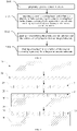
-
FIG. 1 is a schematic diagram of a cross-sectional structure of an atomization core according to an embodiment of the present disclosure. -
FIG. 2 is a schematic diagram of a cross-sectional structure of the atomization core inFIG. 1 taken along a line I-I. -
FIG. 3 is an enlarged partial view of a cross-sectional structure of an atomization core according to another embodiment of the present disclosure. -
FIG. 4 is a schematic flowchart of a preparation method of an atomization core according to an embodiment of the present disclosure. -
FIG. 5 is a schematic flowchart of processing corresponding to the preparing process inFIG. 4 . -
FIG. 6 is a schematic flowchart of step S 105 inFIG. 4 . -
FIG. 7 is a schematic flowchart of a preparation method of an atomization core according to another embodiment of the present disclosure. -
FIG. 8 is a schematic flowchart of processing corresponding to the preparing process inFIG. 7 . - The technical solutions in the embodiments of the present disclosure are clearly and thoroughly described below with reference to the accompanying drawings in the embodiments of the present disclosure. Apparently, the described embodiments are merely some but not all of the embodiments of the present disclosure. All other embodiments obtained by a person of ordinary skills in the art based on the embodiments of the present disclosure without creative efforts shall fall within the protection scope of the present disclosure.
- Referring to
FIG. 1, FIG. 1 is a schematic diagram of a cross-sectional structure of an atomization core according to an embodiment of the present disclosure. The present disclosure provides anatomization core 100 of an electronic atomization device, and theatomization core 100 includes a porousceramic substrate 10, aceramic covering layer 20, and aheating film 30. Theceramic covering layer 20 is combined or bonded on a surface of the porousceramic substrate 10, and theheating film 30 is combined or bonded on a surface of the ceramic coveringlayer 20 away from the porousceramic substrate 10. A porosity of the ceramic coveringlayer 20 is less than that of the porousceramic substrate 10, and a plurality of throughholes 21 are defined in theceramic covering layer 20. - The porosity refers to a ratio of a total volume of micropores in a porous medium to a total volume of the porous medium. The
ceramic covering layer 20 being combined or bonded on a surface of the porousceramic substrate 10 means that, theceramic covering layer 20 is combined on a surface, which is closer to a heating component, of the porousceramic substrate 10, to prevent a direct contact between the porousceramic substrate 10 and the heating component. As shown inFIG. 1 , in this embodiment, theceramic covering layer 20 is combined on an upper surface of the porousceramic substrate 10. - In some embodiments of the present disclosure, the ceramic covering
layer 20 with a porosity less than that of the porousceramic substrate 10, is combined on a surface of the porousceramic substrate 10 closer to a heating component. In this case, since the ceramic coveringlayer 20 with a less porosity has a greater density and no powder-falling phenomenon will occur, thus the powder-falling phenomenon of theatomization core 100 can be avoided. In addition, the ceramic coveringlayer 20 with a less porosity can isolate precipitates of heavy metal substance inside the porousceramic substrate 10, so that the heavy metal substance can be prevented from being entrained into the airflow during the inhaling process, and safety performance of the electronic atomization device can be improved. - In some embodiments, a material for making the porous
ceramic substrate 10 may be zirconium oxide, silicon oxide, aluminum oxide, mullite and the like, and a material for making theceramic covering layer 20 may be zirconium oxide, silicon oxide, aluminum oxide, silicon carbide, mullite and the like. The material of the porousceramic substrate 10 and the material of the ceramic coveringlayer 20 may be of the same type or different types. The types of the material of the porousceramic substrate 10 and the material of the ceramic coveringlayer 20 are not limited in the embodiments of the present disclosure. - In some embodiments, the porosity of the porous
ceramic substrate 10 is in the range of 40% to 80%. A value of the porosity may be adjusted according to composition of E-liquid. For example, when the E-liquid has a relatively great viscosity, a relatively great porosity is selected to ensure a drainage or liquid guiding effect. - In some embodiment, the porosity of the porous
ceramic substrate 10 is in the range of 50% to 60%. By controlling the porosity of the porousceramic substrate 10 to be within the range of 50% to 60%, good liquid guiding efficiency of the porousceramic substrate 10 is ensured, and dry burning phenomenon caused by poor circulation of the E-liquid can be prevented, thereby improving an atomizing effect. The porousceramic substrate 10 can be further prevented from guiding liquid at an excessively great velocity. The excessively great liquid guiding velocity can make the liquid difficult to be locked, and a probability of liquid leakage is increased. - In some embodiments, an average pore size of micro-pores in the porous
ceramic substrate 10 is in the range of 10 µm to 40 µm. For example, the average pore size may be 10 µm, 15 µm, 20 µm, 25 µm, 30 µm, 35 µm, 40 µm or the like, which is not specifically limited in the embodiments of the present disclosure. - According to the foregoing embodiments, by setting pore sizes of the micro-pores with suitable sizes and uniform distribution, liquid guiding of the porous
ceramic substrate 10 may be uniform, thereby achieving a better atomizing effect. - In some embodiments, a thickness of the porous
ceramic substrate 10 is in the range of 1 mm to 4 mm. The thickness of the porousceramic substrate 10 refers to a length of the porousceramic substrate 10 in a stacking direction of the porousceramic substrate 10 and theceramic covering layer 20. In this embodiment, the stacking direction of the porousceramic substrate 10 and theceramic covering layer 20 is a direction X shown inFIG. 1 . The thickness H of the porousceramic substrate 10 in the direction X is in the range of 1 mm to 4 mm. By providing the porousceramic substrate 10 with a suitable thickness, a liquid guiding path can be shortened, and liquid transmission may be fluent. Dry burning can also be prevented. - In some embodiments, the thickness H of the porous
ceramic substrate 10 in the direction X may be 1 mm, 1.5 mm, 2 mm, 2.5 mm, 3 mm, 3.5 mm, 4 mm and the like, which is not specifically limited in the embodiments of the present disclosure. - In some embodiments, the porosity of the
ceramic covering layer 20 is in the range of 10% to 20%. In thesame atomization core 100, the porosity of theceramic covering layer 20 is less than that of the porousceramic substrate 10, so that a denseceramic covering layer 20 is formed on the surface of the porousceramic substrate 10. In an embodiment, the porosity of theceramic covering layer 20 may be in the ranges of 10% to 18%, 10% to 16%, 10% to 14%, 10% to 12%, 12% to 18%, 12% to 16%, 12% to 14%, 14% to 16%, 14% to 18%, 16% to 18% and the like. In another embodiment, the porosity of the porousceramic substrate 10 is in the range of 50% to 60%, and the porosity of theceramic covering layer 20 is in the range of 14% to 16%. - In some embodiments, a thickness of the
ceramic covering layer 20 is in the range of 0.05 mm to 0.2 mm. The thickness of theceramic covering layer 20 refers to a length of theceramic covering layer 20 in the stacking direction of the porousceramic substrate 10 and theceramic covering layer 20. In this embodiment, the stacking direction of the porousceramic substrate 10 and theceramic covering layer 20 is the direction X shown inFIG. 1 , and a thickness R of theceramic covering layer 20 in the direction X is in the range of 0.05 mm to 0.2 mm. For example, the thickness R of theceramic covering layer 20 in the direction X is 0.05 mm, 0.07 mm, 0.09 mm, 0.11 mm, 0.13 mm, 0.15 mm, 0.17 mm, 0.2 mm and the like, which is not specifically limited in the embodiments of the present disclosure. - In some embodiments, a powder size or power granularity of the material for making the
ceramic covering layer 20 is in the range of 0.1 µm to 5 µm. The powder size is also referred to as a particle size, which refers to a scale of a space occupied by a particle. For a spherical particle, the powder size is a single parameter, namely, a diameter D. For a particle of an irregular shape, the powder size may be expressed by (any) projection height H, a maximum length M, a horizontal width W, a diameter of a sphere with a same volume, a diameter D of a sphere with a same surface area and the like. - In some embodiments, the powder size of the material for making the
ceramic covering layer 20 is 0.1 µm, 0.5 µm, 1 µm, 1.5 µm, 2 µm, 2.5 µm, 3 µm, 3.5 µm, 4 µm and the like, which is not specifically limited in the embodiments of the present disclosure. - According to the foregoing optional embodiments, by providing the
ceramic covering layer 20 with a suitable thickness, setting pore sizes of micro-pores with suitable sizes and uniform distribution, and providing a raw material with a relatively small powder size, theceramic covering layer 20 can effectively isolate precipitates of heavy metal substance. - Further, as shown in
FIG. 1 and FIG. 2, FIG. 2 is a schematic diagram of a cross-sectional structure of the atomization core inFIG. 1 taken along a line I-I. A diameter of eachhole 21 defined in theceramic covering layer 20 is in the range of 5 µm to 50 µm. For example, the diameter of thehole 21 may be 5 µm, 10 µm, 15 µm, 20 µm, 25 µm, 30 µm, 35 µm, 40 µm, 45 µm, 50 µm and the like, which is not specifically limited in the embodiments of the present disclosure. It should be noted that, theholes 21 in theceramic covering layer 20 are not the micro-pores in the porous medium, and the existence of theholes 21 does not affect the porosity of theceramic covering layer 20. In other words, the porosity of theceramic covering layer 20 is irrelevant to the plurality ofholes 21 defined in theceramic covering layer 20. - In some embodiments, the plurality of
holes 21 are defined in theceramic covering layer 20, and eachhole 21 penetrates theceramic covering layer 20 in the stacking direction of the porousceramic substrate 10 and theceramic covering layer 20. By defining the plurality of throughholes 21 in theceramic covering layer 20,the liquid guiding of theceramic covering layer 20 may be facilitated. - In some embodiments, diameters of the plurality of
holes 21 defined in the sameceramic covering layer 20 may be the same or may be different, which is not specifically limited in the embodiments of the present disclosure. - In this embodiment, as shown in
FIG. 2 , the plurality ofholes 21 are defined in theceramic covering layer 20 in an array. In another embodiment, the plurality ofholes 21 may be alternatively distributed in an annular, and an arrangement manner of the plurality ofholes 21 is not specifically limited in the embodiments of the present disclosure. - In some embodiments, the
hole 21 defined in theceramic covering layer 20 is a circular hole. In other embodiments, the shape of thehole 21 is a rectangle, an ellipse, a triangle, a diamond, a regular or irregular polygon and the like, which is not specifically limited in the embodiments of the present disclosure. - Further, a ratio of a total opening area of the plurality of
holes 21 to a cross-sectional area of theceramic covering layer 20 perpendicular to an extending direction of theholes 21 is in the range of 5% to 15%. For example, the ratio of the total opening area of the plurality ofholes 21 to the cross-sectional area of theceramic covering layer 20 perpendicular to the extending direction of theholes 21 is in the range of 5% to 12%, 5% to 10%, 5% to 8%, 7% to 12%, 7% to 10%, 9% to 12%, 10% to 12%, 7% to 15%, 9% to 15%, 12% to 15%, 14% to 15% and the like, which is not specifically limited in the embodiments of the present disclosure. - Specifically, in this embodiment, as shown in
FIG. 1 , the extending direction of thehole 21 is an axial direction of the circular hole, and the axial direction of the circular hole is parallel to the direction X. Therefore, the cross section of theceramic covering layer 20 perpendicular to the extending direction of theholes 21 is a cross section of theceramic covering layer 20 perpendicular to the direction X, namely, the cross section shown inFIG. 2 . The total opening area of the plurality ofholes 21 refers to an area of blank regions shown in the figure, and the ratio of the total opening area of the plurality ofholes 21 to the cross-sectional area of theceramic covering layer 20 perpendicular to the extending direction of theholes 21 refers to a ratio of the area of the blank regions inFIG. 2 to an area of the entire cross section. - Further, as shown in
FIG. 1 , theheating film 30 is combined on the surface of theceramic covering layer 20 away from the porousceramic substrate 10. Theheating film 30 is configured to be electrically connected to an electrode and generate heat to atomize the E-liquid. - In some embodiments, a thickness of the
heating film 30 is in the range of 2 µm to 10 µm. The thickness of theheating film 30 refers to a length of theheating film 30 in the stacking direction of the porousceramic substrate 10 and theceramic covering layer 20. As shown inFIG. 1 , the thickness of theheating film 30 is L. The thickness L may be specifically 2 µm, 3 µm, 4 µm, 5 µm, 6 µm, 7 µm, 8 µm, 9 µm, 9.5 µm, 10 µm and the like, which is not specifically limited in the embodiments of the present disclosure. - In some embodiments, as shown in
FIG. 3, FIG. 3 is an enlarged partial view of a cross-sectional structure of an atomization core according to another embodiment of the present disclosure. Theheating film 30 includes afirst covering film 32 and asecond covering film 34. Thefirst covering film 32 is stacked on the surface of theceramic covering layer 20 away from the porousceramic substrate 10, and thesecond covering film 34 is stacked on a surface of thefirst covering film 32 away from theceramic covering layer 20. - The
first covering film 32 can be made of metal or alloy. To increase the bonding force between thefirst covering film 32 and the porousceramic substrate 10, thefirst covering film 32 may be made of a material that can be stably bonded to the porousceramic substrate 10. For example, thefirst covering film 32 can be made of titanium, zirconium, titanium-aluminum alloy, titanium-zirconium alloy, titanium-molybdenum alloy, titanium-niobium alloy, iron-aluminum alloy, tantalum-aluminum alloy and the like. - A titanium-zirconium alloy film made of the titanium-zirconium alloy is a local dense film, but the porous
ceramic substrate 10 is in itself a porous structure. As a result, the titanium-zirconium alloy film formed on the surface of the porousceramic substrate 10 also has a porous continuous structure. Pore size of the titanium-zirconium alloy film is slightly less than the pore size of the micro-pores on the surface of the porousceramic substrate 10. - Further, the stability of titanium and zirconium of the titanium-zirconium alloy film in the air is relatively poor under a high temperature. Zirconium can easily adsorb hydrogen, nitrogen, and oxygen. Zirconium and titanium have enhanced gas adsorption after being alloyed. Therefore, when an electrode is prepared subsequently, due to the gas adsorption of the titanium-zirconium alloy, during a high temperature sintering (higher than 300 °C), intense oxidation reaction can occur, causing an abrupt change in the resistance of the
first covering film 32. To prevent thefirst covering film 32 from contacting with air, one protection layer needs to be provided on a surface of thefirst covering film 32. Thesecond covering film 34 can be used as the protection layer. - The
second covering film 34 can also be made of metal or alloy. To prevent thefirst covering film 32 from contacting with air and being oxidized to cause an abrupt change in the resistance thereof, thesecond covering film 34 should be made of a material with stronger resistance to oxidation. For example, thesecond covering film 34 can be made of platinum, palladium, palladium-copper alloy, gold-silver-platinum alloy, gold-silver alloy, palladium-silver alloy, gold-platinum alloy and the like. - A protection layer made of silver or platinum is relatively loose and has a relatively low density, which can hardly isolate or insulate air completely. Gold can protect the titanium-zirconium alloy film well. However, to make a dense protection layer, a thickness of about 100 nm or larger is required, which can greatly reduce the electrical resistance of the entire heating component and brings a great cost. Therefore, in this embodiment, the gold-silver alloy is used, so that the density of the gold protection layer is retained while the costs are reduced. Electrical resistivity of the gold-silver alloy is increased by ten times after gold and silver are alloyed according to a specific ratio, the control of the electrical resistance of the entire heating component is thereby facilitated.
- The present disclosure further provides a preparation method of an atomization core of an electronic atomization device, and the
atomization core 100 in the foregoing embodiments may be made by the preparation method. As shown inFIG. 4 and FIG. 5, FIG. 4 is a schematic flowchart of a preparation method of the atomization core according to an embodiment of the present disclosure, andFIG. 5 is a schematic flowchart of processing corresponding to the preparing process inFIG. 4 . The preparation method of theatomization core 100 includes operations at blocks shown inFIG. 4 . - At block S101: the method prepares a porous
ceramic substrate 10. - First, a raw material for making the porous
ceramic substrate 10 is made into a first tape-casting slurry. The raw material for making the porousceramic substrate 10 may be zirconium oxide, silicon oxide, aluminum oxide, mullite and the like, and at least one of the foregoing raw materials is mixed to form the first tape-casting slurry. - The first tape-casting slurry is then made into the porous
ceramic substrate 10 by a tape-casting process. In addition, a tape-casting time can be controlled to cause a thickness of the porousceramic substrate 10 to be in the range of 1 mm to 4 mm. - At block S102: the method prepares a
ceramic covering layer 20, and defines a plurality of holes penetrating theceramic covering layer 20 in the ceramic covering layer 20.The porosity of theceramic covering layer 20 is less than that of the porousceramic substrate 10. - First, a raw material for making the
ceramic covering layer 20 is made into a second tape-casting slurry. The material for making theceramic covering layer 20 may be zirconium oxide, silicon oxide, aluminum oxide, silicon carbide, mullite and the like, and a powder size of the material for making theceramic covering layer 20 is in the range of 0.1 µm to 5 µm. At least one of the foregoing raw materials is mixed to form the second tape-casting slurry. - In some embodiments, the second tape-casting slurry can be then made into the
ceramic covering layer 20 by the tape-casting process. In addition, a casting time can be controlled to cause the thickness of theceramic covering layer 20 to be in the range of 0.05 mm to 0.2 mm. - Alternatively, in another embodiment, the second tape-casting slurry can be pressed into the
ceramic covering layer 20 by a dry-pressing process, which is not specifically limited in the embodiments of the present disclosure. - After the
ceramic covering layer 20 is prepared, a plurality of holes penetrating theceramic covering layer 20 need to be further defined in theceramic covering layer 20. A diameter of eachhole 21 is in the range of 5 µm to 50 µm, and a ratio of a total area of the plurality ofholes 21 to a cross-sectional area of theceramic covering layer 20 perpendicular to an extending direction of theholes 21 is in the range of 5% to 15%. - Specifically, the plurality of
holes 21 penetrating theceramic covering layer 20 can be directly defined in theceramic covering layer 20 through laser drilling, computerized numerical control (CNC) precision drilling, or selective corrosion drilling. By directly defining the through holes penetrating theceramic covering layer 20 in theceramic covering layer 20, the drilling process is simple, and the holes 21in the formedatomization core 100 have relatively high depth consistency. - In some embodiments, diameters of the plurality of
holes 21 defined in the sameceramic covering layer 20 may be the same or may be different. The shape of thehole 21 defined in theceramic covering layer 20 may be a circle, a rectangle, an ellipse, a triangle, a diamond, a regular or irregular polygon and the like, which is not specifically limited in the embodiments of the present disclosure. - In the foregoing embodiments, the porous
ceramic substrate 10 is first prepared, and theceramic covering layer 20 is then prepared. It should be understood that, in another embodiment, theceramic covering layer 20 can be first prepared, and the porousceramic substrate 10 is then prepared. Alternatively, in still another embodiment, theceramic covering layer 20 and the porousceramic substrate 10 are prepared at the same time, which is not specifically limited in the embodiments of the present disclosure. - After operations S101 and S102 are performed to obtain the porous
ceramic substrate 10 and theceramic covering layer 20, the following operations are performed. - At block S103: the method stacks and combines the porous
ceramic substrate 10 and theceramic covering layer 20 together to form an integral structure. - Specifically, in an embodiment, the
ceramic covering layer 20 can be stacked on one side of the porousceramic substrate 10, and theceramic covering layer 20 and the porousceramic substrate 10 are connected and fixed through bonding. - In some embodiments, the
ceramic covering layer 20 can be stacked on one side of the porousceramic substrate 10, and the porousceramic substrate 10 and theceramic covering layer 20 are connected through sintering. - The sintering refers to a process in which solid particles of a ceramic green body are mutually bonded under a high temperature (not higher than a melting point). As crystalline grains grow, gaps (pores) and grain boundaries are gradually decreased, and through mass transfer, a total volume of the ceramic green body shrinks and the density thereof is increased. Finally, the ceramic green body becomes a dense polycrystalline sintered compact with a type of microscopic structure. In this embodiment, the
ceramic covering layer 20 and the porousceramic substrate 10 are connected through sintering, and no harmful material is generated, so that the safety performance of theatomization core 100 can be improved. - Referring to
FIG. 4 and FIG. 5 , in this embodiment, after operation S103 is performed to obtain the porousceramic substrate 10 and theceramic covering layer 20 that form an integral structure, the method further includes the following operation. - At block S104: the method forms a
heating film 30 on a surface of theceramic covering layer 20 away from the porousceramic substrate 10. - A thickness of the heating film is in the range of 2 µm to 10 µm. In some embodiments, the
heating film 30 may be formed on theceramic covering layer 20 through physical vapor deposition (PVD), electroplating, electro-deposition, ion plating, coating, chemical vapor deposition (CVD) and the like. A uniformly distributedheating film 30 with a relatively small thickness and a relatively large area may be formed in any of the foregoing manners. In this way, when theheating film 30 is electrically connected to an electrode, theheating film 30 generates heat uniformly and has a large heating area and high heat utilization ratio. In addition, precipitation of heavy metal substance inside theatomization core 100 can be greatly reduced, thereby further improving the safety performance. - In some embodiments, as shown in
FIG. 3 andFIG. 6, FIG. 6 is a schematic flowchart of operation S105 inFIG. 4 . The operation of forming aheating film 30 on a surface of theceramic covering layer 20 away from the porousceramic substrate 10 includes the following operation at blocks shown inFIG. 6 . - At block S201: the method forms a
first covering film 32 on the surface of theceramic covering layer 20 away from the porousceramic substrate 10. - The
first covering film 32 can be made of metal or alloy. Thefirst covering film 32 can be made of a material with relatively strong bonding force to the porousceramic substrate 10. For example, thefirst covering film 32 can be made of titanium, zirconium, titanium-aluminum alloy, titanium-zirconium alloy, titanium-molybdenum alloy, titanium-niobium alloy, iron-aluminum alloy, tantalum-aluminum alloy and the like. - At block S202: the method forms a
second covering film 34 on a surface of thefirst covering film 32 away from theceramic covering layer 20. - The
second covering film 34 can also be made of metal or alloy. Thesecond covering film 34 may be made of a material with relatively strong resistance to oxidation. For example, thesecond covering film 34 can be platinum, palladium, palladium-copper alloy, gold-silver-platinum alloy, gold-silver alloy, palladium-silver alloy, gold-platinum alloy and the like. - In some embodiments, the
first covering film 32 and thesecond covering film 34 can be sequentially formed on the surface of theceramic covering layer 20 away from the porousceramic substrate 10 through PVD, CVD, electroplating, electro-deposition, ion plating, coating and the like. Thefirst covering film 32 and thesecond covering film 34 that are formed in the foregoing manners have a relatively small thickness and a relatively large area, and are uniformly distributed, so that when theheating film 30 is electrically connected to an electrode, theheating film 30 generates heat uniformly, and has a large heating area and high heat utilization ratio. In addition, precipitation of heavy metal substance inside theatomization core 100 can be greatly reduced, thereby further improving the safety performance. - In another embodiment, referring to
FIG. 7 andFIG. 8 ,FIG. 7 is a schematic flowchart of a preparation method of an atomization core according to another embodiment of the present disclosure, andFIG. 8 is a schematic flowchart of processing corresponding to the preparing process inFIG. 7 . The preparation method of theatomization core 100 in this embodiment includes the following operations at blocks shown inFIG. 7 . - At block S301: the method prepares a porous
ceramic substrate 10. - At block S302: the method prepares a
ceramic covering layer 20. A porosity of theceramic covering layer 20 is less than that of the porousceramic substrate 10. - At block S303: the method stacks and combines the porous
ceramic substrate 10 and theceramic covering layer 20 together to form an integral structure. - At block S304: the method defines a plurality of
holes 21 in theceramic covering layer 20. - At block S305: the method defines a
heating film 30 on a surface of theceramic covering layer 20 away from the porousceramic substrate 10. - Operation S301 is substantially the same as operation S101 in the foregoing embodiments, operation S303 is substantially the same as operation S103 in the foregoing embodiments, and operation S305 is substantially the same as operation S104 in the foregoing embodiments. Refer can be made to the description in the foregoing embodiments, and details are not described herein again. A difference between this embodiment and the foregoing embodiments lies in that, in this embodiment, the plurality of
holes 21 in theceramic covering layer 20 are not defined while theceramic covering layer 20 is being prepared, but are defined after the porousceramic substrate 10 and theceramic covering layer 20 are combined into an integral structure, and are defined through drilling on a side where theceramic covering layer 20 is located. - In this embodiment, during the drilling process, first, it is necessary to set a drilling depth to be equal to a thickness of the
ceramic covering layer 20, and then the drilling is initiated on the side where theceramic covering layer 20 is located, to define a plurality of blind holes in the porousceramic substrate 10 and theceramic covering layer 20 that are combined into an integral structure. A drilling manner and a size of the hole are the same as those in the foregoing embodiments, and reference may be made to the description in the foregoing embodiments. - The present disclosure further provides an electronic atomization device, including a liquid storage cavity configured to store E-liquid and an atomization core. The E-liquid in the liquid storage cavity is capable of being transmitted to the ceramic covering layer through the porous ceramic substrate.
- A structure of the atomization core in this embodiment is the same as the structure of the atomization core in the foregoing embodiments. Reference can be made to the description in the foregoing embodiments, and details are not described herein again.
- In summary, a person skilled in the art can easily understand that, a
ceramic covering layer 20 whose porosity is less than that of a porousceramic substrate 10 is combined on a surface, which is closer to a heating component, of the porousceramic substrate 10, so that powder falling of the atomization core can be avoided, because theceramic covering layer 20 with a lower porosity has a greater density and prevents powder falling. In addition, theceramic covering layer 20 with a less porosity can isolate precipitates of heavy metal substance inside the porousceramic substrate 10, so that the heavy metal substance can be prevented from being entrenched into airflow during inhaling, thereby improving safety performance of the electronic atomization device. - The foregoing descriptions are merely embodiments of the present disclosure, and the protection scope of the present disclosure is not limited thereto. All equivalent structure or process changes made according to the content of this specification and accompanying drawings in the present disclosure or by directly or indirectly applying the present disclosure in other related technical fields shall fall within the protection scope of the present disclosure.
Claims (17)
- An atomization core of an electronic atomization device, characterized by comprising:a porous ceramic substrate, a ceramic covering layer, and a heating film, wherein the ceramic covering layer is combined on a surface of the porous ceramic substrate, the heating film is combined on a surface of the ceramic covering layer away from the porous ceramic substrate,a porosity of the ceramic covering layer is less than that of the porous ceramic substrate, anda plurality of through holes are defined in the ceramic covering layer.
- The atomization core as claimed in claim 1, wherein the porosity of the porous ceramic substrate is in a range of 40% to 80%; and/oran average pore size of micro-pores in the porous ceramic substrate is in a range of 10 µm to 40 µm; and/ora material for making the porous ceramic substrate is zirconium oxide, silicon oxide, aluminum oxide, or mullite; and/ora thickness of the porous ceramic substrate is in a range of 1 mm to 4 mm.
- The atomization core as claimed in claim 1, wherein the porosity of the ceramic covering layer is in a range of 10% to 20%; and/ora material for making the ceramic covering layer is zirconium oxide, silicon oxide, aluminum oxide, silicon carbide, or mullite; and/ora thickness of the ceramic covering layer is in a range of 0.05 mm to 0.2 mm; and/ora powder size of the material for making the ceramic covering layer is in a range of 0.1 µm to 5 µm.
- The atomization core as claimed in claim 1, wherein a diameter of each of the plurality of through holes is in a range of 5 µm to 50 µm.
- The atomization core as claimed in claim 4, wherein a ratio of a total opening area of the plurality of through holes to a cross-sectional area of the ceramic covering layer perpendicular to an extending direction of the through holes is in a range of 5% to 15%.
- The atomization core as claimed in claim 1, wherein a powder size of a material for making the ceramic covering layer is in a range of 0.1 µm to 5 µm.
- The atomization core as claimed in claim 1, wherein the heating film is made of metal or alloy; and/or
a thickness of the heating film is in a range of 2 µm to 10 µm. - The atomization core as claimed in claim 1, wherein the heating film comprises a first covering film and a second covering film; and the first covering film is stacked on the surface of the ceramic covering layer away from the porous ceramic substrate, and the second covering film is stacked on a surface of the first covering film away from the ceramic covering layer.
- The atomization core as claimed in claim 8, wherein the first covering film and the second covering film are made of metal or alloy.
- A preparation method of an atomization core of an electronic atomization device, characterized by comprising:preparing a porous ceramic substrate;preparing a ceramic covering layer, and defining, in the ceramic covering layer, a plurality of holes penetrating the ceramic covering layer, wherein a porosity of the ceramic covering layer is less than that of the porous ceramic substrate;stacking and combining the porous ceramic substrate and the ceramic covering layer to form an integral structure; andforming a heating film on a surface of the ceramic covering layer away from the porous ceramic substrate.
- The preparation method as claimed in claim 10, wherein the preparing the porous ceramic substrate comprises:making a first tape-casting slurry from a raw material for forming the porous ceramic substrate; andmaking the porous ceramic substrate through a tape-casting process, wherein a thickness of the porous ceramic substrate is in a range of 1 mm to 4 mm.
- The preparation method as claimed in claim 10, wherein the preparing the ceramic covering layer comprise:making a second tape-casting slurry from a raw material for forming the ceramic covering layer, wherein a powder size of the raw material for forming the ceramic covering layer is in a range of 0.1 µm to 5 µm; andmaking the ceramic covering layer through a tape-casting process or a dry-pressing process, wherein a thickness of the ceramic covering layer is in a range of 0.05 mm to 0.2 mm.
- The preparation method as claimed in claim 10, wherein the stacking and combining the porous ceramic substrate and the ceramic covering layer to form the integral structure comprises:
connecting the porous ceramic substrate to the ceramic covering layer through bonding or sintering. - The preparation method as claimed in claim 10, wherein the forming the heating film on the surface of the ceramic covering layer away from the porous ceramic substrate comprises:
forming the heating film on the surface of the ceramic covering layer away from the porous ceramic substrate through physical vapor deposition (PVD), chemical vapor deposition (CVD), electroplating, electro-deposition, ion plating, or coating, a thickness of the heating film is in a range of 2 µm to 10 µm. - The preparation method as claimed in claim 10, wherein the forming the heating film on the surface of the ceramic covering layer away from the porous ceramic substrate comprises:forming a first covering film on the surface of the ceramic covering layer away from the porous ceramic substrate through physical vapor deposition (PVD), chemical vapor deposition (CVD), electroplating, electro-deposition, ion plating, or coating; andforming a second covering film on a surface of the first covering film away from the ceramic covering layer through PVD, CVD, electroplating, electro-deposition, ion plating, or coating, wherein the first covering film and the second covering film form the heating film.
- The preparation method as claimed in claim 15, wherein the first covering film and the second covering film are made of metal or alloy.
- An electronic atomization device, characterized by comprising a liquid storage cavity configured to store E-liquid and the atomization core as claimed in claim 1, wherein the E-liquid in the liquid storage cavity is capable of being transmitted to the ceramic covering layer through the porous ceramic substrate.
Applications Claiming Priority (2)
| Application Number | Priority Date | Filing Date | Title |
|---|---|---|---|
| CN201911214936.3A CN111053291B (en) | 2019-12-02 | 2019-12-02 | Electronic atomization device, atomization core and preparation method thereof |
| PCT/CN2020/122524 WO2021109740A1 (en) | 2019-12-02 | 2020-10-21 | Electronic atomization device, atomization core and preparation method therefor |
Publications (3)
| Publication Number | Publication Date |
|---|---|
| EP4070673A1 true EP4070673A1 (en) | 2022-10-12 |
| EP4070673A4 EP4070673A4 (en) | 2023-01-25 |
| EP4070673B1 EP4070673B1 (en) | 2025-12-24 |
Family
ID=70299471
Family Applications (1)
| Application Number | Title | Priority Date | Filing Date |
|---|---|---|---|
| EP20895239.0A Active EP4070673B1 (en) | 2019-12-02 | 2020-10-21 | Electronic atomization device, atomization core and preparation method therefor |
Country Status (4)
| Country | Link |
|---|---|
| US (1) | US20220279855A1 (en) |
| EP (1) | EP4070673B1 (en) |
| CN (1) | CN111053291B (en) |
| WO (1) | WO2021109740A1 (en) |
Cited By (2)
| Publication number | Priority date | Publication date | Assignee | Title |
|---|---|---|---|---|
| WO2024183667A1 (en) * | 2023-03-03 | 2024-09-12 | Shanghai QV Technologies Co., Ltd. | Atomization core for electronic atomizer and its processing method |
| WO2024200744A1 (en) * | 2023-03-29 | 2024-10-03 | Philip Morris Products S.A. | Ceramic heating member |
Families Citing this family (34)
| Publication number | Priority date | Publication date | Assignee | Title |
|---|---|---|---|---|
| CN112251723B (en) * | 2019-07-04 | 2022-05-03 | 深圳麦克韦尔科技有限公司 | Heating element, preparation method thereof and electronic smoking set |
| CN111053291B (en) * | 2019-12-02 | 2025-04-25 | 深圳麦克韦尔科技有限公司 | Electronic atomization device, atomization core and preparation method thereof |
| CN111700310A (en) * | 2020-05-22 | 2020-09-25 | 深圳陶陶科技有限公司 | Porous gradient ceramic heating element for liquid atomizer and preparation method thereof |
| PH12022553418A1 (en) * | 2020-06-18 | 2024-04-22 | Philip Morris Products Sa | Heater assembly having fluid permeable heater with directly deposited transport material |
| TWI741822B (en) | 2020-10-07 | 2021-10-01 | 聚鼎科技股份有限公司 | Vaporizing apparatus and vaporizer thereof |
| CN112315039B (en) * | 2020-11-18 | 2024-11-22 | 深圳麦克韦尔科技有限公司 | Ceramic heating element, atomizer, electronic atomization device and preparation method of ceramic heating element |
| CN114532608A (en) * | 2020-11-24 | 2022-05-27 | 深圳雾芯科技有限公司 | Atomizing core reaches atomizer and electron cigarette including it |
| CN114617299A (en) * | 2020-12-11 | 2022-06-14 | 常州市派腾电子技术服务有限公司 | Atomizing core, atomizer, aerosol generating device and atomizing core processing method |
| CN115104778B (en) * | 2021-03-19 | 2025-03-07 | 比亚迪股份有限公司 | Atomizer, method for making atomizer, and electronic cigarette |
| CN114794565A (en) * | 2021-07-05 | 2022-07-29 | 深圳麦克韦尔科技有限公司 | Heating body, atomizing component and electronic atomizing device |
| CN114794569B (en) * | 2021-07-23 | 2025-09-05 | 深圳麦克韦尔科技有限公司 | Atomizing core, atomizer and electronic atomizing device |
| CN113624048A (en) * | 2021-08-13 | 2021-11-09 | 合肥领途材料科技合伙企业(有限合伙) | Porous ceramic with straight pore gradient structure, capillary core and preparation method thereof |
| CN116217269B (en) * | 2021-12-03 | 2024-07-12 | 深圳麦克韦尔科技有限公司 | Porous ceramic, modification liquid for modifying inner surface of porous ceramic, preparation method and application thereof |
| WO2023098260A1 (en) * | 2021-12-04 | 2023-06-08 | 常州市派腾电子技术服务有限公司 | Atomizing core, atomizer, and aerosol generation device |
| CN114346258A (en) * | 2021-12-28 | 2022-04-15 | 深圳市吉迩科技有限公司 | Preparation method of atomizing core and atomizer |
| CN116406825B (en) * | 2021-12-31 | 2026-05-05 | 深圳市合元科技有限公司 | Porous bodies, atomizers and electronic atomization devices |
| CN116439430A (en) * | 2022-01-07 | 2023-07-18 | 江门思摩尔新材料科技有限公司 | Heating component, preparation method thereof, atomizer and electronic atomization device |
| CN114287676B (en) * | 2022-01-17 | 2024-12-24 | 海宁新纳陶科技有限公司 | Ceramic atomizing core with metal coating layer and preparation method thereof |
| CN114271550A (en) * | 2022-01-20 | 2022-04-05 | 美满芯盛(杭州)微电子有限公司 | Silicon-based heating atomization core for liquid atomization and manufacturing method thereof |
| GB202206234D0 (en) * | 2022-04-28 | 2022-06-15 | Nicoventures Trading Ltd | Heater assembly and method |
| EP4298932B1 (en) * | 2022-05-13 | 2024-09-04 | Shenzhen Smoore Technology Limited | Heat generating element, atomizing assembly, and electronic atomizing device |
| CN114831358B (en) * | 2022-05-20 | 2025-08-19 | 深圳市赛尔美电子科技有限公司 | Heating component of atomization device and preparation method thereof |
| CN117796568A (en) * | 2022-09-23 | 2024-04-02 | 深圳市合元科技有限公司 | Atomizer, electronic atomization device, porous body and preparation method |
| CN115534493B (en) * | 2022-10-20 | 2024-06-21 | 深圳市尚进电子科技有限公司 | Micro-grid atomizing sheet based on FPC flexible circuit board and manufacturing process thereof |
| CN115721053A (en) * | 2022-11-19 | 2023-03-03 | 深圳市卓尔悦电子科技有限公司 | Atomizing core, atomizer, aerosol generating device and atomizing core preparation method |
| CN115976483A (en) * | 2022-12-13 | 2023-04-18 | 深圳市吉迩技术有限公司 | A high-power ceramic heating body and its preparation method |
| CN116082066A (en) * | 2022-12-28 | 2023-05-09 | 深圳市基克纳科技有限公司 | Ceramic substrate-metal thin film product and its preparation method and electronic atomizer |
| CN115918982A (en) * | 2022-12-29 | 2023-04-07 | 深圳市吉迩科技有限公司 | Porous ceramic heating element and its preparation method |
| CN119036947B (en) * | 2023-05-29 | 2025-09-16 | 佛山市顺德区美的电热电器制造有限公司 | Panels and appliances |
| WO2025016412A1 (en) * | 2023-07-18 | 2025-01-23 | Shanghai QV Technologies Co., Ltd. | Heating element, atomization device and atomization equipment |
| CN117303943B (en) * | 2023-09-27 | 2025-10-03 | 深圳市吉嘉新材料科技有限公司 | Conductive ceramic and preparation method thereof |
| CN117645498A (en) * | 2023-10-15 | 2024-03-05 | 东莞仁海科技股份有限公司 | Rule-side array hole ceramic for electronic cigarette and preparation method thereof |
| CN117417202B (en) * | 2023-10-30 | 2026-01-06 | 深圳市吉嘉新材料科技有限公司 | Method for preparing ceramic substrate, atomizing core and aerosol forming device |
| CN117447193B (en) * | 2023-10-30 | 2025-11-18 | 武汉利之达科技股份有限公司 | A modified 3D printed ceramic atomizing core substrate and its preparation method |
Family Cites Families (16)
| Publication number | Priority date | Publication date | Assignee | Title |
|---|---|---|---|---|
| KR20170102415A (en) * | 2016-01-26 | 2017-09-11 | 시아오춘 주 | Ceramic vaporizer with replaceable e-liquid storage medium and electronic cigarettes having the same |
| DE102016120803A1 (en) * | 2016-11-01 | 2018-05-03 | Hauni Maschinenbau Gmbh | An evaporator unit for an inhaler and method for controlling an evaporator unit |
| CN107006896B (en) * | 2017-05-05 | 2019-04-09 | 湖北中烟工业有限责任公司 | A kind of composite ceramic atomizer and preparation method thereof |
| CN108208938A (en) * | 2017-12-27 | 2018-06-29 | 深圳市卓力能电子有限公司 | A kind of heater and preparation method |
| DE102018105220A1 (en) * | 2018-03-07 | 2019-09-12 | Hauni Maschinenbau Gmbh | Method for producing an electrically operable radiator for an inhaler |
| CN109105958B (en) * | 2018-08-17 | 2024-07-12 | 深圳市合元科技有限公司 | Heating components, atomizing cores, atomizers and electronic cigarettes |
| EP3850967B1 (en) * | 2018-09-10 | 2024-05-29 | Shenzhen Smoore Technology Limited | Electronic cigarette, atomization assembly, and atomization component for same |
| CN109527657A (en) * | 2018-12-21 | 2019-03-29 | 深圳市合元科技有限公司 | The preparation method and electronic smoke atomizer of atomizing component |
| CN209498589U (en) * | 2019-01-05 | 2019-10-18 | 深圳市合元科技有限公司 | Atomizer and electronic cigarette |
| CN109674094A (en) * | 2019-01-26 | 2019-04-26 | 深圳市合元科技有限公司 | Electronic smoke atomizer and electronic cigarette, atomizing component preparation method |
| CN109984387A (en) * | 2019-04-22 | 2019-07-09 | 深圳市合元科技有限公司 | Atomizing component and preparation method thereof |
| CN110074463A (en) * | 2019-05-14 | 2019-08-02 | 东莞市东思电子技术有限公司 | A kind of electronic cigarette oil atomization core micropore ceramics thick film heating element and preparation method thereof |
| CN110419779B (en) * | 2019-07-15 | 2024-08-06 | 深圳市合元科技有限公司 | Electronic cigarette atomizer, electronic cigarette and preparation method of atomization component |
| CN210642434U (en) * | 2019-08-22 | 2020-06-02 | 厦门海赛米克新材料科技有限公司 | Improved structure of porous ceramic, electronic cigarette and porous ceramic atomizer |
| CN211746958U (en) * | 2019-12-02 | 2020-10-27 | 深圳麦克韦尔科技有限公司 | Electronic atomization device and atomization core thereof |
| CN111053291B (en) * | 2019-12-02 | 2025-04-25 | 深圳麦克韦尔科技有限公司 | Electronic atomization device, atomization core and preparation method thereof |
-
2019
- 2019-12-02 CN CN201911214936.3A patent/CN111053291B/en active Active
-
2020
- 2020-10-21 WO PCT/CN2020/122524 patent/WO2021109740A1/en not_active Ceased
- 2020-10-21 EP EP20895239.0A patent/EP4070673B1/en active Active
-
2022
- 2022-05-27 US US17/826,513 patent/US20220279855A1/en not_active Abandoned
Cited By (2)
| Publication number | Priority date | Publication date | Assignee | Title |
|---|---|---|---|---|
| WO2024183667A1 (en) * | 2023-03-03 | 2024-09-12 | Shanghai QV Technologies Co., Ltd. | Atomization core for electronic atomizer and its processing method |
| WO2024200744A1 (en) * | 2023-03-29 | 2024-10-03 | Philip Morris Products S.A. | Ceramic heating member |
Also Published As
| Publication number | Publication date |
|---|---|
| WO2021109740A1 (en) | 2021-06-10 |
| CN111053291A (en) | 2020-04-24 |
| CN111053291B (en) | 2025-04-25 |
| EP4070673B1 (en) | 2025-12-24 |
| EP4070673A4 (en) | 2023-01-25 |
| US20220279855A1 (en) | 2022-09-08 |
Similar Documents
| Publication | Publication Date | Title |
|---|---|---|
| EP4070673B1 (en) | Electronic atomization device, atomization core and preparation method therefor | |
| CN211746958U (en) | Electronic atomization device and atomization core thereof | |
| JP3640511B2 (en) | Nickel super fine powder | |
| WO2000048717A1 (en) | Method for manufacturing a membrane | |
| CN113245543B (en) | Copper powder, preparation method thereof and capillary core prepared from copper powder | |
| US6207038B1 (en) | Process for preparing a composite electrolyte based on BIMEVOX and the use of said compound in separating oxygen from a gas mixture | |
| CN114744221A (en) | Porous anode layer structure, preparation method thereof and fuel cell | |
| US20060196410A1 (en) | Whisker-grown body and electrochemical capacitor using the same | |
| JP5619199B2 (en) | Method for adjusting slurry viscosity and method for producing slurry | |
| JP2014534553A (en) | Accumulating member and method for producing the accumulating member | |
| KR101185323B1 (en) | Solid oxidee fuel cell cathode comprising materials coated with silver nano particle and method for manufacturing the same | |
| JP5242955B2 (en) | Method for adjusting slurry viscosity and method for producing slurry | |
| JP2848551B2 (en) | Method for producing electrolyte membrane for solid oxide fuel cell | |
| JPS60154464A (en) | Molten carbonate fuel cell | |
| JP2004342555A (en) | Electrode material for solid oxide fuel cell, method for producing the same, and solid oxide fuel cell using the same | |
| JP2001329380A (en) | Method for manufacturing porous plate material | |
| JPH0311503B2 (en) | ||
| US7195794B2 (en) | Method of making an electrolytic cell | |
| JPS63105469A (en) | Manufacture of nickel substrate for alkaline battery | |
| JP4868231B2 (en) | Porous titanium having low contact resistance and method for producing the same | |
| JP2020126738A (en) | Power storage device | |
| JP2002241996A (en) | Electroplating apparatus, plating solution holding member for electroplating apparatus, method for manufacturing copper wiring semiconductor | |
| CN118077970A (en) | Atomizer core and preparation method and application thereof | |
| JPH0349156A (en) | Fuel electrode for solid electrolyte fuel cells | |
| CN116784536A (en) | An aerosol generating device for smokeable materials and preparation method thereof |
Legal Events
| Date | Code | Title | Description |
|---|---|---|---|
| STAA | Information on the status of an ep patent application or granted ep patent |
Free format text: STATUS: THE INTERNATIONAL PUBLICATION HAS BEEN MADE |
|
| PUAI | Public reference made under article 153(3) epc to a published international application that has entered the european phase |
Free format text: ORIGINAL CODE: 0009012 |
|
| STAA | Information on the status of an ep patent application or granted ep patent |
Free format text: STATUS: REQUEST FOR EXAMINATION WAS MADE |
|
| 17P | Request for examination filed |
Effective date: 20220629 |
|
| AK | Designated contracting states |
Kind code of ref document: A1 Designated state(s): AL AT BE BG CH CY CZ DE DK EE ES FI FR GB GR HR HU IE IS IT LI LT LU LV MC MK MT NL NO PL PT RO RS SE SI SK SM TR |
|
| REG | Reference to a national code |
Ref country code: DE Ref legal event code: R079 Free format text: PREVIOUS MAIN CLASS: A24F0040400000 Ipc: H05B0003160000 Ref country code: DE Ref legal event code: R079 Ref document number: 602020064566 Country of ref document: DE Free format text: PREVIOUS MAIN CLASS: A24F0040400000 Ipc: H05B0003160000 |
|
| A4 | Supplementary search report drawn up and despatched |
Effective date: 20230103 |
|
| RIC1 | Information provided on ipc code assigned before grant |
Ipc: C04B 38/00 20060101ALI20221221BHEP Ipc: B32B 18/00 20060101ALI20221221BHEP Ipc: A24F 40/70 20200101ALI20221221BHEP Ipc: A24F 40/46 20200101ALI20221221BHEP Ipc: A24F 40/40 20200101ALI20221221BHEP Ipc: H05B 3/26 20060101ALI20221221BHEP Ipc: H05B 3/16 20060101AFI20221221BHEP |
|
| DAV | Request for validation of the european patent (deleted) | ||
| DAX | Request for extension of the european patent (deleted) | ||
| RAP3 | Party data changed (applicant data changed or rights of an application transferred) |
Owner name: SHENZHEN SMOORE TECHNOLOGY LIMITED |
|
| RAP3 | Party data changed (applicant data changed or rights of an application transferred) |
Owner name: SHENZHEN SMOORE TECHNOLOGY LIMITED |
|
| GRAP | Despatch of communication of intention to grant a patent |
Free format text: ORIGINAL CODE: EPIDOSNIGR1 |
|
| STAA | Information on the status of an ep patent application or granted ep patent |
Free format text: STATUS: GRANT OF PATENT IS INTENDED |
|
| INTG | Intention to grant announced |
Effective date: 20250915 |
|
| GRAS | Grant fee paid |
Free format text: ORIGINAL CODE: EPIDOSNIGR3 |
|
| GRAA | (expected) grant |
Free format text: ORIGINAL CODE: 0009210 |
|
| STAA | Information on the status of an ep patent application or granted ep patent |
Free format text: STATUS: THE PATENT HAS BEEN GRANTED |
|
| P01 | Opt-out of the competence of the unified patent court (upc) registered |
Free format text: CASE NUMBER: UPC_APP_0012040_4070673/2025 Effective date: 20251104 |
|
| AK | Designated contracting states |
Kind code of ref document: B1 Designated state(s): AL AT BE BG CH CY CZ DE DK EE ES FI FR GB GR HR HU IE IS IT LI LT LU LV MC MK MT NL NO PL PT RO RS SE SI SK SM TR |
|
| REG | Reference to a national code |
Ref country code: CH Ref legal event code: F10 Free format text: ST27 STATUS EVENT CODE: U-0-0-F10-F00 (AS PROVIDED BY THE NATIONAL OFFICE) Effective date: 20251224 Ref country code: GB Ref legal event code: FG4D |
|
| REG | Reference to a national code |
Ref country code: DE Ref legal event code: R096 Ref document number: 602020064566 Country of ref document: DE |
|
| REG | Reference to a national code |
Ref country code: LT Ref legal event code: MG9D |
|
| PG25 | Lapsed in a contracting state [announced via postgrant information from national office to epo] |
Ref country code: NO Free format text: LAPSE BECAUSE OF FAILURE TO SUBMIT A TRANSLATION OF THE DESCRIPTION OR TO PAY THE FEE WITHIN THE PRESCRIBED TIME-LIMIT Effective date: 20260324 |
|
| PG25 | Lapsed in a contracting state [announced via postgrant information from national office to epo] |
Ref country code: FI Free format text: LAPSE BECAUSE OF FAILURE TO SUBMIT A TRANSLATION OF THE DESCRIPTION OR TO PAY THE FEE WITHIN THE PRESCRIBED TIME-LIMIT Effective date: 20251224 Ref country code: HR Free format text: LAPSE BECAUSE OF FAILURE TO SUBMIT A TRANSLATION OF THE DESCRIPTION OR TO PAY THE FEE WITHIN THE PRESCRIBED TIME-LIMIT Effective date: 20251224 |
|
| PG25 | Lapsed in a contracting state [announced via postgrant information from national office to epo] |
Ref country code: RS Free format text: LAPSE BECAUSE OF FAILURE TO SUBMIT A TRANSLATION OF THE DESCRIPTION OR TO PAY THE FEE WITHIN THE PRESCRIBED TIME-LIMIT Effective date: 20260324 |
|
| PG25 | Lapsed in a contracting state [announced via postgrant information from national office to epo] |
Ref country code: LV Free format text: LAPSE BECAUSE OF FAILURE TO SUBMIT A TRANSLATION OF THE DESCRIPTION OR TO PAY THE FEE WITHIN THE PRESCRIBED TIME-LIMIT Effective date: 20251224 |
|
| REG | Reference to a national code |
Ref country code: NL Ref legal event code: MP Effective date: 20251224 |
|
| PG25 | Lapsed in a contracting state [announced via postgrant information from national office to epo] |
Ref country code: BG Free format text: LAPSE BECAUSE OF FAILURE TO SUBMIT A TRANSLATION OF THE DESCRIPTION OR TO PAY THE FEE WITHIN THE PRESCRIBED TIME-LIMIT Effective date: 20251224 |