EP4064456B1 - Antennenanordnung - Google Patents
Antennenanordnung Download PDFInfo
- Publication number
- EP4064456B1 EP4064456B1 EP22173759.6A EP22173759A EP4064456B1 EP 4064456 B1 EP4064456 B1 EP 4064456B1 EP 22173759 A EP22173759 A EP 22173759A EP 4064456 B1 EP4064456 B1 EP 4064456B1
- Authority
- EP
- European Patent Office
- Prior art keywords
- antenna
- circuit board
- bodies
- design
- antenna bodies
- Prior art date
- Legal status (The legal status is an assumption and is not a legal conclusion. Google has not performed a legal analysis and makes no representation as to the accuracy of the status listed.)
- Active
Links
Images


Classifications
-
- H—ELECTRICITY
- H01—ELECTRIC ELEMENTS
- H01Q—ANTENNAS, i.e. RADIO AERIALS
- H01Q13/00—Waveguide horns or mouths; Slot antennas; Leaky-waveguide antennas; Equivalent structures causing radiation along the transmission path of a guided wave
- H01Q13/02—Waveguide horns
-
- H—ELECTRICITY
- H01—ELECTRIC ELEMENTS
- H01Q—ANTENNAS, i.e. RADIO AERIALS
- H01Q1/00—Details of, or arrangements associated with, antennas
- H01Q1/36—Structural form of radiating elements, e.g. cone, spiral, umbrella; Particular materials used therewith
- H01Q1/38—Structural form of radiating elements, e.g. cone, spiral, umbrella; Particular materials used therewith formed by a conductive layer on an insulating support
-
- H—ELECTRICITY
- H01—ELECTRIC ELEMENTS
- H01Q—ANTENNAS, i.e. RADIO AERIALS
- H01Q1/00—Details of, or arrangements associated with, antennas
- H01Q1/44—Details of, or arrangements associated with, antennas using equipment having another main function to serve additionally as an antenna, e.g. means for giving an antenna an aesthetic aspect
- H01Q1/46—Electric supply lines or communication lines
-
- H—ELECTRICITY
- H01—ELECTRIC ELEMENTS
- H01Q—ANTENNAS, i.e. RADIO AERIALS
- H01Q1/00—Details of, or arrangements associated with, antennas
- H01Q1/48—Earthing means; Earth screens; Counterpoises
-
- H—ELECTRICITY
- H01—ELECTRIC ELEMENTS
- H01Q—ANTENNAS, i.e. RADIO AERIALS
- H01Q1/00—Details of, or arrangements associated with, antennas
- H01Q1/52—Means for reducing coupling between antennas; Means for reducing coupling between an antenna and another structure
- H01Q1/521—Means for reducing coupling between antennas; Means for reducing coupling between an antenna and another structure reducing the coupling between adjacent antennas
- H01Q1/523—Means for reducing coupling between antennas; Means for reducing coupling between an antenna and another structure reducing the coupling between adjacent antennas between antennas of an array
-
- H—ELECTRICITY
- H01—ELECTRIC ELEMENTS
- H01Q—ANTENNAS, i.e. RADIO AERIALS
- H01Q13/00—Waveguide horns or mouths; Slot antennas; Leaky-waveguide antennas; Equivalent structures causing radiation along the transmission path of a guided wave
- H01Q13/08—Radiating ends of two-conductor microwave transmission lines, e.g. of coaxial lines, of microstrip lines
-
- H—ELECTRICITY
- H01—ELECTRIC ELEMENTS
- H01Q—ANTENNAS, i.e. RADIO AERIALS
- H01Q13/00—Waveguide horns or mouths; Slot antennas; Leaky-waveguide antennas; Equivalent structures causing radiation along the transmission path of a guided wave
- H01Q13/10—Resonant slot antennas
- H01Q13/18—Resonant slot antennas the slot being backed by, or formed in boundary wall of, a resonant cavity ; Open cavity antennas
-
- H—ELECTRICITY
- H01—ELECTRIC ELEMENTS
- H01Q—ANTENNAS, i.e. RADIO AERIALS
- H01Q21/00—Antenna arrays or systems
- H01Q21/0006—Particular feeding systems
- H01Q21/0075—Stripline fed arrays
- H01Q21/0081—Stripline fed arrays using suspended striplines
-
- H—ELECTRICITY
- H01—ELECTRIC ELEMENTS
- H01Q—ANTENNAS, i.e. RADIO AERIALS
- H01Q21/00—Antenna arrays or systems
- H01Q21/06—Arrays of individually energised antenna units similarly polarised and spaced apart
- H01Q21/061—Two dimensional planar arrays
- H01Q21/064—Two dimensional planar arrays using horn or slot aerials
-
- H—ELECTRICITY
- H01—ELECTRIC ELEMENTS
- H01Q—ANTENNAS, i.e. RADIO AERIALS
- H01Q21/00—Antenna arrays or systems
- H01Q21/24—Combinations of antenna units polarised in different directions for transmitting or receiving circularly and elliptically polarised waves or waves linearly polarised in any direction
Definitions
- the invention relates generally to transmission and reception of microwave signals.
- the present invention concerns an antenna array suitable for communicating broadband signals in a small-sized terminal, which for instance implements a satellite transceiver or a unit for broadcasting high-resolution video signals.
- the prior art contains some examples of broadband antennas. However, for various reasons, none of these is suitable for mobile applications.
- US 2017/0331199 shows an antenna, which comprises a ground plane and at least a first and a second antenna element.
- each antenna element has a feed point, a cavity, a main body, a tip and at least a first tapered portion and a second tapered portion.
- Each antenna element is arranged on the ground plane, where said first and second tapered portions extend along the antenna element from said tip towards the ground plane of the antenna element, and where each antenna element extends essentially perpendicularly to said ground plane along a center axis of the antenna element.
- Each antenna element has at least a first leg and a second leg, where said first leg extends from said main body to the first feed point, where said feed point is located between the first leg and the ground plane, and where said second leg extends from said main body to the ground plane, and where said second leg is electrically connected to the ground plane.
- US 7,616,169 describes an electrically controlled group antenna, an antenna element suitable for incorporation in such a group antenna and an antenna module including several such antenna elements.
- the antenna elements include a rotationally symmetrical body tapering towards one end of the body.
- the rotationally symmetrical body is provided with a metallic casing surface.
- Several antenna elements are arranged separately on a common earth plane.
- a broadband group antenna is achieved that has a relatively simple design.
- US 2019/0067823 shows a notch radiator apparatus including: a planar circuit board having a plurality of different planar layers; a balun cavity formed between two ground layers of the planar circuit board that are separated by a laminated layer; a conductive notch formed horizontally in a plane parallel to the planar circuit board by two three dimensional structures formed on a top surface of the circuit board; a stripline signal feed folded within planar circuit board layers; and a plated hole formed vertically in a plane perpendicular to the planar circuit board and extending from the stripline signal feed.
- the stripline signal feed electromagnetically transfers radio frequency energy into or out of the antenna notch radiator apparatus.
- each lightweight antenna is formed using a foam material.
- This foam material is coated with a machinable material, which is machined to the desired dimensions.
- the machinable material is then plated with a metal.
- This foam radiator may be mounted to a variety of substrate types, not limited to microwave laminate materials. Embodiments of mixed substrates or even multi-layered foam substrates are possible.
- the substrate may be a conventional printed circuit board (PCB), a PCB with sleeved coaxial vias, or a foam substrate.
- the lightweight antenna may be used in a plurality of applications, including ultra-wide-band array systems and space-based applications.
- the above solutions are suitable for handling broadband signals.
- none of them has a design appropriate for portable satellite communication equipment. Namely, the antennas are bulky, fragile and/or complex to manufacture.
- One object of the present invention is therefore to offer a compact antenna design suitable for handling broadband signals.
- Another object of the invention is to offer a solution that enables such an antenna design to be produced at relatively low cost.
- an antenna array including an array of antenna bodies that are arranged on a planar structure.
- the planar structure contains a circuit board with a ground plane.
- the array of antenna bodies is arranged on a top side of the circuit board.
- Each of the antenna bodies has a dome shaped structure, which is attached to the top side of the circuit board along its base.
- Each of the antenna bodies is connected to a respective top transmission line that is configured to convey microwave signals to and/or from the antenna bodies.
- the top transmission lines are further connected to bottom transmission lines via coaxial probes through the ground plane.
- a resonance cavity is arranged below a bottom side of the circuit board between each of said antenna bodies.
- the antenna includes a shell member of a non-conductive material.
- the shell member is arranged on the planar structure and contains a plurality of cavities, each of which constitutes one of the antenna bodies.
- An electrically conductive layer covers a respective active surface of each cavity, which active surface faces the top side of the circuit board.
- This antenna is advantageous because the circuit-board based design renders the manufacturing process very cost-efficient. It is further straightforward to attain high physical precision when building the antenna around a two-dimensional base in the form of a printed circuit board. Moreover, this type of design results in high overall space efficiency. In other words, the antenna can be made physically thin, especially in comparison to the above-mentioned prior-art solutions. In fact, it is straightforward to include the proposed antenna array in a portable transceiver design compact enough to qualify as carry-on luggage that can be fitted into the overhead compartment of a passenger aircraft. In addition, the shell member implements the entire array of antenna bodies in a single piece. Naturally, this renders the production process very time efficient.
- the antenna bodies are designed to form horns between one another.
- a first electrically conductive surface element of a first antenna body is configured to constitute a first portion of an antenna horn
- a second electrically conductive surface element of a second antenna body of said antenna bodies is configured to constitute a second portion of the antenna horn.
- the first and second antenna bodies adjoin one another in such a manner that the first and second electrically conductive surface elements are located closer to one another than any other surface elements of the first and second antenna bodies.
- each antenna body is mirror symmetric in exactly two planes that are orthogonal to one another.
- the antenna bodies are further arranged in the array according to a pattern in which the first and second electrically conductive surface elements of adjoining antenna bodies pairwise form a respective antenna horn in such a manner that the antenna array contains antenna elements configured to transmit and/or receive signals of a first polarization direction via a first subset of said horns and transmit and/or receive signals of a second polarization direction via a second subset of said horns.
- the first and second polarization directions are here orthogonal to one another and each of the antenna bodies form part of at least one horn included in the first subset and at least one horn included in the second subset.
- each antenna body is octagon shaped.
- each of the horns formed by the first and second electrically conductive surface elements has a tapered profile towards the top side of the circuit board.
- an aperture between these electrically conductive surface elements is symmetric around a normal to the top side of the circuit board.
- the ground-plane layer is electrically connected to a first circuit pattern on the bottom side of the circuit board, which first circuit pattern is further electrically connected to a second circuit pattern on the top side of the circuit board by means of a plurality of vias through the circuit board.
- the ground plane extends also to the top side of the circuit board.
- the top transmission line arrangement is implemented in suspended stripline, microstrip or stripline design
- the bottom transmission line is implemented by means of a suspended stripline design, a coaxial cable, stripline design or microstrip design. Consequently, a broad range of design options is provided, both in terms of how to implement the antenna itself and in terms of how the connections thereto are embodied.
- antenna bodies are attached to the top side of the circuit board by of soldering and/or mechanical fasteners. This renders the manufacturing procedure uncomplicated and cost-efficient. The resulting antenna also becomes comparatively durable.
- the shell member has a generally flat exterior surface that faces away from the top side of the circuit board because this gives the antenna a nice-looking and easy to clean exterior surface.
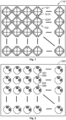
- Figure 1 shows a planar structure 110 with antenna bodies according to one embodiment of the invention.
- the antenna bodies are arranged in an array on a top side of a circuit board that is included in the planar structure 110. This means that the antenna bodies are organized in a pattern of straight rows and columns.
- the exact number of antenna bodies is not critical. However, of course, a larger number of antenna bodies is associated with higher efficiency than a ditto lower number.
- the pattern is equilateral, i.e. the number of rows equals the number of columns, say 2 by 2 to 40 by 40, preferably 6 by 6 to 25 by 25.
- first and second exemplifying antenna bodies are designated by reference numerals 121 and 122 respectively.
- the planar structure 110 further contains a ground-plane layer that is arranged below a bottom side of the circuit board, i.e. opposite to antenna bodies 121 and 122.
- Figure 2 shows an example of such a ground-plane layer 220 seen from a top side thereof.
- the ground-plane layer 220 is made of an electrically conductive material, such as a metal, e.g. aluminum.
- Each of the antenna bodies 121 and 122 contains a dome shaped structure, which is attached to the top side of the circuit board 210, for example by means of soldering and/or mechanical fasteners.
- the antenna bodies 121 and 122 are attached along a respective base of the dome shaped structure.
- the mechanical fasteners may be represented by snap in fasteners or an arrangement of compressed springs configured to provide galvanic contact between the antenna bodies 121 and 122 and a circuit pattern on the top side of the circuit board.
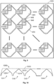
- FIG. 3 we see a cross-section side view, illustrating the structure of the antenna array according to one embodiment of the invention.
- Each antenna body 121 and 122 is connected to a respective top transmission line 350, which is configured to convey microwave signals to and/or from the antenna body 121 or 122 respectively, i.e. for transmitting and/or receiving electromagnetic energy.
- the top transmission lines 350 are implemented in suspended stripline design.
- the top transmission lines 350 are further connected to bottom transmission lines 330 via a respective coaxial probe 340 through the circuit board 210 and the ground-plane layer 220.
- the ground-plane layer 220 may be a solid piece of metal in which a pattern of cavities and openings have been milled out.
- the bottom transmission line 330 is implemented in suspended stripline design.
- a number of alternative bottom transmission line designs are also conceivable according to the invention. In fact, the same is true for the top transmission line design.
- any combination of top and bottom transmission line design is possible. The choice of the designs used is merely a matter of what is most suitable for the specific implementation.
- a plurality of vias 370 through the circuit board 210 connect the ground-plane layer 220 to circuitry on the top side of the circuit board 210 so that the ground plane effectively extends above the circuit board 210 and thus can be further connected to the antenna bodies 121 and 122.
- a resonance cavity 360 is arranged below the bottom side of the circuit board 210 between each of said antenna bodies 121 and 122 respectively.
- the resonance cavity 360 constitutes a stub, i.e. a length of waveguide connected at one end only, which is configured to direct as much as possible of the electromagnetic energy from the top transmission line 350 "upwards" towards the antenna bodies 121 and 122.
- the resonance cavity 360 configured to direct as much as possible of the electromagnetic energy that reaches the antenna bodies 121 and 122 "downwards" towards the top transmission line 350.
- the resonance cavity is represented by the reference numeral 260.
- the resonance cavity 260 is, in fact, a continuous milled-out volume between all the antenna elements, which each is mounted on a respective "island" 221 and 222 respectively where no, or only relatively little, material has been milled out from the solid piece of metal.
- each antenna body 121 and 122 contains electrically conductive surface elements.
- a first electrically conductive surface element 121H of a first antenna body 121 is configured to constitute a first portion of an antenna horn.
- a second electrically conductive surface element 122H of a second antenna body 122 is configured to constitute a second portion of the antenna horn.
- the first and second antenna bodies 121 and 122 adjoin one another in such a manner that the first and second electrically conductive surface elements 121H and 122H respectively are located closer to one another than any other surface elements of the first and second antenna bodies 121 and 122.
- the first and second electrically conductive surface elements 121H and 122H form a horn configured to convey electromagnetic waves towards or from the top transmission line 350 depending on whether the antenna receives or transmits signals.
- Each of the horns formed by the first and second electrically conductive surface elements 121H and 122H has a tapered profile towards the top side of the circuit board 210, for example as illustrated in Figure 3 .
- An aperture towards the resonance cavity 360 between the first and second electrically conductive surface elements 121H and 122H is symmetric around a normal to the top side of the circuit board 210.
- the distance between the first and second electrically conductive surface elements 121H and 122H along the circuit board 210, the center distance between the first and second antenna bodies 121 and 122, the height of the first and second antenna bodies 121 and 122 above the circuit board 210 and the profile of the first and second electrically conductive surface elements 121H and 122H are different design parameters, which are selected depending on the frequency spectrum, the efficiency required and various physical constraints placed on the implementation.
- each antenna body 121 and 122 is mirror symmetric in exactly two planes that are orthogonal to one another.
- the base of the dome shaped structure of the antenna bodies 121 and 122 may be octagon shaped, as shown in Figure 1 .
- the antenna bodies 121 and 122 are further preferably arranged in the array according to a pattern in which the first and second electrically conductive surface elements 121H and 122H of adjoining antenna bodies pairwise form a respective antenna horn in such a manner that the antenna array contains horns of first and second subsets.
- the horns of the first subset are configured to transmit and/or receive signals of a first polarization direction
- the horns of the second subset are configured to transmit and/or receive signals of a second polarization direction, which is orthogonal to the first polarization direction.
- each of the antenna bodies 121 and 122 form part of at least one horn that is included in the first subset and at least one horn that is included in the second subset.
- the first subset horns may contain all the electrically conductive surface elements 121H and 122H extending along a vertical direction
- the second subset horns may contain all the electrically conductive surface elements extending along a horizontal direction in the array of antenna bodies.
- each antenna body 121 and 122 is octagon shaped is advantageous because such geometry provides high isolation between signals representing the two orthogonal polarization directions.
- the octagon shape renders it straightforward to configure the antenna bodies so that their tapered profile and the distances between the antenna bodies is optimized to match a particular range of the electromagnetic spectrum in which the antenna array is to operate.
- the octagon-shaped base makes it possible to vary a distance along which an opening between the first and second electrically conductive surface elements 121H and 122H are effectively parallel to one another towards the resonance cavity 360 without the need to alter a center-to-center distance between the antenna bodies. From a design point-of-view, this is very beneficial when optimizing the design to a match particular frequency range of operation.
- Figure 4 shows a cross-section a side view illustrating the structure of the antenna array according to another embodiment of the invention.
- the top transmission line arrangement is implemented in a microstrip design 450
- the bottom transmission line is implemented by means of a coaxial cable 430.
- the planar structure 110 contains a circuit board 210 and a ground-plane layer 420, and the array of antenna bodies 121 and 122 being arranged on a top side of the circuit board 210, and each antenna body 121 and 122 contains a dome shaped structure being attached to the top side of the circuit board 210 along its base.
- Each antenna body 121 and 122 is connected to a respective top transmission line 450 configured to convey microwave signals to and/or from the antenna bodies 121 and 122.
- the top transmission lines 450 are connected to the bottom transmission lines 430 via coaxial probes 440 through the ground-plane layer 420.
- a resonance cavity 460 is arranged below a bottom side of the circuit board 210 between each of the antenna bodies 121 and 122.
- the top transmission line 450 together with a slotline in between the antenna bodies 121 and 122 and the resonance cavity 460 constitutes a so-called balun, i.e. a balanced transmission line to an unbalanced transmission line conversion.
- the balun is configured to convert the signal from being a balanced signal along the top transmission line 450 to an unbalanced signal between the antenna bodies 121 and 122 and the resonance cavity 460.
- a first circuit pattern 425 on the bottom side of the circuit board is electrically connected to the ground-plane layer 420.
- the first circuit pattern 425 is electrically connected to a second circuit pattern on the top side of the circuit board 210 by means of a plurality of vias 370 through the circuit board 210. Consequently, the ground plane also extends above the circuit board 210.
- Figure 9 shows the bottom side of the circuit board 910 and the first circuit pattern 425 according to this embodiment of the invention.
- the reference numeral 970 designates the positions of said plurality of vias through the circuit board 910.
- the reference numeral 940 designates a portion of the first circuit pattern being connected to the coaxial probe 440 through the ground-plane layer 420.
- FIG. 5 illustrates, by means of cross-section a side view, the structure of the antenna array according to another embodiment of the invention.
- the top transmission line arrangement is implemented in a stripline design 550
- the bottom transmission line is implemented by means of a suspended stripline 530.
- the planar structure 110 contains a circuit board 210 and a ground-plane layer 520, and the array of antenna bodies 121 and 122 being arranged on a top side of the circuit board 210, and each antenna body 121 and 122 contains a dome shaped structure being attached to the top side of the circuit board 210 along its base.
- Each antenna body 121 and 122 is connected to a respective top transmission line 550 configured to convey microwave signals to and/or from the antenna bodies 121 and 122, and the top transmission lines 550 are further connected to the bottom transmission lines 530 via coaxial probes 540 through the ground-plane layer 520.
- a resonance cavity 560 is arranged below a bottom side of the circuit board 210 between each of the antenna bodies 121 and 122.
- the ground-plane layer 520 is electrically connected to a first circuit pattern on the bottom side of the circuit board 210, which first circuit pattern is further electrically connected to a second circuit pattern on the top side of the circuit board 210 by means of a plurality of vias 570 through the circuit board 210 so as to extend a ground plane represented by the ground-plane layer 520 to the top side of the circuit board 210.
- FIG. 6 illustrates, by means of cross-section a side view, the structure of the antenna array according to another embodiment of the invention.
- the top transmission line arrangement is implemented in a suspended stripline design 650
- the bottom transmission line is implemented by means of a coaxial cable 630.
- the planar structure 110 contains a circuit board 210 and a ground-plane layer 620, and the array of antenna bodies 121 and 122 being arranged on a top side of the circuit board 210, and each antenna body 121 and 122 contains a dome shaped structure being attached to the top side of the circuit board 210 along its base.
- Each antenna body 121 and 122 is connected to a respective top transmission line 650 configured to convey microwave signals to and/or from the antenna bodies 121 and 122, and the top transmission lines 650 are further connected to the bottom transmission lines 630 via coaxial probes 640 through the ground-plane layer 620.
- a resonance cavity 660 is arranged below a bottom side of the circuit board 210 between each of the antenna bodies 121 and 122.
- the ground-plane layer 620 is electrically connected to a first circuit pattern on the bottom side of the circuit board 210, which first circuit pattern is further electrically connected to a second circuit pattern on the top side of the circuit board 210 by means of a plurality of vias 670 through the circuit board 210 so as to extend a ground plane represented by the ground-plane layer 620 to the top side of the circuit board 210.
- Figure 7 illustrates, by means of cross-section a side view, the structure of the antenna array according to another embodiment of the invention.
- the top transmission line arrangement is implemented in a stripline design 750
- the bottom transmission line 730 is likewise implemented by means of a stripline design.
- the planar structure 110 contains a circuit board 210 and a ground-plane layer 720, and the array of antenna bodies 121 and 122 being arranged on a top side of the circuit board 210, and each antenna body 121 and 122 contains a dome shaped structure being attached to the top side of the circuit board 210 along its base.
- Each antenna body 121 and 122 is connected to a respective top transmission line 750 configured to convey microwave signals to and/or from the antenna bodies 121 and 122, and the top transmission lines 750 are further connected to the bottom transmission lines 730 via coaxial probes 740 through the ground-plane layer 720.
- a resonance cavity 760 is arranged below a bottom side of the circuit board 210 between each of the antenna bodies 121 and 122.
- the ground-plane layer 720 is electrically connected to a first circuit pattern on the bottom side of the circuit board 210, which first circuit pattern is further electrically connected to a second circuit pattern on the top side of the circuit board 210 by means of a plurality of vias 770 through the circuit board 210 so as to extend a ground plane represented by the ground-plane layer 720 to the top side of the circuit board 210.
- Figure 8 illustrates, by means of cross-section a side view, the structure of the antenna array according to one embodiment of the invention.
- the top transmission line arrangement is implemented in a stripline design 850
- the bottom transmission line 830 is implemented by means of a microstrip design.
- the planar structure 110 contains a circuit board 210 and a ground-plane layer 820, and the array of antenna bodies 121 and 122 being arranged on a top side of the circuit board 210, and each antenna body 121 and 122 contains a dome shaped structure being attached to the top side of the circuit board 210 along its base.
- Each antenna body 121 and 122 is connected to a respective top transmission line 850 configured to convey microwave signals to and/or from the antenna bodies 121 and 122, and the top transmission lines 850 are further connected to the bottom transmission lines 830 via coaxial probes 840 through the ground-plane layer 820.
- a resonance cavity 860 is arranged below a bottom side of the circuit board 210 between each of the antenna bodies 121 and 122.
- the ground-plane layer 820 is electrically connected to a first circuit pattern on the bottom side of the circuit board 210, which first circuit pattern is further electrically connected to a second circuit pattern on the top side of the circuit board 210 by means of a plurality of vias 870 through the circuit board 210 so as to extend a ground plane represented by the ground-plane layer 820 to the top side of the circuit board 210.
- Figure 10 shows a cross-section side view of a shell member 1000 implementing the antenna bodies according to an embodiment of the invention that is combinable with any of the above-described embodiments.
- the shell member 1000 is made of a non-conductive material, and the shell member 1000 is arranged on the planar structure 110 instead of the antenna bodies 121 and 122.
- the shell member 1000 contains a plurality of cavities Cn1, Cn2, Cn3, ..., Cnm each of replaces one of the antenna bodies 121 and 122 by means of an electrically conductive layer 1015 that covers a respective active surface of each cavity of said plurality of cavities Cn1, Cn2, Cn3, ..., Cnm.
- the active surface faces the top side of the circuit board 210, thus representing a circuit element equivalent to the outer surface an antenna body 121 or 122.
- the shell member 1000 has a generally flat exterior surface 1010 facing away from the top side of the circuit board 210, since thereby the antenna obtains a nice-looking and easy to clean exterior surface.
Landscapes
- Waveguide Aerials (AREA)
- Variable-Direction Aerials And Aerial Arrays (AREA)
Claims (9)
- Antennenanordnung, umfassend eine Anordnung von Antennenkörpern (121, 122), die an einer planaren Struktur (110) angeordnet ist,wobei die planare Struktur (110) eine Leiterplatte (210) und eine Masseplattenschicht (220, 320, 420, 520, 620, 720, 820) umfasst,wobei die Anordnung von Antennenkörpern (121, 122) auf einer Oberseite der Leiterplatte (210) angeordnet ist,wobei jeder der Antennenkörper (121, 122) eine kuppelförmige Struktur aufweist, die an der Oberseite der Leiterplatte (210) entlang einer Basis der kuppelförmigen Struktur angebracht ist,wobei jeder der Antennenkörper (121, 122) mit einer jeweiligen oberen Übertragungsleitung (350, 450, 550, 650, 750, 850) verbunden ist, die dazu ausgelegt ist, Mikrowellensignale an die Antennenkörper (121, 122) oder von diesen zu übertragen,wobei die oberen Übertragungsleitungen (350, 450, 550, 650, 750, 850) ferner über Koaxialsonden (340, 440, 540, 640, 740, 840) durch die Masseplattenschicht (220, 320, 420, 520, 620, 720, 820) mit unteren Übertragungsleitungen (330, 430, 530, 630, 730) verbunden sind, undwobei ein Resonanzhohlraum (260, 360, 460, 560, 660, 760, 860) unterhalb einer Unterseite der Leiterplatte (210) zwischen jedem der Antennenkörper (121, 122) angeordnet ist,wobei die Antennenanordnung ferner ein Hüllenelement (1000) aus einem nicht leitenden Material umfasst, wobei das Hüllenelement (1000) auf der planaren Struktur (110) angeordnet ist und eine Vielzahl von Hohlräumen (Cn1, Cn2, Cn3, ..., Cnm) umfasst, von denen jeder mittels einer elektrisch leitenden Schicht (1015), die eine jeweilige aktive Fläche jedes Hohlraums der Vielzahl von Hohlräumen (Cn1, Cn2, Cn3, ..., Cnm) bedeckt, einen der Antennenkörper (121, 122) bildet, wobei die aktive Fläche der Oberseite der Leiterplatte (210) zugewandt ist.
- Antennenanordnung nach Anspruch 1, wobei:ein erstes elektrisch leitendes Flächenelement (121H) eines ersten Antennenkörpers (121) der Antennenkörper (121, 122) dazu ausgelegt ist, einen ersten Abschnitt eines Antennenhorns zu bilden, undein zweites elektrisch leitendes Flächenelement (122H) eines zweiten Antennenkörpers (122) der Antennenkörper (121, 122) dazu ausgelegt ist, einen zweiten Abschnitt des Antennenhorns zu bilden, wobei der erste und der zweite Antennenkörper (121, 122) derart aneinander angrenzen, dass das erste und das zweite elektrisch leitende Flächenelement (121H; 122H) näher beieinander angeordnet sind als beliebige andere Flächenelemente des ersten und des zweiten Antennenkörpers (121, 122).
- Antennenanordnung nach Anspruch 2, wobei:jeder der Antennenkörper (121, 122) in genau zwei Ebenen, die zueinander orthogonal sind, spiegelsymmetrisch ist,die Antennenkörper (121, 122) in der Anordnung gemäß einem Muster angeordnet sind, in dem das erste und das zweite elektrisch leitende Flächenelement angrenzender Antennenkörper paarweise derart ein jeweiliges Antennenhorn ausbilden, dass die Antennenanordnung Antennenelemente umfasst, die dazu ausgelegt sind, Signale einer ersten Polarisationsrichtung über eine erste Teilmenge der Hörner zu senden und/oder zu empfangen und Signale einer zweiten Polarisationsrichtung über eine zweite Teilmenge der Hörner zu senden und/oder zu empfangen, wobei die erste und die zweite Polarisationsrichtung orthogonal zueinander sind und jeder der Antennenkörper (121, 122) einen Teil von mindestens einem Horn, das in der ersten Teilmenge beinhaltet ist, und mindestens einem Horn, das in der zweiten Teilmenge beinhaltet ist, ausbildet.
- Antennenanordnung nach Anspruch 3, wobei:die Basis der kuppelförmigen Struktur jedes der Antennenkörper (121, 122) achteckig geformt ist, undjedes der Hörner, die durch das erste und das zweite elektrisch leitende Flächenelement (121H; 122H) ausgebildet sind, ein sich zur Oberseite der Leiterplatte (210) hin verjüngendes Profil aufweist, und eine Öffnung zwischen dem ersten und dem zweiten elektrisch leitenden Flächenelement (121H; 122H) um eine Normale zur Oberseite der Leiterplatte (210) symmetrisch ist.
- Antennenanordnung nach einem der vorhergehenden Ansprüche, wobei:
die Masseplattenschicht (420) elektrisch mit einem ersten Schaltungsmuster (425) auf der Unterseite der Leiterplatte (210) verbunden ist, wobei das erste Schaltungsmuster (425) ferner elektrisch mit einem zweiten Schaltungsmuster auf der Oberseite der Leiterplatte (210) mittels einer Vielzahl von Durchkontaktierungen (370, 470, 570, 670, 770, 870, 970) durch die Leiterplatte (210) verbunden ist, um eine durch die Masseplattenschicht (420) dargestellte Masseplatte bis zur Oberseite der Leiterplatte (210) zu verlängern. - Antennenanordnung gemäß einem der vorhergehenden Ansprüche, wobei:die obere Übertragungsleitungsanordnung als Brennerleitungsausgestaltung (350) umgesetzt ist unddie untere Übertragungsleitung mittels einem von einer Brennerleitungsausgestaltung (330), einem Koaxialkabel (430, 630), einer Streifenleitungsausgestaltung (730) und einer Mikrostreifenleitungsausgestaltung (830) umgesetzt ist.
- Antennenanordnung nach einem der Ansprüche 1 bis 5, wobei:die obere Übertragungsleitungsanordnung in einer Mikrostreifenleitungsausgestaltung (450) umgesetzt ist, unddie untere Übertragungsleitung mittels einem von einer Brennerleitungsausgestaltung (330), einem Koaxialkabel (430, 630), einer Streifenleitungsausgestaltung (730) und einer Mikrostreifenleitungsausgestaltung (830) umgesetzt ist.
- Antennenanordnung nach einem der Ansprüche 1 bis 5, wobei:die obere Übertragungsleitungsanordnung als Streifenleitungsausgestaltung (550) umgesetzt ist unddie untere Übertragungsleitung mittels einem von einer Brennerleitungsausgestaltung (330), einem Koaxialkabel (430, 630), einer Streifenleitungsausgestaltung (730) und einer Mikrostreifenleitungsausgestaltung (830) umgesetzt ist.
- Antennenanordnung gemäß Anspruch 1, wobei das Hüllenelement (1000) eine im Allgemeinen flache Außenfläche (1010) aufweist, die von der Oberseite der Leiterplatte (210) abgewandt ist.
Priority Applications (2)
| Application Number | Priority Date | Filing Date | Title |
|---|---|---|---|
| EP22173759.6A EP4064456B1 (de) | 2019-06-05 | 2019-06-05 | Antennenanordnung |
| ES22173759T ES2986810T3 (es) | 2019-06-05 | 2019-06-05 | Sistema de antenas |
Applications Claiming Priority (3)
| Application Number | Priority Date | Filing Date | Title |
|---|---|---|---|
| EP22173759.6A EP4064456B1 (de) | 2019-06-05 | 2019-06-05 | Antennenanordnung |
| EP19729499.4A EP3981045B1 (de) | 2019-06-05 | 2019-06-05 | Gruppenantenne |
| PCT/EP2019/064618 WO2020244750A1 (en) | 2019-06-05 | 2019-06-05 | Antenna array |
Related Parent Applications (2)
| Application Number | Title | Priority Date | Filing Date |
|---|---|---|---|
| EP19729499.4A Division-Into EP3981045B1 (de) | 2019-06-05 | 2019-06-05 | Gruppenantenne |
| EP19729499.4A Division EP3981045B1 (de) | 2019-06-05 | 2019-06-05 | Gruppenantenne |
Publications (3)
| Publication Number | Publication Date |
|---|---|
| EP4064456A1 EP4064456A1 (de) | 2022-09-28 |
| EP4064456B1 true EP4064456B1 (de) | 2024-07-24 |
| EP4064456C0 EP4064456C0 (de) | 2024-07-24 |
Family
ID=66810793
Family Applications (2)
| Application Number | Title | Priority Date | Filing Date |
|---|---|---|---|
| EP19729499.4A Active EP3981045B1 (de) | 2019-06-05 | 2019-06-05 | Gruppenantenne |
| EP22173759.6A Active EP4064456B1 (de) | 2019-06-05 | 2019-06-05 | Antennenanordnung |
Family Applications Before (1)
| Application Number | Title | Priority Date | Filing Date |
|---|---|---|---|
| EP19729499.4A Active EP3981045B1 (de) | 2019-06-05 | 2019-06-05 | Gruppenantenne |
Country Status (4)
| Country | Link |
|---|---|
| US (1) | US12155119B2 (de) |
| EP (2) | EP3981045B1 (de) |
| ES (2) | ES3027978T3 (de) |
| WO (1) | WO2020244750A1 (de) |
Families Citing this family (2)
| Publication number | Priority date | Publication date | Assignee | Title |
|---|---|---|---|---|
| WO2021101425A1 (en) * | 2019-11-22 | 2021-05-27 | Saab Ab | A feeding system for an array of bor antenna elements |
| EP4062492A4 (de) * | 2019-11-22 | 2023-07-26 | Saab Ab | Invertierte antennenelemente |
Family Cites Families (41)
| Publication number | Priority date | Publication date | Assignee | Title |
|---|---|---|---|---|
| US4345256A (en) | 1980-12-15 | 1982-08-17 | Sperry Corporation | Steerable directional antenna |
| JPH06101646B2 (ja) | 1985-10-09 | 1994-12-12 | 富士通株式会社 | 無線通信装置 |
| US5398035A (en) | 1992-11-30 | 1995-03-14 | The United States Of America As Represented By The Administrator Of The National Aeronautics And Space Administration | Satellite-tracking millimeter-wave reflector antenna system for mobile satellite-tracking |
| US5517205A (en) | 1993-03-31 | 1996-05-14 | Kvh Industries, Inc. | Two axis mount pointing apparatus |
| JP2692666B2 (ja) | 1995-11-30 | 1997-12-17 | 日本電気株式会社 | 衛星放送受信用コンバータ |
| JPH10178313A (ja) | 1996-12-19 | 1998-06-30 | Mitsubishi Electric Corp | アンテナ装置 |
| US6538612B1 (en) | 1997-03-11 | 2003-03-25 | Lael D. King | Satellite locator system |
| JP3619060B2 (ja) | 1999-06-25 | 2005-02-09 | 三菱電機株式会社 | 多周波数帯共用アンテナ装置 |
| US6452540B1 (en) | 2001-01-12 | 2002-09-17 | Trw Inc. | Method and apparatus for controlling spot beam configurations for a communications satellite |
| US6653981B2 (en) | 2001-11-01 | 2003-11-25 | Tia Mobile, Inc. | Easy set-up, low profile, vehicle mounted, satellite antenna |
| SE0202123L (sv) * | 2002-07-08 | 2004-01-07 | Saab Ab | Elektriskt styrd bredbandig gruppantenn, antennelement lämpat att ingå i en sådan gruppantenn, samt antennmodul innefattande ett flertal sådana antennelement |
| US7705793B2 (en) | 2004-06-10 | 2010-04-27 | Raysat Antenna Systems | Applications for low profile two way satellite antenna system |
| US7542716B2 (en) | 2003-01-28 | 2009-06-02 | The Boeing Company | Systems and methods for digital processing of satellite communications data |
| US7911400B2 (en) | 2004-01-07 | 2011-03-22 | Raysat Antenna Systems, L.L.C. | Applications for low profile two-way satellite antenna system |
| US6999036B2 (en) | 2004-01-07 | 2006-02-14 | Raysat Cyprus Limited | Mobile antenna system for satellite communications |
| US7432868B2 (en) | 2004-04-26 | 2008-10-07 | Spencer Webb | Portable antenna positioner apparatus and method |
| US8786506B2 (en) | 2004-04-26 | 2014-07-22 | Antennasys, Inc. | Compact portable antenna positioner system and method |
| US7173571B2 (en) | 2004-04-26 | 2007-02-06 | Windmill International, Inc. | Portable antenna positioner apparatus and method |
| US7420522B1 (en) * | 2004-09-29 | 2008-09-02 | The United States Of America As Represented By The Secretary Of The Navy | Electromagnetic radiation interface system and method |
| DE602005008965D1 (de) | 2005-09-17 | 2008-09-25 | Deutsch Zentr Luft & Raumfahrt | Aeronautisches Kommunikationssystem |
| WO2007064094A1 (en) | 2005-12-01 | 2007-06-07 | Electronics And Telecommunications Research Institute | Low profile mobile tri-band antenna system |
| KR20070060630A (ko) | 2005-12-09 | 2007-06-13 | 한국전자통신연구원 | 위성추적 안테나 시스템 |
| US20070135040A1 (en) | 2005-12-12 | 2007-06-14 | Draim John E | Methods for effecting seamless handover and enhancing capacity in elliptical orbit satellite communications systems |
| US8350767B2 (en) | 2007-05-30 | 2013-01-08 | Massachusetts Institute Of Technology | Notch antenna having a low profile stripline feed |
| WO2009039998A2 (en) | 2007-09-13 | 2009-04-02 | Overhorizon (Cyprus) Plc | Antenna system for communications on-the-move |
| WO2010098623A2 (ko) | 2009-02-26 | 2010-09-02 | 엘지전자 주식회사 | 광대역 무선 접속 시스템에서 핸드오버 수행 중 시스템 정보 갱신 방법 |
| US20110105126A1 (en) | 2009-06-15 | 2011-05-05 | The Aerospace Corportion | Terminal initiated intrasatellite antenna handover method |
| FR2950762B1 (fr) | 2009-09-28 | 2011-10-21 | Astrium Sas | Systeme de telecommunications par satellite multifaisceaux et procede de formation de faisceaux |
| US8482477B2 (en) | 2010-03-09 | 2013-07-09 | Raytheon Company | Foam layer transmission line structures |
| US9425888B2 (en) | 2012-08-08 | 2016-08-23 | Asia Satellite Telecommunications Company Limited | Methods and systems for providing high-speed connectivity to aircraft |
| US9952388B2 (en) * | 2012-09-16 | 2018-04-24 | Shalom Wertsberger | Nano-scale continuous resonance trap refractor based splitter, combiner, and reflector |
| IL235416B (en) | 2014-10-30 | 2019-02-28 | Gilat Telecom Ltd | Satellite communication in a closed place |
| EP3235059B1 (de) | 2014-12-19 | 2020-02-05 | Saab AB | Oberflächenmontiertes breitbandelement |
| WO2016141177A1 (en) * | 2015-03-03 | 2016-09-09 | Massachusetts, University Of | Low cross-polarization decade-bandwidth ultra-wideband antenna element and array |
| US9979082B2 (en) | 2015-08-10 | 2018-05-22 | Viasat, Inc. | Method and apparatus for beam-steerable antenna with single-drive mechanism |
| US9673888B2 (en) | 2015-09-23 | 2017-06-06 | Qualcomm Incorporated | Acquiring LEO satellites without compass |
| US10715302B2 (en) | 2015-10-14 | 2020-07-14 | Wilson Electronics, Llc | Channelization for signal boosters |
| US10651925B2 (en) | 2016-04-21 | 2020-05-12 | University Of Louisiana At Lafayette | Experimental smartphone ground station grid system |
| WO2018022308A2 (en) * | 2016-07-14 | 2018-02-01 | Massachusetts Institute Of Technology | Foam radiator |
| US10826186B2 (en) * | 2017-08-28 | 2020-11-03 | Raytheon Company | Surface mounted notch radiator with folded balun |
| US10777907B2 (en) * | 2018-08-22 | 2020-09-15 | The Boeing Company | Antenna horn, antenna, and antenna array for a radiating printed circuit board, and methods therefor |
-
2019
- 2019-06-05 EP EP19729499.4A patent/EP3981045B1/de active Active
- 2019-06-05 US US17/616,294 patent/US12155119B2/en active Active
- 2019-06-05 EP EP22173759.6A patent/EP4064456B1/de active Active
- 2019-06-05 ES ES19729499T patent/ES3027978T3/es active Active
- 2019-06-05 ES ES22173759T patent/ES2986810T3/es active Active
- 2019-06-05 WO PCT/EP2019/064618 patent/WO2020244750A1/en not_active Ceased
Also Published As
| Publication number | Publication date |
|---|---|
| WO2020244750A1 (en) | 2020-12-10 |
| EP3981045B1 (de) | 2025-05-07 |
| US20220158340A1 (en) | 2022-05-19 |
| ES3027978T3 (en) | 2025-06-17 |
| EP3981045C0 (de) | 2025-05-07 |
| EP4064456C0 (de) | 2024-07-24 |
| EP3981045A1 (de) | 2022-04-13 |
| US12155119B2 (en) | 2024-11-26 |
| EP4064456A1 (de) | 2022-09-28 |
| ES2986810T3 (es) | 2024-11-12 |
Similar Documents
| Publication | Publication Date | Title |
|---|---|---|
| US8749446B2 (en) | Wide-band linked-ring antenna element for phased arrays | |
| US5650788A (en) | Terrestrial antennas for satellite communication system | |
| JP6938655B2 (ja) | ボウタイアンテナ装置 | |
| US9306262B2 (en) | Stacked bowtie radiator with integrated balun | |
| US6483464B2 (en) | Patch dipole array antenna including a feed line organizer body and related methods | |
| EP2015396A2 (de) | Zirkular polarisierte Gruppenantenne | |
| US20220239007A1 (en) | Luneburg lens-based satellite antenna system | |
| US20210159597A1 (en) | High-gain, wide-angle, multi-beam, multi-frequency beamforming lens antenna | |
| WO2003098743A1 (en) | Wideband antenna array | |
| EP1849211B1 (de) | Array-antenne mit monolithischer antennenzuführanordnung und entsprechendes verfahren | |
| JP2004513549A (ja) | パッチダイポールのアレイアンテナ及び関連の方法 | |
| US9300054B2 (en) | Printed circuit board based feed horn | |
| US11710902B2 (en) | Dual-polarized magneto-electric antenna array | |
| EP4064456B1 (de) | Antennenanordnung | |
| US10950952B1 (en) | Spherical space feed for antenna array systems and methods | |
| EP3028341B1 (de) | Gestapelter bowtie-heizkörper mit integriertem balun | |
| US12021305B1 (en) | Conformal antenna system | |
| US11482794B1 (en) | Slot-fed unit cell and current sheet array | |
| Wu et al. | A beam-switching planar antenna module with 360° in-plane coverage for drone collision avoidance radar | |
| SE1950669A1 (en) | Antenna array | |
| GB2411524A (en) | Dual slot cavity antenna with slots of differing resonant frequencies | |
| EP1564843A1 (de) | Zirkular polarisierte Gruppenantenne | |
| AU2002312556A1 (en) | Patchdipole array antenna including a feed line organizer body and related methods |
Legal Events
| Date | Code | Title | Description |
|---|---|---|---|
| PUAI | Public reference made under article 153(3) epc to a published international application that has entered the european phase |
Free format text: ORIGINAL CODE: 0009012 |
|
| STAA | Information on the status of an ep patent application or granted ep patent |
Free format text: STATUS: THE APPLICATION HAS BEEN PUBLISHED |
|
| AC | Divisional application: reference to earlier application |
Ref document number: 3981045 Country of ref document: EP Kind code of ref document: P |
|
| AK | Designated contracting states |
Kind code of ref document: A1 Designated state(s): AL AT BE BG CH CY CZ DE DK EE ES FI FR GB GR HR HU IE IS IT LI LT LU LV MC MK MT NL NO PL PT RO RS SE SI SK SM TR |
|
| STAA | Information on the status of an ep patent application or granted ep patent |
Free format text: STATUS: REQUEST FOR EXAMINATION WAS MADE |
|
| 17P | Request for examination filed |
Effective date: 20221004 |
|
| RBV | Designated contracting states (corrected) |
Designated state(s): AL AT BE BG CH CY CZ DE DK EE ES FI FR GB GR HR HU IE IS IT LI LT LU LV MC MK MT NL NO PL PT RO RS SE SI SK SM TR |
|
| P01 | Opt-out of the competence of the unified patent court (upc) registered |
Effective date: 20230517 |
|
| GRAP | Despatch of communication of intention to grant a patent |
Free format text: ORIGINAL CODE: EPIDOSNIGR1 |
|
| STAA | Information on the status of an ep patent application or granted ep patent |
Free format text: STATUS: GRANT OF PATENT IS INTENDED |
|
| INTG | Intention to grant announced |
Effective date: 20240206 |
|
| GRAS | Grant fee paid |
Free format text: ORIGINAL CODE: EPIDOSNIGR3 |
|
| GRAA | (expected) grant |
Free format text: ORIGINAL CODE: 0009210 |
|
| STAA | Information on the status of an ep patent application or granted ep patent |
Free format text: STATUS: THE PATENT HAS BEEN GRANTED |
|
| AC | Divisional application: reference to earlier application |
Ref document number: 3981045 Country of ref document: EP Kind code of ref document: P |
|
| AK | Designated contracting states |
Kind code of ref document: B1 Designated state(s): AL AT BE BG CH CY CZ DE DK EE ES FI FR GB GR HR HU IE IS IT LI LT LU LV MC MK MT NL NO PL PT RO RS SE SI SK SM TR |
|
| REG | Reference to a national code |
Ref country code: GB Ref legal event code: FG4D |
|
| REG | Reference to a national code |
Ref country code: CH Ref legal event code: EP |
|
| REG | Reference to a national code |
Ref country code: DE Ref legal event code: R096 Ref document number: 602019055963 Country of ref document: DE |
|
| REG | Reference to a national code |
Ref country code: IE Ref legal event code: FG4D |
|
| U01 | Request for unitary effect filed |
Effective date: 20240724 |
|
| P04 | Withdrawal of opt-out of the competence of the unified patent court (upc) registered |
Free format text: CASE NUMBER: APP_44106/2024 Effective date: 20240729 |
|
| U07 | Unitary effect registered |
Designated state(s): AT BE BG DE DK EE FI FR IT LT LU LV MT NL PT SE SI Effective date: 20240731 |
|
| REG | Reference to a national code |
Ref country code: ES Ref legal event code: FG2A Ref document number: 2986810 Country of ref document: ES Kind code of ref document: T3 Effective date: 20241112 |
|
| P05 | Withdrawal of opt-out of the competence of the unified patent court (upc) changed |
Free format text: CASE NUMBER: APP_44106/2024 Effective date: 20240731 |
|
| PG25 | Lapsed in a contracting state [announced via postgrant information from national office to epo] |
Ref country code: NO Free format text: LAPSE BECAUSE OF FAILURE TO SUBMIT A TRANSLATION OF THE DESCRIPTION OR TO PAY THE FEE WITHIN THE PRESCRIBED TIME-LIMIT Effective date: 20241024 |
|
| PG25 | Lapsed in a contracting state [announced via postgrant information from national office to epo] |
Ref country code: PL Free format text: LAPSE BECAUSE OF FAILURE TO SUBMIT A TRANSLATION OF THE DESCRIPTION OR TO PAY THE FEE WITHIN THE PRESCRIBED TIME-LIMIT Effective date: 20240724 Ref country code: GR Free format text: LAPSE BECAUSE OF FAILURE TO SUBMIT A TRANSLATION OF THE DESCRIPTION OR TO PAY THE FEE WITHIN THE PRESCRIBED TIME-LIMIT Effective date: 20241025 |
|
| PG25 | Lapsed in a contracting state [announced via postgrant information from national office to epo] |
Ref country code: IS Free format text: LAPSE BECAUSE OF FAILURE TO SUBMIT A TRANSLATION OF THE DESCRIPTION OR TO PAY THE FEE WITHIN THE PRESCRIBED TIME-LIMIT Effective date: 20241124 |
|
| PG25 | Lapsed in a contracting state [announced via postgrant information from national office to epo] |
Ref country code: HR Free format text: LAPSE BECAUSE OF FAILURE TO SUBMIT A TRANSLATION OF THE DESCRIPTION OR TO PAY THE FEE WITHIN THE PRESCRIBED TIME-LIMIT Effective date: 20240724 |
|
| PG25 | Lapsed in a contracting state [announced via postgrant information from national office to epo] |
Ref country code: RS Free format text: LAPSE BECAUSE OF FAILURE TO SUBMIT A TRANSLATION OF THE DESCRIPTION OR TO PAY THE FEE WITHIN THE PRESCRIBED TIME-LIMIT Effective date: 20241024 |
|
| PG25 | Lapsed in a contracting state [announced via postgrant information from national office to epo] |
Ref country code: RS Free format text: LAPSE BECAUSE OF FAILURE TO SUBMIT A TRANSLATION OF THE DESCRIPTION OR TO PAY THE FEE WITHIN THE PRESCRIBED TIME-LIMIT Effective date: 20241024 Ref country code: PL Free format text: LAPSE BECAUSE OF FAILURE TO SUBMIT A TRANSLATION OF THE DESCRIPTION OR TO PAY THE FEE WITHIN THE PRESCRIBED TIME-LIMIT Effective date: 20240724 Ref country code: NO Free format text: LAPSE BECAUSE OF FAILURE TO SUBMIT A TRANSLATION OF THE DESCRIPTION OR TO PAY THE FEE WITHIN THE PRESCRIBED TIME-LIMIT Effective date: 20241024 Ref country code: IS Free format text: LAPSE BECAUSE OF FAILURE TO SUBMIT A TRANSLATION OF THE DESCRIPTION OR TO PAY THE FEE WITHIN THE PRESCRIBED TIME-LIMIT Effective date: 20241124 Ref country code: HR Free format text: LAPSE BECAUSE OF FAILURE TO SUBMIT A TRANSLATION OF THE DESCRIPTION OR TO PAY THE FEE WITHIN THE PRESCRIBED TIME-LIMIT Effective date: 20240724 Ref country code: GR Free format text: LAPSE BECAUSE OF FAILURE TO SUBMIT A TRANSLATION OF THE DESCRIPTION OR TO PAY THE FEE WITHIN THE PRESCRIBED TIME-LIMIT Effective date: 20241025 |
|
| PG25 | Lapsed in a contracting state [announced via postgrant information from national office to epo] |
Ref country code: RO Free format text: LAPSE BECAUSE OF FAILURE TO SUBMIT A TRANSLATION OF THE DESCRIPTION OR TO PAY THE FEE WITHIN THE PRESCRIBED TIME-LIMIT Effective date: 20240724 Ref country code: SM Free format text: LAPSE BECAUSE OF FAILURE TO SUBMIT A TRANSLATION OF THE DESCRIPTION OR TO PAY THE FEE WITHIN THE PRESCRIBED TIME-LIMIT Effective date: 20240724 |
|
| PG25 | Lapsed in a contracting state [announced via postgrant information from national office to epo] |
Ref country code: CZ Free format text: LAPSE BECAUSE OF FAILURE TO SUBMIT A TRANSLATION OF THE DESCRIPTION OR TO PAY THE FEE WITHIN THE PRESCRIBED TIME-LIMIT Effective date: 20240724 |
|
| PG25 | Lapsed in a contracting state [announced via postgrant information from national office to epo] |
Ref country code: SK Free format text: LAPSE BECAUSE OF FAILURE TO SUBMIT A TRANSLATION OF THE DESCRIPTION OR TO PAY THE FEE WITHIN THE PRESCRIBED TIME-LIMIT Effective date: 20240724 |
|
| PLBE | No opposition filed within time limit |
Free format text: ORIGINAL CODE: 0009261 |
|
| STAA | Information on the status of an ep patent application or granted ep patent |
Free format text: STATUS: NO OPPOSITION FILED WITHIN TIME LIMIT |
|
| 26N | No opposition filed |
Effective date: 20250425 |
|
| PGFP | Annual fee paid to national office [announced via postgrant information from national office to epo] |
Ref country code: GB Payment date: 20250618 Year of fee payment: 7 |
|
| U20 | Renewal fee for the european patent with unitary effect paid |
Year of fee payment: 7 Effective date: 20250617 |
|
| PGFP | Annual fee paid to national office [announced via postgrant information from national office to epo] |
Ref country code: ES Payment date: 20250710 Year of fee payment: 7 |