EP4064375A1 - Material mit negativer spin-polarisation und negativer anisotropie - Google Patents
Material mit negativer spin-polarisation und negativer anisotropie Download PDFInfo
- Publication number
- EP4064375A1 EP4064375A1 EP21178307.1A EP21178307A EP4064375A1 EP 4064375 A1 EP4064375 A1 EP 4064375A1 EP 21178307 A EP21178307 A EP 21178307A EP 4064375 A1 EP4064375 A1 EP 4064375A1
- Authority
- EP
- European Patent Office
- Prior art keywords
- sublayer
- multilayer structure
- fecr
- spintronic device
- layer
- Prior art date
- Legal status (The legal status is an assumption and is not a legal conclusion. Google has not performed a legal analysis and makes no representation as to the accuracy of the status listed.)
- Granted
Links
Images




Classifications
-
- G—PHYSICS
- G11—INFORMATION STORAGE
- G11B—INFORMATION STORAGE BASED ON RELATIVE MOVEMENT BETWEEN RECORD CARRIER AND TRANSDUCER
- G11B5/00—Recording by magnetisation or demagnetisation of a record carrier; Reproducing by magnetic means; Record carriers therefor
- G11B5/127—Structure or manufacture of heads, e.g. inductive
- G11B5/33—Structure or manufacture of flux-sensitive heads, i.e. for reproduction only; Combination of such heads with means for recording or erasing only
- G11B5/39—Structure or manufacture of flux-sensitive heads, i.e. for reproduction only; Combination of such heads with means for recording or erasing only using magneto-resistive devices or effects
- G11B5/3903—Structure or manufacture of flux-sensitive heads, i.e. for reproduction only; Combination of such heads with means for recording or erasing only using magneto-resistive devices or effects using magnetic thin film layers or their effects, the films being part of integrated structures
- G11B5/3906—Details related to the use of magnetic thin film layers or to their effects
- G11B5/3909—Arrangements using a magnetic tunnel junction
-
- H—ELECTRICITY
- H10—SEMICONDUCTOR DEVICES; ELECTRIC SOLID-STATE DEVICES NOT OTHERWISE PROVIDED FOR
- H10N—ELECTRIC SOLID-STATE DEVICES NOT OTHERWISE PROVIDED FOR
- H10N50/00—Galvanomagnetic devices
- H10N50/80—Constructional details
-
- C—CHEMISTRY; METALLURGY
- C22—METALLURGY; FERROUS OR NON-FERROUS ALLOYS; TREATMENT OF ALLOYS OR NON-FERROUS METALS
- C22C—ALLOYS
- C22C19/00—Alloys based on nickel or cobalt
- C22C19/07—Alloys based on nickel or cobalt based on cobalt
-
- C—CHEMISTRY; METALLURGY
- C22—METALLURGY; FERROUS OR NON-FERROUS ALLOYS; TREATMENT OF ALLOYS OR NON-FERROUS METALS
- C22C—ALLOYS
- C22C38/00—Ferrous alloys, e.g. steel alloys
- C22C38/08—Ferrous alloys, e.g. steel alloys containing nickel
-
- C—CHEMISTRY; METALLURGY
- C22—METALLURGY; FERROUS OR NON-FERROUS ALLOYS; TREATMENT OF ALLOYS OR NON-FERROUS METALS
- C22C—ALLOYS
- C22C38/00—Ferrous alloys, e.g. steel alloys
- C22C38/10—Ferrous alloys, e.g. steel alloys containing cobalt
-
- C—CHEMISTRY; METALLURGY
- C22—METALLURGY; FERROUS OR NON-FERROUS ALLOYS; TREATMENT OF ALLOYS OR NON-FERROUS METALS
- C22C—ALLOYS
- C22C38/00—Ferrous alloys, e.g. steel alloys
- C22C38/10—Ferrous alloys, e.g. steel alloys containing cobalt
- C22C38/105—Ferrous alloys, e.g. steel alloys containing cobalt containing Co and Ni
-
- C—CHEMISTRY; METALLURGY
- C22—METALLURGY; FERROUS OR NON-FERROUS ALLOYS; TREATMENT OF ALLOYS OR NON-FERROUS METALS
- C22C—ALLOYS
- C22C38/00—Ferrous alloys, e.g. steel alloys
- C22C38/12—Ferrous alloys, e.g. steel alloys containing tungsten, tantalum, molybdenum, vanadium, or niobium
-
- C—CHEMISTRY; METALLURGY
- C22—METALLURGY; FERROUS OR NON-FERROUS ALLOYS; TREATMENT OF ALLOYS OR NON-FERROUS METALS
- C22C—ALLOYS
- C22C38/00—Ferrous alloys, e.g. steel alloys
- C22C38/14—Ferrous alloys, e.g. steel alloys containing titanium or zirconium
-
- C—CHEMISTRY; METALLURGY
- C22—METALLURGY; FERROUS OR NON-FERROUS ALLOYS; TREATMENT OF ALLOYS OR NON-FERROUS METALS
- C22C—ALLOYS
- C22C38/00—Ferrous alloys, e.g. steel alloys
- C22C38/18—Ferrous alloys, e.g. steel alloys containing chromium
-
- C—CHEMISTRY; METALLURGY
- C22—METALLURGY; FERROUS OR NON-FERROUS ALLOYS; TREATMENT OF ALLOYS OR NON-FERROUS METALS
- C22C—ALLOYS
- C22C38/00—Ferrous alloys, e.g. steel alloys
- C22C38/18—Ferrous alloys, e.g. steel alloys containing chromium
- C22C38/24—Ferrous alloys, e.g. steel alloys containing chromium with vanadium
-
- C—CHEMISTRY; METALLURGY
- C22—METALLURGY; FERROUS OR NON-FERROUS ALLOYS; TREATMENT OF ALLOYS OR NON-FERROUS METALS
- C22C—ALLOYS
- C22C38/00—Ferrous alloys, e.g. steel alloys
- C22C38/18—Ferrous alloys, e.g. steel alloys containing chromium
- C22C38/28—Ferrous alloys, e.g. steel alloys containing chromium with titanium or zirconium
-
- G—PHYSICS
- G01—MEASURING; TESTING
- G01R—MEASURING ELECTRIC VARIABLES; MEASURING MAGNETIC VARIABLES
- G01R33/00—Arrangements or instruments for measuring magnetic variables
- G01R33/02—Measuring direction or magnitude of magnetic fields or magnetic flux
- G01R33/06—Measuring direction or magnitude of magnetic fields or magnetic flux using galvano-magnetic devices
- G01R33/09—Magnetoresistive devices
- G01R33/093—Magnetoresistive devices using multilayer structures, e.g. giant magnetoresistance sensors
-
- G—PHYSICS
- G01—MEASURING; TESTING
- G01R—MEASURING ELECTRIC VARIABLES; MEASURING MAGNETIC VARIABLES
- G01R33/00—Arrangements or instruments for measuring magnetic variables
- G01R33/02—Measuring direction or magnitude of magnetic fields or magnetic flux
- G01R33/06—Measuring direction or magnitude of magnetic fields or magnetic flux using galvano-magnetic devices
- G01R33/09—Magnetoresistive devices
- G01R33/098—Magnetoresistive devices comprising tunnel junctions, e.g. tunnel magnetoresistance sensors
-
- G—PHYSICS
- G11—INFORMATION STORAGE
- G11B—INFORMATION STORAGE BASED ON RELATIVE MOVEMENT BETWEEN RECORD CARRIER AND TRANSDUCER
- G11B5/00—Recording by magnetisation or demagnetisation of a record carrier; Reproducing by magnetic means; Record carriers therefor
- G11B5/127—Structure or manufacture of heads, e.g. inductive
- G11B5/187—Structure or manufacture of the surface of the head in physical contact with, or immediately adjacent to the recording medium; Pole pieces; Gap features
- G11B5/21—Structure or manufacture of the surface of the head in physical contact with, or immediately adjacent to the recording medium; Pole pieces; Gap features the pole pieces being of ferrous sheet metal or other magnetic layers
-
- G—PHYSICS
- G11—INFORMATION STORAGE
- G11C—STATIC STORES
- G11C11/00—Digital stores characterised by the use of particular electric or magnetic storage elements; Storage elements therefor
- G11C11/02—Digital stores characterised by the use of particular electric or magnetic storage elements; Storage elements therefor using magnetic elements
- G11C11/16—Digital stores characterised by the use of particular electric or magnetic storage elements; Storage elements therefor using magnetic elements using elements in which the storage effect is based on magnetic spin effect
- G11C11/161—Digital stores characterised by the use of particular electric or magnetic storage elements; Storage elements therefor using magnetic elements using elements in which the storage effect is based on magnetic spin effect details concerning the memory cell structure, e.g. the layers of the ferromagnetic memory cell
-
- G—PHYSICS
- G11—INFORMATION STORAGE
- G11C—STATIC STORES
- G11C11/00—Digital stores characterised by the use of particular electric or magnetic storage elements; Storage elements therefor
- G11C11/18—Digital stores characterised by the use of particular electric or magnetic storage elements; Storage elements therefor using Hall-effect devices
-
- H—ELECTRICITY
- H01—ELECTRIC ELEMENTS
- H01F—MAGNETS; INDUCTANCES; TRANSFORMERS; SELECTION OF MATERIALS FOR THEIR MAGNETIC PROPERTIES
- H01F10/00—Thin magnetic films, e.g. of one-domain structure
- H01F10/32—Spin-exchange-coupled multilayers, e.g. nanostructured superlattices
- H01F10/324—Exchange coupling of magnetic film pairs via a very thin non-magnetic spacer, e.g. by exchange with conduction electrons of the spacer
- H01F10/325—Exchange coupling of magnetic film pairs via a very thin non-magnetic spacer, e.g. by exchange with conduction electrons of the spacer the spacer being noble metal
-
- H—ELECTRICITY
- H01—ELECTRIC ELEMENTS
- H01F—MAGNETS; INDUCTANCES; TRANSFORMERS; SELECTION OF MATERIALS FOR THEIR MAGNETIC PROPERTIES
- H01F10/00—Thin magnetic films, e.g. of one-domain structure
- H01F10/32—Spin-exchange-coupled multilayers, e.g. nanostructured superlattices
- H01F10/324—Exchange coupling of magnetic film pairs via a very thin non-magnetic spacer, e.g. by exchange with conduction electrons of the spacer
- H01F10/3295—Spin-exchange coupled multilayers wherein the magnetic pinned or free layers are laminated without anti-parallel coupling within the pinned and free layers
-
- H—ELECTRICITY
- H10—SEMICONDUCTOR DEVICES; ELECTRIC SOLID-STATE DEVICES NOT OTHERWISE PROVIDED FOR
- H10N—ELECTRIC SOLID-STATE DEVICES NOT OTHERWISE PROVIDED FOR
- H10N50/00—Galvanomagnetic devices
- H10N50/10—Magnetoresistive devices
-
- H—ELECTRICITY
- H10—SEMICONDUCTOR DEVICES; ELECTRIC SOLID-STATE DEVICES NOT OTHERWISE PROVIDED FOR
- H10N—ELECTRIC SOLID-STATE DEVICES NOT OTHERWISE PROVIDED FOR
- H10N50/00—Galvanomagnetic devices
- H10N50/80—Constructional details
- H10N50/85—Materials of the active region
-
- G—PHYSICS
- G01—MEASURING; TESTING
- G01R—MEASURING ELECTRIC VARIABLES; MEASURING MAGNETIC VARIABLES
- G01R33/00—Arrangements or instruments for measuring magnetic variables
- G01R33/0052—Manufacturing aspects; Manufacturing of single devices, i.e. of semiconductor magnetic sensor chips
-
- H—ELECTRICITY
- H10—SEMICONDUCTOR DEVICES; ELECTRIC SOLID-STATE DEVICES NOT OTHERWISE PROVIDED FOR
- H10B—ELECTRONIC MEMORY DEVICES
- H10B61/00—Magnetic memory devices, e.g. magnetoresistive RAM [MRAM] devices
Definitions
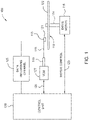
- the spintronic device 230 is electrically coupled to the main pole 220 and the TS 240.
- the main pole 220 and the TS 240 are separated in an area by an insulating layer 272.
- the current source 270 may provide electron current to the spintronic device 230 through the main pole 220 and the TS 240.
- the current source 270 may flow electron current from the main pole 220 through the spintronic device 230 to the TS 240 or may flow electron current from the TS 240 through the spintronic device 230 to the main pole 220 depending on the orientation of the spintronic device 230.
- the spintronic device 230 is coupled to electrical leads providing an electron current other than from the main pole 220 and/or the TS 240.
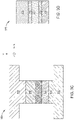
- the first additional sublayer 304a may comprise one of FeCr x , FeV x , FeTi x , FeCr x V y , FeCr x Ti y , FeV x Ti y , or FeCr x V y Ti z , where the value of x is a positive number, and may be a non-integer value or an integer value. While the second sublayer 306 is shown disposed on the first sublayer 304, in some embodiments, the first sublayer 304 is disposed on the second sublayer 306. In such an embodiment, the additional first sublayer 304a may not be included.
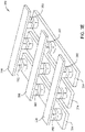
- Figure 3E is a schematic view of certain embodiments of a memory cell array 390 in a cross-point configuration.
- the memory cell array 390 is comprised of a plurality of memory cells 392 formed out of spintronic devices, such as SOT-based MRAM devices.
- each memory cell 392 of the memory cell array 390 comprises the spintronic device 350 of Figure 3B including the multilayer structure 300.
- the memory cells 392 of the memory cell array 390 may comprise other types of spintronic devices comprising the multilayer structure 300 of Figure 3A , such as the spintronic device 360 of Figure 3C .
- the first sublayer 304 comprises FeCr 28
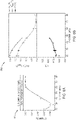
- the second sublayer 306 comprises Co. While the first sublayer 304 comprises FeCr 28 in the embodiment shown in the graph 400, the first sublayer 304 may instead comprise FeV x , FeTi x , FeCr x V y , FeCr x Ti y , FeV x Ti y , FeCr x V y Ti z , or other FeCr x materials discussed above, and the first sublayer 304 is not intended to be limited to only FeCr 28 . Furthermore, the second sublayer 306 may comprise one or more of Cr, V, or Ti as well, as discussed above.
- the first sublayer 304 comprises FeCr 28
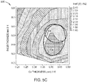
- the second sublayer 306 comprises Co. While the first sublayer 304 comprises FeCr 28 in the embodiment shown in the graph 550, the first sublayer 304 may instead comprise FeV x , FeTi x , FeCr x V y , FeCr x Ti y , FeV x Ti y , FeCr x V y Ti z , or other FeCr x materials discussed above, and similar results would be obtained.
- the second sublayer 306 may comprise one or more of Cr, V, or Ti as well, as discussed above.
- the thickness 314 of the first sublayer 304 is shown on the y-axis
- the thickness 316 of the second sublayer 306 is shown on the x-axis
- the M eff achieved is indicated by the key 592.
- Line 594 illustrates or encompasses an approximate boundary of the thicknesses 314, 316 of the first and second sublayers 304, 306 that achieve the highest M eff .
- the first sublayer 304 having a thickness 314 between about 0.3 nm to about 0.8 nm and the second sublayer 306 having a thickness 316 between about 0.3 nm to about 0.6 nm results in a M eff of about 2.2 T to about 2.6 T.
- Line 596 illustrates or encompasses an approximate boundary of the thicknesses 314, 316 of the first and second sublayers 304, 306 that achieve the highest M eff and the highest negative spin polarization using the data from graph 500 of Figure 5A .
- the first sublayer 304 having a thickness 314 between about 0.4 nm to about 0.6 nm and the second sublayer 306 having a thickness 316 between about 0.35 nm to about 0.5 nm results in the highest M eff and the highest negative spin polarization collectively.
- Figure 6A illustrates a graph 600 showing CIP-GMR ratio in % in the device 350 of Figure 3B utilizing a pinned layer 324 comprising CoFe and the multilayer structure 300 of Figure 3A as the atomic percent (at%) of Cr of the first sublayer 304 comprising FeCr x of the multilayer structure 300 is varied, according to one embodiment.
- the multilayer structure 300 may be within a spintronic device, such as the spintronic device 350 of Figure 3B , the spintronic device 360 of Figure 3C , or the MR sensor 370 of Figure 3D .
- the first sublayer 304 comprises Fe and the second sublayer 306 comprises one of CoCr x , CoV x , CoTi x , CoCr x V y , CoCr x Ti y , CoV x Ti y , or CoCr x V y Ti z , where the value of each of x, y, and/or z in each is a positive number, and may be a non-integer value or an integer value.
- the graph 600 is not intended to be limited to only FeCr x as the material of the first sublayer 304 and Co as the material of the second sublayer 306.
- Each of the first sublayers has a first thickness between about 0.4 nm to about 0.8 nm.
- Each of the second sublayers has a second thickness between about 0.3 nm to about 0.6 nm.
- the multilayer structure is a free layer, a pinned layer, or a field generating layer.
- a magnetic media drive comprises the spintronic device.
- a magnetoresistive random access memory device comprises the spintronic device.
- a magnetic sensor comprises the spintronic device.
- a magnetic recording head comprises the spintronic device.
Landscapes
- Chemical & Material Sciences (AREA)
- Engineering & Computer Science (AREA)
- Materials Engineering (AREA)
- Organic Chemistry (AREA)
- Metallurgy (AREA)
- Mechanical Engineering (AREA)
- Physics & Mathematics (AREA)
- Crystallography & Structural Chemistry (AREA)
- Power Engineering (AREA)
- Computer Hardware Design (AREA)
- General Physics & Mathematics (AREA)
- Condensed Matter Physics & Semiconductors (AREA)
- Manufacturing & Machinery (AREA)
- Hall/Mr Elements (AREA)
Applications Claiming Priority (1)
| Application Number | Priority Date | Filing Date | Title |
|---|---|---|---|
| US17/210,073 US11683993B2 (en) | 2021-03-23 | 2021-03-23 | Material having both negative spin polarization and negative anisotropy |
Publications (2)
| Publication Number | Publication Date |
|---|---|
| EP4064375A1 true EP4064375A1 (de) | 2022-09-28 |
| EP4064375B1 EP4064375B1 (de) | 2024-12-18 |
Family
ID=76355288
Family Applications (1)
| Application Number | Title | Priority Date | Filing Date |
|---|---|---|---|
| EP21178307.1A Active EP4064375B1 (de) | 2021-03-23 | 2021-06-08 | Material mit negativer spin-polarisation und negativer anisotropie |
Country Status (3)
| Country | Link |
|---|---|
| US (1) | US11683993B2 (de) |
| EP (1) | EP4064375B1 (de) |
| CN (1) | CN115116482B (de) |
Citations (2)
| Publication number | Priority date | Publication date | Assignee | Title |
|---|---|---|---|---|
| CN106022345A (zh) * | 2016-04-13 | 2016-10-12 | 杭州远鉴信息科技有限公司 | 一种基于霍夫森林的高压隔离开关状态识别方法 |
| US20200258544A1 (en) | 2019-02-08 | 2020-08-13 | Western Digital Technologies, Inc. | Tape embedded drive |
Family Cites Families (20)
| Publication number | Priority date | Publication date | Assignee | Title |
|---|---|---|---|---|
| US7230265B2 (en) * | 2005-05-16 | 2007-06-12 | International Business Machines Corporation | Spin-polarization devices using rare earth-transition metal alloys |
| CN101752051B (zh) * | 2010-03-05 | 2011-07-20 | 北京科技大学 | 一种垂直磁各向异性多层膜 |
| CN103022345B (zh) * | 2012-12-27 | 2014-09-17 | 河北工业大学 | 一种隧穿磁电阻多层膜材料 |
| US9406315B2 (en) * | 2014-02-12 | 2016-08-02 | HGST Netherlands B.V. | AF-mode STO with negative Hk spin polarization layer |
| WO2015126326A1 (en) | 2014-02-18 | 2015-08-27 | Agency For Science, Technology And Research | Magnetic head with spin torque oscillator for microwave assisted magnetic recording |
| CN104766923B (zh) * | 2015-04-01 | 2017-12-15 | 上海磁宇信息科技有限公司 | 一种三层结构记忆层的磁电阻元件 |
| US9741373B1 (en) * | 2016-04-26 | 2017-08-22 | Tdk Corporation | Microwave assisted magnetic head, head gimbal assembly, and magnetic recording device |
| US9666216B1 (en) | 2016-06-14 | 2017-05-30 | Tdk Corporation | Magnetic recording device and magnetic recording method |
| JP2018133119A (ja) | 2017-02-14 | 2018-08-23 | 株式会社東芝 | 磁気ヘッド、磁気ヘッドアセンブリ、及び磁気記録再生装置 |
| JP2018147540A (ja) * | 2017-03-08 | 2018-09-20 | 株式会社東芝 | 磁気ヘッド及び磁気記録再生装置 |
| US10109302B1 (en) * | 2017-07-18 | 2018-10-23 | Tdk Corporation | Magnetic recording head with spin torque oscillator, head gimbal assembly and magnetic recording apparatus |
| US10762919B1 (en) * | 2018-01-30 | 2020-09-01 | Western Digital Technologies, Inc. | Magnetic recording write head with write pole having a tapered trailing end section with negative magnetic anisotropy |
| US20200105324A1 (en) * | 2018-09-27 | 2020-04-02 | Intel Corporation | Multi-magnet stabilized spin orbit torque mram |
| US10797227B2 (en) | 2018-12-06 | 2020-10-06 | Sandisk Technologies Llc | Spin-transfer torque MRAM with a negative magnetic anisotropy assist layer and methods of operating the same |
| US10643643B1 (en) * | 2019-01-23 | 2020-05-05 | Western Digital Technologies, Inc. | Spin torque oscillator device including a high damping field generation layer or a damping enhancing capping layer |
| JP7379272B2 (ja) * | 2020-06-01 | 2023-11-14 | 株式会社東芝 | 磁気ヘッド及び磁気記録装置 |
| JP7446980B2 (ja) * | 2020-11-19 | 2024-03-11 | 株式会社東芝 | 磁気ヘッド及び磁気記録装置 |
| US11289118B1 (en) * | 2021-01-04 | 2022-03-29 | Western Digital Technologies, Inc. | Spintronic device having negative interface spin scattering |
| JP7465224B2 (ja) * | 2021-02-12 | 2024-04-10 | 株式会社東芝 | 磁気ヘッド及び磁気記録装置 |
| JP7600033B2 (ja) * | 2021-05-28 | 2024-12-16 | 株式会社東芝 | 磁気ヘッド及び磁気記録装置 |
-
2021
- 2021-03-23 US US17/210,073 patent/US11683993B2/en active Active
- 2021-06-08 EP EP21178307.1A patent/EP4064375B1/de active Active
- 2021-06-15 CN CN202110663113.XA patent/CN115116482B/zh active Active
Patent Citations (2)
| Publication number | Priority date | Publication date | Assignee | Title |
|---|---|---|---|---|
| CN106022345A (zh) * | 2016-04-13 | 2016-10-12 | 杭州远鉴信息科技有限公司 | 一种基于霍夫森林的高压隔离开关状态识别方法 |
| US20200258544A1 (en) | 2019-02-08 | 2020-08-13 | Western Digital Technologies, Inc. | Tape embedded drive |
Non-Patent Citations (2)
| Title |
|---|
| FRANK BRÃ1?4SSING ET AL: "Magnetization reversal and magnetic interactions in patterned spin valve structures", JOURNAL OF PHYSICS D: APPLIED PHYSICS, INSTITUTE OF PHYSICS PUBLISHING, BRISTOL, GB, vol. 42, no. 16, 21 August 2009 (2009-08-21), pages 165001, XP020158579, ISSN: 0022-3727 * |
| HIROHATA A ET AL: "Magnetic Properties of Epitaxial Co<tex>$_2$</tex>Cr<tex>$_1-x$</tex>Fe<tex>$_x$</tex>Al Full Heusler Alloy Thin Films With the<tex>$L2_1$</tex>Structure", IEEE TRANSACTIONS ON MAGNETICS, IEEE, USA, vol. 41, no. 10, 1 October 2005 (2005-10-01), pages 2802 - 2804, XP011140654, ISSN: 0018-9464, DOI: 10.1109/TMAG.2005.854831 * |
Also Published As
| Publication number | Publication date |
|---|---|
| US11683993B2 (en) | 2023-06-20 |
| CN115116482A (zh) | 2022-09-27 |
| EP4064375B1 (de) | 2024-12-18 |
| US20220310900A1 (en) | 2022-09-29 |
| CN115116482B (zh) | 2025-09-19 |
Similar Documents
| Publication | Publication Date | Title |
|---|---|---|
| US7283333B2 (en) | Self-pinned double tunnel junction head | |
| US7413636B2 (en) | Method for manufacturing a dual spin valve sensor having a longitudinal bias stack | |
| US9099119B2 (en) | Magnetic read sensor using spin hall effect | |
| JP5173750B2 (ja) | スピントルク発振子、磁気記録ヘッド、磁気ヘッドアセンブリ及び磁気記録装置 | |
| US6657823B2 (en) | Differential detection read sensor, thin film head for perpendicular magnetic recording and perpendicular magnetic recording apparatus | |
| US10157632B1 (en) | Areal density capability improvement with spin-orbit torque based structures surrounding main pole tip | |
| US20220148619A1 (en) | Magnetic Recording Devices Having Negative Polarization Layer To Enhance Spin-Transfer Torque | |
| US20030184919A1 (en) | Dual magnetic tunnel junction sensor with a longitudinal bias stack | |
| US11289118B1 (en) | Spintronic device having negative interface spin scattering | |
| JP2008091842A (ja) | 磁気抵抗効果素子、薄膜磁気ヘッド、ヘッドジンバルアセンブリ、ヘッドアームアセンブリおよび磁気ディスク装置 | |
| US8879214B2 (en) | Half metal trilayer TMR reader with negative interlayer coupling | |
| US8988834B2 (en) | Current perpendicular to plane magnetoresistive sensor employing half metal alloys for improved sensor performance | |
| US10950260B1 (en) | Magnetoresistive sensor with improved magnetic properties and magnetostriction control | |
| JP2008112841A (ja) | 磁気抵抗効果素子、薄膜磁気ヘッド、基体、ウェハ、ヘッドジンバルアセンブリ、ハードディスク装置 | |
| US7268979B2 (en) | Head with thin AFM with high positive magnetostrictive pinned layer | |
| US20250131942A1 (en) | Dynamic DC Field Compensator for MAMR Recording Head | |
| US20060221513A1 (en) | Magnetic read sensor employing oblique etched underlayers for inducing uniaxial magnetic anisotropy in a hard magnetic in-stack bias layer | |
| US7360299B2 (en) | Method for manufacturing a magnetic read sensor employing oblique etched underlayers for inducing uniaxial magnetic anisotropy in a hard magnetic in-stack bias layer | |
| US20080218912A1 (en) | CPP-type magnetoresistive element having spacer layer that includes semiconductor layer | |
| US12040114B2 (en) | Magnetoresistive device comprising a synthetic antiferromagnetic coupling layer of RuAl having a (001) texture | |
| US12207563B2 (en) | Magnetoresistive devices comprising a synthetic antiferromagnetic coupling layer of RuAl having a (110) texture | |
| US11683993B2 (en) | Material having both negative spin polarization and negative anisotropy | |
| US7190560B2 (en) | Self-pinned CPP sensor using Fe/Cr/Fe structure | |
| US20250210241A1 (en) | Spin Orbit Torque (SOT) Device Having a Topological Insulator Layer and a Diffusion Barrier Layer | |
| US12106784B2 (en) | Read sensor with ordered heusler alloy free layer and semiconductor barrier layer |
Legal Events
| Date | Code | Title | Description |
|---|---|---|---|
| PUAI | Public reference made under article 153(3) epc to a published international application that has entered the european phase |
Free format text: ORIGINAL CODE: 0009012 |
|
| STAA | Information on the status of an ep patent application or granted ep patent |
Free format text: STATUS: THE APPLICATION HAS BEEN PUBLISHED |
|
| AK | Designated contracting states |
Kind code of ref document: A1 Designated state(s): AL AT BE BG CH CY CZ DE DK EE ES FI FR GB GR HR HU IE IS IT LI LT LU LV MC MK MT NL NO PL PT RO RS SE SI SK SM TR |
|
| STAA | Information on the status of an ep patent application or granted ep patent |
Free format text: STATUS: REQUEST FOR EXAMINATION WAS MADE |
|
| 17P | Request for examination filed |
Effective date: 20230322 |
|
| RBV | Designated contracting states (corrected) |
Designated state(s): AL AT BE BG CH CY CZ DE DK EE ES FI FR GB GR HR HU IE IS IT LI LT LU LV MC MK MT NL NO PL PT RO RS SE SI SK SM TR |
|
| STAA | Information on the status of an ep patent application or granted ep patent |
Free format text: STATUS: EXAMINATION IS IN PROGRESS |
|
| 17Q | First examination report despatched |
Effective date: 20231025 |
|
| REG | Reference to a national code |
Free format text: PREVIOUS MAIN CLASS: H01L0043100000 Ref country code: DE Ref legal event code: R079 Ref document number: 602021023450 Country of ref document: DE Free format text: PREVIOUS MAIN CLASS: H01L0043100000 Ipc: G11C0011160000 |
|
| GRAP | Despatch of communication of intention to grant a patent |
Free format text: ORIGINAL CODE: EPIDOSNIGR1 |
|
| STAA | Information on the status of an ep patent application or granted ep patent |
Free format text: STATUS: GRANT OF PATENT IS INTENDED |
|
| RIC1 | Information provided on ipc code assigned before grant |
Ipc: G01R 33/09 20060101ALI20240618BHEP Ipc: G01R 33/00 20060101ALI20240618BHEP Ipc: G11C 11/18 20060101ALI20240618BHEP Ipc: H10N 50/85 20230101ALI20240618BHEP Ipc: H10N 50/10 20230101ALI20240618BHEP Ipc: H01F 10/32 20060101ALI20240618BHEP Ipc: G11C 11/16 20060101AFI20240618BHEP |
|
| INTG | Intention to grant announced |
Effective date: 20240722 |
|
| P01 | Opt-out of the competence of the unified patent court (upc) registered |
Free format text: CASE NUMBER: APP_44668/2024 Effective date: 20240801 |
|
| GRAS | Grant fee paid |
Free format text: ORIGINAL CODE: EPIDOSNIGR3 |
|
| GRAA | (expected) grant |
Free format text: ORIGINAL CODE: 0009210 |
|
| STAA | Information on the status of an ep patent application or granted ep patent |
Free format text: STATUS: THE PATENT HAS BEEN GRANTED |
|
| AK | Designated contracting states |
Kind code of ref document: B1 Designated state(s): AL AT BE BG CH CY CZ DE DK EE ES FI FR GB GR HR HU IE IS IT LI LT LU LV MC MK MT NL NO PL PT RO RS SE SI SK SM TR |
|
| REG | Reference to a national code |
Ref country code: CH Ref legal event code: EP |
|
| REG | Reference to a national code |
Ref country code: DE Ref legal event code: R096 Ref document number: 602021023450 Country of ref document: DE |
|
| REG | Reference to a national code |
Ref country code: IE Ref legal event code: FG4D |
|
| REG | Reference to a national code |
Ref country code: LT Ref legal event code: MG9D |
|
| PG25 | Lapsed in a contracting state [announced via postgrant information from national office to epo] |
Ref country code: HR Free format text: LAPSE BECAUSE OF FAILURE TO SUBMIT A TRANSLATION OF THE DESCRIPTION OR TO PAY THE FEE WITHIN THE PRESCRIBED TIME-LIMIT Effective date: 20241218 |
|
| PG25 | Lapsed in a contracting state [announced via postgrant information from national office to epo] |
Ref country code: FI Free format text: LAPSE BECAUSE OF FAILURE TO SUBMIT A TRANSLATION OF THE DESCRIPTION OR TO PAY THE FEE WITHIN THE PRESCRIBED TIME-LIMIT Effective date: 20241218 |
|
| PG25 | Lapsed in a contracting state [announced via postgrant information from national office to epo] |
Ref country code: BG Free format text: LAPSE BECAUSE OF FAILURE TO SUBMIT A TRANSLATION OF THE DESCRIPTION OR TO PAY THE FEE WITHIN THE PRESCRIBED TIME-LIMIT Effective date: 20241218 |
|
| PG25 | Lapsed in a contracting state [announced via postgrant information from national office to epo] |
Ref country code: NO Free format text: LAPSE BECAUSE OF FAILURE TO SUBMIT A TRANSLATION OF THE DESCRIPTION OR TO PAY THE FEE WITHIN THE PRESCRIBED TIME-LIMIT Effective date: 20250318 |
|
| REG | Reference to a national code |
Ref country code: NL Ref legal event code: MP Effective date: 20241218 |
|
| PG25 | Lapsed in a contracting state [announced via postgrant information from national office to epo] |
Ref country code: GR Free format text: LAPSE BECAUSE OF FAILURE TO SUBMIT A TRANSLATION OF THE DESCRIPTION OR TO PAY THE FEE WITHIN THE PRESCRIBED TIME-LIMIT Effective date: 20250319 Ref country code: LV Free format text: LAPSE BECAUSE OF FAILURE TO SUBMIT A TRANSLATION OF THE DESCRIPTION OR TO PAY THE FEE WITHIN THE PRESCRIBED TIME-LIMIT Effective date: 20241218 |
|
| PG25 | Lapsed in a contracting state [announced via postgrant information from national office to epo] |
Ref country code: RS Free format text: LAPSE BECAUSE OF FAILURE TO SUBMIT A TRANSLATION OF THE DESCRIPTION OR TO PAY THE FEE WITHIN THE PRESCRIBED TIME-LIMIT Effective date: 20250318 |
|
| PG25 | Lapsed in a contracting state [announced via postgrant information from national office to epo] |
Ref country code: NL Free format text: LAPSE BECAUSE OF FAILURE TO SUBMIT A TRANSLATION OF THE DESCRIPTION OR TO PAY THE FEE WITHIN THE PRESCRIBED TIME-LIMIT Effective date: 20241218 |
|
| REG | Reference to a national code |
Ref country code: AT Ref legal event code: MK05 Ref document number: 1752926 Country of ref document: AT Kind code of ref document: T Effective date: 20241218 |
|
| PG25 | Lapsed in a contracting state [announced via postgrant information from national office to epo] |
Ref country code: SM Free format text: LAPSE BECAUSE OF FAILURE TO SUBMIT A TRANSLATION OF THE DESCRIPTION OR TO PAY THE FEE WITHIN THE PRESCRIBED TIME-LIMIT Effective date: 20241218 |
|
| PG25 | Lapsed in a contracting state [announced via postgrant information from national office to epo] |
Ref country code: PL Free format text: LAPSE BECAUSE OF FAILURE TO SUBMIT A TRANSLATION OF THE DESCRIPTION OR TO PAY THE FEE WITHIN THE PRESCRIBED TIME-LIMIT Effective date: 20241218 |
|
| PGFP | Annual fee paid to national office [announced via postgrant information from national office to epo] |
Ref country code: DE Payment date: 20250429 Year of fee payment: 5 |
|
| PG25 | Lapsed in a contracting state [announced via postgrant information from national office to epo] |
Ref country code: ES Free format text: LAPSE BECAUSE OF FAILURE TO SUBMIT A TRANSLATION OF THE DESCRIPTION OR TO PAY THE FEE WITHIN THE PRESCRIBED TIME-LIMIT Effective date: 20241218 |
|
| PGFP | Annual fee paid to national office [announced via postgrant information from national office to epo] |
Ref country code: GB Payment date: 20250501 Year of fee payment: 5 |
|
| PG25 | Lapsed in a contracting state [announced via postgrant information from national office to epo] |
Ref country code: IS Free format text: LAPSE BECAUSE OF FAILURE TO SUBMIT A TRANSLATION OF THE DESCRIPTION OR TO PAY THE FEE WITHIN THE PRESCRIBED TIME-LIMIT Effective date: 20250418 |
|
| PG25 | Lapsed in a contracting state [announced via postgrant information from national office to epo] |
Ref country code: PT Free format text: LAPSE BECAUSE OF FAILURE TO SUBMIT A TRANSLATION OF THE DESCRIPTION OR TO PAY THE FEE WITHIN THE PRESCRIBED TIME-LIMIT Effective date: 20250421 |
|
| PG25 | Lapsed in a contracting state [announced via postgrant information from national office to epo] |
Ref country code: EE Free format text: LAPSE BECAUSE OF FAILURE TO SUBMIT A TRANSLATION OF THE DESCRIPTION OR TO PAY THE FEE WITHIN THE PRESCRIBED TIME-LIMIT Effective date: 20241218 |
|
| PG25 | Lapsed in a contracting state [announced via postgrant information from national office to epo] |
Ref country code: AT Free format text: LAPSE BECAUSE OF FAILURE TO SUBMIT A TRANSLATION OF THE DESCRIPTION OR TO PAY THE FEE WITHIN THE PRESCRIBED TIME-LIMIT Effective date: 20241218 Ref country code: RO Free format text: LAPSE BECAUSE OF FAILURE TO SUBMIT A TRANSLATION OF THE DESCRIPTION OR TO PAY THE FEE WITHIN THE PRESCRIBED TIME-LIMIT Effective date: 20241218 |
|
| PG25 | Lapsed in a contracting state [announced via postgrant information from national office to epo] |
Ref country code: SK Free format text: LAPSE BECAUSE OF FAILURE TO SUBMIT A TRANSLATION OF THE DESCRIPTION OR TO PAY THE FEE WITHIN THE PRESCRIBED TIME-LIMIT Effective date: 20241218 |
|
| PG25 | Lapsed in a contracting state [announced via postgrant information from national office to epo] |
Ref country code: CZ Free format text: LAPSE BECAUSE OF FAILURE TO SUBMIT A TRANSLATION OF THE DESCRIPTION OR TO PAY THE FEE WITHIN THE PRESCRIBED TIME-LIMIT Effective date: 20241218 |
|
| PG25 | Lapsed in a contracting state [announced via postgrant information from national office to epo] |
Ref country code: IT Free format text: LAPSE BECAUSE OF FAILURE TO SUBMIT A TRANSLATION OF THE DESCRIPTION OR TO PAY THE FEE WITHIN THE PRESCRIBED TIME-LIMIT Effective date: 20241218 |
|
| PG25 | Lapsed in a contracting state [announced via postgrant information from national office to epo] |
Ref country code: SE Free format text: LAPSE BECAUSE OF FAILURE TO SUBMIT A TRANSLATION OF THE DESCRIPTION OR TO PAY THE FEE WITHIN THE PRESCRIBED TIME-LIMIT Effective date: 20241218 |
|
| REG | Reference to a national code |
Ref country code: DE Ref legal event code: R097 Ref document number: 602021023450 Country of ref document: DE |
|
| PG25 | Lapsed in a contracting state [announced via postgrant information from national office to epo] |
Ref country code: DK Free format text: LAPSE BECAUSE OF FAILURE TO SUBMIT A TRANSLATION OF THE DESCRIPTION OR TO PAY THE FEE WITHIN THE PRESCRIBED TIME-LIMIT Effective date: 20241218 |
|
| PLBE | No opposition filed within time limit |
Free format text: ORIGINAL CODE: 0009261 |
|
| STAA | Information on the status of an ep patent application or granted ep patent |
Free format text: STATUS: NO OPPOSITION FILED WITHIN TIME LIMIT |
|
| REG | Reference to a national code |
Ref country code: CH Ref legal event code: L10 Free format text: ST27 STATUS EVENT CODE: U-0-0-L10-L00 (AS PROVIDED BY THE NATIONAL OFFICE) Effective date: 20251029 |
|
| 26N | No opposition filed |
Effective date: 20250919 |
|
| REG | Reference to a national code |
Ref country code: CH Ref legal event code: H13 Free format text: ST27 STATUS EVENT CODE: U-0-0-H10-H13 (AS PROVIDED BY THE NATIONAL OFFICE) Effective date: 20260127 |
|
| PG25 | Lapsed in a contracting state [announced via postgrant information from national office to epo] |
Ref country code: MC Free format text: LAPSE BECAUSE OF FAILURE TO SUBMIT A TRANSLATION OF THE DESCRIPTION OR TO PAY THE FEE WITHIN THE PRESCRIBED TIME-LIMIT Effective date: 20241218 |
|
| PG25 | Lapsed in a contracting state [announced via postgrant information from national office to epo] |
Ref country code: LU Free format text: LAPSE BECAUSE OF NON-PAYMENT OF DUE FEES Effective date: 20250608 |
|
| REG | Reference to a national code |
Ref country code: BE Ref legal event code: MM Effective date: 20250630 |
|
| PG25 | Lapsed in a contracting state [announced via postgrant information from national office to epo] |
Ref country code: IE Free format text: LAPSE BECAUSE OF NON-PAYMENT OF DUE FEES Effective date: 20250608 |
|
| PG25 | Lapsed in a contracting state [announced via postgrant information from national office to epo] |
Ref country code: BE Free format text: LAPSE BECAUSE OF NON-PAYMENT OF DUE FEES Effective date: 20250630 |
|
| PG25 | Lapsed in a contracting state [announced via postgrant information from national office to epo] |
Ref country code: FR Free format text: LAPSE BECAUSE OF NON-PAYMENT OF DUE FEES Effective date: 20250630 |
|
| PG25 | Lapsed in a contracting state [announced via postgrant information from national office to epo] |
Ref country code: CH Free format text: LAPSE BECAUSE OF NON-PAYMENT OF DUE FEES Effective date: 20250630 |