EP4064264A2 - Anzeigevorrichtung - Google Patents
Anzeigevorrichtung Download PDFInfo
- Publication number
- EP4064264A2 EP4064264A2 EP22161295.5A EP22161295A EP4064264A2 EP 4064264 A2 EP4064264 A2 EP 4064264A2 EP 22161295 A EP22161295 A EP 22161295A EP 4064264 A2 EP4064264 A2 EP 4064264A2
- Authority
- EP
- European Patent Office
- Prior art keywords
- transistor
- scan
- voltage
- line
- signal
- Prior art date
- Legal status (The legal status is an assumption and is not a legal conclusion. Google has not performed a legal analysis and makes no representation as to the accuracy of the status listed.)
- Pending
Links
Images









Classifications
-
- G—PHYSICS
- G09—EDUCATION; CRYPTOGRAPHY; DISPLAY; ADVERTISING; SEALS
- G09G—ARRANGEMENTS OR CIRCUITS FOR CONTROL OF INDICATING DEVICES USING STATIC MEANS TO PRESENT VARIABLE INFORMATION
- G09G3/00—Control arrangements or circuits, of interest only in connection with visual indicators other than cathode-ray tubes
- G09G3/20—Control arrangements or circuits, of interest only in connection with visual indicators other than cathode-ray tubes for presentation of an assembly of a number of characters, e.g. a page, by composing the assembly by combination of individual elements arranged in a matrix no fixed position being assigned to or needed to be assigned to the individual characters or partial characters
- G09G3/22—Control arrangements or circuits, of interest only in connection with visual indicators other than cathode-ray tubes for presentation of an assembly of a number of characters, e.g. a page, by composing the assembly by combination of individual elements arranged in a matrix no fixed position being assigned to or needed to be assigned to the individual characters or partial characters using controlled light sources
- G09G3/30—Control arrangements or circuits, of interest only in connection with visual indicators other than cathode-ray tubes for presentation of an assembly of a number of characters, e.g. a page, by composing the assembly by combination of individual elements arranged in a matrix no fixed position being assigned to or needed to be assigned to the individual characters or partial characters using controlled light sources using electroluminescent panels
- G09G3/32—Control arrangements or circuits, of interest only in connection with visual indicators other than cathode-ray tubes for presentation of an assembly of a number of characters, e.g. a page, by composing the assembly by combination of individual elements arranged in a matrix no fixed position being assigned to or needed to be assigned to the individual characters or partial characters using controlled light sources using electroluminescent panels semiconductive, e.g. using light-emitting diodes [LED]
- G09G3/3208—Control arrangements or circuits, of interest only in connection with visual indicators other than cathode-ray tubes for presentation of an assembly of a number of characters, e.g. a page, by composing the assembly by combination of individual elements arranged in a matrix no fixed position being assigned to or needed to be assigned to the individual characters or partial characters using controlled light sources using electroluminescent panels semiconductive, e.g. using light-emitting diodes [LED] organic, e.g. using organic light-emitting diodes [OLED]
- G09G3/3266—Details of drivers for scan electrodes
-
- G—PHYSICS
- G09—EDUCATION; CRYPTOGRAPHY; DISPLAY; ADVERTISING; SEALS
- G09G—ARRANGEMENTS OR CIRCUITS FOR CONTROL OF INDICATING DEVICES USING STATIC MEANS TO PRESENT VARIABLE INFORMATION
- G09G3/00—Control arrangements or circuits, of interest only in connection with visual indicators other than cathode-ray tubes
- G09G3/20—Control arrangements or circuits, of interest only in connection with visual indicators other than cathode-ray tubes for presentation of an assembly of a number of characters, e.g. a page, by composing the assembly by combination of individual elements arranged in a matrix no fixed position being assigned to or needed to be assigned to the individual characters or partial characters
- G09G3/22—Control arrangements or circuits, of interest only in connection with visual indicators other than cathode-ray tubes for presentation of an assembly of a number of characters, e.g. a page, by composing the assembly by combination of individual elements arranged in a matrix no fixed position being assigned to or needed to be assigned to the individual characters or partial characters using controlled light sources
- G09G3/30—Control arrangements or circuits, of interest only in connection with visual indicators other than cathode-ray tubes for presentation of an assembly of a number of characters, e.g. a page, by composing the assembly by combination of individual elements arranged in a matrix no fixed position being assigned to or needed to be assigned to the individual characters or partial characters using controlled light sources using electroluminescent panels
- G09G3/32—Control arrangements or circuits, of interest only in connection with visual indicators other than cathode-ray tubes for presentation of an assembly of a number of characters, e.g. a page, by composing the assembly by combination of individual elements arranged in a matrix no fixed position being assigned to or needed to be assigned to the individual characters or partial characters using controlled light sources using electroluminescent panels semiconductive, e.g. using light-emitting diodes [LED]
- G09G3/3208—Control arrangements or circuits, of interest only in connection with visual indicators other than cathode-ray tubes for presentation of an assembly of a number of characters, e.g. a page, by composing the assembly by combination of individual elements arranged in a matrix no fixed position being assigned to or needed to be assigned to the individual characters or partial characters using controlled light sources using electroluminescent panels semiconductive, e.g. using light-emitting diodes [LED] organic, e.g. using organic light-emitting diodes [OLED]
- G09G3/3225—Control arrangements or circuits, of interest only in connection with visual indicators other than cathode-ray tubes for presentation of an assembly of a number of characters, e.g. a page, by composing the assembly by combination of individual elements arranged in a matrix no fixed position being assigned to or needed to be assigned to the individual characters or partial characters using controlled light sources using electroluminescent panels semiconductive, e.g. using light-emitting diodes [LED] organic, e.g. using organic light-emitting diodes [OLED] using an active matrix
- G09G3/3233—Control arrangements or circuits, of interest only in connection with visual indicators other than cathode-ray tubes for presentation of an assembly of a number of characters, e.g. a page, by composing the assembly by combination of individual elements arranged in a matrix no fixed position being assigned to or needed to be assigned to the individual characters or partial characters using controlled light sources using electroluminescent panels semiconductive, e.g. using light-emitting diodes [LED] organic, e.g. using organic light-emitting diodes [OLED] using an active matrix with pixel circuitry controlling the current through the light-emitting element
-
- G—PHYSICS
- G09—EDUCATION; CRYPTOGRAPHY; DISPLAY; ADVERTISING; SEALS
- G09G—ARRANGEMENTS OR CIRCUITS FOR CONTROL OF INDICATING DEVICES USING STATIC MEANS TO PRESENT VARIABLE INFORMATION
- G09G3/00—Control arrangements or circuits, of interest only in connection with visual indicators other than cathode-ray tubes
- G09G3/20—Control arrangements or circuits, of interest only in connection with visual indicators other than cathode-ray tubes for presentation of an assembly of a number of characters, e.g. a page, by composing the assembly by combination of individual elements arranged in a matrix no fixed position being assigned to or needed to be assigned to the individual characters or partial characters
- G09G3/22—Control arrangements or circuits, of interest only in connection with visual indicators other than cathode-ray tubes for presentation of an assembly of a number of characters, e.g. a page, by composing the assembly by combination of individual elements arranged in a matrix no fixed position being assigned to or needed to be assigned to the individual characters or partial characters using controlled light sources
- G09G3/30—Control arrangements or circuits, of interest only in connection with visual indicators other than cathode-ray tubes for presentation of an assembly of a number of characters, e.g. a page, by composing the assembly by combination of individual elements arranged in a matrix no fixed position being assigned to or needed to be assigned to the individual characters or partial characters using controlled light sources using electroluminescent panels
- G09G3/32—Control arrangements or circuits, of interest only in connection with visual indicators other than cathode-ray tubes for presentation of an assembly of a number of characters, e.g. a page, by composing the assembly by combination of individual elements arranged in a matrix no fixed position being assigned to or needed to be assigned to the individual characters or partial characters using controlled light sources using electroluminescent panels semiconductive, e.g. using light-emitting diodes [LED]
- G09G3/3208—Control arrangements or circuits, of interest only in connection with visual indicators other than cathode-ray tubes for presentation of an assembly of a number of characters, e.g. a page, by composing the assembly by combination of individual elements arranged in a matrix no fixed position being assigned to or needed to be assigned to the individual characters or partial characters using controlled light sources using electroluminescent panels semiconductive, e.g. using light-emitting diodes [LED] organic, e.g. using organic light-emitting diodes [OLED]
- G09G3/3225—Control arrangements or circuits, of interest only in connection with visual indicators other than cathode-ray tubes for presentation of an assembly of a number of characters, e.g. a page, by composing the assembly by combination of individual elements arranged in a matrix no fixed position being assigned to or needed to be assigned to the individual characters or partial characters using controlled light sources using electroluminescent panels semiconductive, e.g. using light-emitting diodes [LED] organic, e.g. using organic light-emitting diodes [OLED] using an active matrix
- G09G3/3258—Control arrangements or circuits, of interest only in connection with visual indicators other than cathode-ray tubes for presentation of an assembly of a number of characters, e.g. a page, by composing the assembly by combination of individual elements arranged in a matrix no fixed position being assigned to or needed to be assigned to the individual characters or partial characters using controlled light sources using electroluminescent panels semiconductive, e.g. using light-emitting diodes [LED] organic, e.g. using organic light-emitting diodes [OLED] using an active matrix with pixel circuitry controlling the voltage across the light-emitting element
-
- G—PHYSICS
- G09—EDUCATION; CRYPTOGRAPHY; DISPLAY; ADVERTISING; SEALS
- G09G—ARRANGEMENTS OR CIRCUITS FOR CONTROL OF INDICATING DEVICES USING STATIC MEANS TO PRESENT VARIABLE INFORMATION
- G09G3/00—Control arrangements or circuits, of interest only in connection with visual indicators other than cathode-ray tubes
- G09G3/20—Control arrangements or circuits, of interest only in connection with visual indicators other than cathode-ray tubes for presentation of an assembly of a number of characters, e.g. a page, by composing the assembly by combination of individual elements arranged in a matrix no fixed position being assigned to or needed to be assigned to the individual characters or partial characters
- G09G3/22—Control arrangements or circuits, of interest only in connection with visual indicators other than cathode-ray tubes for presentation of an assembly of a number of characters, e.g. a page, by composing the assembly by combination of individual elements arranged in a matrix no fixed position being assigned to or needed to be assigned to the individual characters or partial characters using controlled light sources
- G09G3/30—Control arrangements or circuits, of interest only in connection with visual indicators other than cathode-ray tubes for presentation of an assembly of a number of characters, e.g. a page, by composing the assembly by combination of individual elements arranged in a matrix no fixed position being assigned to or needed to be assigned to the individual characters or partial characters using controlled light sources using electroluminescent panels
- G09G3/32—Control arrangements or circuits, of interest only in connection with visual indicators other than cathode-ray tubes for presentation of an assembly of a number of characters, e.g. a page, by composing the assembly by combination of individual elements arranged in a matrix no fixed position being assigned to or needed to be assigned to the individual characters or partial characters using controlled light sources using electroluminescent panels semiconductive, e.g. using light-emitting diodes [LED]
- G09G3/3208—Control arrangements or circuits, of interest only in connection with visual indicators other than cathode-ray tubes for presentation of an assembly of a number of characters, e.g. a page, by composing the assembly by combination of individual elements arranged in a matrix no fixed position being assigned to or needed to be assigned to the individual characters or partial characters using controlled light sources using electroluminescent panels semiconductive, e.g. using light-emitting diodes [LED] organic, e.g. using organic light-emitting diodes [OLED]
- G09G3/3225—Control arrangements or circuits, of interest only in connection with visual indicators other than cathode-ray tubes for presentation of an assembly of a number of characters, e.g. a page, by composing the assembly by combination of individual elements arranged in a matrix no fixed position being assigned to or needed to be assigned to the individual characters or partial characters using controlled light sources using electroluminescent panels semiconductive, e.g. using light-emitting diodes [LED] organic, e.g. using organic light-emitting diodes [OLED] using an active matrix
-
- G—PHYSICS
- G09—EDUCATION; CRYPTOGRAPHY; DISPLAY; ADVERTISING; SEALS
- G09G—ARRANGEMENTS OR CIRCUITS FOR CONTROL OF INDICATING DEVICES USING STATIC MEANS TO PRESENT VARIABLE INFORMATION
- G09G2300/00—Aspects of the constitution of display devices
- G09G2300/04—Structural and physical details of display devices
- G09G2300/0421—Structural details of the set of electrodes
- G09G2300/0426—Layout of electrodes and connections
-
- G—PHYSICS
- G09—EDUCATION; CRYPTOGRAPHY; DISPLAY; ADVERTISING; SEALS
- G09G—ARRANGEMENTS OR CIRCUITS FOR CONTROL OF INDICATING DEVICES USING STATIC MEANS TO PRESENT VARIABLE INFORMATION
- G09G2300/00—Aspects of the constitution of display devices
- G09G2300/08—Active matrix structure, i.e. with use of active elements, inclusive of non-linear two terminal elements, in the pixels together with light emitting or modulating elements
- G09G2300/0809—Several active elements per pixel in active matrix panels
- G09G2300/0819—Several active elements per pixel in active matrix panels used for counteracting undesired variations, e.g. feedback or autozeroing
-
- G—PHYSICS
- G09—EDUCATION; CRYPTOGRAPHY; DISPLAY; ADVERTISING; SEALS
- G09G—ARRANGEMENTS OR CIRCUITS FOR CONTROL OF INDICATING DEVICES USING STATIC MEANS TO PRESENT VARIABLE INFORMATION
- G09G2300/00—Aspects of the constitution of display devices
- G09G2300/08—Active matrix structure, i.e. with use of active elements, inclusive of non-linear two terminal elements, in the pixels together with light emitting or modulating elements
- G09G2300/0809—Several active elements per pixel in active matrix panels
- G09G2300/0842—Several active elements per pixel in active matrix panels forming a memory circuit, e.g. a dynamic memory with one capacitor
-
- G—PHYSICS
- G09—EDUCATION; CRYPTOGRAPHY; DISPLAY; ADVERTISING; SEALS
- G09G—ARRANGEMENTS OR CIRCUITS FOR CONTROL OF INDICATING DEVICES USING STATIC MEANS TO PRESENT VARIABLE INFORMATION
- G09G2300/00—Aspects of the constitution of display devices
- G09G2300/08—Active matrix structure, i.e. with use of active elements, inclusive of non-linear two terminal elements, in the pixels together with light emitting or modulating elements
- G09G2300/0809—Several active elements per pixel in active matrix panels
- G09G2300/0842—Several active elements per pixel in active matrix panels forming a memory circuit, e.g. a dynamic memory with one capacitor
- G09G2300/0861—Several active elements per pixel in active matrix panels forming a memory circuit, e.g. a dynamic memory with one capacitor with additional control of the display period without amending the charge stored in a pixel memory, e.g. by means of additional select electrodes
-
- G—PHYSICS
- G09—EDUCATION; CRYPTOGRAPHY; DISPLAY; ADVERTISING; SEALS
- G09G—ARRANGEMENTS OR CIRCUITS FOR CONTROL OF INDICATING DEVICES USING STATIC MEANS TO PRESENT VARIABLE INFORMATION
- G09G2310/00—Command of the display device
- G09G2310/02—Addressing, scanning or driving the display screen or processing steps related thereto
- G09G2310/0243—Details of the generation of driving signals
- G09G2310/0251—Precharge or discharge of pixel before applying new pixel voltage
-
- G—PHYSICS
- G09—EDUCATION; CRYPTOGRAPHY; DISPLAY; ADVERTISING; SEALS
- G09G—ARRANGEMENTS OR CIRCUITS FOR CONTROL OF INDICATING DEVICES USING STATIC MEANS TO PRESENT VARIABLE INFORMATION
- G09G2310/00—Command of the display device
- G09G2310/02—Addressing, scanning or driving the display screen or processing steps related thereto
- G09G2310/0262—The addressing of the pixel, in a display other than an active matrix LCD, involving the control of two or more scan electrodes or two or more data electrodes, e.g. pixel voltage dependent on signals of two data electrodes
-
- G—PHYSICS
- G09—EDUCATION; CRYPTOGRAPHY; DISPLAY; ADVERTISING; SEALS
- G09G—ARRANGEMENTS OR CIRCUITS FOR CONTROL OF INDICATING DEVICES USING STATIC MEANS TO PRESENT VARIABLE INFORMATION
- G09G2310/00—Command of the display device
- G09G2310/02—Addressing, scanning or driving the display screen or processing steps related thereto
- G09G2310/0264—Details of driving circuits
-
- G—PHYSICS
- G09—EDUCATION; CRYPTOGRAPHY; DISPLAY; ADVERTISING; SEALS
- G09G—ARRANGEMENTS OR CIRCUITS FOR CONTROL OF INDICATING DEVICES USING STATIC MEANS TO PRESENT VARIABLE INFORMATION
- G09G2310/00—Command of the display device
- G09G2310/02—Addressing, scanning or driving the display screen or processing steps related thereto
- G09G2310/0264—Details of driving circuits
- G09G2310/0278—Details of driving circuits arranged to drive both scan and data electrodes
-
- G—PHYSICS
- G09—EDUCATION; CRYPTOGRAPHY; DISPLAY; ADVERTISING; SEALS
- G09G—ARRANGEMENTS OR CIRCUITS FOR CONTROL OF INDICATING DEVICES USING STATIC MEANS TO PRESENT VARIABLE INFORMATION
- G09G2310/00—Command of the display device
- G09G2310/02—Addressing, scanning or driving the display screen or processing steps related thereto
- G09G2310/0264—Details of driving circuits
- G09G2310/0286—Details of a shift registers arranged for use in a driving circuit
-
- G—PHYSICS
- G09—EDUCATION; CRYPTOGRAPHY; DISPLAY; ADVERTISING; SEALS
- G09G—ARRANGEMENTS OR CIRCUITS FOR CONTROL OF INDICATING DEVICES USING STATIC MEANS TO PRESENT VARIABLE INFORMATION
- G09G2310/00—Command of the display device
- G09G2310/06—Details of flat display driving waveforms
- G09G2310/061—Details of flat display driving waveforms for resetting or blanking
-
- G—PHYSICS
- G09—EDUCATION; CRYPTOGRAPHY; DISPLAY; ADVERTISING; SEALS
- G09G—ARRANGEMENTS OR CIRCUITS FOR CONTROL OF INDICATING DEVICES USING STATIC MEANS TO PRESENT VARIABLE INFORMATION
- G09G2310/00—Command of the display device
- G09G2310/08—Details of timing specific for flat panels, other than clock recovery
-
- G—PHYSICS
- G09—EDUCATION; CRYPTOGRAPHY; DISPLAY; ADVERTISING; SEALS
- G09G—ARRANGEMENTS OR CIRCUITS FOR CONTROL OF INDICATING DEVICES USING STATIC MEANS TO PRESENT VARIABLE INFORMATION
- G09G2320/00—Control of display operating conditions
- G09G2320/02—Improving the quality of display appearance
- G09G2320/0209—Crosstalk reduction, i.e. to reduce direct or indirect influences of signals directed to a certain pixel of the displayed image on other pixels of said image, inclusive of influences affecting pixels in different frames or fields or sub-images which constitute a same image, e.g. left and right images of a stereoscopic display
-
- G—PHYSICS
- G09—EDUCATION; CRYPTOGRAPHY; DISPLAY; ADVERTISING; SEALS
- G09G—ARRANGEMENTS OR CIRCUITS FOR CONTROL OF INDICATING DEVICES USING STATIC MEANS TO PRESENT VARIABLE INFORMATION
- G09G2320/00—Control of display operating conditions
- G09G2320/02—Improving the quality of display appearance
- G09G2320/0219—Reducing feedthrough effects in active matrix panels, i.e. voltage changes on the scan electrode influencing the pixel voltage due to capacitive coupling
-
- G—PHYSICS
- G09—EDUCATION; CRYPTOGRAPHY; DISPLAY; ADVERTISING; SEALS
- G09G—ARRANGEMENTS OR CIRCUITS FOR CONTROL OF INDICATING DEVICES USING STATIC MEANS TO PRESENT VARIABLE INFORMATION
- G09G2320/00—Control of display operating conditions
- G09G2320/02—Improving the quality of display appearance
- G09G2320/0223—Compensation for problems related to R-C delay and attenuation in electrodes of matrix panels, e.g. in gate electrodes or on-substrate video signal electrodes
-
- G—PHYSICS
- G09—EDUCATION; CRYPTOGRAPHY; DISPLAY; ADVERTISING; SEALS
- G09G—ARRANGEMENTS OR CIRCUITS FOR CONTROL OF INDICATING DEVICES USING STATIC MEANS TO PRESENT VARIABLE INFORMATION
- G09G2330/00—Aspects of power supply; Aspects of display protection and defect management
-
- G—PHYSICS
- G09—EDUCATION; CRYPTOGRAPHY; DISPLAY; ADVERTISING; SEALS
- G09G—ARRANGEMENTS OR CIRCUITS FOR CONTROL OF INDICATING DEVICES USING STATIC MEANS TO PRESENT VARIABLE INFORMATION
- G09G2330/00—Aspects of power supply; Aspects of display protection and defect management
- G09G2330/02—Details of power systems and of start or stop of display operation
- G09G2330/021—Power management, e.g. power saving
-
- G—PHYSICS
- G09—EDUCATION; CRYPTOGRAPHY; DISPLAY; ADVERTISING; SEALS
- G09G—ARRANGEMENTS OR CIRCUITS FOR CONTROL OF INDICATING DEVICES USING STATIC MEANS TO PRESENT VARIABLE INFORMATION
- G09G2330/00—Aspects of power supply; Aspects of display protection and defect management
- G09G2330/02—Details of power systems and of start or stop of display operation
- G09G2330/028—Generation of voltages supplied to electrode drivers in a matrix display other than LCD
Definitions
- the disclosure relates to a display device.
- display devices are employed in various electronic devices such as smartphones, digital cameras, laptop computers, navigation devices, and smart televisions.
- the display device there are a liquid crystal display device, a field emission display device, an organic light emitting display device, and the like.
- the organic light emitting display device may include a light emitting element in which each pixel of a display panel may emit light by itself, a driving transistor that controls the amount of driving current supplied from a power line to the light emitting element according to a data voltage of a data line applied to a gate electrode, and transistors that act as a switch by being turned on or off according to a scan signal of a scan line and an emission signal of an emission line.
- the voltage of the scan line may be affected according to the change in the data voltage of the data line, and thus the voltage of the gate electrode of the driving transistor may fluctuate.
- the voltage of the gate electrode of the driving transistor fluctuates, it is difficult for the light emitting element to emit light with a desired luminance.
- aspects of the disclosure provide a display device capable of preventing a voltage of a gate electrode of a driving transistor from fluctuating.
- a display device may include a plurality of sub-pixels electrically connected to first scan lines, second scan lines, and emission lines, a first scan driver that applies first scan signals to the first scan lines, a second scan driver that applies second scan signals to the second scan lines, an emission control driver that applies emission signals to the emission lines, and a power supply that generates and outputs a first high voltage and a second high voltage.
- the second scan driver may receive the first high voltage.
- the first scan driver and the emission control driver share the second high voltage.
- the definition that at least two elements share a voltage especially means that the at least two elements are electrically connected in parallel to a corresponding power supply applying the voltage to the at least two elements.
- the voltage applied to the at least two elements is therefore the same.
- the display device may further comprise third scan lines, and a third scan driver that applies third scan signals to the third scan lines.
- the third scan driver may receive the second high voltage.
- the display device may further comprise fourth scan lines, and a fourth scan driver that applies fourth scan signals to the fourth scan lines.
- the fourth scan driver may receive the second high voltage.
- the display device may further comprise fourth scan lines, and a fourth scan driver that applies fourth scan signals to the fourth scan lines.
- the fourth scan driver may receive the first high voltage.
- the power supply may generate and output a first low voltage and a second low voltage.
- the first scan driver and the third scan driver may share the second low voltage.
- the second scan driver, the fourth scan driver, and the emission control driver may share the first low voltage.
- the display device may further comprise a display area in which the plurality of sub-pixels are disposed and display an image, and a non-display area disposed adjacent the display area.
- the second scan driver may comprise a first sub-scan driver that applies second scan signals to the second scan lines and is disposed on a side of the non-display area, and a second sub-scan driver that applies second scan signals to the second scan lines and is disposed on another side opposite to one side of the non-display area.
- the first scan driver and the emission control driver may be disposed on the side of the non-display area.
- the third scan driver and the fourth scan driver may be disposed on the another side of the non-display area.
- the third scan driver and the emission control driver may be disposed on the side of the non-display area.
- the first scan driver and the fourth scan driver may be disposed on the another side of the non-display area.
- the display device may further comprise data lines, a first driving voltage line, and a first initialization voltage line electrically connected to each of the plurality of sub-pixels.
- Each of the plurality of sub-pixels may comprise a light emitting element, a first transistor that applies a driving current to the light emitting element according to a voltage of a gate electrode, a second transistor that applies a data voltage of the data line to a first electrode of the first transistor according to a second scan signal of the second scan line, a third transistor that initializes the gate electrode of the first transistor to a first initialization voltage of the first initialization voltage line according to a first scan signal of the first scan line, and a fourth transistor that electrically connects the first driving voltage line and the first electrode of the first transistor according to the emission signal of the emission line.
- the display device may further comprise a second initialization voltage line electrically connected to each of the plurality of sub-pixels.
- Each of the plurality of sub-pixels may further comprise a fifth transistor that electrically connects the gate electrode and a second electrode of the first transistor according to a third scan signal of the third scan line, a sixth transistor that initializes an anode electrode of the light emitting element to a second initialization voltage of the second initialization voltage line according to a fourth scan signal of the fourth scan line, and a seventh transistor that electrically connects the second electrode of the first transistor and the anode electrode of the light emitting element according to the emission signal of the emission line.
- Each of the first transistor, the second transistor, the fourth transistor, the sixth transistor, and the seventh transistor may be a P-channel transistor.
- Each of the third transistor and the fifth transistor may be an N-channel transistor.
- Each of the first transistor, the second transistor, and the sixth transistor may be a P-channel transistor.
- Each of the third transistor, the fourth transistor, the fifth transistor, and the seventh transistor may be an N-channel transistor.
- the display device may further comprise a bias voltage line electrically connected to each of the plurality of sub-pixels.
- Each of the plurality of sub-pixels may further comprise an eighth transistor that applies a bias voltage of the bias voltage line to the first electrode of the first transistor according to a fourth scan signal of the fourth scan line.
- a display device may comprise a sub-pixel electrically connected to a first scan line, a second scan line, an emission line, a data line, a first driving voltage line, and a first initialization voltage line.
- the sub-pixel may comprise a light emitting element, a first transistor that applies a driving current to the light emitting element according to a voltage of a gate electrode, a second transistor that applies a data voltage of the data line to a first electrode of the first transistor according to a second scan signal of the second scan line, a third transistor that initializes the gate electrode of the first transistor to a first initialization voltage of the first initialization voltage line according to a first scan signal of the first scan line, and a fourth transistor that electrically connects the first driving voltage line and the first electrode of the first transistor according to an emission signal of the emission line.
- the second transistor may be turned off during a period in which a first high voltage of the second scan signal is applied, and is turned on during a period in which a first low voltage of the second scan signal is applied.
- the third transistor may be turned on during a period in which a second high voltage of the first scan signal is applied, and is turned off during a period in which a second low voltage of the first scan signal is applied.
- the fourth transistor may be turned off during a period in which a second high voltage of the emission signal is applied, and is turned on during a period in which the first low voltage of the emission signal is applied.
- the display device may further comprise a third scan line electrically connected to the sub-pixel.
- the sub-pixel may further comprise a fifth transistor that electrically connects the gate electrode and the second electrode of the first transistor according to a third scan signal of the third scan line.
- the fifth transistor may be turned on during a period in which the second high voltage of the third scan signal is applied, and may be turned off during a period in which a second low voltage of the third scan signal is applied.
- the display device may further comprise a fourth scan line and a second initialization voltage line electrically connected to the sub-pixel.
- the sub-pixel may further comprise a sixth transistor that initializes an anode electrode of the light emitting element to a second initialization voltage of the second initialization voltage line according to a fourth scan signal of the fourth scan line.
- the sixth transistor may be turned on during a period in which the first low voltage of the fourth scan signal is applied.
- the sub-pixel may further comprise a seventh transistor that electrically connects the second electrode of the first transistor and the anode electrode of the light emitting element according to the emission signal of the emission line.
- the seventh transistor may be turned off during a period in which the second high voltage of the emission signal is applied, and may be turned on during a period in which the first low voltage of the emission signal is applied.
- the display device may further comprise a bias voltage line electrically connected to the sub-pixel.
- the sub-pixel may further comprise an eighth transistor that applies a bias voltage of the bias voltage line to the first electrode of the first transistor according to a fourth scan signal of the fourth scan line.
- the eighth transistor may be turned on during a period in which the first low voltage of the fourth scan signal is applied.
- the sixth transistor may be turned off during a period in which the first high voltage or the second high voltage of the fourth scan signal is applied.
- the eighth transistor may be turned off during a period in which the first high voltage or the second high voltage of the fourth scan signal is applied.
- a display device may comprise a sub-pixel electrically connected to a first scan line, a second scan line, an emission line, a data line, a first driving voltage line, and a first initialization voltage line.
- the sub-pixel may comprise a light emitting element, a first transistor that applies a driving current to the light emitting element according to a voltage of a gate electrode, a second transistor that applies a data voltage of the data line to a first electrode of the first transistor according to a second scan signal of the second scan line, a third transistor that initializes the gate electrode of the first transistor to a first initialization voltage of the first initialization voltage line according to a first scan signal of the first scan line, and a fourth transistor that electrically connects the first driving voltage line and the first electrode of the first transistor according to an emission signal of the emission line.
- the second transistor may be turned off during a period in which a first high voltage of the second scan signal is applied.
- the third transistor may be turned on during a period in which a second high voltage of the first scan signal is applied.
- the fourth transistor may be turned on during a period in which the second high voltage of the emission signal is applied.
- the second transistor may be turned on during a period in which a first low voltage of the second scan signal is applied.
- the third transistor may be turned off during a period in which a second low voltage of the first scan signal is applied.
- the fourth transistor may be turned off during a period in which the first low voltage of the emission signal is applied.
- a display device may comprise a sub-pixel electrically connected to a first scan line, an emission line, a data line, and a first driving voltage line.
- the sub-pixel may comprise a light emitting element, a first transistor that applies a driving current to the light emitting element according to a voltage of a gate electrode, and a second transistor that electrically connects the first driving voltage line and a first electrode of the first transistor according to an emission signal of the emission line.
- the emission signal of the emission line fluctuates by a second voltage from a second high voltage.
- the emission signal is restored to the second high voltage.
- the display device may further comprise a second scan line and a first initialization voltage line electrically connected to the sub-pixel.
- the sub-pixel may further comprise a third transistor that applies a second initialization voltage of the first initialization voltage line to an anode electrode of the light emitting element according to a second scan signal of the second scan line.
- a second scan signal of the second scan line may fluctuate by a first voltage from the second high voltage.
- the display device by minimizing the potential fluctuation of the high voltage line according to the data voltage change of the data line, it may prevent the high voltage fluctuation of the emission line from influencing the gate electrode of the driving transistor by the parasitic capacitor between the emission line and the gate electrode of the driving transistor.
- the illustrated embodiments are to be understood as providing features of varying detail of some or a number of ways in which the disclosure may be implemented in practice. Therefore, unless otherwise specified, the features, components, modules, layers, films, panels, regions, and/or aspects, etc. (hereinafter individually or collectively referred to as "elements"), of the various embodiments may be otherwise combined, separated, interchanged, and/or rearranged without departing from the disclosure.
- cross-hatching and/or shading in the accompanying drawings may be generally provided to clarify boundaries between adjacent elements. As such, neither the presence nor the absence of cross-hatching or shading conveys or indicates any preference or requirement for materials, material properties, dimensions, proportions, commonalities between illustrated elements, and/or any other characteristic, attribute, property, etc., of the elements, unless specified. Further, in the accompanying drawings, the size and relative sizes of elements may be exaggerated for clarity and/or descriptive purposes. When an embodiment may be implemented differently, a process order may be performed differently from the described order. For example, two consecutively described processes may be performed substantially at the same time or performed in an order opposite to the described order. Also, like reference numerals denote like elements.
- an element such as a layer
- it may be directly on, connected to, or coupled to the other element or layer or intervening elements or layers may be present.
- an element or layer is referred to as being “directly on,” “directly connected to,” or “directly coupled to” another element or layer, there are no intervening elements or layers present.
- the term “connected” may refer to physical, electrical, and/or fluid connection, with or without intervening elements.
- the X-axis, the Y-axis, and the Z-axis are not limited to three axes of a rectangular coordinate system, such as the x, y, and z axes, and may be interpreted in a broader sense.
- the X-axis, the Y-axis, and the Z-axis may be substantially perpendicular to one another, or may represent different directions that may not be perpendicular to one another.
- X, Y, and Z and "at least one selected from the group consisting of X, Y, and Z” may be construed as X only, Y only, Z only, or any combination of two or more of X, Y, and Z, such as, for instance, XYZ, XYY, YZ, and ZZ.
- the term “and/or” includes any and all combinations of one or more of the associated listed items.
- Spatially relative terms such as “beneath,” “below,” “under,” “lower,” “above,” “upper,” “over,” “higher,” “side” (for example, as in “sidewall”), and the like, may be used herein for descriptive purposes, and, thereby, to describe one elements relationship to another element(s) as illustrated in the drawings.
- Spatially relative terms are intended to encompass different orientations of an apparatus in use, operation, and/or manufacture in addition to the orientation depicted in the drawings. For example, if the apparatus in the drawings is turned over, elements described as “below” or “beneath” other elements or features would then be oriented “above” the other elements or features.
- the term “below” can encompass both an orientation of above and below.
- the apparatus may be otherwise oriented (for example, rotated 90 degrees or about 90 degrees or at other orientations), and, as such, the spatially relative descriptors used herein interpreted accordingly.
- overlap or “overlapped” mean that a first object may be above or below or to a side of a second object, and vice versa. Additionally, the term “overlap” may include layer, stack, face or facing, extending over, covering, or partly covering or any other suitable term as would be appreciated and understood by those of ordinary skill in the art.
- face and facing mean that a first element may directly or indirectly oppose a second element. In a case in which a third element intervenes between the first and second element, the first and second element may be understood as being indirectly opposed to one another, although still facing each other.
- “about” or “approximately” as used herein is inclusive of the stated value and means within an acceptable range of deviation for the particular value as determined by one of ordinary skill in the art, considering the measurement in question and the error associated with measurement of the particular quantity (for example, the limitations of the measurement system). For example, “about” may mean within one or more standard deviations, or within ⁇ 30%, 20%, 10%, 5% of the stated value.
- each block, unit, and/or module may be implemented by dedicated hardware, or as a combination of dedicated hardware to perform some or a number of functions and a processor (for example, one or more programmed microprocessors and associated circuitry) to perform other functions.
- each block, unit, and/or module of some or a number of embodiments may be physically separated into two or more interacting and discrete blocks, units, and/or modules without departing from the scope of the disclosure.
- the blocks, units, and/or modules of some or a number of embodiments may be physically combined into more complex blocks, units, and/or modules without departing from the scope of the disclosure.
- FIG. 1 is a schematic perspective view of a display device 10 according to an embodiment.
- top refers to an upward direction (for example, a Z-axis direction) with respect to a display panel.
- lower refers to a downward direction (for example, a direction opposite to the Z-axis direction) with respect to the display panel.
- left indicates directions when the display device 10 is viewed from above.
- the term “left” indicates a direction opposite to an X-axis direction
- the term “right” indicates the X-axis direction
- the term “upper” indicates a Y-axis direction
- the term “lower” indicates a direction opposite to the Y-axis direction.
- the display device 10 displays an image on a screen through a display area DA, and various devices including the display area DA may be included therein.
- Examples of the display device 10 may include, but are not limited to, a smartphone, a mobile phone, a tablet PC, a personal digital assistant (PDA), a portable multimedia player (PMP), a television, a game machine, a wristwatch-type electronic device, a head-mounted display, a monitor of a personal computer, a laptop computer, a car navigation system, a dashboard, a digital camera, a camcorder, an external billboard, an electronic billboard, various medical devices, various inspection devices, various household appliances such as a refrigerator and a washing machine including the display area DA, an Internet-of-Things device, .
- the display device 10 may be a light emitting display device such as an organic light emitting display device using an organic light emitting diode, a quantum dot display device including a quantum dot light emitting layer, an inorganic light emitting display device including an inorganic semiconductor, and a micro light emitting display device using a micro light emitting diode.
- a light emitting display device such as an organic light emitting display device using an organic light emitting diode, a quantum dot display device including a quantum dot light emitting layer, an inorganic light emitting display device including an inorganic semiconductor, and a micro light emitting display device using a micro light emitting diode.
- an organic light emitting display device will be described as an example of the display device, and the organic light emitting display device applied to the embodiment will be simply referred to as the display device 10 unless distinction is required.
- the embodiment is not limited to the organic light emitting display device, and other display devices mentioned above or known in the art may be applied.
- the display device 10 may include a display panel 100, a display driving circuit 200, and a circuit board 300.
- the display panel 100 may be formed in a rectangular shape, in a plan view, having short sides in a first direction X and long sides in a second direction Y intersecting the first direction X. A corner where the short side of the first direction X and the long side of the second direction Y meet may be rounded to have a curvature or may be right-angled.
- the planar shape of the display panel 100 is not limited to the rectangular shape and may be formed in another polygonal shape, a circular shape, or an elliptical shape.
- the display panel 100 may be formed to be flat, but embodiments are not limited thereto, and for example, may include a curved portion formed at left and right ends and having a constant curvature or a varying curvature. As another example, the display panel 100 may be formed flexibly so that it can be curved, bent, folded, or rolled.
- the display panel 100 may be divided into a display area DA displaying an image or video and a non-display area NDA disposed around the display area DA, in a plan view.
- the display area DA may include pixels.
- the pixel is a basic part for displaying an image.
- the pixels may include, but are not limited to, a red pixel, a green pixel, and a blue pixel.
- the pixels may further include a white pixel.
- the pixels may be alternately arranged in a plan view. For example, the pixels may be arranged in a matrix, but the disclosure is not limited thereto.
- the pixels may be also termed as sub-pixels.
- the non-display area NDA may be disposed around the display area DA.
- a black matrix may be disposed in the non-display area NDA to prevent light, emitted from adjacent pixels, from leaking out.
- the non-display area NDA may include a driving driver for controlling or driving pixels and lines for applying an electric signal to each of the pixels. This will be described below with reference to FIGS. 2 and 3 .
- the non-display area NDA may surround the display area DA as illustrated in FIG. 1 .
- the display area DA may be formed in a quadrilateral shape, and the non-display area NDA may be disposed around four sides of the display area DA.
- the disclosure is not limited thereto, and the display area DA may be partially surrounded by the non-display area NDA.
- the non-display area NDA may be disposed only around three sides of the display area DA. In this case, the other side of the display area DA may form an edge of the display device 10.
- the display driving circuit 200 may be formed as an integrated circuit (IC) and attached onto the display panel by a chip on glass (COG) method, a chip on plastic (COP) method, or an ultrasonic bonding method, but the disclosure is not limited thereto.
- the display driving circuit 200 may be attached to the circuit board 300.
- the circuit board 300 may be attached onto pads DP using an anisotropic conductive film. Accordingly, lead lines of the circuit board 300 may be electrically disposed on the pads DP.
- the circuit board 300 may be a flexible printed circuit board, a printed circuit board, or a flexible film such as a chip on film.
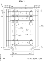
- FIG. 2 is a schematic plan view of a display device according to an embodiment.
- FIG. 3 is a schematic block diagram of a display device according to an embodiment.
- the display panel 100 may include sub-pixels SP, and scan lines SL, emission lines EM, and data lines DL, and a first driving voltage line VDDL electrically connected to the sub-pixels SP.
- the before mentioned pixels each may be comprised of several sub-pixels SP. Each of the sub-pixels SP has to be supplied by a voltage via different electrical lines. Thus, the before mentioned pixels may be also termed as sub-pixels or the sub-pixels may be termed as pixels. This applies to the whole disclosure of the present description and claims.
- the scan lines SL and the emission lines EM may extend in the first direction X
- the data lines DL and the first driving voltage line VDDL may extend in the second direction Y intersecting the first direction X.
- the first driving voltage line VDDL may extend in the second direction Y in the display area DA.
- the first driving voltage lines VDDL may be electrically connected to each other in the non-display area NDA.
- Each of the sub-pixels SP may be electrically connected to at least one of the scan lines SL, at least one of the data lines DL, at least one of the emission lines EM, and the first driving voltage line VDDL.
- FIG. 2 it is illustrated that each of the sub-pixels SP is electrically connected to four scan lines SL, a data line DL, an emission line EM, and the first driving voltage line VDDL, but the embodiments are not limited thereto.
- each of the sub-pixels SP may be electrically connected to three or fewer scan lines SL instead of four scan lines SL, or may be electrically connected to five or more scan lines SL.
- Each of the sub-pixels SP may include a driving transistor, at least one transistor, a light emitting element, and a capacitor.
- the driving transistor and the at least one transistor may be thin-film transistors.
- the at least one transistor may be turned on or off according to a scan signal applied from a scan line to act as a switching element. For example, in case that a transistor disposed between the data line and the gate electrode of the driving transistor is turned on by a scan signal, the data voltage of the data line may be applied to the gate electrode of the driving transistor.
- the light emitting element may be an organic light emitting diode including a first electrode, an organic light emitting layer, and a second electrode. The light emitting element may emit light according to the driving current of the driving transistor.
- the capacitor may serve to keep constant the data voltage applied to the gate electrode of the driving transistor.
- the display driving circuit 200 may include a timing controller 210, a data driver 220, and voltage lines.
- the timing controller 210 may receive digital video data DATA and timing signals from the circuit board 300.
- the timing controller 210 may generate scan control signals SCS1, SCS2, SCS3, and SCS4 for controlling an operation timing of each of scan drivers 410, 420, 430, and 440 according to the timing signals, may generate an emission control signal ECS for controlling an operation timing of an emission control driver 450, and may generate a data control signal DCS for controlling an operation timing of the data driver 220.
- the timing controller 210 may generate the first scan control signal SCS1, the second scan control signal SCS2, the third scan control signal SCS3, and the fourth scan control signal SCS4 according to the timing signals, may output the first scan control signal SCS1 to the first scan driver 410, may output the second scan control signal SCS2 to the second scan driver 420, may output the third scan control signal SCS3 to the third scan driver 430, and may output the fourth scan control signal SCS4 to the fourth scan driver 440.
- the timing controller 210 may output the scan control signals SCS1, SCS2, SCS3, and SCS4 to the scan drivers 410, 420, 430, and 440, respectively, through scan control lines SCL, and may output the emission control signal ECS to the emission control driver 450.
- the timing controller 210 may output the digital video data DATA and the data control signal DCS to the data driver 220.
- the data driver 220 may convert the digital video data DATA into analog data voltages to output the analog data voltages to the data lines DL through fan-out lines FL.
- Each of the voltage lines may be supplied with a voltage from a power supply unit (or power supply, not shown).
- the voltage lines may include the first driving voltage line VDDL for applying a first driving voltage Vdd, a first high-voltage line VGHL for applying a first high voltage VGH1, a first low-voltage line VGLL for applying a first low voltage VGL1, a second high-voltage line VGHO for applying a second high voltage VGH2, and a second low-voltage line VGLO for applying a second low voltage VGL2.
- Each of the first high-voltage line VGHL, the first low-voltage line VGLL, the second high-voltage line VGHO, and the second high-voltage line VGHO will be described in detail with reference to FIG. 4 .
- the voltage lines may further include a second driving voltage line VSSL (see FIG. 6 ) supplying a second driving voltage to the cathode electrode of the organic light emitting diode of each of the sub-pixels SP, and a bias voltage line VEHL (see FIG. 6 ) supplying a bias voltage to the source electrode of the driving transistor of each of the sub-pixels SP.
- VSSL second driving voltage line
- VEHL bias voltage line
- the first driving voltage may be a high-potential voltage for driving the organic light emitting diode
- the second driving voltage may be a low-potential voltage for driving the organic light emitting diode.
- the first driving voltage may have a higher potential than the second driving voltage.
- the bias voltage may be a voltage for setting an operating point of the driving transistor in case that the frequency is varied, and may be a voltage that may be optionally set. According to an embodiment, the bias voltage may have a potential greater than the first driving voltage, but is not limited thereto. For example, the bias voltage may have a potential smaller than the first driving voltage.
- a scan driving circuit 400 for applying scan signals to the scan lines SL, the fan-out lines FL between the data lines DL and the display driving circuit 200, and the pads DP electrically connected to the display driving circuit 200 may be disposed.
- the display driving circuit 200 and the pads DP may be disposed adjacent to an edge of a side (e.g., a lower side) of the display panel 100.
- the scan driving circuit 400 may be electrically connected to the display driving circuit 200 through scan control lines SCL.
- the scan driving circuit 400 may receive the scan control signals SCS1, SCS2, SCS3, and SCS4 and the emission control signal ECS from the display driving circuit 200 through the scan control lines SCL.
- the scan driving circuit 400 may generate scan signals respectively according to the scan control signals SCS and may sequentially output the scan signals to the scan lines SL.
- the emission control driver 450 may generate emission signals according to the emission control signal ECS and may sequentially output the emission signals to the emission lines EM.
- the scan driving circuit 400 may include thin-film transistors.
- the scan driving circuit 400 and the thin-film transistors of the sub-pixels SP may be formed on the same layer.
- the scan driving circuit 400 may be disposed in the non-display area NDA on both sides (for example, left and right sides) of the display area DA. Through such a structure, it may be advantageous in reducing the length of the non-display area NDA in the first direction X on each of both sides of the display area DA.
- the embodiments are not limited thereto.
- the scan driving circuit 400 may be disposed on either the left side or the right side of the display area DA.
- the scan driving circuit 400 may include the first scan driver 410, the second scan driver 420, the third scan driver 430, the fourth scan driver 440, and the emission control driver 450.
- FIGS. 2 and 3 illustrate that the second scan driver 420 includes a first sub-scan driver 421 disposed on a side of the non-display area NDA, for example, on the left side of the non-display area NDA, and a second sub-scan driver 422 disposed on another side of the non-display area NDA, for example, on the right side of the non-display area NDA, and that each of the first sub-scan driver 421 and the second sub-scan driver 422 applies a scan signal, but the disclosure is not limited thereto.
- the scan driving circuit 400 may include one second scan driver 420 and may be disposed on either one side or another side of the non-display area DA.
- the first scan driver 410 and the third scan driver 430 may be disposed on different sides of the non-display area NDA.
- the third scan driver 430 may be disposed on another side of the non-display area NDA, and conversely, in case that the first scan driver 410 is disposed on another side of the non-display area NDA, the third scan driver 430 may be disposed on a side of the non-display area NDA.
- the fourth scan driver 440 and the emission control driver 450 may be disposed on different sides of the non-display area NDA.
- the fourth scan driver 440 in case that the emission control driver 450 is disposed on a side of the non-display area NDA, the fourth scan driver 440 is disposed on another side of the non-display area NDA, and conversely, in case that the emission control driver 450 is disposed on another side of the non-display area NDA, the fourth scan driver 440 may be disposed on a side of the non-display area NDA.
- At least two voltage lines of the voltage lines VGHL, VGLL, VGHO, and VGLO for applying a voltage to the scan lines SL may be electrically connected to each of the scan drivers 410, 420, 430, and 440.
- the voltage lines VGHO and VGLL for applying a voltage to the emission lines EM may be electrically connected to the emission control driver 450.
- the transistors of each of the sub-pixels SP include at least one N-channel transistor and at least one P-channel transistor
- scan signals to be applied to the respective gate electrodes of the N-channel transistor and the P-channel transistor may be different. Accordingly, the scan lines electrically connected to the respective gate electrodes of the N-channel transistor and the P-channel transistor should be divided, and accordingly, the scan driver may be divided.
- the first scan driver 410 and the third scan driver 430 may be scan drivers for applying a scan signal to the N-channel transistor
- the second scan driver 420, the fourth scan driver 440, and the emission control driver 450 may be drivers for applying a scan signal to the P-channel transistor.
- the second high-voltage line VGHO and the second low-voltage line VGLO may be electrically connected to the first scan driver 410 and the third scan driver 430, respectively.
- the first high-voltage line VGHL and the first low-voltage line VGLL may be electrically connected to the second scan driver 420 and the fourth scan driver 440, respectively.
- Each of the first low-voltage line VGLL and the second high-voltage line VGHO may be electrically connected to the emission control driver 450.
- the first high voltage VGH1 applied from the first high-voltage line VGHL may be a first gate-off voltage Voff1 for turning off the P-channel transistor
- the first low voltage VGL1 applied from the first low-voltage line VGLL may be a first gate-on voltage Von1 for turning on the P-channel transistor.
- the first high voltage VGH1 may be used to turn on the N-channel transistor
- the first low voltage VGL1 may be used to turn off the N-channel transistor.
- the second high voltage VGH2 applied from the second high-voltage line VGHO may be a second gate-on voltage Von2 for turning on the N-channel transistor
- the second low voltage VGL2 applied from the second low-voltage line VGLO may be a second gate-off voltage Voff2 for turning off the N-channel transistor.
- the second high voltage VGH2 may be used to turn off the P-channel transistor
- the second low voltage VGL2 may be used to turn on the P-channel transistor.
- the magnitude of the first high voltage VGH1 and the magnitude of the second high voltage VGH2 may be substantially the same, and the magnitude of the first low voltage VGL1 and the magnitude of the second low voltage VGL2 may be substantially the same, but the disclosure is not limited thereto.
- the magnitude of the first high voltage VGH1 and the magnitude of the second high voltage VGH2 may be different, and the magnitude of the first low voltage VGL1 and the magnitude of the second low voltage VGL2 may be different.
- the scan lines SL and the data lines DL intersect each other in the display area DA, and a first parasitic capacitor Cpr1 may be formed in each gap between the scan lines SL and the data lines DL that intersect each other as illustrated in FIG. 3 . Accordingly, scan signals being outputted from the scan lines SL may be coupled (or connected) according to the data signal outputted from the data line DL.
- Voltage fluctuations due to the coupling between the data line DL and the scan lines SL may affect the voltage of each of the voltage lines VGLL, VGHL, VGLO, and VGHO according to the voltage being outputted from each of the scan drivers 410, 420, 430, and 440.
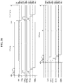
- the period having the first low voltage VGL1 is shorter than the period having the first high voltage VGH1
- voltage fluctuations due to coupling between the data line DL and second scan lines GW may occur in the first high-voltage line VGHL.
- the voltage of the first low-voltage line VGLL may be maintained substantially constant at the first low voltage VGL1.
- the first low voltage line VGLL may be relatively stable from voltage fluctuations according to the data signal compared to the first high-voltage line VGHL.
- the period having the second high voltage VGH2 is shorter than the period having the second low voltage VGL2
- voltage fluctuations due to coupling between the data line DL and first scan lines GI may occur in the second low-voltage line VGLO.
- the voltage of the second high-voltage line VGHO may be maintained substantially constant at the second high voltage VGH2.
- the second high voltage line VGHO may be relatively stable from voltage fluctuations according to the data signal compared to the second low-voltage line VGLO.
- the emission control driver 450 since the emission signal outputted from the emission control driver 450 may have the first low voltage VGL1 applied from the first low-voltage line VGLL or the second high voltage VGH2 applied from the second high-voltage line VGHO, it may be advantageous in reducing voltage fluctuations due to the data signal of the data line DL.
- FIG. 4 is a schematic block diagram according to an example of stages of a second scan driver of FIG. 3 .
- the second scan driver 420 may include the stages STAW that are dependently electrically connected.
- the number of stages STAW of the second scan driver 420 may be the same as the number of second scan lines GW.
- the stages STAW of the second scan driver 420 may output a second scan signal.
- the n th (n is a positive integer) stage STAWn of the second scan driver 420 may be electrically connected to a second scan line GWn electrically connected to each of the sub-pixels SP in an n th row and may output a second scan signal.
- the (n+1) th stage STAWn+1 of the second scan driver 420 may be electrically connected to a second scan line GWn+1 electrically connected to each of the sub-pixels SP in an (n+1) th row and may output a second scan signal.
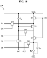
- Each of the stages STAWn and STAWn+1 of the second scan driver 420 may include, as illustrated in FIG. 4 , a pull-up node NQ, a pull-down node NQB, a pull-up transistor TU that is turned on in case that the pull-up node NQ has a gate-on voltage, a pull-down transistor TD that is turned on in case that the pull-down node NQB has a gate-on voltage, a node controller NC for controlling the charging and discharging of the pull-up node NQ and the pull-down node NQB, and an output terminal OT.
- the output terminal OT may be electrically connected to any of the second scan lines GW.
- the stages STAW may be sequentially electrically connected to the second scan lines GW.
- the output terminal OT of the n th stage STAWn may be electrically connected to the second scan line GWn of an n th row
- the output terminal OT of the (n+1) th stage STAWn+1 may be electrically connected to the second scan line GWn+1 of an (n+1) th row.
- the node controller NC may include thin-film transistors, a start terminal ST, a reset terminal RT, a gate-on voltage terminal VGLT, a gate-off voltage terminal VGHT, and a clock terminal CT.
- the start terminal ST may be electrically connected to a front-end carry line PCL to which an output signal of a front-end stage is applied.
- the reset terminal RT may be electrically connected to a rear-end carry line RCL to which an output signal of a rear-end stage is inputted.
- the gate-on voltage terminal VGLT may be electrically connected to the first low-voltage line VGLL for applying the first low voltage VGL1.
- the gate-off voltage terminal VGHT may be electrically connected to the first high-voltage line VGHL for applying the first high voltage VGH1.
- the first low voltage VGL1 may be the first gate-on voltage Von1 for turning on the P-channel transistor
- the first high voltage VGH1 may be the first gate-off voltage Voff1 for turning off the P-channel transistor.
- the clock terminal CT may be electrically connected to one of a first clock line CL1 to which the first clock signal is applied and a second clock line CL2 to which the second clock signal is applied.
- the stages STAW may be alternately connected to the first clock line CL1 and the second clock line CL2.
- the clock terminal CT of the n th stage STAWn is electrically connected to the first clock line CL1
- the clock terminal CT of the (n+1) th stage STAWn+1 may be electrically connected to the second clock line CL2.
- FIG. 4 illustrates that the stages STAWn and STAWn+1 are alternately electrically connected to the two clock lines CL1 and CL2, but the disclosure is not limited thereto.
- the stages STAWn and STAWn+1 may be alternately electrically connected to three or more clock lines.
- the node controller NC may control the charging and discharging of the pull-up node NQ and the pull-down node NQB according to an output signal of the front-end stage inputted to the start terminal ST. In order to stably control the output of the stage, the node controller NC may cause the pull-down node NQB to have a gate-off voltage in case that the pull-up node NQ has a gate-on voltage, and cause the pull-up node NQ to have a gate-off voltage in case that the pull-down node NQB has a gate-on voltage. To this end, the node controller NC may include thin-film transistors.
- the pull-up transistor TU may be turned on in case that the pull-up node NQ has a gate-on voltage, and may output any of clock signals inputted to the clock terminal CT to the output terminal OT.
- the pull-down transistor TD may be turned on in case that the pull-down node NQB has a gate-on voltage, and may output the voltage of the gate-off voltage terminal to the output terminal OT.
- Each of the stages STAWn and STAWn+1 may further include a first capacitor C1 disposed between the pull-up node NQ and the output terminal OT.
- the first capacitor C1 may maintain a potential difference between the gate electrode of the pull-up transistor TU and the output terminal OT during a period in which the pull-up transistor TU is turned on.
- FIG. 4 illustrates that each of the stages STAW of the second scan driver 420 outputs a second scan signal to a second scan line GW, but the disclosure is not limited thereto.
- each of the stages STAW of the second scan driver 420 may include two or more node controllers NC, similar to stages STAE of the emission control driver 450 of FIG. 5 to be described below, and may output the second scan signals to each of two or more second scan lines GW.
- each of the second scan lines GW intersects the data line DL in the display area DA, and the first parasitic capacitor Cpr1 may be formed between the second scan line GW and the data line DL that intersect each other. Accordingly, in case that the data signal of the data line DL fluctuates, the voltage being outputted to the second scan line GW may fluctuate.
- the voltage of the first high-voltage line VGHL for applying the first high voltage VGH1 due to the coupling of the data line DL and the second scan line GWn of the n th row may also increase and then may be restored to the original voltage magnitude.
- the first low-voltage line VGLL is electrically connected to the n th stage STAWn of the second scan driver 420 but is in a short-circuited state, and thus there is no effect on the first low voltage VGL1 of the first low-voltage line VGLL.
- the voltage of the first high-voltage line VGHL for applying the first high voltage VGH1 due to the coupling of the data line DL and the second scan line GWn of the n th row may also decrease and be restored to the original voltage magnitude.
- FIG. 5 is a schematic block diagram according to an example of a stage of the emission control driver 450 of FIG. 3 .
- the stage STAE of the emission control driver 450 of FIG. 5 is different from the stage STAW of the second scan driver 420 of FIG. 4 at least in that two node controllers NC1 and NC2 are included, and gate-off voltage terminals VGHT1 and VGHT2 of each of the node controllers NC1 and NC2 are electrically connected to the second high-voltage line VGHO for applying the second high voltage VGH2. Differences from the stage STAW of the second scan driver 420 of FIG. 4 will be mainly described with reference to FIG. 6 .
- the number of stages STAE of the emission control driver 450 may be smaller than the number of emission lines EM.
- the number of stages STAE of the emission control driver 450 may be 1/2 of the number of emission lines EM.
- the stages STAE of the emission control driver 450 may sequentially output two emission signals.
- the k th (k is a positive integer) stage STAEk of the emission control driver 450 may be electrically connected to the emission line EMn electrically connected to each of the sub-pixels SP in the n th row and an emission line EMn+1 electrically connected to each of the sub-pixels SP of the (n+1) th row and may output emission signals.
- the first output terminal OT1 of the k th stage STAEk is electrically connected to the n th emission line EMn
- a second output terminal OT2 is electrically connected to the (n+1) th emission line EMn+1
- the first output terminal OT1 of a (k+1) th stage STAEk+1 may be electrically connected to an (n+2) th emission line EMn+2
- the second output terminal OT2 may be electrically connected to an (n+3) th emission line EMn+3.
- the first node controller NC1 and the second node controller NC2 of each of the stages STAE of the emission control driver 450 differ only in that each of the gate-off voltage terminals VGHT1 and VGHT2 is electrically connected to the second high-voltage line VGHO for applying the second high voltage VGH2, and may be substantially the same as the node controller NC of the stage STAW of the second scan driver 420 of FIG. 4 .
- first gate-on voltage terminal VGLT1 of the first node controller NC1 of each of the stages STAE of the emission control driver 450 is electrically connected to the first low-voltage line VGLL
- first gate-off voltage terminal VGHT1 is electrically connected to the second high-voltage line VGHO
- second gate-on voltage terminal VGLT2 of the second node controller NC2 is electrically connected to the first low-voltage line VGLL
- the second gate-off voltage terminal VGHT2 is electrically connected to the second high-voltage line VGHO
- FIG. 5 illustrates that each of the stages STAE of the emission control driver 450 includes two node controllers NC1 and NC2, but embodiments are not limited thereto.
- each of the stages STAE of the emission control driver 450 may include a node controller NC, and include two pull-up nodes NQ (e.g., NQ1 and NQ2), two pull-down nodes NQB, two pull-up transistors TU (e.g., TU1 and TU2), two pull-down transistors TD (e.g., TD1 and TD2), and two output terminals OT, or may include only a node controller NC, a pull-up node NQ, a pull-down node NQB (e.g., NQB1 and NQB2), a pull-up transistor TU, and a pull-down transistor TD, but include two output terminals OT.
- NQ e.g., NQ1 and NQ2
- TU e.g., TU1
- the stages STAE may include capacitors C2 and C3.
- the detailed circuit configuration of the node controller NC may be different from the detailed circuit configuration of the node controllers NC1 and NC2 of each of the stages STAE of the emission control driver 450 of FIG. 6 .
- the detailed circuit configuration may include a number and connection relationship of the thin-film transistors of each of the node controllers, a number of clock terminals CT (e.g., CT1) electrically connected to clock lines (e.g., CL3 and CL4), a number of start terminals ST and reset terminals RT, and the like.
- FIG. 5 illustrates that each of the stages STAE of the emission control driver 450 is electrically connected to two emission lines EM, but each of the stages STAE of the emission control driver 450 may be electrically connected to an emission line EM or three or more emission lines EM.
- the stages of each of the first scan driver 410 and the third scan driver 430 differ only in that the gate-on voltage terminal of the node controller is electrically connected to the second high-voltage line VGHO and the gate-off voltage terminal is electrically connected to the second low-voltage line VGLO, and may be substantially the same as the stages of the emission control driver 450 of FIG. 6 .
- the stages of the fourth scan driver 440 differ only in that the gate-off voltage terminal of the node controller is electrically connected to the first high-voltage line VGHL, and may be substantially the same as the stages of the emission control driver 450 of FIG. 6 .
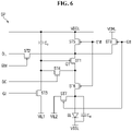
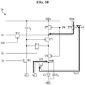
- FIG. 6 is a schematic circuit diagram according to an example of the sub-pixel SP.
- Each of the sub-pixels SP may be electrically connected to the first scan line GI, the second scan line GW, a third scan line GC, a fourth scan line GB, the emission line EM, and the data line DL.
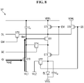
- Each of the sub-pixels SP may be electrically connected to the first driving voltage line VDDL supplied with a first driving voltage, the second driving voltage line VSSL supplied with a second driving voltage, the bias voltage line VEHL supplied with a bias voltage, a first initialization voltage line VIL1 supplied with a first initialization voltage Vint1 (see FIG. 8 ), and a second initialization voltage line VIL2 supplied with a second initialization voltage Vint2 (see FIG. 10 ).
- Each of the sub-pixels SP may include first to eighth transistors ST1 to ST8, a light emitting element EL, and at least one capacitor.
- the first transistor ST1 may be a driving transistor
- the second to eighth transistors ST2 to ST8 may be transistors that function as switch elements that are turned on or off according to a scan signal applied to each of the gate electrodes.
- the numeration of transistors in the FIGs. is different to that from the claims and the above general part of the description.
- the fifth transistor of the claims may correspond to the fourth transistor ST4 in the FIGs.
- the sixth transistor in the claims may correspond to the seventh transistor ST7 in the Figs.
- the third transistor in a claim may correspond to the seventh transistor ST7 in the FIGs.
- the numeration of the different electrical lines may vary between the Figs. and the claims or between different embodiments defined in the claims.
- the first transistor ST1 may include a gate electrode, a first electrode, and a second electrode.
- the gate electrode may be a gate electrode disposed on an active layer of the first transistor ST1.
- the first transistor ST1 may control a source-drain current Isd (hereinafter referred to as "driving current”) according to the data voltage applied to the gate electrode.
- the driving current Isd flowing through the channel of the first transistor ST1 is proportional to the square of the difference between the voltage between the source electrode and the gate electrode of the first transistor ST1 and the absolute value of a threshold voltage Vth, as shown in Equation 1.
- Isd k ′ ⁇ Vsg ⁇ Vth 2
- Equation 1 k' represents a proportionality coefficient determined by the structure and physical characteristics of the first transistor ST1
- Vsg represents the source-gate voltage of the first transistor ST1
- Vth represents the threshold voltage of the first transistor ST1.
- the light emitting element EL may emit light by the driving current Isd.
- the amount of light emitted from the light emitting element EL may be proportional to the magnitude of the driving current Isd.
- the light emitting element EL may be an organic light emitting diode including an anode electrode, a cathode electrode, and an organic light emitting layer disposed between the anode electrode and the cathode electrode.
- the light emitting element EL may be an inorganic light emitting diode including an anode electrode, a cathode electrode, and an inorganic light emitting layer disposed between the anode electrode and the cathode electrode.
- the light emitting element EL may be a quantum dot light emitting element including an anode electrode, a cathode electrode, and a quantum dot light emitting layer disposed between the anode electrode and the cathode electrode.
- the light emitting element EL may be a micro light emitting diode.
- the anode electrode of the light emitting element EL may be electrically connected to a second electrode of the sixth transistor ST6 and a second electrode of the seventh transistor ST7, and the cathode electrode may be electrically connected to the second driving voltage line VSSL.
- a parasitic capacitance Cel may be formed between the anode electrode and the cathode electrode of the light emitting element EL.
- the second transistor ST2 may be disposed between the data line DL and the first electrode of the first transistor ST1.
- the second transistor ST2 may be turned on by the scan signal of the second scan line GW to electrically connect the first electrode of the first transistor ST1 to the data line DL.
- a gate electrode of the second transistor ST2 may be electrically connected to the second scan line GW, a first electrode thereof may be electrically connected to the data line DL, and a second electrode thereof may be electrically connected to the first electrode of the first transistor ST1.
- the third transistor ST3 may be disposed between the first initialization voltage line VIL1 and the gate electrode of the first transistor ST1.
- the third transistor ST3 may be turned on by the scan signal of the first scan line GI to electrically connect the gate electrode of the first transistor ST1 to the first initialization voltage line VIL1.
- the gate electrode of the first transistor ST1 may be discharged to the first initialization voltage Vint1 of the first initialization voltage line VIL1.
- a gate electrode of the third transistor ST3 may be electrically connected to the first scan line GI, a first electrode thereof may be electrically connected to the gate electrode of the first transistor ST1, and a second electrode thereof may be electrically connected to the first initialization voltage line VIL1.
- the fourth transistor ST4 may be disposed between the gate electrode of the first transistor ST1 and the second electrode of the first transistor ST1.
- the fourth transistor ST4 may be turned on by the scan signal of the third scan line GC to electrically connect the gate electrode of the first transistor ST1 to the second electrode.
- the first transistor ST1 may be driven as a diode.
- a gate electrode of the fourth transistor ST4 may be electrically connected to the third scan line GC, a first electrode thereof may be electrically connected to the gate electrode of the first transistor ST1, and a second electrode thereof may be electrically connected to the second electrode of the first transistor ST1.
- the fifth transistor ST5 may be disposed between the first driving voltage line VDDL and the first electrode of the first transistor ST1.
- the fifth transistor ST5 may be turned on by the emission signal of the emission line EM to electrically connect the first electrode of the first transistor ST1 to the first driving voltage line VDDL.
- a gate electrode of the fifth transistor ST5 may be electrically connected to the emission line EM, a first electrode thereof may be electrically connected to the first driving voltage line VDDL, and a second electrode thereof may be electrically connected to the first electrode of the first transistor ST1.
- the sixth transistor ST6 may be disposed between the second electrode of the first transistor ST1 and the anode electrode of the light emitting element EL.
- the sixth transistor ST6 may be turned on by the emission signal of the emission line EM to electrically connect the second electrode of the first transistor ST1 to the anode electrode of the light emitting element EL.
- the gate electrode of the sixth transistor ST6 may be electrically connected to the emission line EM, a first electrode thereof may be electrically connected to the second electrode of the first transistor ST1, and the second electrode thereof may be electrically connected to the anode electrode of the light emitting element EL.
- the driving current Isd may be supplied to the light emitting element EL.
- the seventh transistor ST7 may be disposed between the second initialization voltage line VIL2 and the anode electrode of the light emitting element EL.
- the seventh transistor ST7 may be turned on by the scan signal of the fourth scan line GB to electrically connect the second initialization voltage line VIL2 to the anode electrode of the light emitting element EL.
- the anode electrode of the light emitting element EL may be discharged with the second initialization voltage Vint2.
- a gate electrode of the seventh transistor ST7 may be electrically connected to the fourth scan line GB, a first electrode thereof may be electrically connected to the second initialization voltage line VIL2, and the second electrode thereof may be electrically connected to the anode electrode of the light emitting element EL.
- the eighth transistor ST8 may be disposed between the bias voltage line VEHL and the first electrode of the first transistor ST1.
- the eighth transistor ST8 may be turned on by the scan signal of the fourth scan line GB to electrically connect the bias voltage line VEHL to the first electrode of the first transistor ST1.
- a gate electrode of the eighth transistor ST8 may be electrically connected to the fourth scan line GB, a first electrode thereof may be electrically connected to the bias voltage line VEHL, and a second electrode thereof may be electrically connected to the first electrode of the first transistor ST1.
- the storage capacitor Cst may be formed between the gate electrode of the first transistor ST1 and the first driving voltage line VDDL.
- An electrode of the storage capacitor Cst may be electrically connected to the gate electrode of the first transistor ST1, and another electrode thereof may be electrically connected to the first driving voltage line VDDL. Accordingly, the storage capacitor Cst may maintain a potential difference between the gate electrode of the first transistor ST1 and the first driving voltage line VDDL.
- the second electrode may be a drain electrode.
- the second electrode may be a source electrode.
- the active layer of each of the first to eighth transistors ST1 to ST8 may be formed of any of polysilicon, amorphous silicon, and an oxide semiconductor.
- the first transistor ST1, the second transistor ST2, and the fifth to eighth transistors ST5, ST6, ST7, and ST8 may be P-channel transistors
- the third transistor ST3 and the fourth transistor ST4 may be N-channel transistors
- the active layer of each of the first transistor ST1, the second transistor ST2, and the fifth to eighth transistors ST5, ST6, ST7, and ST8 formed of P-channel transistors may be formed of polysilicon
- the active layer of each of the third transistor ST3 and the fourth transistor ST4 formed of N-channel transistors may be formed of an oxide.
- the active layer of each of the third transistor ST3 and the fourth transistor ST4 electrically connected to the gate electrode of the first transistor ST1 may be formed as N-channel transistors, which are oxides, so that it may be advantageous in decreasing a leakage current and reducing power consumption.
- FIG. 7 is a waveform diagram of signals applied to each of a first scan line, a second scan line, a third scan line, a fourth scan line, and an emission line electrically connected to the sub-pixel of FIG. 6 .
- a first scan signal SGI is a signal applied to the first scan line GI and is a signal for controlling turn-on and turn-off of the third transistor ST3.
- a second scan signal SGW is a signal applied to the second scan line GW and is a signal for controlling turn-on and turn-off of the second transistor ST2.
- a third scan signal SGC is a signal applied to the third scan line GC and is a signal for controlling turn-on and turn-off of the fourth transistor ST4.
- a fourth scan signal SGB is a signal applied to the fourth scan line GB and is a signal for controlling turn-on and turn-off of each of the seventh transistor ST7 and the eighth transistor ST8.
- An emission signal SEM is a signal applied to the emission line EM and is a signal for controlling turn-on and turn-off of each of the fifth transistor ST5 and the sixth transistor ST6.
- the emission control driver 450 uses the first low-voltage line VGLL electrically connected to the second scan driver 420 and the second high-voltage line VGHO electrically connected to the first scan driver 410 in generating the emission signal SEM for controlling the fifth transistor ST5 and the sixth transistor ST6, and thus the emission signal SEM may have the first gate-on voltage Von1 that is the first low voltage VGL1, and the second gate-on voltage Von2 that is the second high voltage VGH2.
- each of the fifth transistor ST5 and the sixth transistor ST6 is turned on, and in case that the emission signal SEM has the second gate-on voltage Von2 that is the second high voltage VGH2, each of the fifth transistor ST5 and the sixth transistor ST6 is turned off.
- the first to fourth scan signals SGI, SGW, SGC, and SGB and the emission signal SEM may be generated at a cycle of a frame period.
- a frame period may be divided into a first period t1, a second period t2, a third period t3, and a fourth period t4.
- the first period t1 is a period in which the voltage of the gate electrode of the first transistor ST1 is initialized to the first initialization voltage Vint1 by applying the first initialization voltage Vint1 to the gate electrode of the first transistor ST1.
- the second period t2 is a period in which the data voltage is supplied to the first electrode of the first transistor ST1 and the threshold voltage Vth of the first transistor ST1 is sampled.
- the third period t3 is a period in which the voltage of the anode electrode of the light emitting element EL is initialized to the second initialization voltage Vint2 by applying the second initialization voltage Vint2 to the anode electrode of the light emitting element EL.
- the driving frequency changes, it may be a period in which a bias voltage is applied to the first electrode of the first transistor ST1 to artificially set the bias voltage of the first transistor ST1.
- the fourth period t4 is a period in which the driving current Isd flowing according to the voltage of the gate electrode of the first transistor ST1 is supplied to the light emitting element EL and the light emitting element EL emits light.
- the first scan signal SGI may have the second gate-on voltage Von2 during the first period t1 and may have the second gate-off voltage Voff2 during the remaining periods t2, t3, and t4.
- the second scan signal SGW may have the first gate-on voltage Von1 in the second period t2 and may have the first gate-off voltage Voff1 during the remaining periods t1, t3, and t4.
- the third scan signal SGC may have the second gate-on voltage Von2 in the second period t2 and may have the second gate-off voltage Voff2 during the remaining periods t1, t3, and t4.
- the fourth scan signal SGB may have the first gate-on voltage Von1 in the third period t3 and may have the first gate-off voltage Voff1 during the remaining periods t1, t2, and t4.
- the emission signal SEM may have the first gate-on voltage Von1 in the fourth period t4 and may have the second gate-on voltage Von2 during the remaining periods t1, t2, and t3.
- the fourth period t4 may also include first sub-periods in which the emission signal SEM has the second gate-on voltage Von2 and second sub-periods in which the emission signal SEM has the first gate-on voltage Von1.
- the first sub-periods and the second sub-periods may be alternately disposed.
- FIG. 7 illustrates that a period in which the first scan signal SGI has the second gate-on voltage Von2 is substantially the same as the first period t1, but the period in which the first scan signal SGI has the second gate-on voltage Von2 may be shorter than the first period t1.
- FIG. 7 illustrates that a period in which the second scan signal SGW has the first gate-on voltage Von1 is shorter than the second period t2 and a period in which the fourth scan signal SGB has the first gate-on voltage Von1 is shorter than the third period t3, but the period in which the second scan signal SGW has the first gate-on voltage Von1 may be substantially the same as the second period t2, and the period in which the fourth scan signal SGB has the first gate-on voltage Von1 may be substantially the same as the third period t3.
- a period in which a third scan signal SGC has the second gate-on voltage Von2 may be shorter than the second period t2 as illustrated in FIG. 7 , but the disclosure is not limited thereto.
- a period in which the third scan signal SGC has the second gate-on voltage Von2 may be substantially the same as the second period t2, and the period in which the third scan signal SGC has the second gate-on voltage Von2 may at least partially overlap the period in which the first scan signal SGI has the second gate-on voltage Von2, and may have the second gate-on voltage Von2 in the first period t1.
- FIG. 7 illustrates that each of the first period t1 and the second period t2 is a horizontal period.
- a horizontal period indicates a period in which the data voltage is supplied to each of the sub-pixels SP electrically connected to any scan line of the display panel 100, and thus may be defined as a horizontal line scan period.
- the data voltages may be supplied to the data lines DL in synchronization with the gate-on voltage of each of the scan signals.
- FIGS. 8 to 11 are schematic circuit diagrams illustrating a method of driving the sub-pixel of FIG. 6 during the first to fourth periods of FIG. 7 .
- the first scan signal SGI having the second gate-on voltage Von2 is supplied to the first scan line GI.
- the third transistor ST3 is turned on by the first scan signal SGI. Because of the turn-on of the third transistor ST3, the gate electrode of the first transistor ST1 is initialized to the first initialization voltage Vint1 of the first initialization voltage line VIL1.
- the second scan signal SGW having the first gate-on voltage Von1 is supplied to the second scan line GW. Accordingly, the second transistor ST2 electrically connected to the second scan line GW is turned on to supply a data voltage Vdata to the first electrode of the first transistor ST1.
- the third scan signal SGC having the second gate-on voltage Von2 is supplied to the third scan line GC, so that the fourth transistor ST4 is turned on. Because of the turn-on of the fourth transistor ST4, the gate electrode and the second electrode of the first transistor ST1 are electrically connected, and the first transistor ST1 is driven as a diode.
- the first transistor ST1 forms a current path until the voltage Vsg between the gate electrode and the source electrode reaches the absolute value of the threshold voltage Vth. Accordingly, the voltage of the gate electrode and the second electrode of the first transistor ST1 rises up to the difference voltage (Vdata -
- ) may be stored in the storage capacitor Cst.
- the driving current Isd of the first transistor ST1 may be proportional to a voltage Vsd between the source electrode and the drain electrode of the first transistor ST1 in a section in which the voltage Vsd between the source electrode and the drain electrode of the first transistor ST1 is greater than 0V.
- the threshold voltage Vth of the first transistor ST1 may be less than 0V.
- the fourth scan signal SGB having the first gate-on voltage Von1 is supplied to the fourth scan line GB.
- the seventh transistor ST7 is turned on by the fourth scan signal SGB, so that the anode electrode of the light emitting element EL is initialized to the second initialization voltage Vint2 of the second initialization voltage line VIL2.
- the eighth transistor ST8 may be turned on by the fourth scan signal SGB to supply a bias voltage to the first electrode of the first transistor ST1. Accordingly, an operating point of the first transistor ST1 may be set in advance. For example, since the magnitude of the driving current Isd for the light emitting element EL to emit light may be different according to the frequency, in case that the frequency is changed, by applying a bias voltage, which is higher than the first driving voltage, to the first electrode of the first transistor ST1 in advance to set an operating point, it may be advantageous in reducing a phenomenon in which the light emitting element EL flickers according to a frequency change.
- the emission signal SEM having the first gate-on voltage Von1 is supplied to the emission line EM.
- each of the fifth transistor ST5 and the sixth transistor ST6 is turned on by the emission signal SEM.
- the first electrode of the first transistor ST1 is electrically connected to the first driving voltage line VDDL because of the turn-on of the fifth transistor ST5, and the second electrode of the first transistor ST1 is electrically connected to the anode electrode of the light emitting element EL because of the turn-on of the sixth transistor ST6.
- the driving current Isd flowing according to the voltage of the gate electrode of the first transistor ST1 may be supplied to the light emitting element EL.
- Equation 2 k' represents a proportional coefficient determined by the structure and physical characteristics of the first transistor ST1
- Vth represents the threshold voltage of the first transistor ST1
- ELVDD represents the first driving voltage of the first driving voltage line VDDL
- Vdata represents the data voltage.
- the gate voltage of the first transistor ST1 is "Vdata -
- the driving current Isd does not depend on the threshold voltage Vth of the first transistor ST1.
- the threshold voltage Vth of the first transistor ST1 that is the driving transistor is compensated for.
- FIG. 12 is a schematic circuit diagram illustrating a second parasitic capacitor formed between an emission line of a sub-pixel and a gate electrode of a first transistor.
- FIG. 13 is a schematic view illustrating a test screen for checking whether horizontal crosstalk is generated according to a voltage change of a gate electrode of a first transistor.
- FIG. 14 is a schematic diagram illustrating horizontal crosstalk generated according to a voltage change of a gate electrode of a first transistor.
- FIG. 15 is a timing diagram illustrating an example of a voltage change of a gate electrode of a first transistor that may be generated by a second parasitic capacitor.
- a second parasitic capacitor Cpr2 may be formed between the gate electrode of the first transistor ST1 of the sub-pixel SP and the emission line EM as illustrated in FIG. 12 . Accordingly, in case that the voltage of the emission line EM changes, the voltage of the gate electrode of the first transistor ST1 may be affected.
- FIG. 15 illustrates only a part of the first period t1 and the second period t2 among the first to fourth periods t1 to t4 of FIG. 8 are illustrated.
- the second period t2 may include a first sub-period t21 in which the data signal SDL is changed, a second sub-period t22 in which the second scan line GW has the first gate-on voltage Von1, and a third sub-period t23 in which a second scan signal SGWg has the first gate-off signal Voff1.
- SGWg indicates a second scan signal applied to the second scan line GW disposed in the g th row
- SEMg indicates an emission signal applied to the emission line EM disposed in the g th row
- V G1 indicates the voltage of the gate electrode G1 of the first transistor ST1.
- a voltage change of the gate electrode of the first transistor ST1 which may occur in case that the first high-voltage line VGHL is electrically connected to the emission control driver 450 instead of the second high-voltage line VGHO as shown in FIG. 3 , and the emission control driver 450, the second scan driver 420, and the fourth scan driver 440 share the first high-voltage line VGHL, will be described in detail.
- the voltage of the second scan signal SGWg of the second scan line GW may be coupled to the data voltage by the first parasitic capacitor Cpr1 in FIG. 4 formed between the data line DL and the second scan line GW to rise by a first voltage difference ⁇ V1.
- the emission signal SEMg of the emission line EM that has been outputting the first high voltage VGH1 may also increase by a second voltage difference ⁇ V2 according to an increase in the potential of the first high-voltage line VGHL.
- a period in which the emission signal SEMg of the emission line EM increases by the second voltage difference ⁇ V2 and then recovers to the first high voltage VGH1 may continue until the second sub-period t22.
- a data voltage may be applied to the first electrode of the first transistor ST1 during the second sub-period t22 in which the second scan signal SGWg has the first gate-on voltage Von1, and the second electrode of the first transistor ST1 and the gate electrode thereof may be electrically connected so that the threshold voltage Vth of the first transistor ST1 may be compensated for.
- the voltage of the gate electrode of the first transistor ST1 may be coupled to the emission signal SEMg of the emission line EM by the second parasitic capacitor Cpr2 between the emission line EM and the gate electrode of the first transistor ST1.
- a voltage fluctuation ⁇ V3 of the emission signal SEMg during the third sub-period t23 may be reflected on a gate electrode G1 of the first transistor ST1 by the second parasitic capacitor Cpr2.
- the voltage of the gate electrode G1 of the first transistor ST1 may be lowered by a fourth voltage difference ⁇ V4.
- the voltage of the gate electrode G1 of the first transistor ST1 may be "Vdata -
- a black image B, a gray image G, and the black image B are sequentially displayed in the first direction X in a central area of the display panel 100, and the gray image G is displayed in the remaining areas
- a data voltage e.g., a black voltage Vbl
- a data voltage e.g., a gray voltage Vgr
- the voltage of the data line DL may be changed from the gray voltage Vgr to the black voltage Vbl.
- the gray voltage Vgr may be a voltage at which the light emitting element EL emits light with gray luminance by the driving current Isd of the first transistor ST1.
- the black voltage Vbl may be a voltage at which the light emitting element EL emits light with black luminance by the driving current Isd of the first transistor ST1.
- the voltage of the gate electrode of the first transistor ST1 drops by the fourth voltage difference ⁇ V4, and the driving current Isd increases as illustrated in Equation 4.
- the sub-pixels SP to display the gray image G may display a gray scale that is relatively brighter than a desired gray scale in response to a voltage drop of the fourth voltage difference ⁇ V4.
- horizontal crosstalk may occur in which the user visually recognizes a bright gray line BGL having a luminance difference from adjacent rows in the second direction Y as illustrated in the g th row of FIG. 14 .
- Isd k ′ ⁇ Vdd ⁇ Vdata + ⁇ V 4 2
- the voltage of the data line DL may be changed from the black voltage Vbl to the gray voltage Vgr.
- each of a second scan signal SGWh, the data signal SDL, and an emission signal SEMh that are applied to the h th row of FIG. 14 and the voltage fluctuation of the gate electrode of the first transistor ST1 are not specifically illustrated in the drawings, the magnitude of each of voltage differences ⁇ V1', ⁇ V2', ⁇ V3', and ⁇ V4' (not shown) mentioned below may be a non-limiting example and may be substantially the same as the magnitude of each of the voltage differences ⁇ V1, ⁇ V2, ⁇ V3, and ⁇ V4 of FIG. 13 .
- the second scan signal SGWh in the h th row of FIG. 14 may be dropped by the first voltage difference ⁇ V1' from the first high voltage VGH1 by the first parasitic capacitor Cpr1, and the emission control signal SEMh of the h th row, which has been outputting the first high voltage VGH1, may be dropped by the second voltage difference ⁇ V2'.
- the emission control signal SEMh in the h th row of FIG. 14 may not recover to the first high voltage VGH1 during the second sub-period t22, and the voltage thereof may fluctuate by the third voltage difference ⁇ V3' during the third sub-period t23.
- the voltage fluctuation ⁇ V3' of the emission control signal SEMh is reflected on the gate electrode of the first transistor ST1 by the second parasitic capacitor Cpr2, so that the voltage of the gate electrode of the first transistor ST1 is raised by the fourth voltage difference ⁇ V4', and the driving current Isd decreases as illustrated in Equation 5.
- the sub-pixels SP to display the gray image G may display a gray scale that is relatively darker than a desired gray scale in response to a voltage rise of the fourth voltage difference ⁇ V4'. Accordingly, horizontal crosstalk may occur in which the user visually recognizes a dark gray line DGL having a luminance difference from adjacent rows in the second direction Y as illustrated in the h th row of FIG. 14 .
- Isd k ′ ⁇ Vdd ⁇ Vdata + ⁇ V 4 ′ 2
- the second scan driver 420, the fourth scan driver 440, and an emission driver share the first high-voltage line VGHL
- the voltage change in which the voltage of the emission line EM is restored to the first high voltage VGH1 is reflected on the gate electrode of the first transistor ST1 by the second parasitic capacitor Cpr2, so that the voltage of the gate electrode of the first transistor ST1 may fluctuate without maintaining "Vdata -
- the light emitting element EL may emit light with a luminance different from the originally intended luminance.
- the emission control driver 450 shares the second high-voltage line VGHO instead of the first high-voltage line VGHL with the first scan driver 410 and the third scan driver 430.
- the second scan driver 420 and the fourth scan driver 440 share the first high-voltage line VGHL
- the first scan driver 410, the third scan driver 430, and the emission control driver 450 share the second high-voltage line VGHO. Accordingly, it may prevent the voltage fluctuation of the emission signal from being reflected in the voltage of the gate electrode of the first transistor ST1 by the second parasitic capacitor Cpr2.
- FIG. 16 it will be described in detail with reference to FIG. 16 .
- FIG. 16 is a waveform diagram of signals applied to scan lines and emission lines of each of the g th row and the h th row, and signals applied to data lines in case that a display device according to an embodiment displays the image of FIG. 13 .
- FIG. 16 illustrates that a display device according to an embodiment displays the image of FIG. 13 in an N th frame period.
- SGIg indicates a first scan signal applied to the first scan line GI disposed in the g th row
- SGWg indicates a second scan signal applied to the second scan line GW disposed in the g th row
- SGCg indicates a third scan signal applied to the third scan line GC disposed in the g th row
- SGBg indicates a fourth scan signal applied to the fourth scan line GB disposed in the g th row
- SEMg indicates an emission signal applied to the emission line EM disposed in the g th row.
- SGIh indicates to a first scan signal applied to the first scan line GI disposed in the h th row
- SGWh indicates a second scan signal applied to the second scan line GW disposed in the h th row
- SGCh indicates a third scan signal applied to the third scan line GC disposed in the h th row
- SGBh indicates a fourth scan signal applied to the fourth scan line GB disposed in the h th row
- SEMh indicates an emission signal applied to the emission line EM disposed in the h th row.
- a voltage of the data signal SDL applied to the data line DL in the first sub-period t21 of the second period t2 during the N th frame period to display the g th row of FIG. 13 may be changed from the gray voltage Vgr to the black voltage Vbl.
- the voltage of the second low voltage line VGLO may rise and then recover to the second low voltage VGL2 because of the coupling between the data line DL and the first scan line GI and between the data line DL and the third scan line GC.
- each of the second scan signal SGWg and the fourth scan signal SGBg outputs the first high voltage VGH1
- the voltage of the first high voltage line VGHL may rise and then recover to the first high voltage VGH1 because of the coupling between the data line DL and the second scan line GW and between the data line DL and the fourth scan line GB.
- the emission signal SEMg has the second high voltage VGH2, so the emission signal SEMg may be maintained almost constant at the second high voltage VGH2. Accordingly, it may prevent the second high voltage VGH2 of the emission signal SEMg from increasing at the boundary between the gray image G and the black image B as illustrated in the g th row of FIG. 14 . Accordingly, it may prevent the occurrence of horizontal crosstalk in which the user visually recognizes the bright gray line BGL having a luminance different from that of adjacent rows.
- the second high voltage VGH2 of the emission signal SEMh remains almost constant, so that as the voltage of the emission signal SEMh is lowered and restored at the boundary between the black image B and the gray image G as illustrated in the h th row in FIG. 14 , the voltage of the gate electrode of the first transistor ST1 is boosted by the second parasitic capacitor Cpr2, and the driving current Isd decreases, and thus the occurrence of horizontal crosstalk in which the user visually recognizes the dark gray line GDL having a luminance different from that of adjacent rows may be prevented.
- the first and third scan signals have the second low voltage VGL2 during a period of approximately 95% or more of the duration of one frame period. Accordingly, because of the coupling between the data line DL and the first scan line GI and the coupling between the data line DL and the third scan line GC, although the voltage fluctuation of the data line DL is reflected in the first scan lines GI and the third scan lines GC, the second high voltage VGH2 is hardly affected.
- the second high voltage VGH2 of the emission signal of the emission control driver 450 may be maintained substantially constant regardless of a potential fluctuation of the first high voltage VGH1. Accordingly, it may prevent the voltage fluctuation of the emission signal from being reflected on the voltage of the gate electrode of the first transistor ST1 by the second parasitic capacitor Cpr2.
- FIG. 17 is a schematic circuit diagram according to another example of the sub-pixel of FIG. 3 .
- the embodiment of FIG. 17 is different from the embodiment of FIG. 6 at least in that the fifth transistor ST5 and the sixth transistor ST6 of a sub-pixel SP' are formed of N-channel transistors. Differences from the embodiment of FIG. 6 will be mainly described with reference to FIG. 17 .
- Each of the fifth transistor ST5 and the sixth transistor ST6 may be formed of the N-channel transistor.
- the emission signal applied from the emission line EM electrically connected to the gate electrode of each of the fifth transistor ST5 and the sixth transistor ST6 should be corrected.
- an emission signal SEM should have the second gate-on voltage Von2 during the fourth period t4 and have the first gate-on voltage Von1 during the remaining periods t1, t2, and t3.
- the emission signal SEM should have the second high voltage VGH2 during the fourth period t4 and have the first low voltage VGL1 during the remaining periods t1, t2, and t3.
- the emission signal SEM may have the first low voltage VGH1 during the first period t1 and the second period t2 of FIG. 15 . Since the second scan signal of the second scan driver 420 and the fourth scan signal of the fourth scan driver 440 are signals for controlling the turn-on of the P-channel transistor, the second and fourth scan signals have the first high voltage VGH1 during a period of approximately 95% or more of the duration of one frame period. Accordingly, because of the coupling between the data line DL and the second scan line GW and the coupling between the data line DL and the fourth scan line GB, although the voltage fluctuation of the data line DL is reflected in the second scan lines GW and the fourth scan lines GB, the first low voltage VGL1 is hardly affected. Accordingly, it may prevent the voltage fluctuation of the emission signal SEM from causing the fluctuation of the voltage of the gate electrode of the first transistor ST1 by the second parasitic capacitor Cpr2.
- FIG. 18 is a schematic circuit diagram according to still another example of the sub-pixel of FIG. 3 .
- FIG. 19 is a block diagram of a display device according to another embodiment.
- a sub-pixel SP" of FIG. 18 is different at least in that the bias voltage line VEHL and the eighth transistor ST8 are omitted, and may be substantially the same as the sub-pixel SP of FIG. 6 .
- the fourth scan signal applied to the fourth scan line GB may be modified.
- the fourth scan signal may have the first gate-on voltage Von1 in the first period t1 of FIG. 8 or may have the first gate-on voltage Von1 in the second period t2.
- the fourth scan line GB may be omitted, the second scan line GW of the current pixel may be electrically connected to the gate electrode of the seventh transistor ST7, and accordingly, the fourth scan driver may be omitted as illustrated in FIG. 19 .
- FIG. 20 is a schematic block diagram of a display device according to another embodiment.
- FIG. 21 is a schematic timing diagram illustrating an example of a voltage change of a gate electrode of a first transistor according to the display device of FIG. 20 .
- a display device 11 according to the embodiment of FIG. 20 is different from that of the embodiment of FIG. 3 at least in that the second high-voltage line VGHO is electrically connected to the fourth scan driver 440.
- the emission control driver 450 shares the second high-voltage line VGHO instead of the first high-voltage line VGHL with the first scan driver 410, the third scan driver 430, and the fourth scan driver 440.
- the emission control driver 450, the first scan driver 410, the third scan driver 430, and the fourth scan driver 440 share the second high-voltage line VGHO
- the second scan driver 420 uses the first high-voltage line VGHL alone.
- the fourth scan signal of the fourth scan driver 440 is a signal for controlling the turn-on of the P-channel transistor
- the fourth scan signal has the second high voltage VGH2 during a period of approximately 95% or more of the duration of one frame period. Accordingly, because of the coupling between the data line DL and the fourth scan lines GB, a voltage fluctuation of the data line DL may be reflected in the fourth scan lines GB. In this case, the second high voltage VGH2 may be affected.
- the first scan signal of the first scan driver 410 is a signal for controlling the turn-on of the N-channel transistor, the first scan signal has the second high voltage VGH2 during a period of approximately 5% or less of the duration of one frame period.
- a period in which the first scan signal and the fourth scan signal simultaneously have the second high voltage VGH2 during one frame period may be smaller than a period in which the second scan signal and the fourth scan signal simultaneously have the first high voltage VGH1 during one frame period as the second scan driver 420 and the fourth scan driver 440 share the first high-voltage line VGHL.
- the first scan driver 410 and the fourth scan driver 440 share the second high-voltage line VGHO so that the fourth scan signal has the second high voltage VGH2 may be relatively stable from the voltage fluctuation of the data signal, compared to a case where the second scan driver 420 and the fourth scan driver 440 share the first high-voltage line VGHL so that the fourth scan signal has the first high voltage VGH1.
- the voltage fluctuation of the second high voltage VGH2 may be smaller than the voltage fluctuation of the first high voltage VGH1 in case that the second scan driver 420 and the fourth scan driver 440 share the first high-voltage line VGHL, for example, the voltage fluctuation of the first high voltage VGH1 illustrated in FIG. 15 .
- a fifth voltage difference ⁇ V5 in which the voltage of the fourth scan signal SGBg of FIG. 21 is raised by the data signal SDL may be smaller than the magnitude of the first voltage difference ⁇ V1 in which the voltage of the second scan signal SGWg of FIG. 15 is raised by the data signal SDL.
- a sixth voltage difference ⁇ V6 in which the emission signal SEMg of the emission line EM that has been outputting the second high voltage VGH2 rises may be smaller than the second voltage difference ⁇ V2 of FIG. 15 .
- the emission signal SEMg of the emission control driver 450 is raised by the sixth voltage difference ⁇ V6, the emission signal SEMg may be restored to the second high voltage VGH2 before "Vdata -
- FIG. 22 is a schematic block diagram of a display device according to still another embodiment.
- a display device 12 according to the embodiment of FIG. 22 is different from the embodiment of FIG. 3 at least in that the first scan driver 410 is disposed on a right side of the display area DA, and the third scan driver 430 is disposed on a left side of the display area DA, and thus a description of FIG. 20 will be omitted.
- FIG. 23 is a schematic block diagram of a display device according to still another embodiment.
- a display device 13 according to the embodiment of FIG. 23 is different from that in the embodiment of FIG. 3 at least in that the emission control driver 450 is disposed on a right side of the display area DA, and the fourth scan driver 440 is disposed on a left side of the display area DA, and thus a description of FIG. 21 will be omitted.
Landscapes
- Engineering & Computer Science (AREA)
- Physics & Mathematics (AREA)
- Computer Hardware Design (AREA)
- General Physics & Mathematics (AREA)
- Theoretical Computer Science (AREA)
- Control Of Indicators Other Than Cathode Ray Tubes (AREA)
- Electroluminescent Light Sources (AREA)
- Control Of El Displays (AREA)
Applications Claiming Priority (1)
| Application Number | Priority Date | Filing Date | Title |
|---|---|---|---|
| KR1020210038954A KR102952127B1 (ko) | 2021-03-25 | 2021-03-25 | 표시 장치 |
Publications (2)
| Publication Number | Publication Date |
|---|---|
| EP4064264A2 true EP4064264A2 (de) | 2022-09-28 |
| EP4064264A3 EP4064264A3 (de) | 2023-02-15 |
Family
ID=80685065
Family Applications (1)
| Application Number | Title | Priority Date | Filing Date |
|---|---|---|---|
| EP22161295.5A Pending EP4064264A3 (de) | 2021-03-25 | 2022-03-10 | Anzeigevorrichtung |
Country Status (4)
| Country | Link |
|---|---|
| US (2) | US11600228B2 (de) |
| EP (1) | EP4064264A3 (de) |
| KR (1) | KR102952127B1 (de) |
| CN (1) | CN115132145A (de) |
Cited By (1)
| Publication number | Priority date | Publication date | Assignee | Title |
|---|---|---|---|---|
| KR20240106827A (ko) * | 2022-12-29 | 2024-07-08 | 엘지디스플레이 주식회사 | 표시장치 |
Families Citing this family (4)
| Publication number | Priority date | Publication date | Assignee | Title |
|---|---|---|---|---|
| CN115691429B (zh) * | 2022-09-09 | 2025-04-29 | 厦门天马显示科技有限公司 | 一种显示面板及其驱动方法 |
| KR20250149835A (ko) * | 2024-04-09 | 2025-10-17 | 삼성디스플레이 주식회사 | 표시 장치 |
| WO2025244488A1 (ko) * | 2024-05-21 | 2025-11-27 | 삼성전자주식회사 | 디스플레이 및 그를 포함하는 전자 장치 |
| WO2025244296A1 (ko) * | 2024-05-24 | 2025-11-27 | 삼성전자주식회사 | 디스플레이 및 그를 포함하는 전자 장치 |
Family Cites Families (12)
| Publication number | Priority date | Publication date | Assignee | Title |
|---|---|---|---|---|
| US9466239B2 (en) * | 2011-11-17 | 2016-10-11 | Sharp Kabushiki Kaisha | Current drive type display device and drive method thereof |
| KR102097150B1 (ko) | 2013-02-01 | 2020-04-03 | 엘지디스플레이 주식회사 | 플렉서블 디스플레이 기판, 플렉서블 유기 발광 표시 장치 및 플렉서블 유기 발광 표시 장치 제조 방법 |
| JP2017224095A (ja) * | 2016-06-14 | 2017-12-21 | 株式会社ジャパンディスプレイ | 表示装置 |
| KR102622312B1 (ko) * | 2016-12-19 | 2024-01-10 | 삼성디스플레이 주식회사 | 표시장치 및 그의 구동방법 |
| KR102318764B1 (ko) | 2017-04-26 | 2021-10-29 | 삼성디스플레이 주식회사 | 표시 장치 |
| US10872570B2 (en) * | 2017-08-31 | 2020-12-22 | Lg Display Co., Ltd. | Electroluminescent display device for minimizing a voltage drop and improving image quality and driving method thereof |
| KR102414594B1 (ko) | 2017-08-31 | 2022-06-30 | 엘지디스플레이 주식회사 | 전계발광표시장치 및 이의 구동방법 |
| CN107657918B (zh) * | 2017-09-29 | 2019-10-01 | 上海天马微电子有限公司 | 发光控制信号生成电路、其驱动方法及装置 |
| KR20190080056A (ko) | 2017-12-28 | 2019-07-08 | 김지민 | 헤어 스타일러 |
| KR102670595B1 (ko) | 2018-06-19 | 2024-06-03 | 삼성디스플레이 주식회사 | 표시장치 |
| KR102537351B1 (ko) | 2018-12-26 | 2023-05-25 | 엘지디스플레이 주식회사 | 인버터 및 이를 포함하는 표시장치 |
| KR102586439B1 (ko) | 2018-12-28 | 2023-10-11 | 삼성디스플레이 주식회사 | 부분 구동 모드를 지원하는 유기 발광 표시 장치 |
-
2021
- 2021-03-25 KR KR1020210038954A patent/KR102952127B1/ko active Active
-
2022
- 2022-02-15 US US17/671,859 patent/US11600228B2/en active Active
- 2022-03-10 EP EP22161295.5A patent/EP4064264A3/de active Pending
- 2022-03-14 CN CN202210247510.3A patent/CN115132145A/zh active Pending
-
2023
- 2023-03-06 US US18/117,651 patent/US11990093B2/en active Active
Cited By (5)
| Publication number | Priority date | Publication date | Assignee | Title |
|---|---|---|---|---|
| KR20240106827A (ko) * | 2022-12-29 | 2024-07-08 | 엘지디스플레이 주식회사 | 표시장치 |
| GB2626845A (en) * | 2022-12-29 | 2024-08-07 | Lg Display Co Ltd | Display device |
| US12205538B2 (en) | 2022-12-29 | 2025-01-21 | Lg Display Co., Ltd. | Display device adjusting timing of gate signal |
| GB2626845B (en) * | 2022-12-29 | 2025-04-16 | Lg Display Co Ltd | Display device |
| US12494166B1 (en) | 2022-12-29 | 2025-12-09 | Lg Display Co., Ltd. | Display device |
Also Published As
| Publication number | Publication date |
|---|---|
| US11600228B2 (en) | 2023-03-07 |
| KR102952127B1 (ko) | 2026-04-14 |
| CN115132145A (zh) | 2022-09-30 |
| EP4064264A3 (de) | 2023-02-15 |
| US20230206847A1 (en) | 2023-06-29 |
| KR20220134810A (ko) | 2022-10-06 |
| US11990093B2 (en) | 2024-05-21 |
| US20220310013A1 (en) | 2022-09-29 |
Similar Documents
| Publication | Publication Date | Title |
|---|---|---|
| US11869412B2 (en) | Display device | |
| EP4064264A2 (de) | Anzeigevorrichtung | |
| US11276352B2 (en) | Display device with improved current drive, reduced circuit area and power consumption | |
| US11276339B2 (en) | Display device and method of inspecting the same | |
| US11908392B2 (en) | Display device | |
| US11804172B2 (en) | Display device and method of inspecting the same | |
| US11790853B2 (en) | Display device | |
| US20230061839A1 (en) | Repair pixel and display apparatus having the same | |
| US12505806B2 (en) | Gate driving circuit | |
| US12469462B2 (en) | Gate driving circuit | |
| US11132946B2 (en) | Emission signal driver and display device including the same | |
| US20260080832A1 (en) | Pixel and display device including the same | |
| CN120641973A (zh) | 显示装置 | |
| US12369455B2 (en) | Pixel and display apparatus | |
| US20250148979A1 (en) | Display device | |
| US11657768B2 (en) | Display device | |
| KR20260057370A (ko) | 표시 장치 | |
| US12333997B2 (en) | Display device | |
| US12190814B2 (en) | Pixel, display device including the same, and driving method thereof | |
| US20260024500A1 (en) | Display apparatus and electronic apparatus including the same | |
| CN118553203A (zh) | 驱动电路及驱动方法、显示面板、显示设备 |
Legal Events
| Date | Code | Title | Description |
|---|---|---|---|
| PUAI | Public reference made under article 153(3) epc to a published international application that has entered the european phase |
Free format text: ORIGINAL CODE: 0009012 |
|
| STAA | Information on the status of an ep patent application or granted ep patent |
Free format text: STATUS: THE APPLICATION HAS BEEN PUBLISHED |
|
| AK | Designated contracting states |
Kind code of ref document: A2 Designated state(s): AL AT BE BG CH CY CZ DE DK EE ES FI FR GB GR HR HU IE IS IT LI LT LU LV MC MK MT NL NO PL PT RO RS SE SI SK SM TR |
|
| RIC1 | Information provided on ipc code assigned before grant |
Ipc: G09G 3/3233 20160101ALI20221006BHEP Ipc: G09G 3/3266 20160101AFI20221006BHEP |
|
| PUAL | Search report despatched |
Free format text: ORIGINAL CODE: 0009013 |
|
| AK | Designated contracting states |
Kind code of ref document: A3 Designated state(s): AL AT BE BG CH CY CZ DE DK EE ES FI FR GB GR HR HU IE IS IT LI LT LU LV MC MK MT NL NO PL PT RO RS SE SI SK SM TR |
|
| RIC1 | Information provided on ipc code assigned before grant |
Ipc: G09G 3/3233 20160101ALI20230109BHEP Ipc: G09G 3/3266 20160101AFI20230109BHEP |
|
| STAA | Information on the status of an ep patent application or granted ep patent |
Free format text: STATUS: REQUEST FOR EXAMINATION WAS MADE |
|
| 17P | Request for examination filed |
Effective date: 20230327 |
|
| RBV | Designated contracting states (corrected) |
Designated state(s): AL AT BE BG CH CY CZ DE DK EE ES FI FR GB GR HR HU IE IS IT LI LT LU LV MC MK MT NL NO PL PT RO RS SE SI SK SM TR |
|
| P01 | Opt-out of the competence of the unified patent court (upc) registered |
Effective date: 20230516 |
|
| STAA | Information on the status of an ep patent application or granted ep patent |
Free format text: STATUS: EXAMINATION IS IN PROGRESS |
|
| 17Q | First examination report despatched |
Effective date: 20241205 |