EP4064012B1 - Informationseingabevorrichtung zur detektion von scherkraft - Google Patents
Informationseingabevorrichtung zur detektion von scherkraft Download PDFInfo
- Publication number
- EP4064012B1 EP4064012B1 EP21759715.2A EP21759715A EP4064012B1 EP 4064012 B1 EP4064012 B1 EP 4064012B1 EP 21759715 A EP21759715 A EP 21759715A EP 4064012 B1 EP4064012 B1 EP 4064012B1
- Authority
- EP
- European Patent Office
- Prior art keywords
- electrode
- substrate
- cover panel
- electrodes
- shear force
- Prior art date
- Legal status (The legal status is an assumption and is not a legal conclusion. Google has not performed a legal analysis and makes no representation as to the accuracy of the status listed.)
- Active
Links
Images




Classifications
-
- G—PHYSICS
- G06—COMPUTING OR CALCULATING; COUNTING
- G06F—ELECTRIC DIGITAL DATA PROCESSING
- G06F3/00—Input arrangements for transferring data to be processed into a form capable of being handled by the computer; Output arrangements for transferring data from processing unit to output unit, e.g. interface arrangements
- G06F3/01—Input arrangements or combined input and output arrangements for interaction between user and computer
- G06F3/03—Arrangements for converting the position or the displacement of a member into a coded form
- G06F3/041—Digitisers, e.g. for touch screens or touch pads, characterised by the transducing means
-
- G—PHYSICS
- G06—COMPUTING OR CALCULATING; COUNTING
- G06F—ELECTRIC DIGITAL DATA PROCESSING
- G06F3/00—Input arrangements for transferring data to be processed into a form capable of being handled by the computer; Output arrangements for transferring data from processing unit to output unit, e.g. interface arrangements
- G06F3/01—Input arrangements or combined input and output arrangements for interaction between user and computer
- G06F3/03—Arrangements for converting the position or the displacement of a member into a coded form
- G06F3/041—Digitisers, e.g. for touch screens or touch pads, characterised by the transducing means
- G06F3/044—Digitisers, e.g. for touch screens or touch pads, characterised by the transducing means by capacitive means
- G06F3/0448—Details of the electrode shape, e.g. for enhancing the detection of touches, for generating specific electric field shapes, for enhancing display quality
-
- G—PHYSICS
- G06—COMPUTING OR CALCULATING; COUNTING
- G06F—ELECTRIC DIGITAL DATA PROCESSING
- G06F1/00—Details not covered by groups G06F3/00 - G06F13/00 and G06F21/00
- G06F1/16—Constructional details or arrangements
- G06F1/1613—Constructional details or arrangements for portable computers
- G06F1/1626—Constructional details or arrangements for portable computers with a single-body enclosure integrating a flat display, e.g. Personal Digital Assistants [PDAs]
-
- G—PHYSICS
- G06—COMPUTING OR CALCULATING; COUNTING
- G06F—ELECTRIC DIGITAL DATA PROCESSING
- G06F1/00—Details not covered by groups G06F3/00 - G06F13/00 and G06F21/00
- G06F1/16—Constructional details or arrangements
- G06F1/1613—Constructional details or arrangements for portable computers
- G06F1/1633—Constructional details or arrangements of portable computers not specific to the type of enclosures covered by groups G06F1/1615 - G06F1/1626
- G06F1/1637—Details related to the display arrangement, including those related to the mounting of the display in the housing
- G06F1/1643—Details related to the display arrangement, including those related to the mounting of the display in the housing the display being associated to a digitizer, e.g. laptops that can be used as penpads
-
- G—PHYSICS
- G06—COMPUTING OR CALCULATING; COUNTING
- G06F—ELECTRIC DIGITAL DATA PROCESSING
- G06F1/00—Details not covered by groups G06F3/00 - G06F13/00 and G06F21/00
- G06F1/16—Constructional details or arrangements
- G06F1/1613—Constructional details or arrangements for portable computers
- G06F1/1633—Constructional details or arrangements of portable computers not specific to the type of enclosures covered by groups G06F1/1615 - G06F1/1626
- G06F1/1684—Constructional details or arrangements related to integrated I/O peripherals not covered by groups G06F1/1635 - G06F1/1675
-
- G—PHYSICS
- G06—COMPUTING OR CALCULATING; COUNTING
- G06F—ELECTRIC DIGITAL DATA PROCESSING
- G06F3/00—Input arrangements for transferring data to be processed into a form capable of being handled by the computer; Output arrangements for transferring data from processing unit to output unit, e.g. interface arrangements
- G06F3/01—Input arrangements or combined input and output arrangements for interaction between user and computer
- G06F3/03—Arrangements for converting the position or the displacement of a member into a coded form
- G06F3/033—Pointing devices displaced or positioned by the user, e.g. mice, trackballs, pens or joysticks; Accessories therefor
- G06F3/0354—Pointing devices displaced or positioned by the user, e.g. mice, trackballs, pens or joysticks; Accessories therefor with detection of two-dimensional [2D] relative movements between the device, or an operating part thereof, and a plane or surface, e.g. 2D mice, trackballs, pens or pucks
- G06F3/03547—Touch pads, in which fingers can move on a surface
-
- G—PHYSICS
- G06—COMPUTING OR CALCULATING; COUNTING
- G06F—ELECTRIC DIGITAL DATA PROCESSING
- G06F3/00—Input arrangements for transferring data to be processed into a form capable of being handled by the computer; Output arrangements for transferring data from processing unit to output unit, e.g. interface arrangements
- G06F3/01—Input arrangements or combined input and output arrangements for interaction between user and computer
- G06F3/03—Arrangements for converting the position or the displacement of a member into a coded form
- G06F3/041—Digitisers, e.g. for touch screens or touch pads, characterised by the transducing means
- G06F3/0412—Digitisers structurally integrated in a display
-
- G—PHYSICS
- G06—COMPUTING OR CALCULATING; COUNTING
- G06F—ELECTRIC DIGITAL DATA PROCESSING
- G06F3/00—Input arrangements for transferring data to be processed into a form capable of being handled by the computer; Output arrangements for transferring data from processing unit to output unit, e.g. interface arrangements
- G06F3/01—Input arrangements or combined input and output arrangements for interaction between user and computer
- G06F3/03—Arrangements for converting the position or the displacement of a member into a coded form
- G06F3/041—Digitisers, e.g. for touch screens or touch pads, characterised by the transducing means
- G06F3/0416—Control or interface arrangements specially adapted for digitisers
- G06F3/04164—Connections between sensors and controllers, e.g. routing lines between electrodes and connection pads
-
- G—PHYSICS
- G06—COMPUTING OR CALCULATING; COUNTING
- G06F—ELECTRIC DIGITAL DATA PROCESSING
- G06F3/00—Input arrangements for transferring data to be processed into a form capable of being handled by the computer; Output arrangements for transferring data from processing unit to output unit, e.g. interface arrangements
- G06F3/01—Input arrangements or combined input and output arrangements for interaction between user and computer
- G06F3/03—Arrangements for converting the position or the displacement of a member into a coded form
- G06F3/041—Digitisers, e.g. for touch screens or touch pads, characterised by the transducing means
- G06F3/044—Digitisers, e.g. for touch screens or touch pads, characterised by the transducing means by capacitive means
-
- G—PHYSICS
- G06—COMPUTING OR CALCULATING; COUNTING
- G06F—ELECTRIC DIGITAL DATA PROCESSING
- G06F3/00—Input arrangements for transferring data to be processed into a form capable of being handled by the computer; Output arrangements for transferring data from processing unit to output unit, e.g. interface arrangements
- G06F3/01—Input arrangements or combined input and output arrangements for interaction between user and computer
- G06F3/03—Arrangements for converting the position or the displacement of a member into a coded form
- G06F3/041—Digitisers, e.g. for touch screens or touch pads, characterised by the transducing means
- G06F3/046—Digitisers, e.g. for touch screens or touch pads, characterised by the transducing means by electromagnetic means
-
- G—PHYSICS
- G06—COMPUTING OR CALCULATING; COUNTING
- G06F—ELECTRIC DIGITAL DATA PROCESSING
- G06F2203/00—Indexing scheme relating to G06F3/00 - G06F3/048
- G06F2203/041—Indexing scheme relating to G06F3/041 - G06F3/045
- G06F2203/04105—Pressure sensors for measuring the pressure or force exerted on the touch surface without providing the touch position
Definitions
- the present invention relates to an information input device that allows a user to input information through a press operation on a panel member and especially relates to an information input device configured to detect a shear force.
- a capacitance method is used for detection of an input to ensure detection of coordinates of a finger at the time of input and measurement of a contact area. It is also known that a vertical force to a surface of the current touch panel is measured by the use of a change in contact area of the finger.
- Non-Patent Literature 1 it has been proposed to allow various operations by measuring a horizontal force to the surface of the current touch panel.
- the touch panel disclosed in Non-Patent Literature 1 has a structure in which a soft gel layer and a hard coat layer are layered in the order on a surface of the touch panel.
- the soft gel layer is a gel (KE-1052 (A/B), manufactured by Shin-Etsu Silicone) made of a transparent silicone resin having a thickness of approximately 1 mm
- the hard coat layer (Digio2, manufactured by Nakabayashi) is made of a transparent polyvinyl chloride sheet having a thickness of approximately 0.15 mm.
- the soft gel layer undergoes deformation due to an input of a force from the hard coat layer. Due to an incompressible property of the soft gel layer, the soft gel layer is not significantly displaced in the vertical direction despite its flexibility.
- Non-Patent Literature 1 since the soft gel layer provided on the surface of the touch panel is a flexible material, durability against repeated inputs is poor.
- an object of the present invention to provide an information input device excellent in durability and visibility and configured to detect a shear force.
- a characteristic configuration of an information input device according to the present invention is set out in independent claim 1.
- the shear force sensor is disposed between the peripheral edge of the cover panel and the support portion of the housing and is protected by the cover panel, the shear force sensor is excellent in durability against repeated inputs.
- the shear force sensor since the shear force sensor has the frame shape, optical characteristics of a central display region do not decrease, and visibility of a touch panel screen is improved.
- the configuration eliminates a need for a step of crimping an FPC separately and reduces the number of components. Furthermore, electrical reliability is improved.
- the configuration even when a distance between a frame-shaped portion of the first electrode member or the second electrode member and the connector provided on the substrate of the detection circuit changes when a force is applied to the shear force sensor and the elastic member deforms in the horizontal direction, the change in distance can be absorbed by the deflected portion. Therefore, there is no possibility that displacement of the first electrode member or the second electrode member is hindered, or the tongue piece portion of the first electrode member or the second electrode member is damaged.
- a force in any of an X direction and a Y direction with respect to the cover panel 2 and a force in a Z direction can be detected.
- the forces in the X direction, the Y direction, and the Z direction with respect to the cover panel 2 can be detected.
- the side wall portion protects the end surface of the cover panel in this configuration, when a finger touches the end surface of the cover panel, the finger is less likely to be injured and the cover panel is less likely to crack when the information input device falls. Additionally, by keeping the distance from the side wall portion, when the elastic member deforms in the horizontal direction, the end surface of the cover panel is prevented from being in contact with the side wall portion of the housing and damaged.
- the configuration according to claim 8 allows preventing, for example, dust from accumulating in a clearance and diminishing an appearance.
- the information input device is excellent in durability and visibility and configured to detect a shear force.
- the information input device 1 includes a rectangular cover panel 2, a housing 3 including a support portion 3B that supports a peripheral edge 2A of the cover panel 2 from a back surface, and shear force detection means that includes a shear force sensor 4 disposed between the peripheral edge 2A of the cover panel 2 and the support portion 3B of the housing 3 and detecting a horizontal input with respect to a surface of the cover panel 2.
- the cover panel 2 can be constituted by a glass plate using, for example, a soda glass and a tempered glass, and is a thin glass plate in the present embodiment.
- a resin material such as polymethyl methacrylate or polycarbonate, and an organic inorganic hybrid material may be used to constitute the cover panel 2.
- a cover panel having a so-called touch input function that detects an X-Y coordinate as an operation position based on a touch operation on the cover panel 2 by a user as the cover panel 2 allows both of detection of a pressure and detection of the X-Y coordinate, and a convenience of the device is increased.
- the cover panel having the touch input function is selectable from, for example, a resistive film method, a capacitance method, and an electromagnetic induction method.
- a capacitive touch sensor 6 is stuck to the back surface center of the cover panel 2, thereby imparting the touch input function.
- the shear force detection means includes the shear force sensor 4 provided to be interposed between the peripheral edge 2A of the cover panel 2 and the support portion 3B, which supports the cover panel 2, of the housing 3, and a detection circuit 5, such as a signal processing circuit, that processes an output signal from the shear force sensor 4.
- the housing 3 further includes a frame-shaped side wall portion 3C that stands from the support portion 3B so as to surround the end surface of the cover panel 2. That is, a space surrounded by the side wall portion 3C of the housing 3 is a housing portion 3A of the cover panel 2 and the shear force sensor 4.
- the known resin and metal can be used as the material of the housing 3.
- FIG. 3 is an enlarged view in the vicinity of a shear force sensor in FIG. 2 .
- FIG. 4 is a plan view of a shear force sensor according to first and second embodiments.
- FIG. 5 is a cross-sectional view taken along III-III in FIG. 4 in the first embodiment.
- FIG. 6 is a cross-sectional view taken along IV-IV in FIG. 4 in the first embodiment.
- FIG. 7 is a plan view illustrating a first electrode member of the shear force sensor according to the first embodiment.
- FIG. 8 is a plan view illustrating a second electrode member of the shear force sensor according to the first embodiment.
- the shear force sensor 4 used in the information input device 1 has a frame shape and has a structure layered in the order of a first electrode member 42, an elastic member 41, and a second electrode member 43 from the side of the cover panel 2.
- the outer diameters of the frame-shaped first electrode member 42, elastic member 41, and cover panel 2 are matched with the dimension of the housing portion 3A of the housing 3 in consideration of deformation in the horizontal direction of the elastic member 41. In other words, these outer edges keep a distance from the side wall portion 3C of the housing 3.
- the inner diameters of the frame-shaped first electrode member 42, elastic member 41, and second electrode member 43 are adjusted so as to be larger than the touch sensor 6 provided on the back surface of the cover panel 2.
- the first electrode member 42 includes a first substrate 42a, a band-like first electrode 42b, and a GND layer 42d (see FIGS. 5 and 7 ).
- the first substrate 42a includes a frame portion 4A having a rectangular shape and a tongue piece portion 4B projecting inward from the inner diameter at one long side of the frame portion 4A.
- the first electrode 42b is a band-like electrode.
- One first electrode 42b is disposed in a linear pattern on each of the short sides of the opposed surface to the elastic member 41 of the first substrate 42a so as to run along the short side of the first substrate 42a, specifically as a first electrode 42b 1 and a first electrode 42b2.
- the GND layer 42d is disposed on a surface opposite to the side of the elastic member 41 of the first substrate 42a.
- the first electrode 42b1 and the first electrode 42b2 are connected with a first lead-out wiring line 42c at one ends on the side of the long side including the tongue piece portion 4B. Furthermore, the first lead-out wiring line 42c is branched and finally led to the end portion of the tongue piece portion 4B.
- the second electrode member 43 includes a second substrate 43a and second electrodes 43b (see FIGS. 5 and 8 ).
- the second substrate 43a is a substrate having the same shape and the same dimension as those of the first substrate 42a.
- Each of the second electrodes 43b is a band-like electrode, and the two apposed second electrodes 43b are paired.
- One set of the pair of second electrodes 43b, 43b are disposed on each of the short sides of the opposed surface to the elastic member 41 of the second substrate 43a so as to be parallel to the first electrodes 42b and partially overlap with the first electrodes 42b in plan view.
- a set of a second electrode 43b1 and a second electrode 43b2 and a set of a second electrode 43b3 and a second electrode 43b4 are disposed.
- the GND layer 42d of the first electrode member 42 is provided as measure against noise, but can be omitted.
- the GND layer 42d of the first electrode member 42 it is preferable that the GND layer 42d is formed in solid in a region at least covering the second electrode 43b of the second electrode member 43 and the first electrode 42b of the first electrode member 42 in plan view.
- the second electrode 43b1 and the second electrode 43b3 provided on the short sides different from one another are connected with a second lead-out wiring line 43c at one ends on the side of the long side including the tongue piece portion 4B. Furthermore, the second lead-out wiring line 43c connecting the second electrode 43b1 and the second electrode 43b3 is branched and finally led to the end portion of the tongue piece portion 4B.
- the second electrode 43b2 and the second electrode 43b4 provided on the short sides different from one another are connected with the second lead-out wiring line 43c at one ends on the side of the long side not including the tongue piece portion 4B. Furthermore, the second lead-out wiring line 43c is also connected to the other end of the second electrode 43b2, and finally is led to the end portion of the tongue piece portion 4B.
- the GND layer 42d of the first electrode member 42 described above is more preferably formed in solid in a region covering the second lead-out wiring line 43c of the second electrode member 43 and the first lead-out wiring line 42c of the first electrode member 42 in plan view excluding the end portion of the tongue piece portion 4B inserted into a connector 52.
- the GND layer 42d is a solid of the entire surface of the portion excluding the end portion of the tongue piece portion 4B and the entire surface of the frame portion 4A.
- the elastic member 41 is interposed between the first electrode member 42 and the second electrode member 43 to be integrated with them, and deforms by a force input in a vertical direction or a horizontal direction with respect to the surface of the cover panel 2. Note that the elastic member 41 includes only the frame portion 4A, and does not include the tongue piece portion 4B as illustrated in FIG. 6 .
- a frame-shaped adhesive member 8 is disposed in each of between the shear force sensor 4 and the cover panel 2 and between the shear force sensor 4 and the support portion 3B of the housing 3.
- FIGS. 9 to 11 illustrate the positional relationship between the first electrode 42b1 and the pair of second electrodes 43b1, 43b2 as cross-sectional views.
- FIGS. 9 to 11 are schematic cross-sectional views illustrating a relationship between the mutual capacitance, the shear force, and the force in a normal direction.
- FIG. 9 illustrates a situation where no force is applied to the shear force sensor 4 via the cover panel 2.
- a distance in the normal direction of the planes between the first electrode 42b 1 and the second electrode 43b1, 43b2 is denoted as z0.
- the first electrode 42b1 approaches the second electrodes 43b1, 43b2 in accordance with the strength of pressure. That is, the distance becomes z 0 - ⁇ z from z 0 .
- a charge accumulated between the electrodes increases, and therefore a mutual capacitance C 1 of an overlap A and a mutual capacitance C 2 of an overlap B both increase in accordance with ⁇ z.
- C 1 0 and C 2 0 in the formula are values of C 1 and C 2 in a no-load state, respectively, and are values measured and stored during calibration.
- the force F z in the -Z direction can be detected by the change in capacitance when the shear force sensor 4 is pressed in the -Z direction via the cover panel 2.
- a case where a pressing force (shear force) occurs in the +X direction by the shear force sensor 4 via the cover panel 2 is considered.
- the first electrode 42b1 moves in accordance with the strength of pressure.
- the mutual capacitance C 1 of the overlap A and the mutual capacitance C 2 of the overlap B change in accordance with ⁇ x. That is, the capacitance between the first electrode 42b 1 and the second electrode 43b2 increases, and the capacitance between the first electrode 42b1 and the other second electrode 43b1 decreases.
- first electrode 42b1 and the pair of second electrodes 43b 1, 43b2 While the description above is about the first electrode 42b1 and the pair of second electrodes 43b 1, 43b2, the same applies to the first electrode 42b2 and the pair of second electrodes 43b3, 43b4 provided on the opposed side.
- the first electrode 42b1 and the pair of second electrodes 43b1, 43b2 may be provided only on one side (not illustrated). However, in this embodiment, the first electrode 42b2 and the pair of second electrodes 43b3, 43b4 are also provided on the opposed side.
- a shear force can be detected more accurately. For example, in a case where a shear input is performed by a finger at one point of an end in an operating surface of the cover panel 2, the cover panel 2 rotates and moves around an axis perpendicular to the plate surface, and a detection error occurs in the case of the electrodes on only one side. In contrast, when the electrodes are present on the opposed sides, the detection error can be canceled.
- the first substrate 42a and the second substrate 43a are, for example, films, and the material can include a material usable for a flexible substrate, for example, general-purpose resins, such as polyethylene terephthalates, polystyrene resins, polyolefin resins, ABS resins, AS resins, acrylic resins, and AN resins.
- general-purpose resins such as polyethylene terephthalates, polystyrene resins, polyolefin resins, ABS resins, AS resins, acrylic resins, and AN resins.
- General purpose engineering resins such as polystyrene resins, polycarbonate resins, polyacetal resins, polycarbonate-modified polyphenylene ether resins, polybutylene terephthalate resins, and ultra-high-molecular-weight polyethylene resins
- super engineering resins such as polysulfone resins, polyphenylene sulfide resins, polyphenylene oxide resins, polyarylate resins, polyether imide resins, polyimide resins, liquid crystal polyester resins, and polyallyl heat-resistant resins can be used.
- the materials of the first electrode 42b and the second electrode 43b a metal, such as gold, silver, copper, or nickel, or a paste having conductivity, such as carbon, can be used.
- the formation method include various types of printing methods, such as screen printing.
- the first electrode 42b and the second electrode 43b can also be formed by sticking a metal foil, such as copper or gold, and performing an etching process on the metal foil of the portion not protected by a resist.
- the thickness of the elastic member 41 is preferably from 0.1 mm to 1 mm. More preferably, the thickness is from 0.1 mm to 0.2 mm.
- an adhesive such as a glue
- an adhesive layer such as a double-sided adhesive tape
- the first electrodes 42b and the second electrodes 43b are disposed only in the short sides, but the shear force sensor 4 used in the present invention is not limited thereto.
- the first electrodes 42b and the second electrodes 43b may be disposed not only on the short sides but also on the long sides.
- FIG. 14 is a plan view illustrating a first electrode member of a shear force sensor according to the second embodiment.
- FIG. 15 is a plan view illustrating a second electrode member of the shear force sensor according to the second embodiment.
- FIG. 16 is a rear view illustrating the second electrode member of the shear force sensor according to the second embodiment.
- one first electrode 42b is disposed in a linear pattern on each of the four sides of the opposed surface to the elastic member 41 of the first substrate 42a so as to run along the four sides of the first substrate 42a, specifically as the first electrode 42b1, the first electrode 42b2, a first electrode 42b3, and a first electrode 42b4.
- one set of the pair of second electrodes 43b, 43b are disposed on each of the four sides of the opposed surface to the elastic member 41 of the second substrate 43a so as to be parallel to the first electrode 42b and partially overlap with the first electrode 42b in plan view.
- the set of the second electrode 43b 1 and the second electrode 43b2, the set of the second electrode 43b3 and the second electrode 43b4, a set of a second electrode 43b5 and a second electrode 43b6, and a set of a second electrode 43b7 and a second electrode 43b8 are disposed.
- the first electrodes 42b1 to 42b4 are connected with the first lead-out wiring line 42c at three corners. Furthermore, the first lead-out wiring line 42c is led from the first electrode 42b4 disposed on the side including the tongue piece portion 4B to the end portion of the tongue piece portion 4B.
- the second electrode 43b1 and the second electrode 43b4 provided on short sides different from one another are connected at one ends on the side of the long side not including the tongue piece portion 4B with the second lead-out wiring line 43c led to the surface not opposed to the elastic member 41 via a through hole.
- the second lead-out wiring line 43c is also connected to the other end of the second electrode 43b1 via a through hole, and the second lead-out wiring line 43c is led on the surface not opposed to the elastic member 41 to the end portion of the tongue piece portion 4B.
- the second electrode 43b2 and the second electrode 43b3 provided on short sides different from one another are connected at one ends on the side of the long side not including the tongue piece portion 4B with the second lead-out wiring line 43c led to the surface not opposed to the elastic member 41 via a through hole (not illustrated). Further, the second lead-out wiring line 43c is also connected to the other end of the second electrode 43b2 via a through hole (not illustrated), and the second lead-out wiring line 43c is led on the surface not opposed to the elastic member 41 to the end portion of the tongue piece portion 4B.
- the second electrode 43b5 and the second electrode 43b8 provided on long sides different from one another are connected at one ends on the side of the same short side with the second lead-out wiring line 43c led to the surface not opposed to the elastic member 41 via a through hole (not illustrated). Further, the second lead-out wiring line 43c is also connected to the second electrode 43b8 disposed on the side including the tongue piece portion 4B via a through hole 46, and the second lead-out wiring line 43c is led on the surface not opposed to the elastic member 41 to the end portion of the tongue piece portion 4B.
- the second electrode 43b6 and the second electrode 43b7 provided on short sides different from one another are connected at one ends on the side of the same short side with the second lead-out wiring line 43c led to the surface not opposed to the elastic member 41 via a through hole.
- the second lead-out wiring line 43c is also connected to the second electrode 43b7 disposed on the side including the tongue piece portion 4B via a through hole, and the second lead-out wiring line 43c is led on the surface not opposed to the elastic member 41 to the end portion of the tongue piece portion 4B.
- FIG. 12 is a cross-sectional view taken along III-III in FIG. 4 in the second embodiment.
- FIG. 13 is a cross-sectional view taken along IV-IV in FIG. 4 in the second embodiment.
- three component forces forces in the X direction, the Y direction, and the Z direction
- three component forces forces in the X direction, the Y direction, and the Z direction
- the electrodes are further provided on the opposed short side and the long side, thereby ensuring further accurately detecting the shear force.
- the cover panel 2 rotates and moves around the axis perpendicular to the plate surface, and a detection error occurs in the case of only one electrode on each of the short side and the long side. In contrast, when the electrodes are present on the opposed sides, the detection error can be canceled.
- the first electrodes 42b and the second electrodes 43b are provided on all sides, and thus the three component forces with respect to the cover panel 2 are detected, but the three component forces may be detected by another configuration.
- FIG. 17 is a plan view illustrating a first electrode member of a shear force sensor according to a third embodiment.
- FIG. 18 is a plan view illustrating a second electrode member of the shear force sensor according to the third embodiment.
- FIG. 19 is a rear view illustrating the second electrode member of the shear force sensor according to the third embodiment.
- one first electrode 42b is disposed on each of short sides of the opposed surface to the elastic member 41 of the first substrate 42a in a pattern (so-called zigzag pattern) in which straight lines are bent many times in a Z shape, specifically as a first electrode 42b5 and a first electrode 42b6.
- FIG. 17 illustrates an example in which the zigzag pattern has three peaks and three troughs, and the linear portions at the six locations of each zigzag pattern are inclined (the X' direction and the Y' direction in the drawing) with respect to the four sides (X-Y direction) of the first substrate 42a at an angle of 45°.
- linear portions are not limited to the illustrated example, and the linear portions in the zigzag pattern may be more than or less than six locations.
- the second electrode member 43 in the second electrode member 43, six sets of the pair of second electrodes 43b, 43b inclined in the X-Y direction are disposed on each of the short sides of the opposed surface with the elastic member 41 of the second substrate 43a so as to be parallel to the linear portions at the six locations in the zigzag pattern of the first electrodes 42b and partially overlap with the first electrode 42b in plan view.
- the first electrode 42b5 and the first electrode 42b6 are connected with the first lead-out wiring line 42c at one ends on the side of the long side including the tongue piece portion 4B. Furthermore, the first lead-out wiring line 42c is branched and finally led to the end portion of the tongue piece portion 4B.
- the second electrodes 43b9 to 43b32 inclined with respect to the X-Y direction are each connected to the second lead-out wiring line 43c that extends parallel to the long side of the second substrate 43a.
- the other ends of the second lead-out wiring lines 43c, which are the side opposite to the ends connected to the second electrodes 43b9 to 43b32, are led on the surface not opposed to the elastic member 41 of the second substrate 43a via through holes (not illustrated) provided in portions indicated by black circles in the drawing.
- the second lead-out wiring lines 43c are shorted in the surface not opposed to the elastic member 41 of the second substrate 43a, aggregated into four, and led to the end portion of the tongue piece portion 4B.
- the second electrodes 43b11, 43b15, 43b19, 43b21, 43b25, 43b29 on the left side (defined in the left and right when viewing the drawing in plan view) inclined in the X' direction are shorted. Furthermore, the second electrodes 43b12, 43b16, 43b20, 43b21, 43b25, 43b29 on the right side inclined in the X' direction are shorted.
- the second electrodes 43b9, 43b13, 43b17, 43b23, 43b27, 43b31 on the left side inclined in the Y' direction are shorted. Furthermore, the second electrodes 43b10, 43b14, 43b18, 43b24, 43b28, 43b32 on the right side inclined in the Y' direction are shorted.
- the present embodiment by simply providing the first electrodes 42b and the second electrodes 43b on only the two opposed sides, the three component forces (the forces in the X direction, the Y direction, and the Z direction) with respect to the cover panel 2 can be detected.
- the present embodiment is suitable for, for example, a smartphone because of the narrow frame edges of two sides.
- the shear force detected in the present embodiment is a force (F x' , F y' ) in the X' direction and the Y' direction inclined by 45°, but as shown in Formula 3 below, they can be converted into F x and F y .
- F x F y cos 45 ° ⁇ sin 45 ° sin 45 ° cos 45 ° F x ′ F y ′
- the electrodes are further provided on the opposed side, thereby ensuring further accurately detecting the shear force.
- the cover panel 2 rotates and moves around an axis perpendicular to the plate surface, and a detection error occurs in the case of the electrodes on only one side.
- the detection error can be canceled.
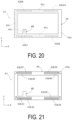
- FIG. 20 is a plan view illustrating a first electrode member of a shear force sensor according to a fourth embodiment.
- FIG. 21 is a plan view illustrating a second electrode member of the shear force sensor according to the fourth embodiment.
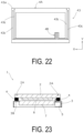
- FIG. 22 is a rear view illustrating the second electrode member of the shear force sensor according to the fourth embodiment.
- one band-like first electrode 42b is disposed on both sides excluding the central portion of the long side of the opposed surface to the elastic member 41 of the first substrate 42a. Specifically, a first electrode 42b7 is on the lower left, a first electrode 42b8 is on the lower right, a first electrode 42b9 is on the upper left, and a first electrode 42b 10 is on the upper right in plan view of the drawing.
- one set of a pair of the second electrodes 43b and 43b are disposed on both ends of the long side of the opposed surface to the elastic member 41 of the second substrate 43a.
- a set of a second electrode 43b33 and a second electrode 43b34 are on the lower left
- a set of a second electrode 43b35 and a second electrode 43b36 on the lower right
- a set of a second electrode 43b37 and a second electrode 43b38 are on the upper left
- a set of a second electrode 43b39 and a second electrode 43b40 are on the upper right in plan view of the drawing.
- first electrode member 42 As illustrated in FIG. 20 , between the first electrode 42b7 and the first electrode 42b8, between the first electrode 42b7 and the first electrode 42b9, and between the first electrode 42b9 and the first electrode 42b 10 are connected with the first lead-out wiring line 42c. Further, the first lead-out wiring line 42c is led from the first electrode 42b7 near the tongue piece portion 4B to the end portion of the tongue piece portion 4B.
- the second lead-out wiring lines 43c are connected to one ends on the short sides of the respective second electrodes 43b33 to 40 of the second substrate 43a.
- the other ends of the second lead-out wiring lines 43c, which are the side opposite to the ends connected to the second electrodes 43b33 to 40, are led in the surface not opposed to the elastic member 41 of the second substrate 43a via through holes (not illustrated) provided in portions indicated by black circles in the drawing.
- the second lead-out wiring lines 43c are shorted in the surface not opposed to the elastic member 41 of the second substrate 43a, aggregated into four, and led to the end portion of the tongue piece portion 4B.
- the second electrode 43b33 and the second electrode 43b38, the second electrode 43b34 and the second electrode 43b37, the second electrode 43b35 and the second electrode 43b40, and the second electrode 43b36 and the second electrode 43b39 are shorted.
- a force (moment) of rotating the cover panel 2 can be detected from the shearing force.
- each force with respect to the cover panel 2 (F y : shear force in the Y direction, F z : force in the Z direction, M y : moment about an axis parallel to the Y-axis passing through the center of the upper surface of the cover panel, M z : moment about an axis parallel to the Z-axis passing through the center of the upper surface of the cover panel) is expressed as in the following Formula 4 when, for example, the shape of the cover panel and the arrangement of the detection electrodes are point symmetry.
- the side wall portion 3C may be eliminated from the housing 3.
- the housing 3 provided with the side wall portion 3C is more preferred. This is because when the end surface of the cover panel 2 is exposed, the finger is injured when the finger touches the end surface of the cover panel 2, and the cover panel 2 is likely to crack when the information input device 1 falls.
- the outer diameter of the shear force sensor 4 is matched with the dimension of the housing portion 3A of the housing 3 in consideration of the deformation in the horizontal direction of the elastic member 41.
- a clearance of 0.1 mm or more where nothing is present always exists between the end surfaces at the four sides of the cover panel 2 and the side wall portion 3C of the housing 3.
- the information input device 1 of the present invention is not limited to this.
- a shock-absorbing member 9 may be provided in this clearance.
- a clearance having a sufficient dimension is formed such that the end surface of the cover panel 2 is not damaged by contact with the side wall portion 3C of the housing 3 when the elastic member 41 deforms in the horizontal direction, for example, dust accumulates in the clearance, possibly damaging the appearance. Therefore, providing the shock-absorbing member 9 in the clearance allows minimizing the dimension of the clearance.
- the shock-absorbing member 9 may be adhered to both of the end surface of the cover panel 2 and the side wall portion 3C of the housing 3 or may be adhered to either one of them.
- the clearance in which the shock-absorbing member 9 is provided is preferably 0.5 mm or less.
- a material such as various elastomers, such as a silicone elastomer and a urethane elastomer, and a gel-like body and a form thereof can be used.
- the shock-absorbing member 9 is not only in a clearance between the end surfaces at the four sides of the cover panel 2 and the side wall portion 3C of the housing 3, but also reaches the clearance between the end surface of the shear force sensor 4 and the side wall portion 3C of the housing 3.
- the shock-absorbing member 9 may be present only in the clearances between the end surfaces at the four sides of the cover panel 2 and the side wall portion 3C of the housing 3, but is more preferably also reaches the clearance between the end surface of the shear force sensor 4 and the side wall portion 3C of the housing 3. This is because the larger the area of the shock-absorbing member 9 is, the better the durability of the shock-absorbing member 9 against compression by the cover panel 2. Additionally, this allows easily disposing the shock-absorbing member 9 in the clearance.
- a soft material such as a urethane resin film, may be used for the first substrate 42a of the first electrode member 42.
- the tongue piece portion 4B of the electrode member located on the side of the housing 3 is preferably deflected, and the distal end of the tongue piece portion 4B is preferably inserted into the connector 52 provided on the substrate 51 of the detection circuit 5.
- a soft material such as a urethane resin film, may be used for the second substrate 43a of the second electrode member 43.
- At least a coefficient of friction of a region on which a shear force input is performed in the operating surface of the cover panel 2 may be larger than a coefficient of friction of the region other than that.
- a surface treatment is performed on the operating surface made of a glass sheet of the cover panel 2, such as a smartphone, with a fluorine-based coating agent to improve a slip of a finger.
- a fluorine-based coating agent to improve a slip of a finger.
- the coefficient of friction of the operating surface can be increased by sticking a sheet having a high coefficient of friction, such as a rubber, an elastomer, and a resin film, to the cover panel 2.
- fine unevenness processing such as sticking a molded article with fine unevenness surface generated by cast molding or injection molding, is performed on the cover panel 2, thus allowing the increase in coefficient of friction of the operating surface.
- the coefficient of friction can be increased by forming a projection or a depression in the cover panel 2.
- the projection can be any shape, such as a button shape or a line shape.
- FIG. 27 is a diagram illustrating an example of a region having a large coefficient of friction in the cover panel.
- a region 2C having a large coefficient of friction is provided outside a display region of the cover panel 2.
- the region 2C having a large coefficient of friction is provided inside a display region 2B of the cover panel 2.
- the sheet such as the rubber described above, may be removable except when the input by shear force is performed.
- the shear force sensor 4 has the structure layered in the order of the first electrode member 42, the elastic member 41, and the second electrode member 43 from the side of the cover panel 2.
- the layer arrangement of the first electrode member 42 and the second electrode member 43 may be switched. That is, the shear force sensor 4 may have a structure layered in the order of the second electrode member 43, the elastic member 41, and the first electrode member 42 from the side of the cover panel 2.
- the GND layer 42d is not provided on the first electrode member 42, and a GND layer 43d is provided on the second electrode member 43. More specifically, the GND layer 43d of the second electrode member 43 is disposed on the surface on the side opposite to the side of the elastic member 41 of the second substrate 43a.
- the frame-shaped shear force sensor 4 has the rectangular shape including the long sides and the short sides, but the electrode arrangement may be switched between the short sides and the long sides.
- the shape may be a square with sides having the same length.
- the shape may be a polygon other than a rectangle (a generic term of a rectangle and a square in this Description).
- the first substrate 42a and the second substrate 43a include the tongue piece portions 4B projecting inward from the inner diameters of the frame portions 4A, but may be formed of only the frame portions 4A without the tongue piece portions 4B. In this case, an FPC is mounted separately.
- the capacitive touch sensor 6 is stuck to the back surface center of the cover panel 2 to provide the touch input function to the cover panel 2, but the capacitive touch sensor 6 need not be provided.
- the cover panel 2 need not impart the touch input function itself.
- the resin described above is used for the material of the elastic member 41, but when an excessive force is applied, the elastic member 41 cannot be restored to the original shape even when the force is unloaded, which possibly results in measurement error.
- the problem of non-restoration of the shape of the elastic member 41 can be solved by performing calibration from information of presence/absence of a contact or proximity of an object to the operating surface of the cover panel 2 by the touch sensor 6 provided on the back surface of the cover panel 2.
- the information input device of the present invention excellent in durability and visibility and configured to detect the shear force has been described above, and an example of applications achievable by the information input device 1 will be described below.
- the information input device of the present invention is effectively used for electronic devices, such as a mobile phone, a smartphone, a PDA, a car navigation device, a digital camera, a digital video camera, a gaming device, and a tablet, and can be used to improve multi-function and operability of the electronic device.
- electronic devices such as a mobile phone, a smartphone, a PDA, a car navigation device, a digital camera, a digital video camera, a gaming device, and a tablet, and can be used to improve multi-function and operability of the electronic device.
Landscapes
- Engineering & Computer Science (AREA)
- Theoretical Computer Science (AREA)
- General Engineering & Computer Science (AREA)
- Physics & Mathematics (AREA)
- Human Computer Interaction (AREA)
- General Physics & Mathematics (AREA)
- Computer Hardware Design (AREA)
- Quality & Reliability (AREA)
- Computer Networks & Wireless Communication (AREA)
- Electromagnetism (AREA)
- Force Measurement Appropriate To Specific Purposes (AREA)
- Position Input By Displaying (AREA)
Claims (8)
- Informationseingabevorrichtung (1), umfassend:eine Abdeckplatte (2);ein Gehäuse (3), das einen Stützabschnitt (3B) einschließt, der eine Umfangskante (2A) der Abdeckplatte (2) von einer Rückoberfläche aus stützt;eine Scherkrafterfassungsstruktur (4), die zwischen der Umfangskante (2A) der Abdeckplatte (2) und dem Stützabschnitt (3B) des Gehäuses (3) vorgesehen ist, wobei die Scherkrafterfassungsstruktur (4) eine horizontale Eingabe in Bezug auf eine Oberfläche der Abdeckplatte (2) detektiert; undeine Detektionsschaltung (5), die mit der Scherkrafterfassungsstruktur (4) verbunden ist,wobeidie Scherkrafterfassungsstruktur (4) eine Struktur aufweist, bei der ein erstes Elektrodenelement (42), ein elastisches Element (41) und ein zweites Elektrodenelement (43) in einer Reihenfolge von einer Seite der Abdeckplatte (2) aus geschichtet sind,das erste Elektrodenelement (42) Folgendes einschließt:ein erstes Substrat (42a), das mindestens einen ersten rahmenförmigen Abschnitt (4A) aufweist;eine bandartige erste Elektrode (42b), die in einem linearen Muster auf einer dem elastischen Element (41) des ersten rahmenförmigen Abschnitts (4A) des ersten Substrats (42a) gegenüberliegenden Oberfläche vorgesehen ist; undeine erste herausführende Verdrahtungsleitung (42c), die auf dem ersten Substrat (42a) bereitgestellt und mit der ersten Elektrode (42b) verbunden ist, unddas zweite Elektrodenelement (43) Folgendes einschließt:ein zweites Substrat (43a), das mindestens einen zweiten rahmenförmigen Abschnitt (4A) aufweist;ein Paar bandartiger zweiter Elektroden (43b), die auf einer dem elastischen Element (41) des zweiten rahmenförmigen Abschnitts (4A) des zweiten Substrats (43a) gegenüberliegenden Oberfläche so vorgesehen sind, dass sie parallel zu der ersten Elektrode (42b) sind und jede des Paars der bandartigen zweiten Elektroden in einer Draufsicht teilweise mit der ersten Elektrode (42b) überlappt; undeine zweite herausführende Verdrahtungsleitung (43c), die auf dem zweiten Substrat (43a) bereitgestellt und mit der zweiten Elektrode (43b) verbunden ist, wobeijedes des ersten Substrats (42a) und des zweiten Substrats (43a) einen Laschenstückabschnitt (4B) einschließt, der von einem Innendurchmesser des jeweiligen ersten und zweiten rahmenförmigen Abschnitts (4A) nach innen vorspringt, unddie erste herausführende Verdrahtungsleitung (42c) und die zweite herausführende Verdrahtungsleitung (43c) zu Endabschnitten der Laschenstückabschnitte (4B) geführt sind, wobeiein Substrat (51) der Detektionsschaltung (5) an der Seite des Gehäuses (3) befestigt ist undder Laschenstückabschnitt (4B) des Elektrodenelements (42, 43), der sich auf einer Seite der Abdeckplatte (2) inmitten des ersten Elektrodenelements (42) und des zweiten Elektrodenelements (43) befindet, abgelenkt ist und der Laschenstückabschnitt (4B) ein distales Ende aufweist, das in einen Verbinder (52) eingeführt ist, der auf dem Substrat (51) der Detektionsschaltung (5) bereitgestellt ist.
- Informationseingabevorrichtung (1) nach Anspruch 1, wobei
die Abdeckplatte (2) eine rechteckige Form aufweist. - Informationseingabevorrichtung (1) nach Anspruch 2, wobeidie erste Elektrode (42b1, 42b2) auf einer Seite des ersten rahmenförmigen Abschnitts (4A) des ersten Substrats (42a) vorgesehen ist unddas Paar zweiter Elektroden (43b1-43b4) auf einer Seite, die der Seite gegenüberliegt, auf der die erste Elektrode (42b1, 42b2) auf der ersten Elektrode (42b1, 42b2) vorgesehen ist, des zweiten rahmenförmigen Abschnitts (4A) des zweiten Substrats (43a) vorgesehen ist.
- Informationseingabevorrichtung (1) nach Anspruch 3, wobeidas erste Elektrodenelement (42) zwei erste Elektroden (42b1-42b4) umfasst und das zweite Elektrodenelement (43) zwei Paare zweiter Elektroden (43b1-43b8) umfasst,jede der ersten Elektroden (42b1-42b4) auf einer jeweiligen von zwei parallelen Seiten des ersten rahmenförmigen Abschnitts (4A) des ersten Substrats (42a) vorgesehen ist undjede des Paars der zweiten Elektroden (43b1-43b8) auf einer jeweiligen von zwei Seiten, die den zwei Seiten gegenüberliegen, auf denen die ersten Elektroden (42b1-42b4) auf dem ersten Substrat (42a) vorgesehen sind, des zweiten rahmenförmigen Abschnitts (4A) des zweiten Substrats (43a) vorgesehen ist.
- Informationseingabevorrichtung (1) nach Anspruch 3, wobeidas erste Elektrodenelement (42) vier erste Elektroden (42b1-42b4) umfasst und das zweite Elektrodenelement (43) vier Paare zweiter Elektroden (43b1-43b8) umfasst,jede der ersten Elektroden (42b1-42b4) auf einer jeweiligen von vier Seiten des ersten rahmenförmigen Abschnitts (4A) des ersten Substrats (42a) vorgesehen ist undjede des Paars der zweiten Elektroden (43b1-43b8) auf einer jeweiligen von vier Seiten des zweiten rahmenförmigen Abschnitts (4A) des zweiten Substrats (43a) vorgesehen ist.
- Informationseingabevorrichtung (1) nach Anspruch 2, wobeidie erste Elektrode (42b5, 42b6) in einem aus einer Vielzahl von linearen Abschnitten ausgebildeten Zickzackmuster auf einer Seite auf dem ersten rahmenförmigen Abschnitt (4A) des ersten Substrats (42a) vorgesehen ist undPaare zweiter Elektroden (43b9-43b32) auf einer Seite, die der Seite gegenüberliegt, auf der die erste Elektrode (42b5, 42b6) des ersten Substrats (42a) vorgesehen ist, des zweiten rahmenförmigen Abschnitts (4A) des zweiten Substrats (43a) durch eine Anzahl der linearen Abschnitte in dem Zickzackmuster der ersten Elektrode (42b5, 42b6) vorgesehen sind.
- Informationseingabevorrichtung (1) nach einem der Ansprüche 1 bis 6, wobeidas Gehäuse (3) einen rahmenförmigen Seitenwandabschnitt (3C) einschließt, der Seitenwandabschnitt von dem Stützabschnitt (3B) so absteht, dass er eine Endoberfläche der Abdeckplatte (2) umgibt, unddie Scherkrafterfassungsstruktur (4) und eine Außenkante der Abdeckplatte (2) einen Abstand von dem Seitenwandabschnitt (3C) beibehalten.
- Informationseingabevorrichtung (1) nach Anspruch 7, umfassend
ein stoßdämpfendes Element (9), das zwischen der Endoberfläche der Abdeckplatte (2) und dem Seitenwandabschnitt (3C) des Gehäuses (3) bereitgestellt ist.
Applications Claiming Priority (2)
| Application Number | Priority Date | Filing Date | Title |
|---|---|---|---|
| JP2020029030A JP7035102B2 (ja) | 2020-02-25 | 2020-02-25 | せん断力を検出可能な情報入力装置 |
| PCT/JP2021/001589 WO2021171834A1 (ja) | 2020-02-25 | 2021-01-19 | せん断力を検出可能な情報入力装置 |
Publications (3)
| Publication Number | Publication Date |
|---|---|
| EP4064012A1 EP4064012A1 (de) | 2022-09-28 |
| EP4064012A4 EP4064012A4 (de) | 2023-01-25 |
| EP4064012B1 true EP4064012B1 (de) | 2024-06-19 |
Family
ID=77490880
Family Applications (1)
| Application Number | Title | Priority Date | Filing Date |
|---|---|---|---|
| EP21759715.2A Active EP4064012B1 (de) | 2020-02-25 | 2021-01-19 | Informationseingabevorrichtung zur detektion von scherkraft |
Country Status (7)
| Country | Link |
|---|---|
| US (1) | US11960692B2 (de) |
| EP (1) | EP4064012B1 (de) |
| JP (1) | JP7035102B2 (de) |
| KR (1) | KR20220140698A (de) |
| CN (1) | CN115210678A (de) |
| TW (1) | TWI844758B (de) |
| WO (1) | WO2021171834A1 (de) |
Families Citing this family (5)
| Publication number | Priority date | Publication date | Assignee | Title |
|---|---|---|---|---|
| US20240353966A1 (en) * | 2021-07-05 | 2024-10-24 | Nippon Telegraph And Telephone Corporation | Operating terminal, operating method, and program |
| FR3147024A1 (fr) * | 2022-05-12 | 2024-09-27 | Karim AIT CHERIF | Dispositif d’interface homme machine |
| WO2024200154A1 (fr) * | 2023-03-24 | 2024-10-03 | Ait Cherif Karim | Dispositif d'interface homme machine |
| JP2025008249A (ja) * | 2023-07-04 | 2025-01-20 | Nissha株式会社 | 入力装置 |
| WO2025069941A1 (ja) * | 2023-09-29 | 2025-04-03 | 株式会社村田製作所 | 電子機器 |
Citations (4)
| Publication number | Priority date | Publication date | Assignee | Title |
|---|---|---|---|---|
| US20140174204A1 (en) * | 2012-12-20 | 2014-06-26 | Industrial Technology Research Institute | Capacitive shear force sensor and method for fabricating thereof |
| US9336969B2 (en) * | 2007-11-29 | 2016-05-10 | Sony Corporation | Press detection sensor, input device and electronic apparatus |
| US20180356299A1 (en) * | 2016-02-29 | 2018-12-13 | Nissha Co., Ltd. | Pressure detecting device |
| US10198116B2 (en) * | 2015-04-24 | 2019-02-05 | Shenzhen New Degree Technology Co., Ltd. | Pressure sensing device, pressure measuring apparatus, touch control board, and display apparatus |
Family Cites Families (11)
| Publication number | Priority date | Publication date | Assignee | Title |
|---|---|---|---|---|
| US5241308A (en) * | 1990-02-22 | 1993-08-31 | Paragon Systems, Inc. | Force sensitive touch panel |
| CN102103443B (zh) * | 2004-04-14 | 2013-02-27 | 电子触控产品解决方案公司 | 接触式传感器、接触式传感器系统和检测接触的方法 |
| US20120098767A1 (en) * | 2009-03-31 | 2012-04-26 | Nissha Printing Co., Ltd. | Information input apparatus and pressure detection unit used in the information input apparatus |
| JP5202578B2 (ja) * | 2010-06-03 | 2013-06-05 | 日本写真印刷株式会社 | 圧力検出部及び圧力検出部を備えた情報入力装置 |
| US9229592B2 (en) * | 2013-03-14 | 2016-01-05 | Synaptics Incorporated | Shear force detection using capacitive sensors |
| JP6106011B2 (ja) * | 2013-04-05 | 2017-03-29 | 日本写真印刷株式会社 | 圧力検出装置 |
| US20170045976A1 (en) * | 2015-08-10 | 2017-02-16 | Apple Inc. | Electronic Devices With Shear Force Sensing |
| US9886057B2 (en) * | 2015-09-22 | 2018-02-06 | Apple Inc. | Electronic device with enhanced pressure resistant features |
| US10019085B2 (en) * | 2015-09-30 | 2018-07-10 | Apple Inc. | Sensor layer having a patterned compliant layer |
| US20180081400A1 (en) * | 2016-09-21 | 2018-03-22 | Apple Inc. | Electronic devices with sealing elements having embedded sensors |
| TWI671509B (zh) * | 2018-01-05 | 2019-09-11 | 財團法人工業技術研究院 | 觸覺感測器 |
-
2020
- 2020-02-25 JP JP2020029030A patent/JP7035102B2/ja active Active
-
2021
- 2021-01-19 EP EP21759715.2A patent/EP4064012B1/de active Active
- 2021-01-19 KR KR1020227021433A patent/KR20220140698A/ko not_active Abandoned
- 2021-01-19 US US17/904,563 patent/US11960692B2/en active Active
- 2021-01-19 WO PCT/JP2021/001589 patent/WO2021171834A1/ja not_active Ceased
- 2021-01-19 CN CN202180016464.XA patent/CN115210678A/zh not_active Withdrawn
- 2021-01-25 TW TW110102636A patent/TWI844758B/zh active
Patent Citations (4)
| Publication number | Priority date | Publication date | Assignee | Title |
|---|---|---|---|---|
| US9336969B2 (en) * | 2007-11-29 | 2016-05-10 | Sony Corporation | Press detection sensor, input device and electronic apparatus |
| US20140174204A1 (en) * | 2012-12-20 | 2014-06-26 | Industrial Technology Research Institute | Capacitive shear force sensor and method for fabricating thereof |
| US10198116B2 (en) * | 2015-04-24 | 2019-02-05 | Shenzhen New Degree Technology Co., Ltd. | Pressure sensing device, pressure measuring apparatus, touch control board, and display apparatus |
| US20180356299A1 (en) * | 2016-02-29 | 2018-12-13 | Nissha Co., Ltd. | Pressure detecting device |
Also Published As
| Publication number | Publication date |
|---|---|
| EP4064012A4 (de) | 2023-01-25 |
| TW202202991A (zh) | 2022-01-16 |
| US20230089017A1 (en) | 2023-03-23 |
| TWI844758B (zh) | 2024-06-11 |
| KR20220140698A (ko) | 2022-10-18 |
| JP2021135555A (ja) | 2021-09-13 |
| CN115210678A (zh) | 2022-10-18 |
| US11960692B2 (en) | 2024-04-16 |
| JP7035102B2 (ja) | 2022-03-14 |
| EP4064012A1 (de) | 2022-09-28 |
| WO2021171834A1 (ja) | 2021-09-02 |
Similar Documents
| Publication | Publication Date | Title |
|---|---|---|
| EP4064012B1 (de) | Informationseingabevorrichtung zur detektion von scherkraft | |
| US9158383B2 (en) | Force concentrator | |
| JP5821322B2 (ja) | 検出装置、電子機器及びロボット | |
| JP4545168B2 (ja) | 力イメージング入力のデバイスとシステム | |
| JP5347913B2 (ja) | センサ装置、電子機器、及びセンサ装置の製造方法 | |
| CN102539025A (zh) | 检测装置、电子仪器以及机器人 | |
| WO2009157614A1 (en) | Touch inputting apparatus integral sensors and method for acquiring location and intensity of force | |
| US20160378249A1 (en) | Input device, display apparatus and terminal apparatus | |
| KR101920014B1 (ko) | 압력 센서 및 이를 구비하는 터치 입력 장치 | |
| JP2013152129A (ja) | 力検出器、圧力検出装置、電子機器及びロボット | |
| JP2013117458A (ja) | 検出装置、電子機器及びロボット | |
| JP2013108754A (ja) | 力検出器、検出装置、電子機器及びロボット | |
| JP2012108021A (ja) | 検出装置、電子機器及びロボット | |
| JP2012098148A (ja) | 圧力検出装置、電子機器、及びロボット | |
| JP2013113760A (ja) | 検出装置、電子機器及びロボット | |
| JP2012026907A (ja) | 検出装置、電子機器及びロボット | |
| KR101645159B1 (ko) | 사인패드 장치 | |
| US10051724B1 (en) | Structural ground reference for an electronic component of a computing device | |
| JP2005352632A (ja) | 入力装置およびこの入力装置を用いた表示入力装置 | |
| JP2012088264A (ja) | 圧力検出装置、電子機器 |
Legal Events
| Date | Code | Title | Description |
|---|---|---|---|
| STAA | Information on the status of an ep patent application or granted ep patent |
Free format text: STATUS: THE INTERNATIONAL PUBLICATION HAS BEEN MADE |
|
| PUAI | Public reference made under article 153(3) epc to a published international application that has entered the european phase |
Free format text: ORIGINAL CODE: 0009012 |
|
| STAA | Information on the status of an ep patent application or granted ep patent |
Free format text: STATUS: REQUEST FOR EXAMINATION WAS MADE |
|
| 17P | Request for examination filed |
Effective date: 20220621 |
|
| AK | Designated contracting states |
Kind code of ref document: A1 Designated state(s): AL AT BE BG CH CY CZ DE DK EE ES FI FR GB GR HR HU IE IS IT LI LT LU LV MC MK MT NL NO PL PT RO RS SE SI SK SM TR |
|
| A4 | Supplementary search report drawn up and despatched |
Effective date: 20221223 |
|
| RIC1 | Information provided on ipc code assigned before grant |
Ipc: G06F 1/16 20060101ALI20221219BHEP Ipc: G06F 3/041 20060101AFI20221219BHEP |
|
| STAA | Information on the status of an ep patent application or granted ep patent |
Free format text: STATUS: EXAMINATION IS IN PROGRESS |
|
| 17Q | First examination report despatched |
Effective date: 20230426 |
|
| DAV | Request for validation of the european patent (deleted) | ||
| DAX | Request for extension of the european patent (deleted) | ||
| GRAP | Despatch of communication of intention to grant a patent |
Free format text: ORIGINAL CODE: EPIDOSNIGR1 |
|
| STAA | Information on the status of an ep patent application or granted ep patent |
Free format text: STATUS: GRANT OF PATENT IS INTENDED |
|
| RIC1 | Information provided on ipc code assigned before grant |
Ipc: G06F 1/16 20060101ALI20240116BHEP Ipc: G06F 3/0354 20130101ALI20240116BHEP Ipc: G06F 3/041 20060101AFI20240116BHEP |
|
| INTG | Intention to grant announced |
Effective date: 20240201 |
|
| GRAJ | Information related to disapproval of communication of intention to grant by the applicant or resumption of examination proceedings by the epo deleted |
Free format text: ORIGINAL CODE: EPIDOSDIGR1 |
|
| STAA | Information on the status of an ep patent application or granted ep patent |
Free format text: STATUS: EXAMINATION IS IN PROGRESS |
|
| INTC | Intention to grant announced (deleted) | ||
| GRAP | Despatch of communication of intention to grant a patent |
Free format text: ORIGINAL CODE: EPIDOSNIGR1 |
|
| STAA | Information on the status of an ep patent application or granted ep patent |
Free format text: STATUS: GRANT OF PATENT IS INTENDED |
|
| GRAS | Grant fee paid |
Free format text: ORIGINAL CODE: EPIDOSNIGR3 |
|
| INTG | Intention to grant announced |
Effective date: 20240417 |
|
| GRAA | (expected) grant |
Free format text: ORIGINAL CODE: 0009210 |
|
| STAA | Information on the status of an ep patent application or granted ep patent |
Free format text: STATUS: THE PATENT HAS BEEN GRANTED |
|
| AK | Designated contracting states |
Kind code of ref document: B1 Designated state(s): AL AT BE BG CH CY CZ DE DK EE ES FI FR GB GR HR HU IE IS IT LI LT LU LV MC MK MT NL NO PL PT RO RS SE SI SK SM TR |
|
| REG | Reference to a national code |
Ref country code: GB Ref legal event code: FG4D |
|
| REG | Reference to a national code |
Ref country code: CH Ref legal event code: EP |
|
| REG | Reference to a national code |
Ref country code: DE Ref legal event code: R096 Ref document number: 602021014627 Country of ref document: DE |
|
| PG25 | Lapsed in a contracting state [announced via postgrant information from national office to epo] |
Ref country code: BG Free format text: LAPSE BECAUSE OF FAILURE TO SUBMIT A TRANSLATION OF THE DESCRIPTION OR TO PAY THE FEE WITHIN THE PRESCRIBED TIME-LIMIT Effective date: 20240619 |
|
| PG25 | Lapsed in a contracting state [announced via postgrant information from national office to epo] |
Ref country code: FI Free format text: LAPSE BECAUSE OF FAILURE TO SUBMIT A TRANSLATION OF THE DESCRIPTION OR TO PAY THE FEE WITHIN THE PRESCRIBED TIME-LIMIT Effective date: 20240619 Ref country code: HR Free format text: LAPSE BECAUSE OF FAILURE TO SUBMIT A TRANSLATION OF THE DESCRIPTION OR TO PAY THE FEE WITHIN THE PRESCRIBED TIME-LIMIT Effective date: 20240619 |
|
| REG | Reference to a national code |
Ref country code: LT Ref legal event code: MG9D |
|
| PG25 | Lapsed in a contracting state [announced via postgrant information from national office to epo] |
Ref country code: GR Free format text: LAPSE BECAUSE OF FAILURE TO SUBMIT A TRANSLATION OF THE DESCRIPTION OR TO PAY THE FEE WITHIN THE PRESCRIBED TIME-LIMIT Effective date: 20240920 |
|
| REG | Reference to a national code |
Ref country code: NL Ref legal event code: MP Effective date: 20240619 |
|
| PG25 | Lapsed in a contracting state [announced via postgrant information from national office to epo] |
Ref country code: LV Free format text: LAPSE BECAUSE OF FAILURE TO SUBMIT A TRANSLATION OF THE DESCRIPTION OR TO PAY THE FEE WITHIN THE PRESCRIBED TIME-LIMIT Effective date: 20240619 |
|
| PG25 | Lapsed in a contracting state [announced via postgrant information from national office to epo] |
Ref country code: NO Free format text: LAPSE BECAUSE OF FAILURE TO SUBMIT A TRANSLATION OF THE DESCRIPTION OR TO PAY THE FEE WITHIN THE PRESCRIBED TIME-LIMIT Effective date: 20240919 Ref country code: LV Free format text: LAPSE BECAUSE OF FAILURE TO SUBMIT A TRANSLATION OF THE DESCRIPTION OR TO PAY THE FEE WITHIN THE PRESCRIBED TIME-LIMIT Effective date: 20240619 Ref country code: HR Free format text: LAPSE BECAUSE OF FAILURE TO SUBMIT A TRANSLATION OF THE DESCRIPTION OR TO PAY THE FEE WITHIN THE PRESCRIBED TIME-LIMIT Effective date: 20240619 Ref country code: GR Free format text: LAPSE BECAUSE OF FAILURE TO SUBMIT A TRANSLATION OF THE DESCRIPTION OR TO PAY THE FEE WITHIN THE PRESCRIBED TIME-LIMIT Effective date: 20240920 Ref country code: FI Free format text: LAPSE BECAUSE OF FAILURE TO SUBMIT A TRANSLATION OF THE DESCRIPTION OR TO PAY THE FEE WITHIN THE PRESCRIBED TIME-LIMIT Effective date: 20240619 Ref country code: BG Free format text: LAPSE BECAUSE OF FAILURE TO SUBMIT A TRANSLATION OF THE DESCRIPTION OR TO PAY THE FEE WITHIN THE PRESCRIBED TIME-LIMIT Effective date: 20240619 Ref country code: RS Free format text: LAPSE BECAUSE OF FAILURE TO SUBMIT A TRANSLATION OF THE DESCRIPTION OR TO PAY THE FEE WITHIN THE PRESCRIBED TIME-LIMIT Effective date: 20240919 |
|
| PG25 | Lapsed in a contracting state [announced via postgrant information from national office to epo] |
Ref country code: NL Free format text: LAPSE BECAUSE OF FAILURE TO SUBMIT A TRANSLATION OF THE DESCRIPTION OR TO PAY THE FEE WITHIN THE PRESCRIBED TIME-LIMIT Effective date: 20240619 |
|
| REG | Reference to a national code |
Ref country code: AT Ref legal event code: MK05 Ref document number: 1696327 Country of ref document: AT Kind code of ref document: T Effective date: 20240619 |
|
| PG25 | Lapsed in a contracting state [announced via postgrant information from national office to epo] |
Ref country code: NL Free format text: LAPSE BECAUSE OF FAILURE TO SUBMIT A TRANSLATION OF THE DESCRIPTION OR TO PAY THE FEE WITHIN THE PRESCRIBED TIME-LIMIT Effective date: 20240619 |
|
| PG25 | Lapsed in a contracting state [announced via postgrant information from national office to epo] |
Ref country code: PT Free format text: LAPSE BECAUSE OF FAILURE TO SUBMIT A TRANSLATION OF THE DESCRIPTION OR TO PAY THE FEE WITHIN THE PRESCRIBED TIME-LIMIT Effective date: 20241021 |
|
| PG25 | Lapsed in a contracting state [announced via postgrant information from national office to epo] |
Ref country code: PT Free format text: LAPSE BECAUSE OF FAILURE TO SUBMIT A TRANSLATION OF THE DESCRIPTION OR TO PAY THE FEE WITHIN THE PRESCRIBED TIME-LIMIT Effective date: 20241021 |
|
| PG25 | Lapsed in a contracting state [announced via postgrant information from national office to epo] |
Ref country code: PL Free format text: LAPSE BECAUSE OF FAILURE TO SUBMIT A TRANSLATION OF THE DESCRIPTION OR TO PAY THE FEE WITHIN THE PRESCRIBED TIME-LIMIT Effective date: 20240619 |
|
| PG25 | Lapsed in a contracting state [announced via postgrant information from national office to epo] |
Ref country code: EE Free format text: LAPSE BECAUSE OF FAILURE TO SUBMIT A TRANSLATION OF THE DESCRIPTION OR TO PAY THE FEE WITHIN THE PRESCRIBED TIME-LIMIT Effective date: 20240619 |
|
| PG25 | Lapsed in a contracting state [announced via postgrant information from national office to epo] |
Ref country code: IS Free format text: LAPSE BECAUSE OF FAILURE TO SUBMIT A TRANSLATION OF THE DESCRIPTION OR TO PAY THE FEE WITHIN THE PRESCRIBED TIME-LIMIT Effective date: 20241019 Ref country code: AT Free format text: LAPSE BECAUSE OF FAILURE TO SUBMIT A TRANSLATION OF THE DESCRIPTION OR TO PAY THE FEE WITHIN THE PRESCRIBED TIME-LIMIT Effective date: 20240619 |
|
| PG25 | Lapsed in a contracting state [announced via postgrant information from national office to epo] |
Ref country code: CZ Free format text: LAPSE BECAUSE OF FAILURE TO SUBMIT A TRANSLATION OF THE DESCRIPTION OR TO PAY THE FEE WITHIN THE PRESCRIBED TIME-LIMIT Effective date: 20240619 |
|
| PG25 | Lapsed in a contracting state [announced via postgrant information from national office to epo] |
Ref country code: SK Free format text: LAPSE BECAUSE OF FAILURE TO SUBMIT A TRANSLATION OF THE DESCRIPTION OR TO PAY THE FEE WITHIN THE PRESCRIBED TIME-LIMIT Effective date: 20240619 Ref country code: RO Free format text: LAPSE BECAUSE OF FAILURE TO SUBMIT A TRANSLATION OF THE DESCRIPTION OR TO PAY THE FEE WITHIN THE PRESCRIBED TIME-LIMIT Effective date: 20240619 |
|
| PG25 | Lapsed in a contracting state [announced via postgrant information from national office to epo] |
Ref country code: ES Free format text: LAPSE BECAUSE OF FAILURE TO SUBMIT A TRANSLATION OF THE DESCRIPTION OR TO PAY THE FEE WITHIN THE PRESCRIBED TIME-LIMIT Effective date: 20240619 Ref country code: SM Free format text: LAPSE BECAUSE OF FAILURE TO SUBMIT A TRANSLATION OF THE DESCRIPTION OR TO PAY THE FEE WITHIN THE PRESCRIBED TIME-LIMIT Effective date: 20240619 |
|
| PG25 | Lapsed in a contracting state [announced via postgrant information from national office to epo] |
Ref country code: SM Free format text: LAPSE BECAUSE OF FAILURE TO SUBMIT A TRANSLATION OF THE DESCRIPTION OR TO PAY THE FEE WITHIN THE PRESCRIBED TIME-LIMIT Effective date: 20240619 Ref country code: SK Free format text: LAPSE BECAUSE OF FAILURE TO SUBMIT A TRANSLATION OF THE DESCRIPTION OR TO PAY THE FEE WITHIN THE PRESCRIBED TIME-LIMIT Effective date: 20240619 Ref country code: RO Free format text: LAPSE BECAUSE OF FAILURE TO SUBMIT A TRANSLATION OF THE DESCRIPTION OR TO PAY THE FEE WITHIN THE PRESCRIBED TIME-LIMIT Effective date: 20240619 Ref country code: PL Free format text: LAPSE BECAUSE OF FAILURE TO SUBMIT A TRANSLATION OF THE DESCRIPTION OR TO PAY THE FEE WITHIN THE PRESCRIBED TIME-LIMIT Effective date: 20240619 Ref country code: IS Free format text: LAPSE BECAUSE OF FAILURE TO SUBMIT A TRANSLATION OF THE DESCRIPTION OR TO PAY THE FEE WITHIN THE PRESCRIBED TIME-LIMIT Effective date: 20241019 Ref country code: ES Free format text: LAPSE BECAUSE OF FAILURE TO SUBMIT A TRANSLATION OF THE DESCRIPTION OR TO PAY THE FEE WITHIN THE PRESCRIBED TIME-LIMIT Effective date: 20240619 Ref country code: EE Free format text: LAPSE BECAUSE OF FAILURE TO SUBMIT A TRANSLATION OF THE DESCRIPTION OR TO PAY THE FEE WITHIN THE PRESCRIBED TIME-LIMIT Effective date: 20240619 Ref country code: CZ Free format text: LAPSE BECAUSE OF FAILURE TO SUBMIT A TRANSLATION OF THE DESCRIPTION OR TO PAY THE FEE WITHIN THE PRESCRIBED TIME-LIMIT Effective date: 20240619 Ref country code: AT Free format text: LAPSE BECAUSE OF FAILURE TO SUBMIT A TRANSLATION OF THE DESCRIPTION OR TO PAY THE FEE WITHIN THE PRESCRIBED TIME-LIMIT Effective date: 20240619 |
|
| PG25 | Lapsed in a contracting state [announced via postgrant information from national office to epo] |
Ref country code: IT Free format text: LAPSE BECAUSE OF FAILURE TO SUBMIT A TRANSLATION OF THE DESCRIPTION OR TO PAY THE FEE WITHIN THE PRESCRIBED TIME-LIMIT Effective date: 20240619 |
|
| REG | Reference to a national code |
Ref country code: DE Ref legal event code: R097 Ref document number: 602021014627 Country of ref document: DE |
|
| PGFP | Annual fee paid to national office [announced via postgrant information from national office to epo] |
Ref country code: DE Payment date: 20250121 Year of fee payment: 5 |
|
| PG25 | Lapsed in a contracting state [announced via postgrant information from national office to epo] |
Ref country code: DK Free format text: LAPSE BECAUSE OF FAILURE TO SUBMIT A TRANSLATION OF THE DESCRIPTION OR TO PAY THE FEE WITHIN THE PRESCRIBED TIME-LIMIT Effective date: 20240619 |
|
| PGFP | Annual fee paid to national office [announced via postgrant information from national office to epo] |
Ref country code: FR Payment date: 20250128 Year of fee payment: 5 |
|
| PLBE | No opposition filed within time limit |
Free format text: ORIGINAL CODE: 0009261 |
|
| STAA | Information on the status of an ep patent application or granted ep patent |
Free format text: STATUS: NO OPPOSITION FILED WITHIN TIME LIMIT |
|
| 26N | No opposition filed |
Effective date: 20250320 |
|
| REG | Reference to a national code |
Ref country code: CH Ref legal event code: PL |
|
| PG25 | Lapsed in a contracting state [announced via postgrant information from national office to epo] |
Ref country code: SE Free format text: LAPSE BECAUSE OF FAILURE TO SUBMIT A TRANSLATION OF THE DESCRIPTION OR TO PAY THE FEE WITHIN THE PRESCRIBED TIME-LIMIT Effective date: 20240619 |
|
| PG25 | Lapsed in a contracting state [announced via postgrant information from national office to epo] |
Ref country code: MC Free format text: LAPSE BECAUSE OF FAILURE TO SUBMIT A TRANSLATION OF THE DESCRIPTION OR TO PAY THE FEE WITHIN THE PRESCRIBED TIME-LIMIT Effective date: 20240619 Ref country code: LU Free format text: LAPSE BECAUSE OF NON-PAYMENT OF DUE FEES Effective date: 20250119 |
|
| GBPC | Gb: european patent ceased through non-payment of renewal fee |
Effective date: 20250119 |
|
| PG25 | Lapsed in a contracting state [announced via postgrant information from national office to epo] |
Ref country code: BE Free format text: LAPSE BECAUSE OF NON-PAYMENT OF DUE FEES Effective date: 20250131 Ref country code: GB Free format text: LAPSE BECAUSE OF NON-PAYMENT OF DUE FEES Effective date: 20250119 |
|
| PG25 | Lapsed in a contracting state [announced via postgrant information from national office to epo] |
Ref country code: CH Free format text: LAPSE BECAUSE OF NON-PAYMENT OF DUE FEES Effective date: 20250131 |
|
| REG | Reference to a national code |
Ref country code: BE Ref legal event code: MM Effective date: 20250131 |
|
| PG25 | Lapsed in a contracting state [announced via postgrant information from national office to epo] |
Ref country code: IE Free format text: LAPSE BECAUSE OF NON-PAYMENT OF DUE FEES Effective date: 20250119 |